ultra reliable embedded computing - versalogic offer a high number ... white paper. ultra reliable...
TRANSCRIPT
A VersaLogic Focus on Reliability White Paper: Ultra Reliable Embedded Computing | p1 VERSALOGICC O R P O R A T I O N
IntroductionAdvancements in technology inevitably overtake the standards intended to ensure consistency and compliance in the implementation of technology. This tension is healthy; the rapid pace of progress forces a reassessment and modernization of industry standards. Indeed, the tension fosters innovation since, by definition, advance-ments can only be made when limits are surpassed.
Case in Point: IPC Class 3 Assembly RequirementsCompanies that purchase Commercial Off-The-Shelf (COTS) embedded computer systems often need them to be extremely reliable. For mission critical applications, companies often specify products designed and manufactured to IPC Class 3 require-ments. The IPC Class 3 standard was developed in the 1960’s to ensure the reliability of electronic products in the most demanding environments. However, with the advent of high-density printed circuit boards, new design and manufacturing challenges arise in meeting IPC Class 3 requirements. The result is that following the current IPC Class 3 guidelines is no longer always consistent with providing the most reliable product. It’s a classic case of an important standard that hasn’t kept pace with advancements in technology.
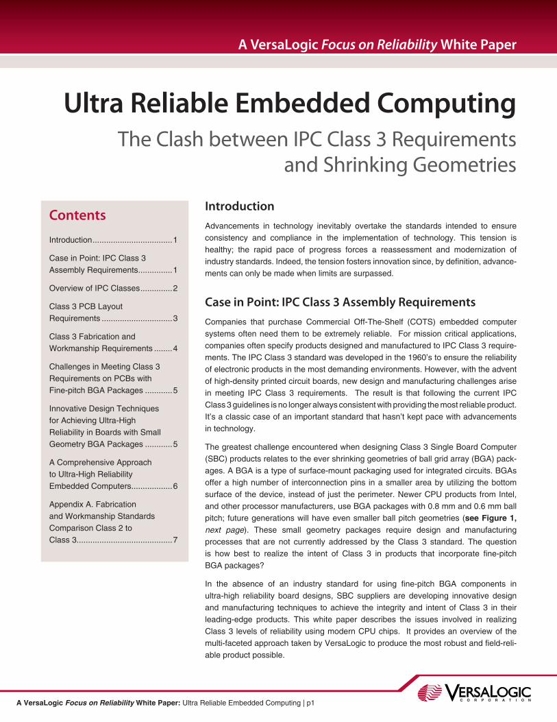
The greatest challenge encountered when designing Class 3 Single Board Computer (SBC) products relates to the ever shrinking geometries of ball grid array (BGA) pack-ages. A BGA is a type of surface-mount packaging used for integrated circuits. BGAs offer a high number of interconnection pins in a smaller area by utilizing the bottom surface of the device, instead of just the perimeter. Newer CPU products from Intel, and other processor manufacturers, use BGA packages with 0.8 mm and 0.6 mm ball pitch; future generations will have even smaller ball pitch geometries (see Figure 1, next page). These small geometry packages require design and manufacturing processes that are not currently addressed by the Class 3 standard. The question is how best to realize the intent of Class 3 in products that incorporate fine-pitch BGA packages?
In the absence of an industry standard for using fine-pitch BGA components in ultra-high reliability board designs, SBC suppliers are developing innovative design and manufacturing techniques to achieve the integrity and intent of Class 3 in their leading-edge products. This white paper describes the issues involved in realizing Class 3 levels of reliability using modern CPU chips. It provides an overview of the multi-faceted approach taken by VersaLogic to produce the most robust and field-reli-able product possible.
Contents
Introduction ...................................1
Case in Point: IPC Class 3 Assembly Requirements ...............1
Overview of IPC Classes ..............2
Class 3 PCB Layout Requirements ...............................3
Class 3 Fabrication and Workmanship Requirements ........4
Challenges in Meeting Class 3 Requirements on PCBs with Fine-pitch BGA Packages ............5
Innovative Design Techniques for Achieving Ultra-High Reliability in Boards with Small Geometry BGA Packages ............5
A Comprehensive Approach to Ultra-High Reliability Embedded Computers ..................6
Appendix A. Fabrication and Workmanship Standards Comparison Class 2 to Class 3 ..........................................7
A VersaLogic Focus on Reliability White Paper
Ultra Reliable Embedded ComputingThe Clash between IPC Class 3 Requirements
and Shrinking Geometries
A VersaLogic Focus on Reliability White Paper: Ultra Reliable Embedded Computing | p2 VERSALOGICC O R P O R A T I O N
Overview of IPC ClassesFounded in 1957, IPC, the Association Connecting Electronics Industries (originally known as the Institute for Printed Circuits, or IPC), is a trade association whose aim is to standardize the assembly and production requirements of electronic equipment and assemblies. From design and purchasing to assembly and acceptance, there is an IPC standard associated with nearly every step of production and assembly of printed circuit board assemblies.
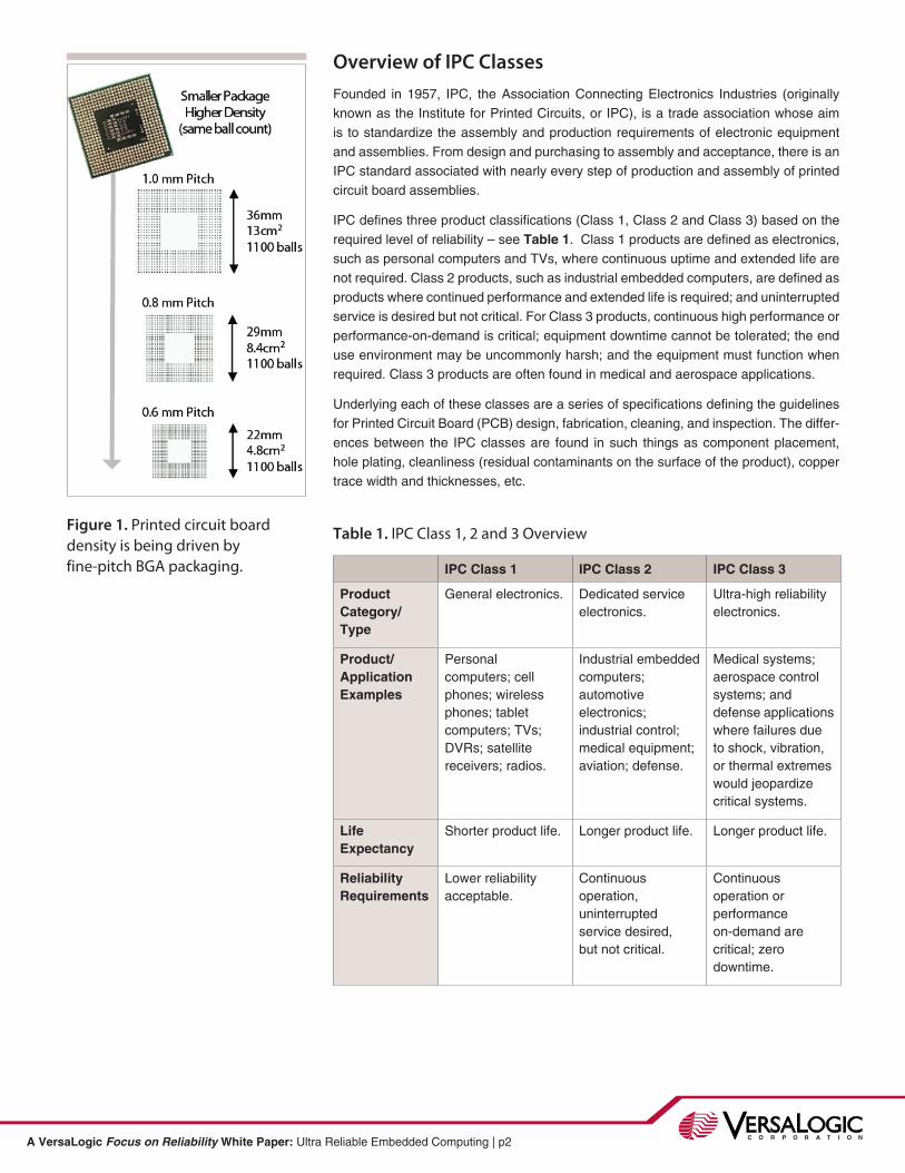
IPC defines three product classifications (Class 1, Class 2 and Class 3) based on the required level of reliability – see Table 1. Class 1 products are defined as electronics, such as personal computers and TVs, where continuous uptime and extended life are not required. Class 2 products, such as industrial embedded computers, are defined as products where continued performance and extended life is required; and uninterrupted service is desired but not critical. For Class 3 products, continuous high performance or performance-on-demand is critical; equipment downtime cannot be tolerated; the end use environment may be uncommonly harsh; and the equipment must function when required. Class 3 products are often found in medical and aerospace applications.
Underlying each of these classes are a series of specifications defining the guidelines for Printed Circuit Board (PCB) design, fabrication, cleaning, and inspection. The differ-ences between the IPC classes are found in such things as component placement, hole plating, cleanliness (residual contaminants on the surface of the product), copper trace width and thicknesses, etc.
Table 1. IPC Class 1, 2 and 3 Overview
IPC Class 1 IPC Class 2 IPC Class 3
Product Category/Type
General electronics. Dedicated service electronics.
Ultra-high reliability electronics.
Product/Application Examples
Personal computers; cell phones; wireless phones; tablet computers; TVs; DVRs; satellite receivers; radios.
Industrial embedded computers; automotive electronics; industrial control; medical equipment; aviation; defense.
Medical systems; aerospace control systems; and defense applications where failures due to shock, vibration, or thermal extremes would jeopardize critical systems.
Life Expectancy
Shorter product life. Longer product life. Longer product life.
Reliability Requirements
Lower reliability acceptable.
Continuous operation, uninterrupted service desired, but not critical.
Continuous operation or performance on-demand are critical; zero downtime.
Figure 1. Printed circuit board density is being driven by fine-pitch BGA packaging.
A VersaLogic Focus on Reliability White Paper: Ultra Reliable Embedded Computing | p3 VERSALOGICC O R P O R A T I O N
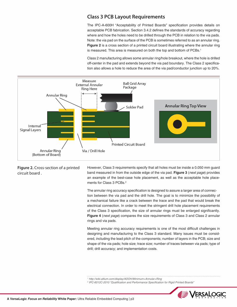
Class 3 PCB Layout RequirementsThe IPC-A-600H “Acceptability of Printed Boards” specification provides details on acceptable PCB fabrication. Section 3.4.2 defines the standards of accuracy regarding where and how the holes need to be drilled through the PCB in relation to the via pads. Note: the via pad on the surface of the PCB is sometimes referred to as an annular ring. Figure 2 is a cross section of a printed circuit board illustrating where the annular ring is measured. This area is measured on both the top and bottom of PCBs.1
Class 2 manufacturing allows some annular ring/hole breakout, where the hole is drilled off-center in the pad and extends beyond the via pad boundary. The Class 2 specifica-tion also allows a hole to reduce the area of the via pad/conductor junction up to 20%.
1 http://wiki.altium.com/display/ADOH/Minimum+Annular+Ring2 IPC-6012C-2010 “Qualification and Performance Specification for Rigid Printed Boards”
Figure 2. Cross-section of a printed circuit board .
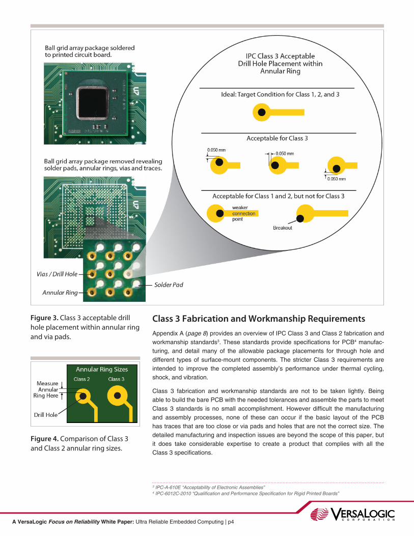
However, Class 3 requirements specify that all holes must be inside a 0.050 mm guard band measured in from the outside edge of the via pad. Figure 3 (next page) provides an example of the best-case hole placement, as well as the acceptable hole place-ments for Class 3 PCBs.2
The annular ring accuracy specification is designed to assure a larger area of connec-tion between the via pad and the drill hole. The goal is to minimize the possibility of a mechanical failure like a crack between the trace and the pad that would break the electrical connection. In order to meet the stringent drill hole placement requirements of the Class 3 specification, the size of annular rings must be enlarged significantly. Figure 4 (next page) compares the size requirements of Class 3 and Class 2 annular rings and via pads.
Meeting annular ring accuracy requirements is one of the most difficult challenges in designing and manufacturing to the Class 3 standard. Many issues must be consid-ered, including the lead pitch of the components; number of layers in the PCB; size and shape of the via pads; hole size; trace size; number of traces between via pads; type of drill; drill accuracy; and implementation costs.
A VersaLogic Focus on Reliability White Paper: Ultra Reliable Embedded Computing | p4 VERSALOGICC O R P O R A T I O N
Figure 3. Class 3 acceptable drill hole placement within annular ring and via pads.
Class 3 Fabrication and Workmanship RequirementsAppendix A (page 8) provides an overview of IPC Class 3 and Class 2 fabrication and workmanship standards3. These standards provide specifications for PCB4 manufac-turing, and detail many of the allowable package placements for through hole and different types of surface-mount components. The stricter Class 3 requirements are intended to improve the completed assembly’s performance under thermal cycling, shock, and vibration.
Class 3 fabrication and workmanship standards are not to be taken lightly. Being able to build the bare PCB with the needed tolerances and assemble the parts to meet Class 3 standards is no small accomplishment. However difficult the manufacturing and assembly processes, none of these can occur if the basic layout of the PCB has traces that are too close or via pads and holes that are not the correct size. The detailed manufacturing and inspection issues are beyond the scope of this paper, but it does take considerable expertise to create a product that complies with all the Class 3 specifications.
3 IPC-A-610E “Acceptability of Electronic Assemblies”4 IPC-6012C-2010 “Qualification and Performance Specification for Rigid Printed Boards”
Figure 4. Comparison of Class 3 and Class 2 annular ring sizes.
A VersaLogic Focus on Reliability White Paper: Ultra Reliable Embedded Computing | p5 VERSALOGICC O R P O R A T I O N
Challenges in Meeting Class 3 Requirements on PCBs with Fine-pitch BGA PackagesThe most formidable challenges encountered when designing Class 3 Single Board Computer (SBC) products have to do with the small geometries of BGA packages. As discussed earlier, newer CPU products from Intel and others, have BGA packages with ≤0.8 mm ball pitch. Unfortunately, IPC Class 3 requirements have not kept up with the rapid rate of technological change in integrated circuit packaging.
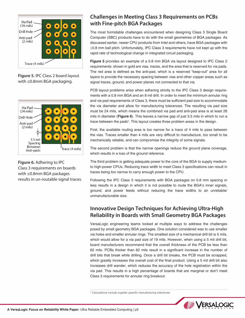
Figure 5 provides an example of a 0.8 mm BGA via layout designed to IPC Class 2 requirements: shown in gold are vias, traces, and the area that is reserved for via pads. The red area is defined as the anti-pad, which is a reserved “keep-out” area for all layers to provide the necessary spacing between vias and other copper areas such as signal traces, ground, and power planes not connected to that via.
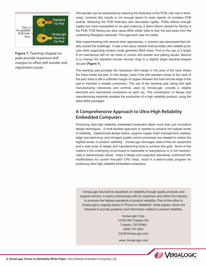
PCB layout problems arise when adhering strictly to the IPC Class 3 design require-ments with a 0.8 mm BGA and an 8 mil drill. In order to meet the minimum annular ring and via pad requirements of Class 3, there must be sufficient pad size to accommodate the via diameter and allow for manufacturing tolerances. The resulting via pad size must be 24 mils, which means the combined via pad and anti-pad area is at least 26 mils in diameter (Figure 6). This leaves a narrow gap of just 3.5 mils in which to run a trace between the pads5. This layout creates three problem areas in the design.
First, the available routing area is too narrow for a trace of 4 mils to pass between the vias. Traces smaller than 4 mils are very difficult to manufacture, too small to be mechanically reliable, and can compromise the integrity of some signals.
The second problem is that the narrow openings reduce the ground plane coverage, which results in a loss of the ground reference.
The third problem is getting adequate power to the core of the BGA to supply medium- to high-power CPUs. Reducing trace width to meet Class 3 specifications can result in traces being too narrow to carry enough power to the CPU.
Following the IPC Class 3 requirements with BGA packages on 0.8 mm spacing or less results in a design in which it is not possible to route the BGA’s inner signals, ground, and power feeds without reducing the trace widths to an unreliable/ unmanufacturable size.
Innovative Design Techniques for Achieving Ultra-High Reliability in Boards with Small Geometry BGA PackagesVersaLogic engineering teams looked at multiple ways to address the challenges posed by small geometry BGA packages. One solution considered was to use smaller via holes and smaller annular rings. The smallest size of a mechanical drill bit is 5 mils, which would allow for a via pad size of 19 mils. However, when using a 5 mil drill bit, board manufacturers recommend that the overall thickness of the PCB be less than 62 mils. PCBs thicker than 62 mils result in a significant increase in the number of drill bits that break while drilling. Once a drill bit breaks, the PCB must be scrapped, which greatly increases the overall cost of the final product. Using a 5 mil drill bit also increases drill wander, which reduces the accuracy of the hole registration within the via pad. This results in a high percentage of boards that are marginal or don’t meet Class 3 requirements for annular ring breakout.
5 Calculations include supplier specific manufacturing tolerances
Figure 5. IPC Class 2 board layout with ≤0.8mm BGA packaging.
Figure 6. Adhering to IPC Class 3 requirements on boards with ≤0.8mm BGA packages results in un-routable signal traces.
A VersaLogic Focus on Reliability White Paper: Ultra Reliable Embedded Computing | p6 VERSALOGICC O R P O R A T I O N
Figure 7. Teardrop-shaped via pads provide maximum drill margins to offset drill wander and registration issues.
VersaLogic has built its reputation on reliability through quality products and superior service. It works continuously with its customers and within the industry
to promote the highest standards of product reliability. Part of this effort is VersaLogic’s ongoing series of “Focus on Reliability” white papers, which are
intended to provide guidance and information related to product reliability.
VersaLogic Corp. 12100 SW Tualatin Rd.
Tualatin, OR 97062 (503) 747-2261
www.VersaLogic.com
Drill wander can be addressed by reducing the thickness of the PCB (<62 mils in thick-ness), however this results in not enough layers to route signals on complex PCB boards. Reducing the PCB thickness also decreases rigidity. PCBs without enough rigidity are more susceptible to via pad cratering, a latent failure caused by flexing of the PCB. PCB flexing can also cause BGA solder balls to tear the pad away from the underlying fiberglass substrate. This approach was not viable.
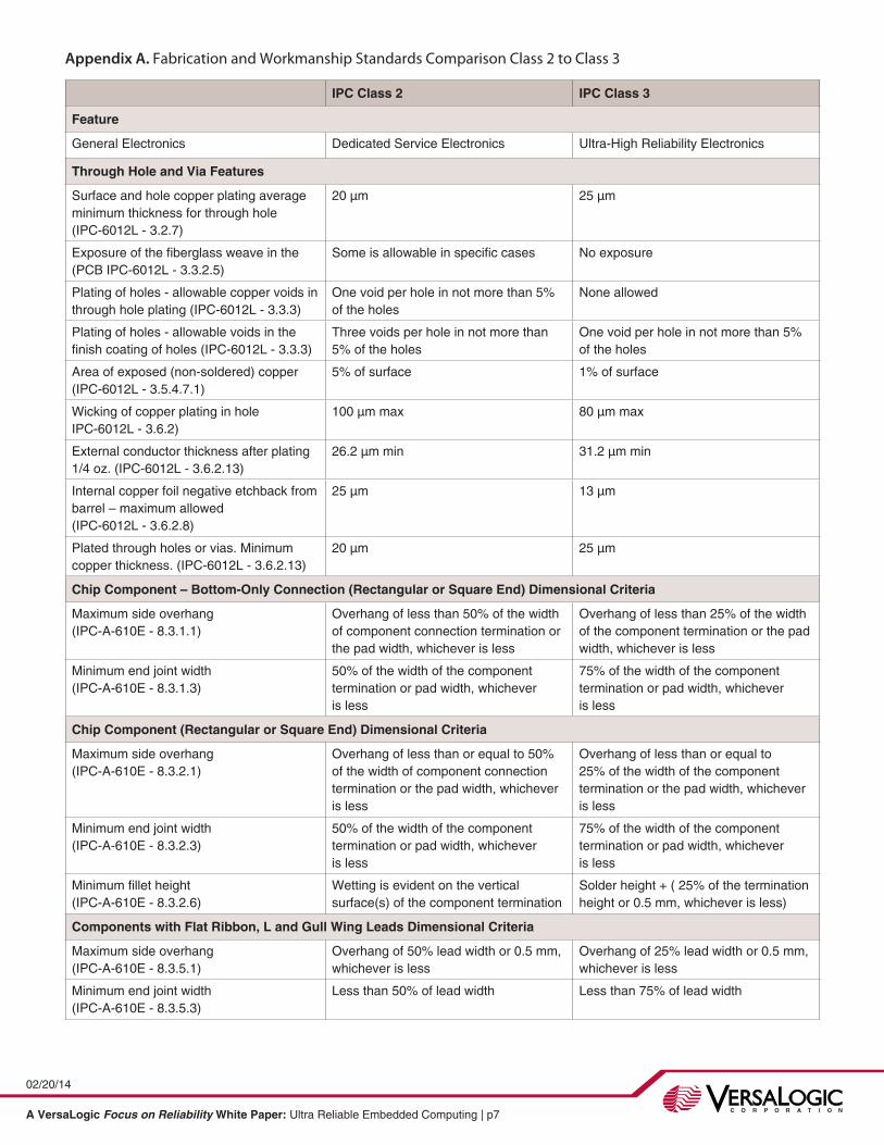
After experimenting with several other approaches, a solution was developed that reli-ably solved the challenge. It was a two piece solution that provides ultra reliable prod-ucts while supporting modern small geometry BGA chips. First is the use of a larger
8 mil mechanical drill for via holes to control drill wander and plating issues. Second is to change the standard circular annular rings to a slightly larger teardrop-shaped via pad (Figure 7).
The teardrop pad provides the necessary drill margin in the area of the neck where the trace meets the pad. In this design, even if the drill wanders closer to the neck of the pad, there is still a sufficient margin of copper between the hole and the edge of the pad to maintain a reliable connection. The use of the teardrop pad, along with tight manufacturing tolerances and controls used by VersaLogic, provide a reliable electrical and mechanical connection at each via. This combination of design and manufacturing expertise enables the production of a high reliability product, using the latest BGA packages.
A Comprehensive Approach to Ultra-High Reliability Embedded ComputersProducing ultra-high reliability embedded computers takes more than just innovative design techniques. A multi-faceted approach is needed to achieve the highest levels of reliability. Experienced design teams, superior supply chain management, leading-edge manufacturing, and stringent quality control processes are needed to realize the highest levels of product reliability. VersaLogic leverages state-of-the-art equipment and a wide array of design and manufacturing tools to achieve this goal. None of this matters if the underlying circuit board is impossible to manufacture or is not mechani-cally or electronically robust. Class 3 design and inspection standards, combined with modifications for current fine-pitch CPU chips, result in a best-in-class program for producing ultra-high reliability embedded computers.
A VersaLogic Focus on Reliability White Paper: Ultra Reliable Embedded Computing | p7 VERSALOGICC O R P O R A T I O N
Appendix A. Fabrication and Workmanship Standards Comparison Class 2 to Class 3
IPC Class 2 IPC Class 3
Feature
General Electronics Dedicated Service Electronics Ultra-High Reliability Electronics
Through Hole and Via Features
Surface and hole copper plating average minimum thickness for through hole (IPC-6012L - 3.2.7)
20 µm 25 µm
Exposure of the fiberglass weave in the (PCB IPC-6012L - 3.3.2.5)
Some is allowable in specific cases No exposure
Plating of holes - allowable copper voids in through hole plating (IPC-6012L - 3.3.3)
One void per hole in not more than 5% of the holes
None allowed
Plating of holes - allowable voids in the finish coating of holes (IPC-6012L - 3.3.3)
Three voids per hole in not more than 5% of the holes
One void per hole in not more than 5% of the holes
Area of exposed (non-soldered) copper (IPC-6012L - 3.5.4.7.1)
5% of surface 1% of surface
Wicking of copper plating in hole IPC-6012L - 3.6.2)
100 µm max 80 µm max
External conductor thickness after plating 1/4 oz. (IPC-6012L - 3.6.2.13)
26.2 µm min 31.2 µm min
Internal copper foil negative etchback from barrel – maximum allowed (IPC-6012L - 3.6.2.8)
25 µm 13 µm
Plated through holes or vias. Minimum copper thickness. (IPC-6012L - 3.6.2.13)
20 µm 25 µm
Chip Component – Bottom-Only Connection (Rectangular or Square End) Dimensional Criteria
Maximum side overhang (IPC-A-610E - 8.3.1.1)
Overhang of less than 50% of the width of component connection termination or the pad width, whichever is less
Overhang of less than 25% of the width of the component termination or the pad width, whichever is less
Minimum end joint width (IPC-A-610E - 8.3.1.3)
50% of the width of the component termination or pad width, whichever is less
75% of the width of the component termination or pad width, whichever is less
Chip Component (Rectangular or Square End) Dimensional Criteria
Maximum side overhang (IPC-A-610E - 8.3.2.1)
Overhang of less than or equal to 50% of the width of component connection termination or the pad width, whichever is less
Overhang of less than or equal to 25% of the width of the component termination or the pad width, whichever is less
Minimum end joint width (IPC-A-610E - 8.3.2.3)
50% of the width of the component termination or pad width, whichever is less
75% of the width of the component termination or pad width, whichever is less
Minimum fillet height (IPC-A-610E - 8.3.2.6)
Wetting is evident on the vertical surface(s) of the component termination
Solder height + ( 25% of the termination height or 0.5 mm, whichever is less)
Components with Flat Ribbon, L and Gull Wing Leads Dimensional Criteria
Maximum side overhang (IPC-A-610E - 8.3.5.1)
Overhang of 50% lead width or 0.5 mm, whichever is less
Overhang of 25% lead width or 0.5 mm, whichever is less
Minimum end joint width (IPC-A-610E - 8.3.5.3)
Less than 50% of lead width Less than 75% of lead width
02/20/14