ultra-flat platinum surfaces from template-stripping of sputter deposited films
TRANSCRIPT
Surface Science 546 (2003) 87–96
www.elsevier.com/locate/susc
Ultra-flat platinum surfaces from template-strippingof sputter deposited films
Jason J. Blackstock a,b,*, Zhiyong Li b, Mark R. Freeman a, Duncan R. Stewart b
a Department of Physics, P-412, Avadh Bhatia Physics Lab, University of Alberta, Edmonton, Canada T6G 2J1b Hewlett-Packard Laboratories, 1501 Page Mill Road, MS 1123, Palo Alto, CA 94304, USA
Received 4 July 2003; accepted for publication 30 September 2003
Abstract
We report the fabrication of platinum (Pt) surfaces with single-angstrom flatness by template-stripping sputtered
films from silicon wafers. For comparison, template-stripped (TS) gold (Au) is also produced from sputtered films using
the same procedure. The surface wetting properties, refractive indices and extinction coefficients of the TS platinum are
presented and compared against those of non-TS platinum films. The observed optical constants, as well as X-ray
crystallography data, suggest that macroscopic properties of the sputtered TS platinum films are similar to previously
studied evaporated platinum films [Surf. Interf. Anal. 29 (2000) 179]. Finally, scanning probe microscopy studies of the
topography of TS Pt and TS Au sputtered metal surfaces are presented. Immediately after stripping, the TS platinum
exhibits �1 �AA root-mean-square roughness over one square micron and demonstrates higher fidelity to the templatingsilicon wafer than TS gold. The TS platinum surface also shows high physical stability in ambient laboratory conditions
over the period of a week, whereas considerable topographical aging is observed in the case of the TS gold surface. The
results are discussed in relation to the potential of TS platinum for use in molecular electronic systems.
� 2003 Elsevier B.V. All rights reserved.
Keywords: Atomic force microscopy; Scanning tunneling microscopy; Metallic surfaces; Platinum; Gold
1. Introduction
Considerable attention has been directed in re-cent years towards the use of self-assembled
monolayers (SAMs) in molecular electronics. The
variety of methods employed to study the electrical
properties of these systems have included break-
* Corresponding author. Address: Department of Physics,
P-412, Avadh Bhatia Physics Lab, University of Alberta,
Edmonton, Canada T6G 2J1. Tel.: +1-780-718-6630; fax: +1-
780-492-0714.
E-mail address: [email protected] (J.J. Blackstock).
0039-6028/$ - see front matter � 2003 Elsevier B.V. All rights reservdoi:10.1016/j.susc.2003.09.039
junctions [2], nanopores [3], scanning tunnelling
microscopy (STM) and conduction probe atomic
force microscopy (cpAFM) [4–14], and more re-cently the chemical growth of monolayer junctions
in nanowires [15–17]. Throughout these wide-
ranging experiments, the focus has been almost
exclusively on gold as the surface for self-assem-
bly. This is easily understood as the gold Æ1 1 1æsurface is well studied, and there exists a wealth of
information on the behaviour of SAMs on gold,
discussed in several reviews [18–21]. Despite theconsiderable effort put into the study of gold as a
molecular electronics substrate however, gold is
essentially incompatible with silicon semiconductor
ed.
88 J.J. Blackstock et al. / Surface Science 546 (2003) 87–96
technologies due to its high diffusivity and elec-
tronic role as a mid-bandgap trap. Thus, without
considerable difficulty, gold can not be used for
the desired integration of molecular electronic cir-
cuitry with conventional electronics. In addition,
one study [14] has suggested that the linchpin ofmany SAMs––the gold–thiol bond––appears sub-
ject to intrinsic fluctuations; a so-called �blinking�effect.
One potential alternative substrate for molecu-
lar electronics is platinum [22], which has the sig-
nificant advantage over gold that it does not form
a deep electronic trap in silicon. In addition, the
transmittance of thiol-monolayer systems inter-faced with platinum have been observed to be
roughly two orders of magnitude higher than the
same monolayer systems interfaced with gold [23].
In a previous paper [24], the characteristics of
sputtered platinum surfaces treated with a variety
of processing plasmas were explored. Similar to
other metal films however, as-deposited platinum
displays considerable roughness on the molecularlength scale. Such roughness is a major challenge
in the fabrication of working SAM junctions, as
sharp features can cause defects in SAMs, leading
to electrical shorts across the junctions. In this
paper we report the fabrication and physical
characterization of clean platinum surfaces with
near atomic-scale smoothness over large areas
using a template-stripping [25] technique.Originally developed using mica as the templat-
ing surface, template-stripping has been shown to
produce gold surfaces with sub-nanometer flatness
over tens of square microns [26]. Template-stripped
(TS) Au has been used in numerous experiments,
ranging from the study of adsorbed molecules [26–
29] and biomolecules [30,31], to the study of the
Casimir force between parallel plates [32]. In addi-tion, the template-stripping method has been ex-
panded to utilize templating surfaces other than
mica [33,34], and has been applied to a few other
metals, including silver [34] and titanium (or tita-
nium-oxide) [35,36].
For our templating surfaces, prime polished
SiÆ1 0 0æ wafers with a thin oxide layer were em-ployed. Once stripped, the surface wetting prop-erties, as well as multi-wavelength measurements
of the refractive index and extinction coefficient
confirmed the cleanliness of the TS Pt surface,
including the absence of any surface platinum-
oxide or silicon-oxide layer. X-ray diffraction data
demonstrated that the sputtered TS Pt and TS Au
are predominantly Æ1 1 1æ oriented polycrystallinefilms, with bulk crystallite grain sizes in the tens ofnanometers for both metals. The optical and X-ray
data also demonstrated that the macroscopic sur-
face properties of the sputtered TS platinum films
are very similar to previously examined, evapo-
rated platinum films [1]. Last and most significant
are the scanning probe microscopy studies. A
systematic atomic force microscopy (AFM) study
of the surfaces revealed Pt surfaces with sub-ang-strom RMS roughness and excellent physical sta-
bility when exposed to ambient conditions for 1
week. In contrast, TS Au surfaces were consis-
tently rougher (>1 �AA RMS) and much less stable,roughening further up to 50% RMS over 1 week.
Scanning tunnelling microscopy (STM) images
obtained from both TS Pt and TS Au surfaces
confirmed the AFM observations, and also re-solved surface grain boundaries, revealing grain
sizes in good agreement with bulk grain sizes ex-
tracted from the X-ray diffraction data.
2. Experimental procedures
2.1. Sample preparation
The 400SiÆ1 0 0æ prime wafers with a native
thermal oxide layer (P-type; Boron doped; 1–20
X cm; Silicon Valley Microelectronics, CA) werefirst cleaned in piranha solution (a 1:3 by volume
mixture of 30% hydrogen peroxide and concen-
trated sulphuric acid) for fifteen minutes, removing
any organic contamination. Ellipsometric mea-surements showed that the piranha cleaning pro-
cedure also increased the thickness of the oxide
layer from �10 �AA to �15 �AA. Once removed fromthe piranha, wafers were rinsed thoroughly with
de-ionized water, dried under a stream of dry ni-
trogen, then placed immediately into the sputter-
ing chamber. Platinum and gold (both 99.99%)
were sputtered at 7 mTorr of argon backpressureonto different wafers at calibrated rates of 5 and 8
nm/min respectively, to total thicknesses of 100 nm

J.J. Blackstock et al. / Surface Science 546 (2003) 87–96 89
or greater. The presence of the thin silicon-oxide
was found necessary to prevent metal–silicon
bonding at the interfaces. For room temperature
depositions a thicker oxide was found not to be
necessary and was not used as the oxide growth
would increase the roughness of the prime SiÆ1 0 0æsurface.
Once the substrates were removed from the
sputtering chamber, square pieces of glass or sili-
con (roughly 1 cm2) were attached to the exposed
side of the Pt or Au surface using EPO-TEK 377 (a
two part epoxy that contains no solvent and is
resistant to many organic solvents, such as the
alcohols typically used in the deposition of mo-lecular monolayers; Epoxy Technologies, MA)
[25]. The epoxy was cured by placing the wafers in
an oven at 150 �C for 2 h. Once cured, the waferswere placed on the shelf until samples were re-
quired. From a single 400Si wafer, as many as
twenty to thirty 1 cm2 samples could be easily
obtained.
To �strip� a fresh sample from the wafer, a razorblade and metal tweezers were used. First, a sharp
razor blade was run around the edge of the sample
to separate the sample from excess epoxy on the
surface. Then, the point of the tweezers was gently
pushed under one corner of a sample and used to
pry the sample up. Samples stripped easily without
need for chemically assisted stripping [26], reduc-
ing contamination of the fresh surface. No differ-ences were observed between samples stripped
immediately after curing the epoxy and those
stripped after sitting on the shelf for a period up to
2 months.
2.2. Characterization
The static contact angle measurements wereperformed using a VCA 100 video contact angle
system (AST Products Inc., Billerica, MA) as de-
scribed previously [24]. Optical measurements
were made using a Gaertner ellipsometer (Gaert-
ner Scientific Corporation, Skokie, Il), operating
at an incident angle of 70� with three differentwavelengths (543.5, 632.8 and 832.2 nm). A simple
model built into the equipment software was usedto obtain the refractive index (n) and extinctioncoefficient (k) of the platinum samples, where the
thickness of the films (P1000 �AA) was more thansufficient to assume the ellipsometer was observing
only the films and not the underlying substrates;
an estimate of the penetration depth (d) calculatedfrom the equation d ¼ k
4p�k using measured values
of k yields depths in the vicinity of only 100 �AA. Aminimum of three TS Pt samples, measured at
multiple locations on each sample, were examined
for the ellipsometry measurements. The X-ray
crystallography was carried out using a Rigaku
Geigerflex 2173 (Rigaku/MSC, The Woodlands,
TX) operating with a cobalt X-ray source.
The atomic force microscopy (AFM) was car-
ried out in contact mode under ambient conditionsusing commercial Si3N4 cantilevers (ThermoMi-
croscope; 0.05–0.5 N/m; radius of curvature 6 20
nm) and digital instruments multi-mode and di-
mension 3000 microscopes. For the root-mean-
square (RMS) roughness and peak-to-valley (PV)
roughness values, several scans at random loca-
tions across at least two different samples were
taken with either 0.1 or 1 lm scan fields, and theembedded functions of the Digital Instruments
software were used to determine the sample
roughness of each scan (a first order flattening
followed by the roughness calculations). The in-
dependent values were then averaged and the
standard deviation taken as an estimate of the
error on the quoted values. Scanning tunneling
microscopy (STM) was carried out on a DigitalInstruments Multi-mode microscope using plati-
num–irridium tips (ThermoMicroscope).
3. Results
3.1. Surface wetting properties
The contact angle of a water droplet against a
surface is a measure of the surface hydrophilicity.
Previous experiments on clean platinum [37] and
gold [38] have both demonstrated a hydrophilic na-
ture (very low water contact angle, 620�), thoughwithin only minutes of exposure to ambient labo-
ratory conditions, both surfaces become increas-
ingly hydrophobic (water contact angle P30�).This change is attributed to adsorption of various
chemical species to the metal surfaces, indicating
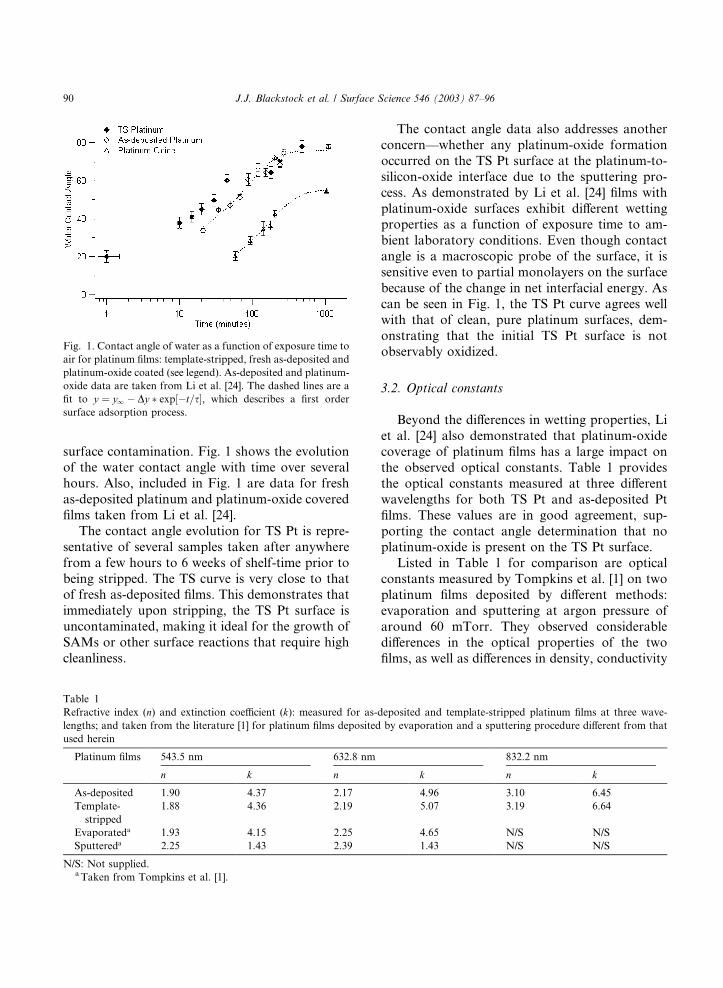
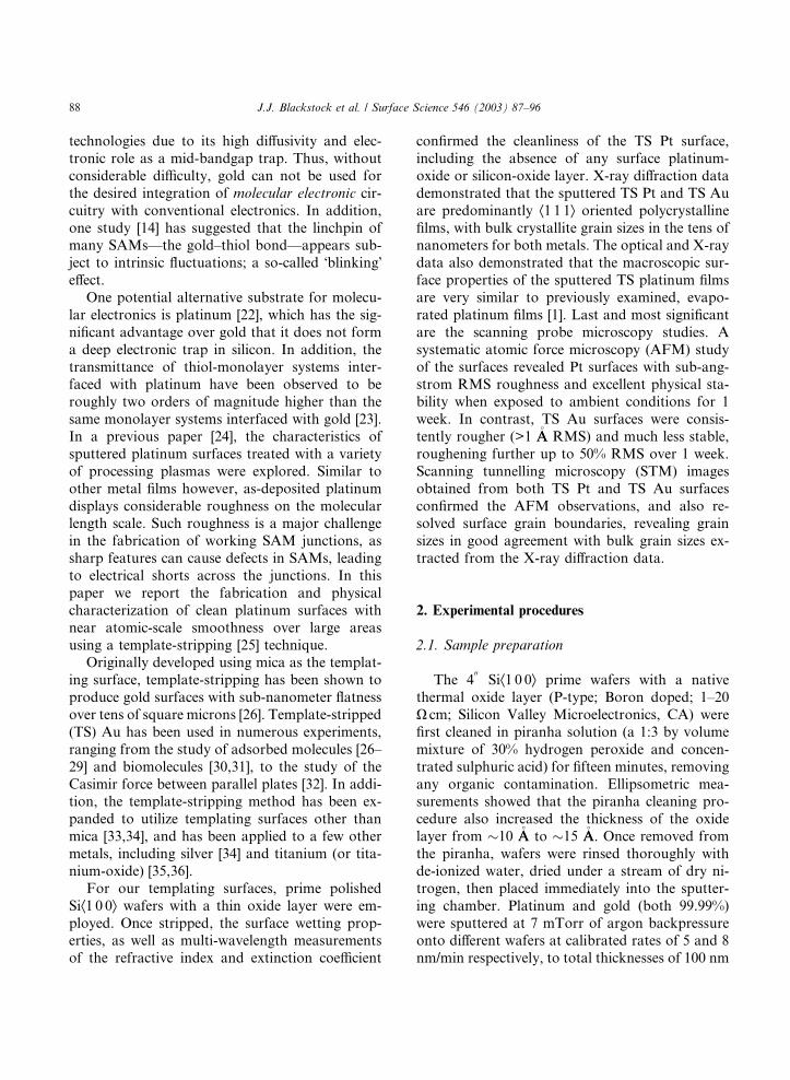
Fig. 1. Contact angle of water as a function of exposure time to
air for platinum films: template-stripped, fresh as-deposited and
platinum-oxide coated (see legend). As-deposited and platinum-
oxide data are taken from Li et al. [24]. The dashed lines are a
fit to y ¼ y1 � Dy � exp½�t=s, which describes a first ordersurface adsorption process.
90 J.J. Blackstock et al. / Surface Science 546 (2003) 87–96
surface contamination. Fig. 1 shows the evolutionof the water contact angle with time over several
hours. Also, included in Fig. 1 are data for fresh
as-deposited platinum and platinum-oxide covered
films taken from Li et al. [24].
The contact angle evolution for TS Pt is repre-
sentative of several samples taken after anywhere
from a few hours to 6 weeks of shelf-time prior to
being stripped. The TS curve is very close to thatof fresh as-deposited films. This demonstrates that
immediately upon stripping, the TS Pt surface is
uncontaminated, making it ideal for the growth of
SAMs or other surface reactions that require high
cleanliness.
Table 1
Refractive index (n) and extinction coefficient (k): measured for as-dlengths; and taken from the literature [1] for platinum films deposited
used herein
Platinum films 543.5 nm 632.8 nm
n k n
As-deposited 1.90 4.37 2.17
Template-
stripped
1.88 4.36 2.19
Evaporateda 1.93 4.15 2.25
Sputtereda 2.25 1.43 2.39
N/S: Not supplied.a Taken from Tompkins et al. [1].
The contact angle data also addresses another
concern––whether any platinum-oxide formation
occurred on the TS Pt surface at the platinum-to-
silicon-oxide interface due to the sputtering pro-
cess. As demonstrated by Li et al. [24] films with
platinum-oxide surfaces exhibit different wettingproperties as a function of exposure time to am-
bient laboratory conditions. Even though contact
angle is a macroscopic probe of the surface, it is
sensitive even to partial monolayers on the surface
because of the change in net interfacial energy. As
can be seen in Fig. 1, the TS Pt curve agrees well
with that of clean, pure platinum surfaces, dem-
onstrating that the initial TS Pt surface is notobservably oxidized.
3.2. Optical constants
Beyond the differences in wetting properties, Li
et al. [24] also demonstrated that platinum-oxide
coverage of platinum films has a large impact on
the observed optical constants. Table 1 provides
the optical constants measured at three different
wavelengths for both TS Pt and as-deposited Pt
films. These values are in good agreement, sup-
porting the contact angle determination that noplatinum-oxide is present on the TS Pt surface.
Listed in Table 1 for comparison are optical
constants measured by Tompkins et al. [1] on two
platinum films deposited by different methods:
evaporation and sputtering at argon pressure of
around 60 mTorr. They observed considerable
differences in the optical properties of the two
films, as well as differences in density, conductivity
eposited and template-stripped platinum films at three wave-
by evaporation and a sputtering procedure different from that
832.2 nm
k n k
4.96 3.10 6.45
5.07 3.19 6.64
4.65 N/S N/S
1.43 N/S N/S
J.J. Blackstock et al. / Surface Science 546 (2003) 87–96 91
and X-ray diffraction data. For the platinum films
in this report, the argon pressure used during for
sputtering was considerably lower (7 mTorr),
which Tompkins et al. point out can be reasonably
expected to produce film structure closer to that of
evaporated films. Comparing the optical constantsof the platinum films examined herein to the
Tompkins et al. data at both 543.5 and 642.8 nm,
it is apparent that the optical properties of our
sputtered films are similar to those of their evap-
orated films and quite different from their sput-
tered films.
3.3. X-ray diffraction
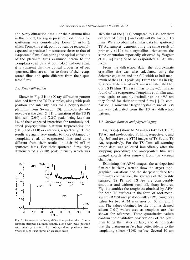
Shown in Fig. 2 is the X-ray diffraction pattern
obtained from the TS Pt samples, along with peak
position and intensity bars for a polycrystalline
platinum from Swanson [39]. Immediately ob-
servable is the clear Æ1 1 1æ orientation of the TS Ptfilm, with Æ2 0 0æ and Æ2 2 0æ peaks being less than1% of their expected intensities for randomly ori-ented polycrystalline platinum (representing the
Æ1 0 0æ and Æ1 1 0æ orientations, respectively). Theseresults are again very similar to those obtained by
Tompkins et al. on evaporated films, and quite
different from their results on their 60 mTorr
sputtered films. For their sputtered films, they
demonstrated a Æ2 0 0æ peak intensity which was
Fig. 2. Representative X-ray diffraction profile taken from a
template-stripped platinum sample, along with peak position
and intensity markers for polycrystalline platinum from
Swanson [39]. Inset shows an enlarged scale.
16% that of the Æ1 1 1æ compared to 1.4% for theirevaporated films [1] and only �0.4% for our TSfilms. We also obtained similar data for sputtered
TS Au samples, demonstrating the same result of
primarily Æ1 1 1æ bulk crystallite orientation; thesame orientation reportedly observed by Wagneret al. [26] using STM on evaporated TS Au sur-
faces.
From the diffraction data, the approximate
crystallite size was also calculated using the
Scherrer equation and the full-width-at-half-max-
imum of the Æ1 1 1æ peak [40]. From the data in Fig.2, a crystallite size of �21 nm was calculated forour TS Pt films. This is similar to the �25 nm sizefound of the evaporated Tompkins et al. film and,
once again, reasonably dissimilar to the �9.5 nmthey found for their sputtered films [1]. In com-
parison, a somewhat larger crystallite size of �38nm was calculated from the TS Au diffraction
pattern.
3.4. Surface flatness and physical aging
Fig. 3(a)–(c) show AFM images taken of TS Pt,
TS Au and as-deposited Pt films, respectively, and
Fig. 3(d) and (e) are STM images of TS Pt and TS
Au, respectively. For the TS films, all scanning
probe data was collected immediately after the
stripping procedure; the as-deposited film was
imaged shortly after removal from the vacuumchamber.
Examining the AFM images, the as-deposited
film can be clearly seen to show the largest topo-
graphical variations and the sharpest surface fea-
tures––by comparison, the surfaces of the freshly
stripped TS Pt and TS Au are considerably
smoother and without such tall, sharp features.
Fig. 4 quantifies the roughness obtained by AFMfor both TS surfaces in the form of root-mean-
square (RMS) and peak-to-valley (PV) roughness
values for two AFM scan sizes of 100 nm and 1
lm. The values obtained for the piranha cleanedsilicon Æ1 0 0æ wafers used as templates are alsoshown for reference. These quantitative values
confirm the qualitative observations of the plati-
num being the flatter surface, and demonstratethat the platinum in fact has better fidelity to the
templating silicon Æ1 0 0æ surface. Several 10 lm
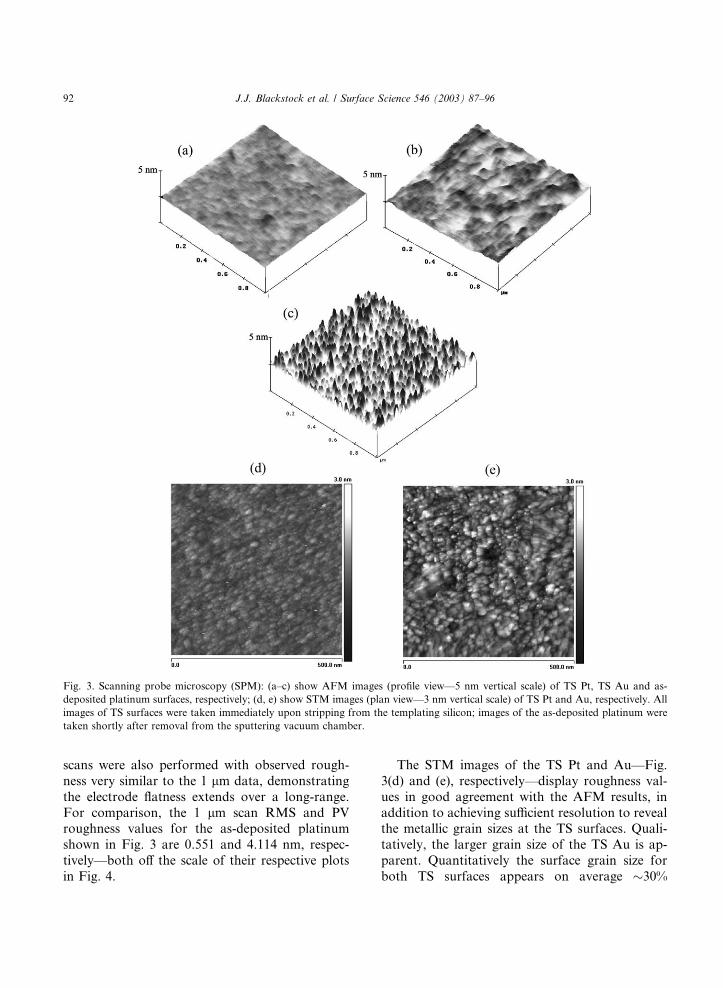
Fig. 3. Scanning probe microscopy (SPM): (a–c) show AFM images (profile view––5 nm vertical scale) of TS Pt, TS Au and as-
deposited platinum surfaces, respectively; (d, e) show STM images (plan view––3 nm vertical scale) of TS Pt and Au, respectively. All
images of TS surfaces were taken immediately upon stripping from the templating silicon; images of the as-deposited platinum were
taken shortly after removal from the sputtering vacuum chamber.
92 J.J. Blackstock et al. / Surface Science 546 (2003) 87–96
scans were also performed with observed rough-
ness very similar to the 1 lm data, demonstratingthe electrode flatness extends over a long-range.
For comparison, the 1 lm scan RMS and PVroughness values for the as-deposited platinum
shown in Fig. 3 are 0.551 and 4.114 nm, respec-
tively––both off the scale of their respective plots
in Fig. 4.
The STM images of the TS Pt and Au––Fig.
3(d) and (e), respectively––display roughness val-
ues in good agreement with the AFM results, in
addition to achieving sufficient resolution to revealthe metallic grain sizes at the TS surfaces. Quali-
tatively, the larger grain size of the TS Au is ap-
parent. Quantitatively the surface grain size for
both TS surfaces appears on average �30%
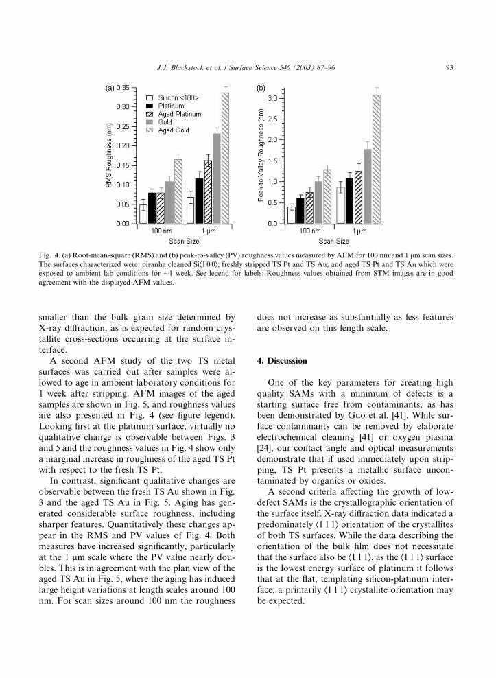
Fig. 4. (a) Root-mean-square (RMS) and (b) peak-to-valley (PV) roughness values measured by AFM for 100 nm and 1 lm scan sizes.The surfaces characterized were: piranha cleaned SiÆ1 0 0æ; freshly stripped TS Pt and TS Au; and aged TS Pt and TS Au which wereexposed to ambient lab conditions for �1 week. See legend for labels. Roughness values obtained from STM images are in goodagreement with the displayed AFM values.
J.J. Blackstock et al. / Surface Science 546 (2003) 87–96 93
smaller than the bulk grain size determined byX-ray diffraction, as is expected for random crys-
tallite cross-sections occurring at the surface in-
terface.
A second AFM study of the two TS metal
surfaces was carried out after samples were al-
lowed to age in ambient laboratory conditions for
1 week after stripping. AFM images of the aged
samples are shown in Fig. 5, and roughness valuesare also presented in Fig. 4 (see figure legend).
Looking first at the platinum surface, virtually no
qualitative change is observable between Figs. 3
and 5 and the roughness values in Fig. 4 show only
a marginal increase in roughness of the aged TS Pt
with respect to the fresh TS Pt.
In contrast, significant qualitative changes are
observable between the fresh TS Au shown in Fig.3 and the aged TS Au in Fig. 5. Aging has gen-
erated considerable surface roughness, including
sharper features. Quantitatively these changes ap-
pear in the RMS and PV values of Fig. 4. Both
measures have increased significantly, particularly
at the 1 lm scale where the PV value nearly dou-bles. This is in agreement with the plan view of the
aged TS Au in Fig. 5, where the aging has inducedlarge height variations at length scales around 100
nm. For scan sizes around 100 nm the roughness
does not increase as substantially as less featuresare observed on this length scale.
4. Discussion
One of the key parameters for creating high
quality SAMs with a minimum of defects is a
starting surface free from contaminants, as hasbeen demonstrated by Guo et al. [41]. While sur-
face contaminants can be removed by elaborate
electrochemical cleaning [41] or oxygen plasma
[24], our contact angle and optical measurements
demonstrate that if used immediately upon strip-
ping, TS Pt presents a metallic surface uncon-
taminated by organics or oxides.
A second criteria affecting the growth of low-defect SAMs is the crystallographic orientation of
the surface itself. X-ray diffraction data indicated a
predominately Æ1 1 1æ orientation of the crystallitesof both TS surfaces. While the data describing the
orientation of the bulk film does not necessitate
that the surface also be Æ1 1 1æ, as the Æ1 1 1æ surfaceis the lowest energy surface of platinum it follows
that at the flat, templating silicon-platinum inter-face, a primarily Æ1 1 1æ crystallite orientation maybe expected.
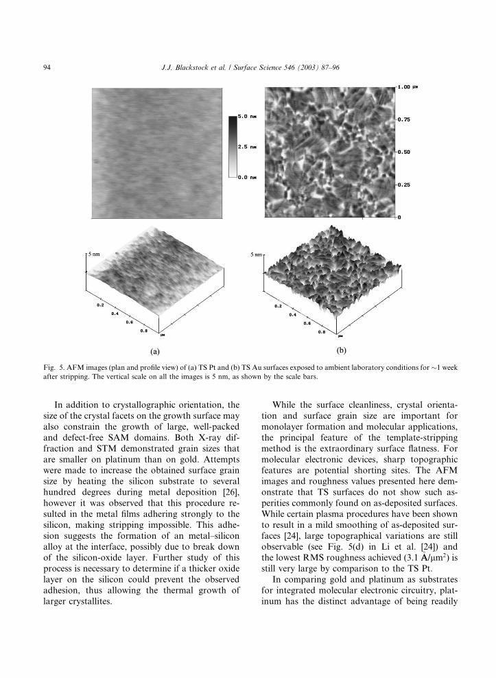
Fig. 5. AFM images (plan and profile view) of (a) TS Pt and (b) TS Au surfaces exposed to ambient laboratory conditions for �1 weekafter stripping. The vertical scale on all the images is 5 nm, as shown by the scale bars.
94 J.J. Blackstock et al. / Surface Science 546 (2003) 87–96
In addition to crystallographic orientation, the
size of the crystal facets on the growth surface may
also constrain the growth of large, well-packed
and defect-free SAM domains. Both X-ray dif-
fraction and STM demonstrated grain sizes that
are smaller on platinum than on gold. Attemptswere made to increase the obtained surface grain
size by heating the silicon substrate to several
hundred degrees during metal deposition [26],
however it was observed that this procedure re-
sulted in the metal films adhering strongly to the
silicon, making stripping impossible. This adhe-
sion suggests the formation of an metal–silicon
alloy at the interface, possibly due to break downof the silicon-oxide layer. Further study of this
process is necessary to determine if a thicker oxide
layer on the silicon could prevent the observed
adhesion, thus allowing the thermal growth of
larger crystallites.
While the surface cleanliness, crystal orienta-
tion and surface grain size are important for
monolayer formation and molecular applications,
the principal feature of the template-stripping
method is the extraordinary surface flatness. For
molecular electronic devices, sharp topographicfeatures are potential shorting sites. The AFM
images and roughness values presented here dem-
onstrate that TS surfaces do not show such as-
perities commonly found on as-deposited surfaces.
While certain plasma procedures have been shown
to result in a mild smoothing of as-deposited sur-
faces [24], large topographical variations are still
observable (see Fig. 5(d) in Li et al. [24]) andthe lowest RMS roughness achieved (3.1 �AA/lm2) isstill very large by comparison to the TS Pt.
In comparing gold and platinum as substrates
for integrated molecular electronic circuitry, plat-
inum has the distinct advantage of being readily

J.J. Blackstock et al. / Surface Science 546 (2003) 87–96 95
compatible with silicon microelectronics. From
this study, we can see that there are additional
advantages to platinum over gold. TS Pt was
shown to have a flatter surface than TS Au, more
faithful to the templating oxidized silicon surface.
This can be understood by considering the meltingpoints (Au: 1064 �C, Pt: 1768 �C), and the corre-sponding malleabilities of the two metals at am-
bient temperatures at which the stripping takes
place; gold is the softer of the two metals and any
stress induced in the films during the stripping
procedure will hence cause more distortion in the
gold films than in the platinum.
The hardness difference between the two metalsalso influences the physical aging of the two TS
surfaces. Previous STM studies have demonstrated
that at room temperature, freshly-prepared atom-
ically flat gold Æ1 1 1æ surfaces are mobile enoughthat they undergo almost continuous reconstruc-
tion [42]. Fig. 5 demonstrates that similar recon-
struction of the TS Au has occurred over the
period of 1 week under ambient conditions. Incontrast, the platinum surfaces show almost no
change over the same period, as the refractory
nature of the platinum provides a higher stability
surface. This increased stability could be a signi-
ficant factor in molecular electronic systems for
three reasons. First, high stability means higher
resistance to thermal aging of devices at ambient
conditions and thus higher resistance to devicefailure––especially with added stresses from elec-
trical cycling. Secondly, a harder surface may limit
or eliminate the presence of the etch-pits com-
monly observed on gold–thiol systems [43–46]
which contribute to monolayer defects and thus
potential shorting sites. Third, the stochastic mo-
lecular conductance switching observed by Do-
nhauser et al. [7] and Ramachandran et al. [14]with Au-thiol monolayers has recently been at-
tributed to Au–Au bond fluctuations at the thiol
anchor site [14]. The higher melting point of plati-
num and evidenced stability of the platinum surface
are both demonstrations that the platinum–plati-
num bond is considerably stronger than the gold-
gold bond. If a weak Au–Au bond is the origin of
the observed fluctuations, the stronger platinum–platinum bond should reduce, if not eliminate, the
stochastic conductance switching.
5. Conclusions
In this paper we have demonstrated that ultra-
flat platinum surfaces can be prepared by the
template-stripping of sputtered platinum filmsfrom silicon Æ1 0 0æ surfaces. Surface contact angleand optical measurements indicated the template
stripped surfaces were as clean as freshly vacuum
deposited Pt. X-ray diffraction illustrated that the
TS Pt thin films consisted of �21 nm Æ1 1 1æ ori-ented crystallites. AFM and STM characterization
revealed an extremely flat surface up to length
scales of 10 lm, with high fidelity to the Si wafertemplate, and little change after exposure to am-
bient. In comparison, similarly prepared gold
surfaces demonstrated higher roughness and much
less stability, exhibiting considerable surface re-
construction. These results, combined with silicon
microelectronics compatibility and the high elec-
trical transmittance of platinum-monolayer sys-
tems [23], suggest that TS Pt may be ideally suitedfor use in monolayer-based molecular electronic
applications. The formation of molecular mono-
layers on the TS Pt and TS Au surfaces is currently
under investigation.
Acknowledgements
The authors would like to gratefully acknowl-
edge the assistance of Professor J.-B. Green and
Diane Kaird at the University of Alberta, as well
as T. Ha and X. Li at HP Labs, Palo Alto. The
authors also extend thanks to the University of
Alberta�s Nanofabrication Facility staff (particu-larly Stephanie Bozic and Mirwais Aktary) for
their help with equipment training and processdevelopment. JJB and MRF kindly thank NSERC
and iCORE for funding. DARPA funding for
work carried out at Hewlett-Packard Laboratories
is gratefully acknowledged.
References
[1] H.G. Tompkins, S. Tasic, J. Baker, D. Convey, Surf.
Interf. Anal. 29 (2000) 179–187.
[2] M.A. Reed, C. Zhou, C.J. Muller, T.P. Burgin, J.M. Tour,
Science 278 (1997) 252–254.
96 J.J. Blackstock et al. / Surface Science 546 (2003) 87–96
[3] J. Chen, M.A. Reed, A.M. Rawlett, J.M. Tour, Science 286
(1999) 1550–1552.
[4] T.W. Kelley, E.L. Granstrom, C.D. Frisbie, Adv. Mater.
11 (1999) 261.
[5] D.J. Wold, C.D. Frisbie, J. Am. Chem. Soc. 122 (2000)
2970–2971.
[6] X.D. Cui, A. Primak, X. Zarate, J. Tomfohr, O.F. Sankey,
A.L. Moore, T.A. Moore, D. Gust, G. Harris, S.M.
Lindsay, Science 294 (2001) 571–574.
[7] Z.J. Donhauser, B.A. Mantooth, K.F. Kelly, L.A. Bumm,
J.D. Monnell, J.J. Stapleton, D.W. Price, A.M. Rawlett,
D.L. Allara, J.M. Tour, P.S. Weiss, Science 292 (2001)
2303–2307.
[8] D.J. Wold, C.D. Frisbie, J. Am. Chem. Soc 123 (2001)
5549–5556.
[9] X.D. Cui, A. Primak, X. Zarate, J. Tomfohr, O.F. Sankey,
A.L. Moore, T.A. Moore, D. Gust, L.A. Nagahara, S.M.
Lindsay, J. Phys. Chem. B 106 (2002) 8609–8614.
[10] X.D. Cui, X. Zarate, J. Tomfohr, A. Primak, A.L. Moore,
T.A. Moore, D. Gust, G. Harris, O.F. Sankey, S.M.
Lindsay, Ultramicroscopy 92 (2002) 67–76.
[11] X.D. Cui, X. Zarate, J. Tomfohr, O.F. Sankey, A. Primak,
A.L. Moore, T.A. Moore, D. Gust, G. Harris, S.M.
Lindsay, Nanotechnology 13 (2002) 5–14.
[12] A.M. Rawlett, T.J. Hopson, L.A. Nagahara, R.K. Tsui,
G.K. Ramachandran, S.M. Lindsay, Appl. Phys. Lett. 81
(2002) 3043–3045.
[13] D.J. Wold, R. Haag, M.A. Rampi, C.D. Frisbie, J. Phys.
Chem. B 106 (2002) 2813–2816.
[14] G.K. Ramachandran, T.J. Hopson, A.M. Rawlett, L.A.
Nagahara, A. Primak, S.M. Lindsay, Science 300 (2003)
1413.
[15] N.I. Kovtyukhova, B.R. Martin, J.K.N. Mbindyo, P.A.
Smith, B. Razavi, T.S. Mayer, T.E. Mallouk, J. Phys.
Chem. B 105 (2001) 8762–8769.
[16] I. Kratochvilova, M. Kocirik, A. Zambova, J. Mbindyo,
T.E. Mallouk, T.S. Mayer, J. Mater. Chem 12 (2002) 2927–
2930.
[17] J.K.N. Mbindyo, J.B. Mallouk, T.E. Mattzela, I. Krat-
ochvilova, B. Razavi, T.N. Jackson, T.S. Mayer, J. Am.
Chem. Soc. 124 (2002) 4020–4026.
[18] F. Schreiber, Prog. Surf. Sci. 65 (2000) 151–256.
[19] S.Y. Jiang, Mol. Phys. 100 (2002) 2261–2275.
[20] J.J. Gooding, F. Mearns, W.R. Yang, J.Q. Liu, Electro-
analysis 15 (2003) 81–96.
[21] D.K. Schwartz, Annu. Rev. Phys. Chem. 52 (2001) 107–137.
[22] Y. Chen, D.A.A. Ohlberg, X.M. Li, D.R. Stewart, R.S.
Williams, J.O. Jeppesen, K.A. Nielsen, J.F. Stoddart, D.L.
Olynick, E. Anderson, Appl. Phys. Lett. 82 (2003) 1610–
1612.
[23] J.M. Beebe, V.B. Engelkes, L.L. Miller, C.D. Frisbie, J.
Am. Chem. Soc. 124 (2002) 11268–11269.
[24] Z. Li, P. Beck, D.A.A. Ohlberg, D.R. Stewart, R.S.
Williams, Surf. Sci. 529 (2003) 410–418.
[25] M. Hegner, P. Wagner, G. Semenza, Surf. Sci. 291 (1993)
39–46.
[26] P. Wagner, M. Hegner, H.J. Guntherodt, G. Smemnza,
Langmuir 11 (1995) 3867–3875.
[27] S.S. Wong, M.D. Porter, J. Electroanal. Chem. 485 (2000)
135–143.
[28] Y.W. Huang, V.K. Gupta, Macromolecules 34 (2001)
3757–3764.
[29] Y.W. Huang, V.K. Gupta, Langmuir 18 (2002) 2280–2287.
[30] P. Wagner, F. Zaugg, P. Kernen, M. Hegner, G. Semenza,
J. Vac. Sci. Technol. B (1996).
[31] C.W. Ge, J.H. Liao, W. Yu, N. Gu, Biosens. Bioelectron.
18 (2003) 53–58.
[32] T. Ederth, Phys. Rev. A 14 (2000) 1466–1471.
[33] D. Stamou, D. Gourdon, M. Liley, N.A. Burnham, A.
Kulik, H. Vogel, C. Duschl, Langmuir 13 (1997) 2425–
2428.
[34] J. Diebel, H. Lowe, P. Samori, J.P. Rabe, Appl. Phys. A:
Mater. Sci. Process. 73 (2001) 273–279.
[35] P. Cacciafesta, K.R.O.C.A. Hallam, A.D.L. Humphris,
M.J. Miles, K.D. Jandt, Chem. Mater. 14 (2002) 777–789.
[36] K. Unal, B.O. Aronsson, Y. Mugnier, P. Descouts, Surf.
Interf. Sci. 34 (2002) 490–493.
[37] S. Guo, E. Hedborg, I. Lundstrom, H. Arwin, Thin Solid
Films 293 (1997) 179–184.
[38] T. Smith, Interf. Sci. 75 (1980) 51–55.
[39] T. Swanson, Natl. Bureau Stand. (U.S.) 539 (Circ.) (1953)
I31.
[40] B.D. Cullity, S.R. Stock, in: Elements of X-ray Diffraction,
third ed., Prentice Hall, Inc., Upper Saddle River, New
Jersey, 2001, pp. 167–171.
[41] L.-H. Guo, J.S. Facci, G. McLendon, R. Mosher, Lang-
muir 10 (1994) 4588–4593.
[42] N. Shimoni, S. Ayal, O. Millo, Phys. Rev. B 62 (2000) 147–
152.
[43] T. Han, T.P. Beebe, Langmuir 10 (1994) 2705–2709.
[44] C. Schonenberger, J.A.M. Sondaghuethorst, J. Jorritsma,
L.G.J. Fokkink, Langmuir 10 (1994) 611–614.
[45] R.L. McCarley, D.J. Dunaway, R.J. Willicut, Langmuir 9
(1993) 2775–2777.
[46] J.A.M. Sondaghuethorst, C. Schonenberger, L.G.J. Fok-
kink, J. Phys. Chem. 98 (1994) 6826–6834.