ug332: class 3 non-isolated evaluation board for the si3406 fileug332: class 3 non-isolated...
TRANSCRIPT

UG332: Class 3 Non-Isolated EvaluationBoard for the Si3406
The Si3406 non-isolated Flyback topology based evaluation boardis a reference design for a power supply in a Power over Ethernet(PoE) Powered Device (PD) application.This Si3406-non-ISO-FB EVB maximum output level is Class 3 power (η x 15.4 W).
The Si3406-non-ISO-FB EVB board is shown below. The Si3406 IC integrates an IEEE802.03at compatible PoE interface as well as a current control based dc/dc converter.The Si3406 PD integrates two diode bridges, which can be used up to 200 mA input cur-rent, detection circuit, classification circuit, dc/dc switch, hot-swap switch, TVS overvolt-age protection, dynamic soft-start circuit, cycle-by-cycle current limit, syncrhonous gatedriver, maintain power signature (MPS), thermal shutdown and inrush current protection.
The switching frequency of the converter is tunable by an external resistor.
KEY FEATURES
• IEEE 802.03at Compatible• High Efficiency• High Integration• Optional MPS Function• Synchronous Gate Driver• Low BOM Cost• Transient Overvoltage Protection• Thermal Shutdown Protection• 5x5 mm 20-pin QFN
silabs.com | Building a more connected world. Rev. 0.1
1. Kit Description
The Si3406-non-isolated Flyback topology based evaluation board is a reference design for power supplies in Power over Ethernet(PoE) Powered Device (PD) applications. The Si3406 device is described more completely in the data sheet and application notes. Thisdocument describes the evaluation board.
The Si3406-non-ISO-FB-C3 EVB board is shown on the cover page. The schematic is shown in Figure 2.3 Si3406-Non-Isolated Fly-back EVB Schematic: 5 V, Class 3 PD on page 4, and the layout is in 17. Board Layout. The dc output is at connectors J11(+) andJ12(–).
Boards are shipped configured to produce 5 V output voltage but can be configured for different output voltages, such as 3.3 or 12 V,by changing resistor R14 and a few other components. Refer to “AN1130: Using the Si3406/Si34061/Si34062 PoE+ and Si3404 PoEPD Controller in Isolated and Non-Isolated Designs” for more information. The preconfigured Class 3 signature can also be modified,which is described as well in AN1130.
The Si3406 includes integrated diode bridge for both CT and SP connection. The integrated diode bridge can be used up to 200 mAinput current. Above 200 mA input current the external diode bridge is required.
The external diode bridge can be Schottky or silicon type.
The Si3406 device can operate with CT/SP pins open, in this configuration the external bridge should be Schottky type diode bridge.
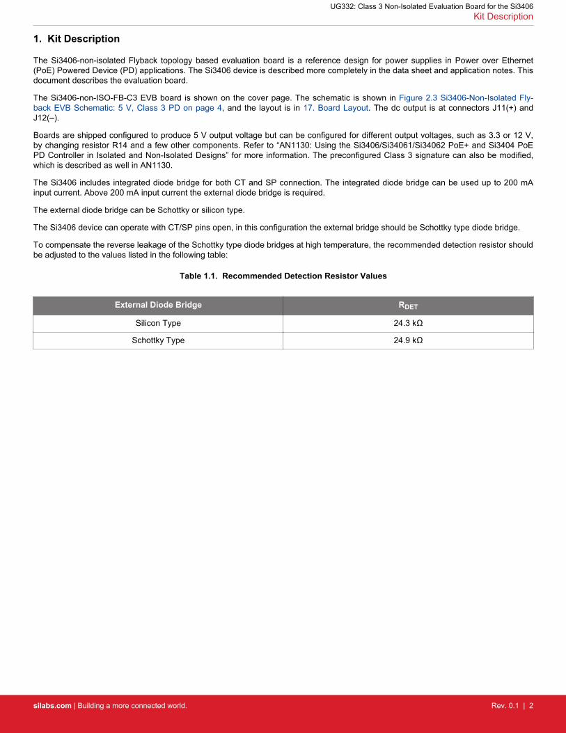
To compensate the reverse leakage of the Schottky type diode bridges at high temperature, the recommended detection resistor shouldbe adjusted to the values listed in the following table:
Table 1.1. Recommended Detection Resistor Values
External Diode Bridge RDET
Silicon Type 24.3 kΩ
Schottky Type 24.9 kΩ
UG332: Class 3 Non-Isolated Evaluation Board for the Si3406Kit Description
silabs.com | Building a more connected world. Rev. 0.1 | 2

2. Getting Started: Powering Up the Si3406-non-ISO-FB EVB
Ethernet data and power are applied to the board through the RJ45 connector (J1). The board itself has no Ethernet data transmissionfunctionality, but, as a convenience, the Ethernet transformer secondary-side data is brought out to test points.
The design can be used in Gigabit (10/100/1000) systems as well by using PoE RJ45 Magjack, such as type L8BE-1G1T-BFH from BelFuse.
Power may be applied in the following ways:• Using an IEEE 802.3-2015-compliant, PoE-capable PSE, such as Trendnet TPE-1020WS• Using a laboratory power supply unit (PSU):
• Connecting a dc source between blue/white-blue and brown/white-brown of the Ethernet cable (either polarity), (End-span) asshown below:
Figure 2.1. Endspan Connection using Laboratory Power Supply
• Connecting a dc source between green/white-green and orange/white-orange of the Ethernet cable (either polarity), (Mid-span)as shown below:
Figure 2.2. Midspan Connection using Laboratory Power Supply
UG332: Class 3 Non-Isolated Evaluation Board for the Si3406Getting Started: Powering Up the Si3406-non-ISO-FB EVB
silabs.com | Building a more connected world. Rev. 0.1 | 3

L5
330
Ohm
C6100uF
R2047K
J11
D19
S1B
TP4 NI
D12
S1B
T1
FA2924
29
178
10
J12
R14
9.1K
TP9vssNI
R21
0
R56.8
R15
3.24
K
TP5 NI
C16
1nF
NI
R10 48.7
C321nF
J1
RJ-45
MX0+1
MX0-3
MX1+4
PW
R2
8
PW
R3
9
PW
R4
10
CT2
LED
_K2
K2
LED
_A2
A2
LED
_K1
K1
LED
_A1
A1
PWR17
CT/MX1-5
MX1-6
PW
R5
11
C10
1uF
Q1FDMA8051LTP6 NI
C17
1nF
NI
R130.62
C201nF
C9
100u
F
NI
C12
1nF
NI
C40.01uF
+ C212uF
C13
1nF
NI
TP7 NI
C18
1nF
NI
R8 88.7K
C12.2uF
C14
1nF
NI
TP3 NI
C80.1uF
TP10swoNI
D18
S1B
L4
330
Ohm
C51nF
+
C7
220u
F
D15
S1B
TP1
vpos
NI
TP8 NI
TP2syncl
NI
U1
Si3406
FB
H1
ER
OU
T2
FB
L3
VD
D4
NSLEEP5
RDET6
HSO7
RCL8
RFREQ9
SP210
SP
111
VP
OS
12
CT
213
CT
114
NT2P15
SYNCL16
V1117
SWO18
VSS19
ISNS20
VN
EG
21
L1
330
Ohm
R2330
R11 24.3k
C19
1nF
NI
D51N4148W
NI
C15
1nF
NI
D17
S1B
C31
NI
C32.2uF
C22
0.1uF
D14
S1B
L2
330
Ohm
R1330
C11
100u
F
NI
R427k
L31uH
TP12
vneg
NI
D4RS1B
D16
S1B
C210.22uF
D13
S1B
swo
vpos vss
v11
fbl
nt2p
nt2p
vdd
Vss
vout
vss
vpos
vneg
vout
gnds
vdd
vss
vpos
erou
t
isns
vneg
vpos
vpos
ct2 ct
1
sp2
sp1
vss
vss gnds
Figure 2.3. Si3406-Non-Isolated Flyback EVB Schematic: 5 V, Class 3 PD
UG332: Class 3 Non-Isolated Evaluation Board for the Si3406Getting Started: Powering Up the Si3406-non-ISO-FB EVB
silabs.com | Building a more connected world. Rev. 0.1 | 4
3. Overall EVB Efficiency
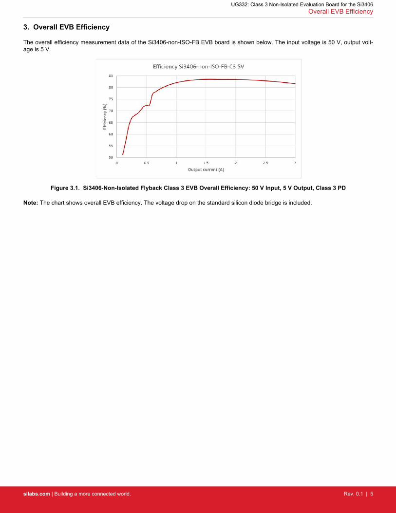
The overall efficiency measurement data of the Si3406-non-ISO-FB EVB board is shown below. The input voltage is 50 V, output volt-age is 5 V.
Figure 3.1. Si3406-Non-Isolated Flyback Class 3 EVB Overall Efficiency: 50 V Input, 5 V Output, Class 3 PD
Note: The chart shows overall EVB efficiency. The voltage drop on the standard silicon diode bridge is included.
UG332: Class 3 Non-Isolated Evaluation Board for the Si3406Overall EVB Efficiency
silabs.com | Building a more connected world. Rev. 0.1 | 5

4. SIFOS PoE Compatibility Test Results
The Si3406-non-ISO-FB EVB board has been successfully tested with PDA-300 Powered Device Analyzer from SIFOS Technologies.The PDA-300 Powered Device Analyzer is a single-box comprehensive solution for testing IEEE 802.3at PoE Powered Devices (PDs).
Figure 4.1. Si3406-Non-Isolated Flyback C3 PD SIFOS PoE Compatibility Test Results
UG332: Class 3 Non-Isolated Evaluation Board for the Si3406SIFOS PoE Compatibility Test Results
silabs.com | Building a more connected world. Rev. 0.1 | 6

5. Feedback Loop Phase and Gain Measurement Results (Bode Plots)
The Si3406 device integrates a current mode controlled switching mode power supply controller circuit. Therefore, the application is aclosed-loop system. To guarantee a stable output voltage of a power supply and to reduce the influence of input supply voltage varia-tions and load changes on the output voltage, the feedback loop should be stable.
To verify the stability of the loop, the loop gain and loop phase shift has been measured.
-180
-90
0
90
180
-80
-60
-40
-20
0
20
40
60
80
100 1 000 10 000 100 000
Figure 5.1. Si3406-Non-ISOFB-EVB-C3 Measured Loop-Gain and Phase Shift
Table 5.1. Measured Loop Gain and Phase Shift
Frequency Gain Phase
Cursor 1 (Phase Margin) 19.1 kHz 0 dB 78°
Cursor 2 (Gain Margin) 47.1 kHz –7 dB 0 °
UG332: Class 3 Non-Isolated Evaluation Board for the Si3406Feedback Loop Phase and Gain Measurement Results (Bode Plots)
silabs.com | Building a more connected world. Rev. 0.1 | 7

6. Step Load Transient Measurement Results
The Si3406-non-ISO-FB EVB board's output has been tested with a step load function to verify the converters output dynamic re-sponse.
Figure 6.1. Si3406-Non-Isolated Flyback EVB PD Output Step Load Transient Test
UG332: Class 3 Non-Isolated Evaluation Board for the Si3406Step Load Transient Measurement Results
silabs.com | Building a more connected world. Rev. 0.1 | 8
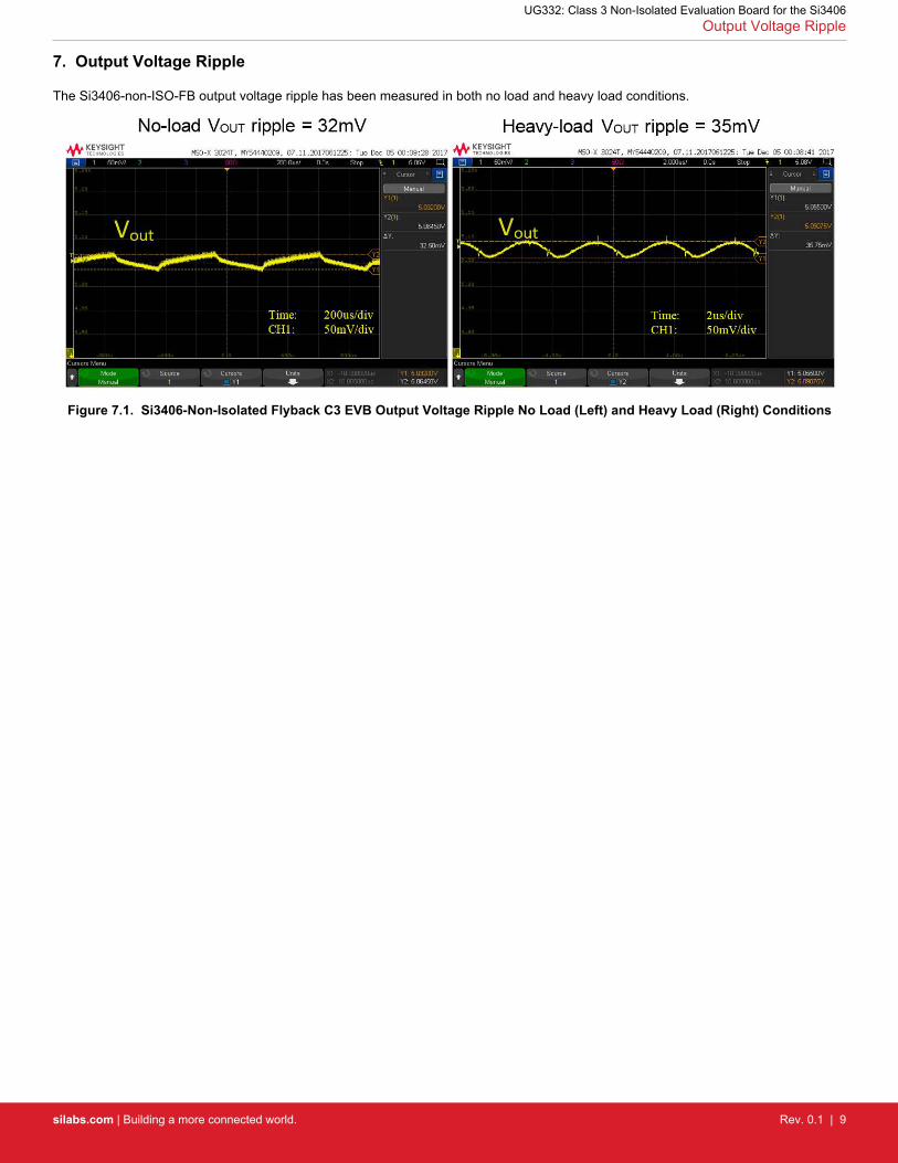
7. Output Voltage Ripple
The Si3406-non-ISO-FB output voltage ripple has been measured in both no load and heavy load conditions.
Figure 7.1. Si3406-Non-Isolated Flyback C3 EVB Output Voltage Ripple No Load (Left) and Heavy Load (Right) Conditions
UG332: Class 3 Non-Isolated Evaluation Board for the Si3406Output Voltage Ripple
silabs.com | Building a more connected world. Rev. 0.1 | 9
8. Soft Start Protection
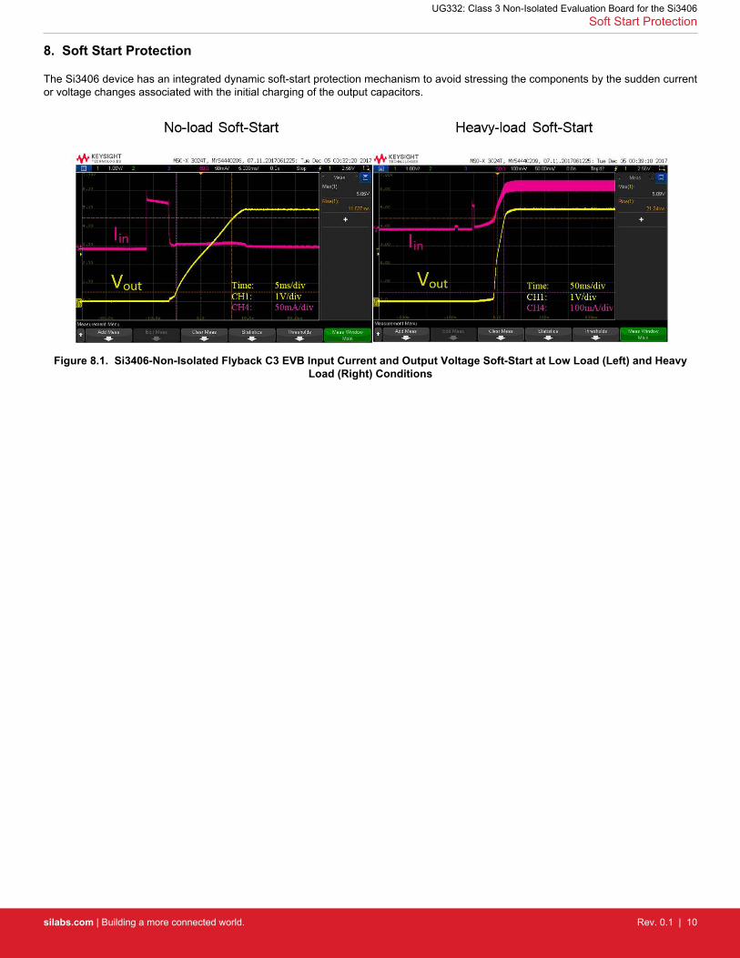
The Si3406 device has an integrated dynamic soft-start protection mechanism to avoid stressing the components by the sudden currentor voltage changes associated with the initial charging of the output capacitors.
Figure 8.1. Si3406-Non-Isolated Flyback C3 EVB Input Current and Output Voltage Soft-Start at Low Load (Left) and HeavyLoad (Right) Conditions
UG332: Class 3 Non-Isolated Evaluation Board for the Si3406Soft Start Protection
silabs.com | Building a more connected world. Rev. 0.1 | 10

9. Output Short Protection
The Si3406 device has an integrated output short protection mechanism, which protects the IC itself and the surrounding external com-ponents from overheating in the case of electrical short on the output.
Figure 9.1. Si3406-Non-Isolated Flyback C3 EVB Output Voltage and Input Current when Output is Shorted
UG332: Class 3 Non-Isolated Evaluation Board for the Si3406Output Short Protection
silabs.com | Building a more connected world. Rev. 0.1 | 11

10. Pulse Skipping at No-Load Condition
The Si3406 device has an integrated pulse skipping mechanism to ensure ultra-low power consumption at no load condition.
Figure 10.1. Si3406 Pulse Skipping at No-load Condition: SWO Waveform
UG332: Class 3 Non-Isolated Evaluation Board for the Si3406Pulse Skipping at No-Load Condition
silabs.com | Building a more connected world. Rev. 0.1 | 12

11. Adjustable EVB Current Limit
For additional safety, the Si3406 has an adjustable EVB current limit feature. The EVB current limit through the ISNS pin measures thevoltage on RSENSE. When VRSENSE = -270 mV (referenced to Vss), the current limit circuit restarts the circuit to protect the application.
The EVB current limit for this Class 3 application can be calculated with the following formula:RSENSE = 0.62Ω
ILIMIT = 270mV0.62Ω = 435mA
Equation 1. EVB Current Limit
UG332: Class 3 Non-Isolated Evaluation Board for the Si3406Adjustable EVB Current Limit
silabs.com | Building a more connected world. Rev. 0.1 | 13

12. Tunable Switching Frequency
The switching frequency of the oscillator is selected by choosing an external resistor (RFREQ) connected between the RFREQ andVPOS pins. The following figure will aid in choosing the RFREQ value to achieve the desired switching frequency.
Figure 12.1. Switching Frequency vs RFREQ
The selected switching frequency for this application is 220 kHz, which is achieved by setting the RFREQ resistor to 88.7 kΩ.
UG332: Class 3 Non-Isolated Evaluation Board for the Si3406Tunable Switching Frequency
silabs.com | Building a more connected world. Rev. 0.1 | 14

13. Synchronous Rectification
The Si3406 device has synchronous gate driver (SYNCL) to drive the rectifier MOSFET. At low-load the converter works in discontinu-ous current mode (DCM); at heavy load, the converter runs in continuous current mode (CCM). At low-load the SWO voltage waveformhas a ringing waveform, which is typical for a DCM operation.
Figure 13.1. SWO and SYNCL Voltage Waveforms at Discontinuous Current Mode (DCM) (Left) and in Continuous CurrentMode (CCM) (Right)
The device operates in non-synchronous mode at light load (IIN < 25 mA). As the input current increases, Si3406 automatically changesits switching operation from "Non-Synchronous" to "Synchronous". The dynamic operation adjustment maximizes overall power efficien-cy.
UG332: Class 3 Non-Isolated Evaluation Board for the Si3406Synchronous Rectification
silabs.com | Building a more connected world. Rev. 0.1 | 15
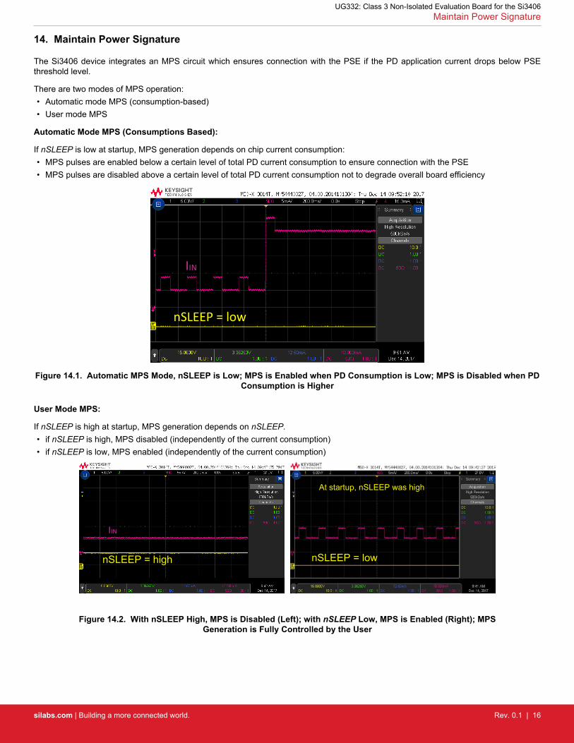
14. Maintain Power Signature
The Si3406 device integrates an MPS circuit which ensures connection with the PSE if the PD application current drops below PSEthreshold level.
There are two modes of MPS operation:• Automatic mode MPS (consumption-based)• User mode MPS
Automatic Mode MPS (Consumptions Based):
If nSLEEP is low at startup, MPS generation depends on chip current consumption:• MPS pulses are enabled below a certain level of total PD current consumption to ensure connection with the PSE• MPS pulses are disabled above a certain level of total PD current consumption not to degrade overall board efficiency
nSLEEP = low
IIN
Figure 14.1. Automatic MPS Mode, nSLEEP is Low; MPS is Enabled when PD Consumption is Low; MPS is Disabled when PDConsumption is Higher
User Mode MPS:
If nSLEEP is high at startup, MPS generation depends on nSLEEP.• if nSLEEP is high, MPS disabled (independently of the current consumption)• if nSLEEP is low, MPS enabled (independently of the current consumption)
nSLEEP = high
IIN
nSLEEP = low
At startup, nSLEEP was high
Figure 14.2. With nSLEEP High, MPS is Disabled (Left); with nSLEEP Low, MPS is Enabled (Right); MPSGeneration is Fully Controlled by the User
UG332: Class 3 Non-Isolated Evaluation Board for the Si3406Maintain Power Signature
silabs.com | Building a more connected world. Rev. 0.1 | 16
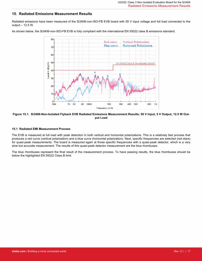
15. Radiated Emissions Measurement Results
Radiated emissions have been measured of the Si3406-non-ISO-FB EVB board with 50 V input voltage and full load connected to theoutput – 12.5 W.
As shown below, the Si3406-non-ISO-FB EVB is fully compliant with the international EN 55022 class B emissions standard.
Figure 15.1. Si3406-Non-Isolated Flyback EVB Radiated Emissions Measurement Results; 50 V Input, 5 V Output, 12.5 W Out-put Load
15.1 Radiated EMI Measurement Process
The EVB is measured at full load with peak detection in both vertical and horizontal polarizations. This is a relatively fast process thatproduces a red curve (vertical polarization) and a blue curve (horizontal polarization). Next, specific frequencies are selected (red stars)for quasi-peak measurements. The board is measured again at those specific frequencies with a quasi-peak detector, which is a veryslow but accurate measurement. The results of this quasi-peak detector measurement are the blue rhombuses.
The blue rhombuses represent the final result of the measurement process. To have passing results, the blue rhombuses should bebelow the highlighted EN 55022 Class B limit.
UG332: Class 3 Non-Isolated Evaluation Board for the Si3406Radiated Emissions Measurement Results
silabs.com | Building a more connected world. Rev. 0.1 | 17
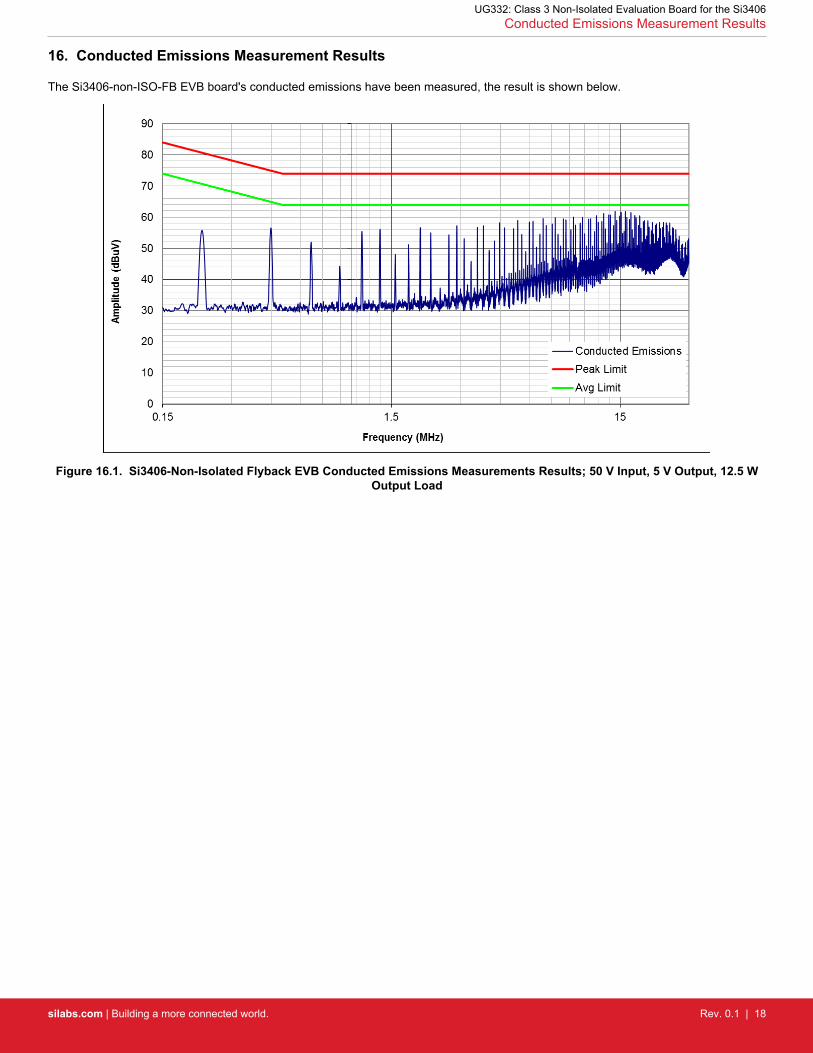
16. Conducted Emissions Measurement Results
The Si3406-non-ISO-FB EVB board's conducted emissions have been measured, the result is shown below.
Figure 16.1. Si3406-Non-Isolated Flyback EVB Conducted Emissions Measurements Results; 50 V Input, 5 V Output, 12.5 WOutput Load
UG332: Class 3 Non-Isolated Evaluation Board for the Si3406Conducted Emissions Measurement Results
silabs.com | Building a more connected world. Rev. 0.1 | 18

17. Board Layout
Figure 17.1. Top Silkscreen
Figure 17.2. Top Layer
UG332: Class 3 Non-Isolated Evaluation Board for the Si3406Board Layout
silabs.com | Building a more connected world. Rev. 0.1 | 19
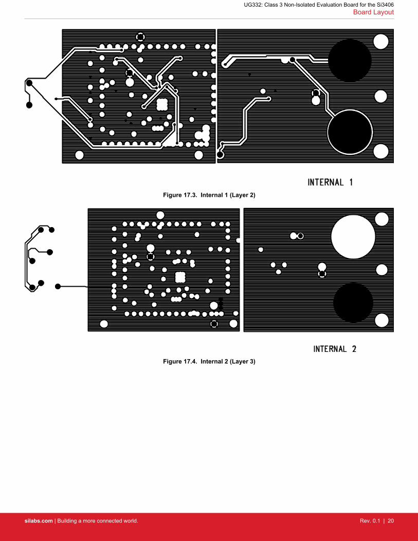
Figure 17.3. Internal 1 (Layer 2)
Figure 17.4. Internal 2 (Layer 3)
UG332: Class 3 Non-Isolated Evaluation Board for the Si3406Board Layout
silabs.com | Building a more connected world. Rev. 0.1 | 20

Figure 17.5. Bottom Layer
UG332: Class 3 Non-Isolated Evaluation Board for the Si3406Board Layout
silabs.com | Building a more connected world. Rev. 0.1 | 21
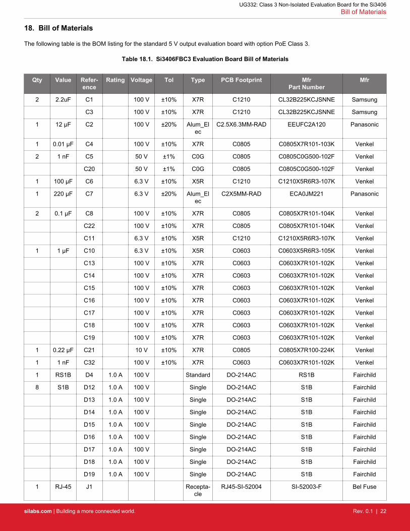
18. Bill of Materials
The following table is the BOM listing for the standard 5 V output evaluation board with option PoE Class 3.
Table 18.1. Si3406FBC3 Evaluation Board Bill of Materials
Qty Value Refer-ence
Rating Voltage Tol Type PCB Footprint MfrPart Number
Mfr
2 2.2uF C1 100 V ±10% X7R C1210 CL32B225KCJSNNE Samsung
C3 100 V ±10% X7R C1210 CL32B225KCJSNNE Samsung
1 12 µF C2 100 V ±20% Alum_Elec
C2.5X6.3MM-RAD EEUFC2A120 Panasonic
1 0.01 µF C4 100 V ±10% X7R C0805 C0805X7R101-103K Venkel
2 1 nF C5 50 V ±1% C0G C0805 C0805C0G500-102F Venkel
C20 50 V ±1% C0G C0805 C0805C0G500-102F Venkel
1 100 µF C6 6.3 V ±10% X5R C1210 C1210X5R6R3-107K Venkel
1 220 µF C7 6.3 V ±20% Alum_Elec
C2X5MM-RAD ECA0JM221 Panasonic
2 0.1 µF C8 100 V ±10% X7R C0805 C0805X7R101-104K Venkel
C22 100 V ±10% X7R C0805 C0805X7R101-104K Venkel
C11 6.3 V ±10% X5R C1210 C1210X5R6R3-107K Venkel
1 1 µF C10 6.3 V ±10% X5R C0603 C0603X5R6R3-105K Venkel
C13 100 V ±10% X7R C0603 C0603X7R101-102K Venkel
C14 100 V ±10% X7R C0603 C0603X7R101-102K Venkel
C15 100 V ±10% X7R C0603 C0603X7R101-102K Venkel
C16 100 V ±10% X7R C0603 C0603X7R101-102K Venkel
C17 100 V ±10% X7R C0603 C0603X7R101-102K Venkel
C18 100 V ±10% X7R C0603 C0603X7R101-102K Venkel
C19 100 V ±10% X7R C0603 C0603X7R101-102K Venkel
1 0.22 µF C21 10 V ±10% X7R C0805 C0805X7R100-224K Venkel
1 1 nF C32 100 V ±10% X7R C0603 C0603X7R101-102K Venkel
1 RS1B D4 1.0 A 100 V Standard DO-214AC RS1B Fairchild
8 S1B D12 1.0 A 100 V Single DO-214AC S1B Fairchild
D13 1.0 A 100 V Single DO-214AC S1B Fairchild
D14 1.0 A 100 V Single DO-214AC S1B Fairchild
D15 1.0 A 100 V Single DO-214AC S1B Fairchild
D16 1.0 A 100 V Single DO-214AC S1B Fairchild
D17 1.0 A 100 V Single DO-214AC S1B Fairchild
D18 1.0 A 100 V Single DO-214AC S1B Fairchild
D19 1.0 A 100 V Single DO-214AC S1B Fairchild
1 RJ-45 J1 Recepta-cle
RJ45-SI-52004 SI-52003-F Bel Fuse
UG332: Class 3 Non-Isolated Evaluation Board for the Si3406Bill of Materials
silabs.com | Building a more connected world. Rev. 0.1 | 22

Qty Value Refer-ence
Rating Voltage Tol Type PCB Footprint MfrPart Number
Mfr
2 BND_POST
J11 15 A BANANA BANANA-JACK 101 ABBATRONHH SMITH
J12 15 A BANANA BANANA-JACK 101 ABBATRONHH SMITH
4 330 Ω L1 1500mA
SMT L0805 BLM21PG331SN1 Murata
L2 1500mA
SMT L0805 BLM21PG331SN1 Murata
L4 1500mA
SMT L0805 BLM21PG331SN1 Murata
L5 1500mA
SMT L0805 BLM21PG331SN1 Murata
1 1 µH L3 2.9 A ±20% Shielded IND-6.6X4.45MM DO1608C-102ML_ Coilcraft
1 FDMA8051L
Q1 10 A 40 V N-CHNL DFN6N2X2P0.65E1.0X1.05
FDMA8051L Fairchild
2 330 Ω R1 1/10 W ±1% Thick-Film
R0805 CR0805-10W-3300F Venkel
R2 1/10 W ±1% Thick-Film
R0805 CR0805-10W-3300F Venkel
1 27 kΩ R4 1/8 W ±1% Thick-Film
R0805 RC0805FR-0727KL Yageo
1 6.8 Ω R5 1/8 W ±1% Thick-Film
R0805 RC0805FR-076R8L Yageo
1 88.7 kΩ R8 1/8 W ±1% Thick-Film
R0805 CRCW080588K7FKEA Vishay
1 48.7 Ω R10 1/8 W ±1% Thick-Film
R0805 CRCW080548R7FKTA vishay
1 24.3 kΩ R11 1/8 W ±1% Thick-Film
R0805 CRCW080524K3FKEA vishay
1 0.62 Ω R13 1/8 W ±1% Thick-Film
R0805 RL0805FR-070R62L Yageo
1 9.1 kΩ R14 1/8 W ±1% Thick-Film
R0805 RC0805FR-079K1L Yageo
1 3.24 kΩ R15 1/8 W ±1% Thick-Film
R0805 CRCW08053K24FKEA Vishay
1 47 kΩ R20 1/10 W ±5% Thick-Film
R0805 CR0805-10W-473J Venkel
1 0 R21 2 A Thick-Film
R0805 CR0805-10W-000 Venkel
1 FA2924 T1 XFMR-FA2924 FA2924-AL Coilcraft
1 Si3406 U1 120 V PD QFN20N5X5P0.8 Si3406 Silabs
Not Installed Components
2 100 µF C9 6.3 V ±10% X5R C1210 C1210X5R6R3-107K Venkel
8 1 nF C12 100 V ±10% X7R C0603 C0603X7R101-102K Venkel
UG332: Class 3 Non-Isolated Evaluation Board for the Si3406Bill of Materials
silabs.com | Building a more connected world. Rev. 0.1 | 23

1 330 pF C31 100 V ±20% X7R C0805 C0805X7R101-331M Venkel
1 1N4148W
D5 300 mA 100 V Single SOD-123 1N4148W-7-F Diodes Inc.
UG332: Class 3 Non-Isolated Evaluation Board for the Si3406Bill of Materials
silabs.com | Building a more connected world. Rev. 0.1 | 24
19. Appendix—Si3406-Non-ISO-FB Design and Layout Checklist
Although the EVB design is pre-configured as a Class 3 PD with 5 V output, the schematics and layouts can easily be adapted to meeta wide variety of common output voltages and power levels.
The complete EVB design databases for the standard 5 V/Class 3 configuration are located at www.silabs.com/PoE link. Silicon Labsstrongly recommends using these EVB schematics and layout files as a starting point to ensure robust performance and avoid commonmistakes in the schematic capture and PCB layout processes.
Below is a recommended design checklist that can assist in trouble-free development of robust PD designs.
Refer also to the Si3406-non-ISO-FB data sheet and AN1130 when using the following checklist.1. Design Planning checklist:
a. Determine if your design requires an isolated or non-isolated topology. For more information, see AN1130.b. Silicon Labs strongly recommends using the EVB schematics and layout files as a starting point as you begin integrating the
Si3406-non-ISO-FB into your system design process.c. Determine your load’s power requirements (i.e., VOUT and IOUT consumed by the PD, including the typical expected transi-
ent surge conditions). In general, to achieve the highest overall efficiency performance of the Si3406-non-isolated Flyback,choose the highest output voltage option used in your PD and then post regulate to the lower supply rails, if necessary.
d. Based on your required PD power level, select the appropriate class resistor RCLASS value by referring to AN1130.2. General Design checklist:
a. ESD caps (C12–C19 in Figure 2.3 Si3406-Non-Isolated Flyback EVB Schematic: 5 V, Class 3 PD on page 4) are stronglyrecommended for designs where system-level ESD (IEC6100-4-2) must provide >15 kV tolerance.
b. If your design uses an AUX supply, be sure to include a 3 Ω surge limiting resistor in series with the AUX supply for hot inser-tion. Refer to AN1130 when AUX supply is 48 V.
3. Layout Guidelines:a. Make sure VNEG pin of the Si3406 is connected to the backside of the QFN package with an adequate thermal plane, as
noted in the data sheet and AN1130.b. Keep the trace length from SWO to VSS as short as possible. Make all of the power (high current) traces as short, direct, and
thick as possible. It is a good practice on a standard PCB board to make the traces an absolute minimum of 15 mils (0.381mm) per ampere.
c. Usually, one standard via handles 200 mA of current. If the trace needs to conduct a significant amount of current from oneplane to the other, use multiple vias.
d. Keep the circular area of the loop from the Switcher FET output to the inductor or transformer and returning from the input filtercapacitors (C1–C3) to VSS as small a diameter as possible. Also, minimize the circular area of the loop from the output of theinductor or transformer to the Schottky diode and returning through the first stage output filter capacitor back to the inductor ortransformer as small as possible. If possible, keep the direction of current flow in these two loops the same.
e. Keep the high power traces as short as possible.f. Keep the feedback and loop stability components as far from the transformer/inductor and noisy power traces as possible.g. If the outputs have a ground plane or positive output plane, do not connect the high current carrying components and the filter
capacitors through the plane. Connect them together, and then connect to the plane at a single point.
To help ensure first-pass success, contact our customer support by submitting a help ticket and uploading your schematics and layoutfiles for review.
UG332: Class 3 Non-Isolated Evaluation Board for the Si3406Appendix—Si3406-Non-ISO-FB Design and Layout Checklist
silabs.com | Building a more connected world. Rev. 0.1 | 25

http://www.silabs.com
Silicon Laboratories Inc.400 West Cesar ChavezAustin, TX 78701USA
Smart. Connected. Energy-Friendly.
Productswww.silabs.com/products
Qualitywww.silabs.com/quality
Support and Communitycommunity.silabs.com
DisclaimerSilicon Labs intends to provide customers with the latest, accurate, and in-depth documentation of all peripherals and modules available for system and software implementers using or intending to use the Silicon Labs products. Characterization data, available modules and peripherals, memory sizes and memory addresses refer to each specific device, and "Typical" parameters provided can and do vary in different applications. Application examples described herein are for illustrative purposes only. Silicon Labs reserves the right to make changes without further notice and limitation to product information, specifications, and descriptions herein, and does not give warranties as to the accuracy or completeness of the included information. Silicon Labs shall have no liability for the consequences of use of the information supplied herein. This document does not imply or express copyright licenses granted hereunder to design or fabricate any integrated circuits. The products are not designed or authorized to be used within any Life Support System without the specific written consent of Silicon Labs. A "Life Support System" is any product or system intended to support or sustain life and/or health, which, if it fails, can be reasonably expected to result in significant personal injury or death. Silicon Labs products are not designed or authorized for military applications. Silicon Labs products shall under no circumstances be used in weapons of mass destruction including (but not limited to) nuclear, biological or chemical weapons, or missiles capable of delivering such weapons.
Trademark InformationSilicon Laboratories Inc.® , Silicon Laboratories®, Silicon Labs®, SiLabs® and the Silicon Labs logo®, Bluegiga®, Bluegiga Logo®, Clockbuilder®, CMEMS®, DSPLL®, EFM®, EFM32®, EFR, Ember®, Energy Micro, Energy Micro logo and combinations thereof, "the world’s most energy friendly microcontrollers", Ember®, EZLink®, EZRadio®, EZRadioPRO®, Gecko®, ISOmodem®, Micrium, Precision32®, ProSLIC®, Simplicity Studio®, SiPHY®, Telegesis, the Telegesis Logo®, USBXpress®, Zentri and others are trademarks or registered trademarks of Silicon Labs. ARM, CORTEX, Cortex-M3 and THUMB are trademarks or registered trademarks of ARM Holdings. Keil is a registered trademark of ARM Limited. All other products or brand names mentioned herein are trademarks of their respective holders.