ug dsp builder
TRANSCRIPT

101 Innovation DriveSan Jose, CA 95134www.altera.com
DSP BuilderUser Guide
Software Version: 9.0Document Date: March 2009

Copyright © 2009 Altera Corporation. All rights reserved. Altera, The Programmable Solutions Company, the stylized Altera logo, specific device designations, and all otherwords and logos that are identified as trademarks and/or service marks are, unless noted otherwise, the trademarks and service marks of Altera Corporation in the U.S. and othercountries. All other product or service names are the property of their respective holders. Altera products are protected under numerous U.S. and foreign patents and pending ap-plications, maskwork rights, and copyrights. Altera warrants performance of its semiconductor products to current specifications in accordance with Altera's standard warranty,but reserves the right to make changes to any products and services at any time without notice. Altera assumes no responsibility or liability arising out of the application or use ofany information, product, or service described herein except as expressly agreed to in writing by Altera Corporation. Altera customers are advised to obtain the latest version ofdevice specifications before relying on any published information and before placing orders for products or services.
UG-DSPBUILDER-9.0

© March 2009 Altera Corporation DSP Builder User Guide
Contents
Chapter 1. About DSP BuilderNew Features . . . . . . . . . . . . . . . . . . . . . . . . . . . . . . . . . . . . . . . . . . . . . . . . . . . . . . . . . . . . . . . . . . . . . . . . . . . 1–1Release Information . . . . . . . . . . . . . . . . . . . . . . . . . . . . . . . . . . . . . . . . . . . . . . . . . . . . . . . . . . . . . . . . . . . . . 1–1Device Family Support . . . . . . . . . . . . . . . . . . . . . . . . . . . . . . . . . . . . . . . . . . . . . . . . . . . . . . . . . . . . . . . . . . . 1–1
Memory Options . . . . . . . . . . . . . . . . . . . . . . . . . . . . . . . . . . . . . . . . . . . . . . . . . . . . . . . . . . . . . . . . . . . . . . 1–1Features . . . . . . . . . . . . . . . . . . . . . . . . . . . . . . . . . . . . . . . . . . . . . . . . . . . . . . . . . . . . . . . . . . . . . . . . . . . . . . . . 1–2Installing DSP Builder . . . . . . . . . . . . . . . . . . . . . . . . . . . . . . . . . . . . . . . . . . . . . . . . . . . . . . . . . . . . . . . . . . . 1–3General Description . . . . . . . . . . . . . . . . . . . . . . . . . . . . . . . . . . . . . . . . . . . . . . . . . . . . . . . . . . . . . . . . . . . . . 1–3
High-Speed DSP with Programmable Logic . . . . . . . . . . . . . . . . . . . . . . . . . . . . . . . . . . . . . . . . . . . . . . 1–3Design Flow . . . . . . . . . . . . . . . . . . . . . . . . . . . . . . . . . . . . . . . . . . . . . . . . . . . . . . . . . . . . . . . . . . . . . . . . . . . . 1–4
Interoperability with the Advanced Blockset . . . . . . . . . . . . . . . . . . . . . . . . . . . . . . . . . . . . . . . . . . . . . . 1–6
Chapter 2. Getting Started TutorialIntroduction . . . . . . . . . . . . . . . . . . . . . . . . . . . . . . . . . . . . . . . . . . . . . . . . . . . . . . . . . . . . . . . . . . . . . . . . . . . . 2–1Creating the Amplitude Modulation Model . . . . . . . . . . . . . . . . . . . . . . . . . . . . . . . . . . . . . . . . . . . . . . . . . 2–1
Create a New Model . . . . . . . . . . . . . . . . . . . . . . . . . . . . . . . . . . . . . . . . . . . . . . . . . . . . . . . . . . . . . . . . . . 2–1Add the Sine Wave Block . . . . . . . . . . . . . . . . . . . . . . . . . . . . . . . . . . . . . . . . . . . . . . . . . . . . . . . . . . . . . . 2–2Add the SinIn Block . . . . . . . . . . . . . . . . . . . . . . . . . . . . . . . . . . . . . . . . . . . . . . . . . . . . . . . . . . . . . . . . . . . 2–3Add the Delay Block . . . . . . . . . . . . . . . . . . . . . . . . . . . . . . . . . . . . . . . . . . . . . . . . . . . . . . . . . . . . . . . . . . 2–5Add the SinDelay and SinIn2 Blocks . . . . . . . . . . . . . . . . . . . . . . . . . . . . . . . . . . . . . . . . . . . . . . . . . . . . . 2–6Add the Mux Block . . . . . . . . . . . . . . . . . . . . . . . . . . . . . . . . . . . . . . . . . . . . . . . . . . . . . . . . . . . . . . . . . . . 2–7Add the Random Bitstream Block . . . . . . . . . . . . . . . . . . . . . . . . . . . . . . . . . . . . . . . . . . . . . . . . . . . . . . . 2–8Add the Noise Block . . . . . . . . . . . . . . . . . . . . . . . . . . . . . . . . . . . . . . . . . . . . . . . . . . . . . . . . . . . . . . . . . . 2–9Add the Bus Builder Block . . . . . . . . . . . . . . . . . . . . . . . . . . . . . . . . . . . . . . . . . . . . . . . . . . . . . . . . . . . . 2–10Add the GND Block . . . . . . . . . . . . . . . . . . . . . . . . . . . . . . . . . . . . . . . . . . . . . . . . . . . . . . . . . . . . . . . . . . 2–11Add the Product Block . . . . . . . . . . . . . . . . . . . . . . . . . . . . . . . . . . . . . . . . . . . . . . . . . . . . . . . . . . . . . . . . 2–11Add the StreamMod and StreamBit Blocks . . . . . . . . . . . . . . . . . . . . . . . . . . . . . . . . . . . . . . . . . . . . . . 2–12Add the Scope Block . . . . . . . . . . . . . . . . . . . . . . . . . . . . . . . . . . . . . . . . . . . . . . . . . . . . . . . . . . . . . . . . . 2–14Add a Clock Block . . . . . . . . . . . . . . . . . . . . . . . . . . . . . . . . . . . . . . . . . . . . . . . . . . . . . . . . . . . . . . . . . . . 2–15
Simulating the Model in Simulink . . . . . . . . . . . . . . . . . . . . . . . . . . . . . . . . . . . . . . . . . . . . . . . . . . . . . . . . 2–16Compiling the Design . . . . . . . . . . . . . . . . . . . . . . . . . . . . . . . . . . . . . . . . . . . . . . . . . . . . . . . . . . . . . . . . . . . 2–18Performing RTL Simulation . . . . . . . . . . . . . . . . . . . . . . . . . . . . . . . . . . . . . . . . . . . . . . . . . . . . . . . . . . . . . . 2–19Adding the Design to a Quartus II Project . . . . . . . . . . . . . . . . . . . . . . . . . . . . . . . . . . . . . . . . . . . . . . . . . 2–21
Creating a Quartus II Project . . . . . . . . . . . . . . . . . . . . . . . . . . . . . . . . . . . . . . . . . . . . . . . . . . . . . . . . . . 2–21Add the DSP Builder Design to the Project . . . . . . . . . . . . . . . . . . . . . . . . . . . . . . . . . . . . . . . . . . . . . . 2–22
Chapter 3. Design Rules and ProceduresDSP Builder Naming Conventions . . . . . . . . . . . . . . . . . . . . . . . . . . . . . . . . . . . . . . . . . . . . . . . . . . . . . . . . . 3–1Using a MATLAB Variable . . . . . . . . . . . . . . . . . . . . . . . . . . . . . . . . . . . . . . . . . . . . . . . . . . . . . . . . . . . . . . . 3–1Fixed-Point Notation . . . . . . . . . . . . . . . . . . . . . . . . . . . . . . . . . . . . . . . . . . . . . . . . . . . . . . . . . . . . . . . . . . . . . 3–2
Binary Point Location in Signed Binary Fractional Format . . . . . . . . . . . . . . . . . . . . . . . . . . . . . . . . . . 3–3Bit Width Design Rule . . . . . . . . . . . . . . . . . . . . . . . . . . . . . . . . . . . . . . . . . . . . . . . . . . . . . . . . . . . . . . . . . . . 3–4
Data Width Propagation . . . . . . . . . . . . . . . . . . . . . . . . . . . . . . . . . . . . . . . . . . . . . . . . . . . . . . . . . . . . . . . 3–4Tapped Delay Line . . . . . . . . . . . . . . . . . . . . . . . . . . . . . . . . . . . . . . . . . . . . . . . . . . . . . . . . . . . . . . . . . 3–5Arithmetic Operation . . . . . . . . . . . . . . . . . . . . . . . . . . . . . . . . . . . . . . . . . . . . . . . . . . . . . . . . . . . . . . . 3–5
Frequency Design Rules . . . . . . . . . . . . . . . . . . . . . . . . . . . . . . . . . . . . . . . . . . . . . . . . . . . . . . . . . . . . . . . . . . 3–7Single Clock Domain . . . . . . . . . . . . . . . . . . . . . . . . . . . . . . . . . . . . . . . . . . . . . . . . . . . . . . . . . . . . . . . . . . 3–7Multiple Clock Domains . . . . . . . . . . . . . . . . . . . . . . . . . . . . . . . . . . . . . . . . . . . . . . . . . . . . . . . . . . . . . . . 3–8

2 Contents
DSP Builder User Guide © March 2009 Altera Corporation
Using Clock and Clock_Derived Blocks . . . . . . . . . . . . . . . . . . . . . . . . . . . . . . . . . . . . . . . . . . . . . . . . . 3–10Clock Assignment . . . . . . . . . . . . . . . . . . . . . . . . . . . . . . . . . . . . . . . . . . . . . . . . . . . . . . . . . . . . . . . . . . . . 3–10Using the PLL Block . . . . . . . . . . . . . . . . . . . . . . . . . . . . . . . . . . . . . . . . . . . . . . . . . . . . . . . . . . . . . . . . . . 3–13
Using Advanced PLL Features . . . . . . . . . . . . . . . . . . . . . . . . . . . . . . . . . . . . . . . . . . . . . . . . . . . . . . 3–15Timing Semantics Between Simulink and HDL Simulation . . . . . . . . . . . . . . . . . . . . . . . . . . . . . . . . . . . 3–15
Simulink Simulation Model . . . . . . . . . . . . . . . . . . . . . . . . . . . . . . . . . . . . . . . . . . . . . . . . . . . . . . . . . . . 3–15HDL Simulation Models . . . . . . . . . . . . . . . . . . . . . . . . . . . . . . . . . . . . . . . . . . . . . . . . . . . . . . . . . . . . . . 3–15Startup & Initial Conditions . . . . . . . . . . . . . . . . . . . . . . . . . . . . . . . . . . . . . . . . . . . . . . . . . . . . . . . . . . . 3–16DSP Builder Global Reset Circuitry . . . . . . . . . . . . . . . . . . . . . . . . . . . . . . . . . . . . . . . . . . . . . . . . . . . . . 3–16Reference Timing Diagram . . . . . . . . . . . . . . . . . . . . . . . . . . . . . . . . . . . . . . . . . . . . . . . . . . . . . . . . . . . . 3–17
Signal Compiler and TestBench Blocks . . . . . . . . . . . . . . . . . . . . . . . . . . . . . . . . . . . . . . . . . . . . . . . . . . . . 3–18Design Flows for Synthesis, Compilation and Simulation . . . . . . . . . . . . . . . . . . . . . . . . . . . . . . . . . . 3–18
Hierarchical Design . . . . . . . . . . . . . . . . . . . . . . . . . . . . . . . . . . . . . . . . . . . . . . . . . . . . . . . . . . . . . . . . . . . . . 3–19Goto and From Block Support . . . . . . . . . . . . . . . . . . . . . . . . . . . . . . . . . . . . . . . . . . . . . . . . . . . . . . . . . . . . 3–20Black Boxing and HDL Import . . . . . . . . . . . . . . . . . . . . . . . . . . . . . . . . . . . . . . . . . . . . . . . . . . . . . . . . . . . 3–21Using a MATLAB Array or HEX File to Initialize a Block . . . . . . . . . . . . . . . . . . . . . . . . . . . . . . . . . . . . 3–21Comparison Utility . . . . . . . . . . . . . . . . . . . . . . . . . . . . . . . . . . . . . . . . . . . . . . . . . . . . . . . . . . . . . . . . . . . . . 3–21Adding Comments to Blocks . . . . . . . . . . . . . . . . . . . . . . . . . . . . . . . . . . . . . . . . . . . . . . . . . . . . . . . . . . . . . 3–21Adding Quartus II Constraints . . . . . . . . . . . . . . . . . . . . . . . . . . . . . . . . . . . . . . . . . . . . . . . . . . . . . . . . . . . 3–22Displaying Port Data Types . . . . . . . . . . . . . . . . . . . . . . . . . . . . . . . . . . . . . . . . . . . . . . . . . . . . . . . . . . . . . . 3–23Displaying the Pipeline Depth . . . . . . . . . . . . . . . . . . . . . . . . . . . . . . . . . . . . . . . . . . . . . . . . . . . . . . . . . . . 3–23Updating HDL Import Blocks . . . . . . . . . . . . . . . . . . . . . . . . . . . . . . . . . . . . . . . . . . . . . . . . . . . . . . . . . . . . 3–23Analyzing the Hardware Resource Usage . . . . . . . . . . . . . . . . . . . . . . . . . . . . . . . . . . . . . . . . . . . . . . . . . . 3–24Loading Additional ModelSim Commands . . . . . . . . . . . . . . . . . . . . . . . . . . . . . . . . . . . . . . . . . . . . . . . . 3–26Making Quartus II Assignments to Block Entity Names . . . . . . . . . . . . . . . . . . . . . . . . . . . . . . . . . . . . . 3–26
Chapter 4. Using MegaCore FunctionsIntroduction . . . . . . . . . . . . . . . . . . . . . . . . . . . . . . . . . . . . . . . . . . . . . . . . . . . . . . . . . . . . . . . . . . . . . . . . . . . . 4–1Installing MegaCore Functions . . . . . . . . . . . . . . . . . . . . . . . . . . . . . . . . . . . . . . . . . . . . . . . . . . . . . . . . . . . . 4–1Updating MegaCore Function Variation Blocks . . . . . . . . . . . . . . . . . . . . . . . . . . . . . . . . . . . . . . . . . . . . . . 4–2Using Previous Versions of MegaCore Functions . . . . . . . . . . . . . . . . . . . . . . . . . . . . . . . . . . . . . . . . . . . . 4–2Design Flow Using MegaCore Functions . . . . . . . . . . . . . . . . . . . . . . . . . . . . . . . . . . . . . . . . . . . . . . . . . . . 4–3
Placing the MegaCore Function in the Simulink Model . . . . . . . . . . . . . . . . . . . . . . . . . . . . . . . . . . . . . 4–3Parameterizing the MegaCore Function Variation . . . . . . . . . . . . . . . . . . . . . . . . . . . . . . . . . . . . . . . . . 4–3Generating the MegaCore Function Variation . . . . . . . . . . . . . . . . . . . . . . . . . . . . . . . . . . . . . . . . . . . . . 4–3Connecting the MegaCore Function Variation Block to the Design . . . . . . . . . . . . . . . . . . . . . . . . . . . 4–4Simulating the MegaCore Function Variation in the Model . . . . . . . . . . . . . . . . . . . . . . . . . . . . . . . . . 4–4
MegaCore Function Walkthrough . . . . . . . . . . . . . . . . . . . . . . . . . . . . . . . . . . . . . . . . . . . . . . . . . . . . . . . . . 4–4Creating a New Simulink Model . . . . . . . . . . . . . . . . . . . . . . . . . . . . . . . . . . . . . . . . . . . . . . . . . . . . . . . . 4–4Adding the FIR Compiler Function . . . . . . . . . . . . . . . . . . . . . . . . . . . . . . . . . . . . . . . . . . . . . . . . . . . . . . 4–4Parameterizing the FIR Compiler Function . . . . . . . . . . . . . . . . . . . . . . . . . . . . . . . . . . . . . . . . . . . . . . . 4–6Generating the FIR Compiler Function Variation . . . . . . . . . . . . . . . . . . . . . . . . . . . . . . . . . . . . . . . . . . 4–7Adding Stimulus and Scope Blocks . . . . . . . . . . . . . . . . . . . . . . . . . . . . . . . . . . . . . . . . . . . . . . . . . . . . . . 4–9Simulating the Design in Simulink . . . . . . . . . . . . . . . . . . . . . . . . . . . . . . . . . . . . . . . . . . . . . . . . . . . . . 4–11Compiling the Design . . . . . . . . . . . . . . . . . . . . . . . . . . . . . . . . . . . . . . . . . . . . . . . . . . . . . . . . . . . . . . . . 4–13Performing RTL Simulation . . . . . . . . . . . . . . . . . . . . . . . . . . . . . . . . . . . . . . . . . . . . . . . . . . . . . . . . . . . 4–14
Design Issues When Using MegaCore Functions . . . . . . . . . . . . . . . . . . . . . . . . . . . . . . . . . . . . . . . . . . . . 4–16Simulink Files Associated with a MegaCore Function . . . . . . . . . . . . . . . . . . . . . . . . . . . . . . . . . . . . . 4–16Simulating MegaCore Functions That Have a Reset Port . . . . . . . . . . . . . . . . . . . . . . . . . . . . . . . . . . 4–17Setting the Device Family for MegaCore Functions . . . . . . . . . . . . . . . . . . . . . . . . . . . . . . . . . . . . . . . 4–17
Chapter 5. Using Hardware in the Loop (HIL)Introduction . . . . . . . . . . . . . . . . . . . . . . . . . . . . . . . . . . . . . . . . . . . . . . . . . . . . . . . . . . . . . . . . . . . . . . . . . . . . 5–1
Contents 3
© March 2009 Altera Corporation DSP Builder User Guide
HIL Design Flow . . . . . . . . . . . . . . . . . . . . . . . . . . . . . . . . . . . . . . . . . . . . . . . . . . . . . . . . . . . . . . . . . . . . . . . . 5–1HIL Requirements . . . . . . . . . . . . . . . . . . . . . . . . . . . . . . . . . . . . . . . . . . . . . . . . . . . . . . . . . . . . . . . . . . . . . . . 5–2HIL Walkthrough . . . . . . . . . . . . . . . . . . . . . . . . . . . . . . . . . . . . . . . . . . . . . . . . . . . . . . . . . . . . . . . . . . . . . . . 5–3Burst & Frame Modes . . . . . . . . . . . . . . . . . . . . . . . . . . . . . . . . . . . . . . . . . . . . . . . . . . . . . . . . . . . . . . . . . . . . 5–7
Using Burst Mode . . . . . . . . . . . . . . . . . . . . . . . . . . . . . . . . . . . . . . . . . . . . . . . . . . . . . . . . . . . . . . . . . . . . . 5–8Using Frame Mode . . . . . . . . . . . . . . . . . . . . . . . . . . . . . . . . . . . . . . . . . . . . . . . . . . . . . . . . . . . . . . . . . . . . 5–9
Troubleshooting HIL Designs . . . . . . . . . . . . . . . . . . . . . . . . . . . . . . . . . . . . . . . . . . . . . . . . . . . . . . . . . . . . 5–10Failed to Load the Specified Quartus II Project . . . . . . . . . . . . . . . . . . . . . . . . . . . . . . . . . . . . . . . . . . . 5–10
Project Not Compiled Through the Quartus II Fitter . . . . . . . . . . . . . . . . . . . . . . . . . . . . . . . . . . . . 5–10Quartus II Version Mismatch . . . . . . . . . . . . . . . . . . . . . . . . . . . . . . . . . . . . . . . . . . . . . . . . . . . . . . . . 5–11Quartus II Project File is Not Up-to-Date . . . . . . . . . . . . . . . . . . . . . . . . . . . . . . . . . . . . . . . . . . . . . . 5–11
No Inputs Found From the Quartus II Project . . . . . . . . . . . . . . . . . . . . . . . . . . . . . . . . . . . . . . . . . . . . 5–11No Outputs Found From the Quartus II Project . . . . . . . . . . . . . . . . . . . . . . . . . . . . . . . . . . . . . . . . . . 5–11HIL Design Stays in Reset During Simulation . . . . . . . . . . . . . . . . . . . . . . . . . . . . . . . . . . . . . . . . . . . . 5–11HIL Compilation Appears to be Hung . . . . . . . . . . . . . . . . . . . . . . . . . . . . . . . . . . . . . . . . . . . . . . . . . . 5–11Scan JTAG Fails to Find Correct Cable or Device . . . . . . . . . . . . . . . . . . . . . . . . . . . . . . . . . . . . . . . . . 5–12
Chapter 6. Performing SignalTap II Logic AnalysisIntroduction . . . . . . . . . . . . . . . . . . . . . . . . . . . . . . . . . . . . . . . . . . . . . . . . . . . . . . . . . . . . . . . . . . . . . . . . . . . . 6–1
SignalTap II Design Flow . . . . . . . . . . . . . . . . . . . . . . . . . . . . . . . . . . . . . . . . . . . . . . . . . . . . . . . . . . . . . . 6–1SignalTap II Nodes . . . . . . . . . . . . . . . . . . . . . . . . . . . . . . . . . . . . . . . . . . . . . . . . . . . . . . . . . . . . . . . . . . . . 6–2SignalTap II Trigger Conditions . . . . . . . . . . . . . . . . . . . . . . . . . . . . . . . . . . . . . . . . . . . . . . . . . . . . . . . . . 6–2
SignalTap II Walkthrough . . . . . . . . . . . . . . . . . . . . . . . . . . . . . . . . . . . . . . . . . . . . . . . . . . . . . . . . . . . . . . . . 6–3Opening the Walkthrough Example Design . . . . . . . . . . . . . . . . . . . . . . . . . . . . . . . . . . . . . . . . . . . . . . 6–3Adding the Configuration and Connector Blocks . . . . . . . . . . . . . . . . . . . . . . . . . . . . . . . . . . . . . . . . . . 6–4Specifying the Nodes to Analyze . . . . . . . . . . . . . . . . . . . . . . . . . . . . . . . . . . . . . . . . . . . . . . . . . . . . . . . . 6–6Turning On the SignalTap II Option in Signal Compiler . . . . . . . . . . . . . . . . . . . . . . . . . . . . . . . . . . . . 6–7Specifying the Trigger Levels . . . . . . . . . . . . . . . . . . . . . . . . . . . . . . . . . . . . . . . . . . . . . . . . . . . . . . . . . . . 6–9Performing SignalTap II Analysis . . . . . . . . . . . . . . . . . . . . . . . . . . . . . . . . . . . . . . . . . . . . . . . . . . . . . . 6–10
Chapter 7. Using the Interfaces LibraryIntroduction . . . . . . . . . . . . . . . . . . . . . . . . . . . . . . . . . . . . . . . . . . . . . . . . . . . . . . . . . . . . . . . . . . . . . . . . . . . . 7–1Avalon-MM Interface . . . . . . . . . . . . . . . . . . . . . . . . . . . . . . . . . . . . . . . . . . . . . . . . . . . . . . . . . . . . . . . . . . . . 7–1Avalon-MM Interface Blocks . . . . . . . . . . . . . . . . . . . . . . . . . . . . . . . . . . . . . . . . . . . . . . . . . . . . . . . . . . . . . . 7–2
Avalon-MM Slave Block . . . . . . . . . . . . . . . . . . . . . . . . . . . . . . . . . . . . . . . . . . . . . . . . . . . . . . . . . . . . . . . 7–2Avalon-MM Master Block . . . . . . . . . . . . . . . . . . . . . . . . . . . . . . . . . . . . . . . . . . . . . . . . . . . . . . . . . . . . . . 7–4Wrapped Blocks . . . . . . . . . . . . . . . . . . . . . . . . . . . . . . . . . . . . . . . . . . . . . . . . . . . . . . . . . . . . . . . . . . . . . . 7–5
Avalon-MM Write FIFO . . . . . . . . . . . . . . . . . . . . . . . . . . . . . . . . . . . . . . . . . . . . . . . . . . . . . . . . . . . . . 7–6Avalon-MM Read FIFO . . . . . . . . . . . . . . . . . . . . . . . . . . . . . . . . . . . . . . . . . . . . . . . . . . . . . . . . . . . . . 7–8
Avalon-MM Interface Blocks Walkthrough . . . . . . . . . . . . . . . . . . . . . . . . . . . . . . . . . . . . . . . . . . . . . . . . . 7–9Adding Avalon-MM Blocks to the Example Design . . . . . . . . . . . . . . . . . . . . . . . . . . . . . . . . . . . . . . . . 7–9Verifying the Design . . . . . . . . . . . . . . . . . . . . . . . . . . . . . . . . . . . . . . . . . . . . . . . . . . . . . . . . . . . . . . . . . 7–13Running Signal Compiler . . . . . . . . . . . . . . . . . . . . . . . . . . . . . . . . . . . . . . . . . . . . . . . . . . . . . . . . . . . . . 7–14Instantiating the Design in SOPC Builder . . . . . . . . . . . . . . . . . . . . . . . . . . . . . . . . . . . . . . . . . . . . . . . . 7–15Compiling the Quartus II Project . . . . . . . . . . . . . . . . . . . . . . . . . . . . . . . . . . . . . . . . . . . . . . . . . . . . . . . 7–19Testing the DSP Builder Block from Software . . . . . . . . . . . . . . . . . . . . . . . . . . . . . . . . . . . . . . . . . . . . 7–19
Avalon-MM FIFO Walkthrough . . . . . . . . . . . . . . . . . . . . . . . . . . . . . . . . . . . . . . . . . . . . . . . . . . . . . . . . . . 7–22Opening the Walkthrough Example Design . . . . . . . . . . . . . . . . . . . . . . . . . . . . . . . . . . . . . . . . . . . . . 7–22Compiling the Design . . . . . . . . . . . . . . . . . . . . . . . . . . . . . . . . . . . . . . . . . . . . . . . . . . . . . . . . . . . . . . . . 7–22Instantiating the Design in SOPC Builder . . . . . . . . . . . . . . . . . . . . . . . . . . . . . . . . . . . . . . . . . . . . . . . . 7–24
Avalon-ST Interface . . . . . . . . . . . . . . . . . . . . . . . . . . . . . . . . . . . . . . . . . . . . . . . . . . . . . . . . . . . . . . . . . . . . 7–26Avalon-ST Packet Formats . . . . . . . . . . . . . . . . . . . . . . . . . . . . . . . . . . . . . . . . . . . . . . . . . . . . . . . . . . . . 7–27Avalon-ST Packet Format Converter . . . . . . . . . . . . . . . . . . . . . . . . . . . . . . . . . . . . . . . . . . . . . . . . . . . . 7–28

4 Contents
DSP Builder User Guide © March 2009 Altera Corporation
Chapter 8. Using Black Boxes for HDL SubsystemsIntroduction . . . . . . . . . . . . . . . . . . . . . . . . . . . . . . . . . . . . . . . . . . . . . . . . . . . . . . . . . . . . . . . . . . . . . . . . . . . . 8–1
Implicit Black Box Interface . . . . . . . . . . . . . . . . . . . . . . . . . . . . . . . . . . . . . . . . . . . . . . . . . . . . . . . . . . . . 8–1Explicit Black Box Interface . . . . . . . . . . . . . . . . . . . . . . . . . . . . . . . . . . . . . . . . . . . . . . . . . . . . . . . . . . . . . 8–1
HDL Import Walkthrough . . . . . . . . . . . . . . . . . . . . . . . . . . . . . . . . . . . . . . . . . . . . . . . . . . . . . . . . . . . . . . . . 8–1Importing Existing HDL Files . . . . . . . . . . . . . . . . . . . . . . . . . . . . . . . . . . . . . . . . . . . . . . . . . . . . . . . . . . . 8–2Simulating the HDL Import Model using Simulink . . . . . . . . . . . . . . . . . . . . . . . . . . . . . . . . . . . . . . . . 8–4
Subsystem Builder Walkthrough . . . . . . . . . . . . . . . . . . . . . . . . . . . . . . . . . . . . . . . . . . . . . . . . . . . . . . . . . . 8–6Creating a Black Box System . . . . . . . . . . . . . . . . . . . . . . . . . . . . . . . . . . . . . . . . . . . . . . . . . . . . . . . . . . . . 8–6Building the Black Box SubSystem Simulation Model . . . . . . . . . . . . . . . . . . . . . . . . . . . . . . . . . . . . . . 8–8Simulating the Subsystem Builder Model . . . . . . . . . . . . . . . . . . . . . . . . . . . . . . . . . . . . . . . . . . . . . . . 8–11Adding VHDL Dependencies to the Quartus II Project and ModelSim . . . . . . . . . . . . . . . . . . . . . . 8–12Simulate the Design in ModelSim . . . . . . . . . . . . . . . . . . . . . . . . . . . . . . . . . . . . . . . . . . . . . . . . . . . . . . 8–12
Chapter 9. Using Custom Library BlocksIntroduction . . . . . . . . . . . . . . . . . . . . . . . . . . . . . . . . . . . . . . . . . . . . . . . . . . . . . . . . . . . . . . . . . . . . . . . . . . . . 9–1Creating a Custom Library Block . . . . . . . . . . . . . . . . . . . . . . . . . . . . . . . . . . . . . . . . . . . . . . . . . . . . . . . . . . 9–1
Creating a Library Model File . . . . . . . . . . . . . . . . . . . . . . . . . . . . . . . . . . . . . . . . . . . . . . . . . . . . . . . . . . . 9–2Building the HDL Subsystem Functionality . . . . . . . . . . . . . . . . . . . . . . . . . . . . . . . . . . . . . . . . . . . . . . . 9–2Defining Parameters Using the Mask Editor . . . . . . . . . . . . . . . . . . . . . . . . . . . . . . . . . . . . . . . . . . . . . . 9–4Linking the Mask Parameters to the Block Parameters . . . . . . . . . . . . . . . . . . . . . . . . . . . . . . . . . . . . . 9–7Making the Library Block Read Only . . . . . . . . . . . . . . . . . . . . . . . . . . . . . . . . . . . . . . . . . . . . . . . . . . . . 9–8Adding the Library to the Simulink Library Browser . . . . . . . . . . . . . . . . . . . . . . . . . . . . . . . . . . . . . . . 9–8
Synchronizing a Custom Library . . . . . . . . . . . . . . . . . . . . . . . . . . . . . . . . . . . . . . . . . . . . . . . . . . . . . . . . . . 9–9
Chapter 10. Adding a Board LibraryIntroduction . . . . . . . . . . . . . . . . . . . . . . . . . . . . . . . . . . . . . . . . . . . . . . . . . . . . . . . . . . . . . . . . . . . . . . . . . . . 10–1Creating a New Board Description . . . . . . . . . . . . . . . . . . . . . . . . . . . . . . . . . . . . . . . . . . . . . . . . . . . . . . . . 10–1
Predefined Components . . . . . . . . . . . . . . . . . . . . . . . . . . . . . . . . . . . . . . . . . . . . . . . . . . . . . . . . . . . . . . 10–1Component Types . . . . . . . . . . . . . . . . . . . . . . . . . . . . . . . . . . . . . . . . . . . . . . . . . . . . . . . . . . . . . . . . . 10–1
Component Description File . . . . . . . . . . . . . . . . . . . . . . . . . . . . . . . . . . . . . . . . . . . . . . . . . . . . . . . . . . . 10–2Example Component Description File: . . . . . . . . . . . . . . . . . . . . . . . . . . . . . . . . . . . . . . . . . . . . . . . . 10–3
Board Description File . . . . . . . . . . . . . . . . . . . . . . . . . . . . . . . . . . . . . . . . . . . . . . . . . . . . . . . . . . . . . . . . 10–4Header Section . . . . . . . . . . . . . . . . . . . . . . . . . . . . . . . . . . . . . . . . . . . . . . . . . . . . . . . . . . . . . . . . . . . . 10–4Board Description Section . . . . . . . . . . . . . . . . . . . . . . . . . . . . . . . . . . . . . . . . . . . . . . . . . . . . . . . . . . 10–4
Building the Board Library . . . . . . . . . . . . . . . . . . . . . . . . . . . . . . . . . . . . . . . . . . . . . . . . . . . . . . . . . . . . . . 10–6
Chapter 11. Using the State Machine LibraryIntroduction . . . . . . . . . . . . . . . . . . . . . . . . . . . . . . . . . . . . . . . . . . . . . . . . . . . . . . . . . . . . . . . . . . . . . . . . . . . 11–1Using the State Machine Table Block . . . . . . . . . . . . . . . . . . . . . . . . . . . . . . . . . . . . . . . . . . . . . . . . . . . . . . 11–2Using the State Machine Editor Block . . . . . . . . . . . . . . . . . . . . . . . . . . . . . . . . . . . . . . . . . . . . . . . . . . . . . 11–8
Appendix A. Managing Projects and FilesIntegration with Source Control Systems . . . . . . . . . . . . . . . . . . . . . . . . . . . . . . . . . . . . . . . . . . . . . . . . . . A–1HDL Import . . . . . . . . . . . . . . . . . . . . . . . . . . . . . . . . . . . . . . . . . . . . . . . . . . . . . . . . . . . . . . . . . . . . . . . . . . . A–2MegaCore Functions . . . . . . . . . . . . . . . . . . . . . . . . . . . . . . . . . . . . . . . . . . . . . . . . . . . . . . . . . . . . . . . . . . . . A–2Memory Initialization Files . . . . . . . . . . . . . . . . . . . . . . . . . . . . . . . . . . . . . . . . . . . . . . . . . . . . . . . . . . . . . . A–2Exporting HDL . . . . . . . . . . . . . . . . . . . . . . . . . . . . . . . . . . . . . . . . . . . . . . . . . . . . . . . . . . . . . . . . . . . . . . . . A–3
Using Exported HDL . . . . . . . . . . . . . . . . . . . . . . . . . . . . . . . . . . . . . . . . . . . . . . . . . . . . . . . . . . . . . . . . . A–4Migration of DSP Builder (Standard Blockset) Files to a New Location . . . . . . . . . . . . . . . . . . . . . . . . . A–4Integration of Multiple Models in a Top-Level Quartus II Project . . . . . . . . . . . . . . . . . . . . . . . . . . . . . A–5
Design Example . . . . . . . . . . . . . . . . . . . . . . . . . . . . . . . . . . . . . . . . . . . . . . . . . . . . . . . . . . . . . . . . . . . . . A–6

Contents 5
© March 2009 Altera Corporation DSP Builder User Guide
Appendix B. TroubleshootingTroubleshooting Issues . . . . . . . . . . . . . . . . . . . . . . . . . . . . . . . . . . . . . . . . . . . . . . . . . . . . . . . . . . . . . . . . . . B–1
Loop Detected While Propagating Bit Widths . . . . . . . . . . . . . . . . . . . . . . . . . . . . . . . . . . . . . . . . . . . . B–1The MegaCore Blocks Folder Does Not Appear in Simulink . . . . . . . . . . . . . . . . . . . . . . . . . . . . . . . B–2The Synthesis Flow Does Not Run Properly . . . . . . . . . . . . . . . . . . . . . . . . . . . . . . . . . . . . . . . . . . . . . B–2
Check the Software Paths . . . . . . . . . . . . . . . . . . . . . . . . . . . . . . . . . . . . . . . . . . . . . . . . . . . . . . . . . . . B–2Change the System Path Settings . . . . . . . . . . . . . . . . . . . . . . . . . . . . . . . . . . . . . . . . . . . . . . . . . . . . B–2
DSP Development Board Troubleshooting . . . . . . . . . . . . . . . . . . . . . . . . . . . . . . . . . . . . . . . . . . . . . . B–3Signal Compiler is Unable to Checkout a Valid License . . . . . . . . . . . . . . . . . . . . . . . . . . . . . . . . . . . B–3
Verifying That Your DSP Builder Licensing Functions Properly . . . . . . . . . . . . . . . . . . . . . . . . . . B–3Verifying That the LM_LICENSE_FILE Variable Is Set Correctly . . . . . . . . . . . . . . . . . . . . . . . . . B–4Verifying the Quartus II Path . . . . . . . . . . . . . . . . . . . . . . . . . . . . . . . . . . . . . . . . . . . . . . . . . . . . . . . . B–5If You Still Cannot Get a License . . . . . . . . . . . . . . . . . . . . . . . . . . . . . . . . . . . . . . . . . . . . . . . . . . . . . B–5
SignalTap II Analysis Appears to be Hung . . . . . . . . . . . . . . . . . . . . . . . . . . . . . . . . . . . . . . . . . . . . . . B–5Error if Output Block Connected to an Altera Synthesis Block . . . . . . . . . . . . . . . . . . . . . . . . . . . . . . B–6Warning if Input/Output Blocks Conflict with clock or aclr Ports . . . . . . . . . . . . . . . . . . . . . . . . . . B–6Wiring the Asynchronous Clear Signal . . . . . . . . . . . . . . . . . . . . . . . . . . . . . . . . . . . . . . . . . . . . . . . . . . B–6Simulation Mismatch After Changing Signals or Parameters . . . . . . . . . . . . . . . . . . . . . . . . . . . . . . . B–6Error Issued when a Design Includes Pre-v7.1 Blocks . . . . . . . . . . . . . . . . . . . . . . . . . . . . . . . . . . . . . B–7Creating an Input Terminator for Debugging a Design . . . . . . . . . . . . . . . . . . . . . . . . . . . . . . . . . . . . B–7A Specified Path Cannot be Found or a File Name is Too Long . . . . . . . . . . . . . . . . . . . . . . . . . . . . . B–7Incorrect Interpretation of Number Format in Output from MegaCore Functions . . . . . . . . . . . . . B–7Simulation Mismatch For FIR Compiler MegaCore Function . . . . . . . . . . . . . . . . . . . . . . . . . . . . . . . B–7Unexpected Exception Error when Generating Blocks . . . . . . . . . . . . . . . . . . . . . . . . . . . . . . . . . . . . . B–8VHDL Entity Names Change if a Model is Modified . . . . . . . . . . . . . . . . . . . . . . . . . . . . . . . . . . . . . . B–8Algebraic Loop Causes Simulation to Fail . . . . . . . . . . . . . . . . . . . . . . . . . . . . . . . . . . . . . . . . . . . . . . . B–8Parameter Entry Problems in the DSP Block Dialog Box . . . . . . . . . . . . . . . . . . . . . . . . . . . . . . . . . . . B–9DSP Builder System Not Detected in SOPC Builder . . . . . . . . . . . . . . . . . . . . . . . . . . . . . . . . . . . . . . . B–9
Additional Information . . . . . . . . . . . . . . . . . . . . . . . . . . . . . . . . . . . . . . . . . . . . . . . . . . . . . . . . . . . . . . . . . . . Info–1Revision History . . . . . . . . . . . . . . . . . . . . . . . . . . . . . . . . . . . . . . . . . . . . . . . . . . . . . . . . . . . . . . . . . . . . . Info–1How to Contact Altera . . . . . . . . . . . . . . . . . . . . . . . . . . . . . . . . . . . . . . . . . . . . . . . . . . . . . . . . . . . . . . . . Info–2Typographic Conventions . . . . . . . . . . . . . . . . . . . . . . . . . . . . . . . . . . . . . . . . . . . . . . . . . . . . . . . . . . . . . Info–2Other Documentation . . . . . . . . . . . . . . . . . . . . . . . . . . . . . . . . . . . . . . . . . . . . . . . . . . . . . . . . . . . . . . . . . Info–3
Index

6 Contents
DSP Builder User Guide © March 2009 Altera Corporation

© March 2009 Altera Corporation DSP Builder User Guide
1. About DSP Builder
New FeaturesThis release supports the following new features:
■ Added support Linux operating systems.
f For information about installing DSP Builder on Linux, refer to DSP Builder Installation and Licensing on the Altera Literature website.
■ Added support for Arria II GX. Removed support for APEX, FLEX, and ACEX devices.
■ Removed support for the Video and Image Processing Suite MegaCore functions.
f The preferred design flow for using the Video and Image Processing Suite MegaCore functions is SOPC Builder. For information about using this flow, refer to the Video and Image Processing Suite User Guide.
■ Updated the DSP Builder integration with SOPC Builder.
Release InformationTable 1–1 provides information about this release of DSP Builder.
Device Family SupportDSP Builder supports the following Altera® device families: Stratix®, Stratix GX, Stratix II, Stratix II GX, Stratix III, Stratix IV, Arria™ GX, Arria II GX, Cyclone®, Cyclone II, and Cyclone III.
Memory OptionsA number of the blocks in the Storage library allow you to choose the required memory block type. In general, all supported memory block types are listed as options although some may not be available for all device families.
Table 1–2 on page 1–2 shows the device families which support each memory block type.
Table 1–1. DSP Builder Release Information
Item Description
Version 9.0
Release Date March 2009
Ordering Code IPT-DSPBUILDER

1–2 Chapter 1: About DSP BuilderFeatures
DSP Builder User Guide © March 2009 Altera Corporation
f For more information about each memory block type, refer to the Quartus II Help.
FeaturesDSP Builder supports the following features:
■ Links The MathWorks MATLAB (Signal Processing ToolBox and Filter Design Toolbox) and Simulink software with the Altera® Quartus® II software.
■ Automatic VHDL testbench generation and control of Quartus II compilation.
■ Provides a variety of fixed-point arithmetic and logical operators for use with the Simulink software.
■ Enables rapid prototyping using Altera DSP development boards.
■ Supports the SignalTap® II logic analyzer, an embedded signal analyzer that probes signals from the Altera device on the DSP board and imports the data into the MATLAB workspace to facilitate visual analysis.
■ HDL import of VHDL or Verilog HDL design entities and HDL defined in a Quartus II project file.
■ Hardware in the Loop (HIL) support to enable FPGA hardware accelerated co-simulation with Simulink.
■ Support for Avalon® Memory-Mapped (Avalon-MM) interfaces including user configurable blocks that you can use to build custom logic that works with the Nios® II processor and other SOPC Builder designs.
■ Support for Avalon Streaming (Avalon-ST) interfaces including an Packet Format Converter block and configurable Avalon-ST Sink and Avalon-ST Source blocks.
■ Altera DSP MegaCore® functions can be directly instanced in a DSP Builder design model.
■ Support for tabular and graphical state machine editing.
f For information about new features and errata in this release, refer to the DSP Builder Release Notes and Errata.
Table 1–2. Supported Memory Block Types
Memory Block Type Device Family
M144K Stratix IV, Stratix III, Arria II GX
M9K Stratix IV, Stratix III, Cyclone III, Arria II GX
MLAB Stratix IV, Stratix III, Arria II GX
M-RAM Stratix II GX, Stratix II, Stratix GX, Stratix, Arria GX
M4K Stratix II GX, Stratix II, Stratix GX, Stratix, Arria GX, Cyclone II, Cyclone
M512 Stratix II GX, Stratix II, Stratix GX, Stratix, Arria GX

Chapter 1: About DSP Builder 1–3Installing DSP Builder
© March 2009 Altera Corporation DSP Builder User Guide
Installing DSP BuilderYou can choose to optionally install DSP Builder when you install the Quartus II software.
f For specific information about installing and licensing DSP Builder, refer to DSP Builder Installation and Licensing.
General DescriptionDigital signal processing (DSP) system design in Altera programmable logic devices (PLDs) requires both high-level algorithm and hardware description language (HDL) development tools.
The Altera DSP Builder integrates these tools by combining the algorithm development, simulation, and verification capabilities of The MathWorks MATLAB and Simulink system-level design tools with VHDL and Verilog HDL design flows, including the Altera Quartus II software.
DSP Builder shortens DSP design cycles by helping you create the hardware representation of a DSP design in an algorithm-friendly development environment.
You can combine existing MATLAB functions and Simulink blocks with Altera DSP Builder blocks and Altera intellectual property (IP) MegaCore functions to link system-level design and implementation with DSP algorithm development. In this way, DSP Builder allows system, algorithm, and hardware designers to share a common development platform.
You can use the blocks in DSP Builder to create a hardware implementation of a system modeled in Simulink in sampled time. DSP Builder contains bit- and cycle-accurate Simulink blocks—which cover basic operations such as arithmetic or storage functions—and takes advantage of key device features such as built-in PLLs, DSP blocks, or embedded memory.
You can integrate complex functions by using MegaCore functions in your DSP Builder model. You can also achieve the better performance and instrumentation of hardware co-simulation by implementing parts of your design in an FPGA.
The DSP Builder Signal Compiler block reads Simulink Model Files (.mdl) that contain other DSP Builder blocks and MegaCore functions. Signal Compiler then generates the VHDL files and Tcl scripts for synthesis, hardware implementation, and simulation.
High-Speed DSP with Programmable LogicProgrammable logic offers compelling performance advantages over dedicated digital signal processors. You can think of programmable logic as an array of elements, each of which you can configure as a complex processor routine.
You can link these routines together in serial (the same way that a digital signal processor would execute them), or connect them in parallel. When connected in parallel, they give many times better performance than standard digital signal processors by executing hundreds of instructions at the same time.
Algorithms that benefit from this improved performance include forward-error correction (FEC), modulation/demodulation, and encryption.

1–4 Chapter 1: About DSP BuilderDesign Flow
DSP Builder User Guide © March 2009 Altera Corporation
Design FlowWhen using DSP Builder, you start by creating a Simulink design model in the MathWorks software. After you have created your model, you can compile directly in the Quartus II software, output VHDL files for synthesis and Quartus II compilation, or generate files for VHDL simulation.
f DSP Builder generates VHDL and does not generate Verilog HDL. However, after you have created a Quartus II project, you can use the quartus_map command in the Quartus II software to run a simulation netlist flow that generates files for Verilog HDL simulation. For information about this flow, refer to the Quartus II help.
Figure 1–1 shows the system-level design flow using DSP Builder.
The design flow involves the following steps:
1. Create a model with a combination of Simulink and DSP Builder blocks using the MathWorks software.
Figure 1–1. System-Level Design Flow

Chapter 1: About DSP Builder 1–5Design Flow
© March 2009 Altera Corporation DSP Builder User Guide
1 The DSP Builder blocks in your design should be separated from the Simulink blocks by Input and Output blocks from the DSP Builder IO and Bus library.
2. Include a Clock block from the DSP Builder AltLab library to specify the base clock for your design which must have a period greater than 1ps but less than 2.1 ms.
1 If no base clock exists in your design, DSP Builder creates a default clock with a 20ns real-world period and a Simulink sample time of 1. You can derive additional clocks from the base clock by adding Clock_Derived blocks.
3. Set a discrete (no continuous states) solver in Simulink. Choose a Fixed-step solver type if you are using a single clock domain or a Variable-step type if you are using multiple clock domains.
To set the solver options, click Configuration Parameters on the Simulation menu to open the Configuration Parameters dialog box and select the Solver page (Figure 1–2).
f For detailed information about solver options, refer to the description of the “Solver Pane” in the Simulink Help.
4. Simulate your model in Simulink using a Scope block to monitor the results.
5. Run Signal Compiler to setup RTL simulation and synthesis.
Figure 1–2. Configuration Parameters for Simulation

1–6 Chapter 1: About DSP BuilderDesign Flow
DSP Builder User Guide © March 2009 Altera Corporation
6. Perform RTL simulation. DSP Builder supports an automated flow for the ModelSim software (using the TestBench block). You can also use the generated VHDL for manual simulation in other simulation tools.
7. Use the output files generated by the DSP Builder Signal Compiler block to perform RTL synthesis. Alternatively, you can synthesize the VHDL files manually using other synthesis tools.
8. Compile your design in the Quartus II software.
9. Download to a hardware development board and test.
For an automated design flow, the Signal Compiler block generates VHDL and Tcl scripts for synthesis in the Quartus II software. The Tcl scripts let you perform synthesis and compilation automatically in the MATLAB and Simulink environment. You can synthesize and simulate the output files in other software tools without the Tcl scripts. In addition, the Testbench block generates a testbench and supporting files for VHDL simulation.
For information about controlling the DSP Builder design flow using Signal Compiler, refer to “Design Flows for Synthesis, Compilation and Simulation” on page 3–18.
f For detailed information about the blocks in the DSP Builder blockset, refer to the DSP Builder Reference Manual.
Interoperability with the Advanced BlocksetThis release of DSP Builder includes an optional advanced blockset that is described by separate documentation.
f For information about the advanced blockset refer to the DSP Builder Advanced Blockset Reference Manual and the DSP Builder Advanced Blockset User Guide. For information about the differences between the standard and advanced blocksets and about design flows that combine both blocksets, refer to the DSP Design Flow User Guide.

© March 2009 Altera Corporation DSP Builder User Guide
2. Getting Started Tutorial
IntroductionThis tutorial uses an example amplitude modulation design, singen.mdl, to demonstrate the DSP Builder design flow.
The amplitude modulation design example is a modulator that has a sine wave generator, a quadrature multiplier, and a delay element. Each block in the model is parameterizable. When you double-click a block in the model, a dialog box is displayed where you can enter the parameters for the block. Click the Help button in these dialog boxes to view Help for a specific block.
The instructions in this tutorial assume the following:
■ You are using a PC running Windows XP.
■ You are familiar with the MATLAB, Simulink, Quartus II, and ModelSim® software and the software is installed on your PC in the default locations.
■ You have basic knowledge of the Simulink software. For information on using the Simulink software, refer to the Simulink Help.
You can perform a walkthrough by using the singen.mdl model file that is provided in <DSP Builder install path>\DesignExamples\Tutorials\GettingStartedSinMdl or you can create your own amplitude modulation model.
Creating the Amplitude Modulation ModelTo create the amplitude modulation model, follow the instructions in the following sections.
Create a New ModelTo create a new model, perform the following steps:
1. Start the MATLAB software.
2. On the File menu, point to New and click Model to create a new model window.
3. Click Save on the File menu in the new model window.
4. Browse to the directory in which you want to save the file. This directory becomes your working directory. This tutorial uses the working directory <DSP Builder install path>\DesignExamples\Tutorials\GettingStartedSinMdl\my_SinMdl.
5. Type the file name into the File name box. This tutorial uses the name singen.mdl.
6. Click Save.
7. Click the MATLAB Start button . Point to Simulink and click Library Browser.
1 You can also open Simulink by using the toolbar icon.

2–2 Chapter 2: Getting Started TutorialCreating the Amplitude Modulation Model
DSP Builder User Guide © March 2009 Altera Corporation
Add the Sine Wave BlockPerform the following steps to add the Sine Wave block:
1. In the Simulink Library Browser, click Simulink and Sources to view the blocks in the Sources library.
2. Drag and drop a Sine Wave block into your model.
3. Double-click the Sine Wave block in your model to display the Block Parameters dialog box (Figure 2–1).
4. Set the Sine Wave block parameters as shown in Table 2–1.
Figure 2–1. 500-kHz, 16-Bit Sine Wave Specified in the Sine Wave Dialog Box
Table 2–1. Parameters for the Sine Wave Block
Parameter Value
Sine type Sample based
Time simulation time
Amplitude 2^15–1
Bias 0
Samples per period 80
Number of offset examples 0
Sample time 25e-9
Interpret vector parameters a 1-D On

Chapter 2: Getting Started Tutorial 2–3Creating the Amplitude Modulation Model
© March 2009 Altera Corporation DSP Builder User Guide
5. Click OK.
1 For information on how you can calculate the frequency., refer to the equation in “Frequency Design Rules” on page 3–7.
Add the SinIn BlockPerform the following steps to add the SinIn block:
1. In the Simulink Library Browser, expand the Altera DSP Builder Blockset folder to display the DSP Builder libraries (Figure 2–2).
2. Select the IO & Bus library.
Figure 2–2. Altera DSP Builder Folder in the Simulink Library Browser

2–4 Chapter 2: Getting Started TutorialCreating the Amplitude Modulation Model
DSP Builder User Guide © March 2009 Altera Corporation
3. Drag and drop the Input block from the Simulink Library Browser into your model. Position the block to the right of the Sine Wave block.
If you are unsure how to position the blocks or draw connection lines, refer to the completed design shown in Figure 2–15 on page 2–15.
1 You can use the Up, Down, Right, and Left arrow keys to adjust the position of a block while it is selected.
4. Click the text under the block icon in your model. Delete the text Input and type the text SinIn to change the name of the block instance.
5. Double-click the SinIn block in your model to display the Block Parameters dialog box (Figure 2–3).
6. Set the SinIn block parameters as shown in Table 2–2.
7. Click OK.
8. Draw a connection line from the right side of the Sine Wave block to the left side of the SinIn block by holding down the left mouse button and dragging the cursor between the blocks.
1 Alternatively, you can select a block, hold down the Ctrl key and click the destination block to automatically make a connection between the two blocks.
Table 2–2. Parameters for the SinIn Block
Parameter Value
Bus Type Signed Integer
[number of bits].[] 16
Specify Clock Off
Figure 2–3. Setting the 16-Bit Signed Integer Input

Chapter 2: Getting Started Tutorial 2–5Creating the Amplitude Modulation Model
© March 2009 Altera Corporation DSP Builder User Guide
Add the Delay BlockPerform the following steps to add the Delay block:
1. Select the Storage library from the Altera DSP Builder Blockset folder in the Simulink Library Browser.
2. Drag and drop the Delay block into your model and position it to the right of the SinIn block.
3. Double-click the Delay block in your model to display the Block Parameters dialog box (Figure 2–4).
4. Type 1 as the Number of Pipeline Stages for the Delay block.
5. Click the Optional Ports tab and set the parameters shown in Table 2–3.
The completed dialog box is shown in Figure 2–5 on page 2–6.
Figure 2–4. Setting the Downsampling Delay
Table 2–3. Parameters for the Delay Block.
Parameter Value
Clock Phase Selection 01
Use Enable Port Off
Use Synchronous Clear port Off

2–6 Chapter 2: Getting Started TutorialCreating the Amplitude Modulation Model
DSP Builder User Guide © March 2009 Altera Corporation
6. Click OK.
7. Draw a connection line from the right side of the SinIn block to the left side of the Delay block.
Add the SinDelay and SinIn2 BlocksPerform the following steps to add the SinDelay and SinIn2 blocks:
1. Select the IO & Bus library from the Altera DSP Builder Blockset folder in the Simulink Library Browser.
2. Drag and drop two Output blocks into your model, positioning them to the right of the Delay block.
3. Click the text under the block symbols in your model. Change the block instance names from Output and Output1 to SinDelay and SinIn2.
4. Double-click the SinDelay block in your model to display the Block Parameters dialog box.
5. Set the SinDelay block parameters as shown in Table 2–4.
Figure 2–5. Delay Block Optional Ports Tab
Table 2–4. Parameters for the SinDelay Block
Parameter Value
Bus Type Signed Integer
[number of bits].[] 16
External Type Inferred

Chapter 2: Getting Started Tutorial 2–7Creating the Amplitude Modulation Model
© March 2009 Altera Corporation DSP Builder User Guide
The completed dialog box is shown in Figure 2–6.
6. Click OK.
7. Repeat steps 4 to 6 for the SinIn2 block setting the parameters as shown in Table 2–5.
8. Draw a connection line from the right side of the Delay block to the left side of the SinDelay block.
Add the Mux BlockPerform the following steps to add the Mux block:
1. Select the Simulink Signal Routing library in the Simulink Library Browser.
2. Drag and drop a Mux block into your design, positioning it to the right of the SinDelay block.
3. Double-click the Mux block in your model to display the Block Parameters dialog box.
4. Set the Mux block parameters as shown in Table 2–6.
Figure 2–6. Setting the 16-Bit Signed Output Bus
Table 2–5. Parameters for the SinIn2 Block
Parameter Value
Bus Type Signed Integer
[number of bits].[] 16
External Type Inferred
Table 2–6. Parameters for the Mux Block
Parameter Value
Number of Inputs 2
Display Options bar

2–8 Chapter 2: Getting Started TutorialCreating the Amplitude Modulation Model
DSP Builder User Guide © March 2009 Altera Corporation
The completed dialog box is shown in Figure 2–7.
5. Click OK.
6. Draw a connection line from the bottom left of the Mux block to the right side of the SinDelay block.
7. Draw a connection line from the top left of the Mux block to the line between the SinIn2 block.
8. Draw a connection line from the SinIn2 block to the line between the SinIn and Delay blocks.
Add the Random Bitstream BlockPerform the following steps to add the Random Bitstream block:
1. Select the Simulink Sources library in the Simulink Library Browser.
2. Drag and drop a Random Number block into your model, positioning it underneath the Sine Wave block.
3. Double-click the Random Number block in your model to display the Block Parameters dialog box.
4. Set the Random Number block parameters as shown in Table 2–7.
Figure 2–7. Setting the 2-to-1 Multiplexer
Table 2–7. Parameters for the Random number Block
Parameter Value
Mean 0
Variance 1
Initial seed 0
Sample time 25e–9
Interpret vector parameters as 1-D On
Chapter 2: Getting Started Tutorial 2–9Creating the Amplitude Modulation Model
© March 2009 Altera Corporation DSP Builder User Guide
The completed dialog box is shown in Figure 2–8.
5. Click OK.
6. Rename the Random Noise block Random Bitstream.
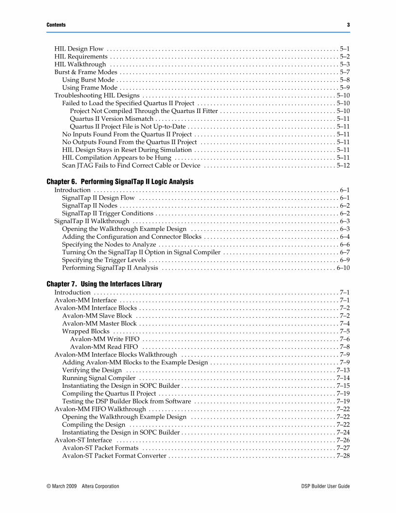
Add the Noise BlockPerform the following steps to add the Noise block:
1. Select the IO & Bus library from the Altera DSP Builder Blockset folder in the Simulink Library Browser.
2. Drag and drop an Input block into your model, positioning it to the right of the Random Bitstream block.
3. Click the text under the block icon in your model. Rename the block Noise.
4. Double-click the Noise block to display the Block Parameters dialog box.
5. Set the Noise block parameters as shown in Table 2–8.
1 The dialog box options change to display only the relevant options when you select a new bus type.
Figure 2–8. Setting Up the Random Number Generator
Table 2–8. Parameters for the Noise Block
Parameter Value
Bus Type Single Bit
Specify Clock Off

2–10 Chapter 2: Getting Started TutorialCreating the Amplitude Modulation Model
DSP Builder User Guide © March 2009 Altera Corporation
The completed dialog box is shown in Figure 2–9.
6. Click OK.
7. Draw a connection line from the right side of the Random Bitstream block to the left side of the Noise block.
Add the Bus Builder BlockThe Bus Builder block converts a bit to a signed bus. Perform the following steps to add the Bus Builder block:
1. Select the IO & Bus library from the Altera DSP Builder Blockset folder in the Simulink Library Browser.
2. Drag and drop a Bus Builder block into your model, positioning it to the right of the Noise block.
3. Double-click the Bus Builder block in your model to display the Block Parameters dialog box.
4. Set the Bus Builder block parameters as shown in Table 2–9.
Figure 2–9. Setting the 1-Bit Noise Input Port
Table 2–9. Parameters for the Bus Builder Block
Parameter Value
Bus Type Signer Integer
[number of bits].[] 2

Chapter 2: Getting Started Tutorial 2–11Creating the Amplitude Modulation Model
© March 2009 Altera Corporation DSP Builder User Guide
The completed dialog box is shown in Figure 2–10.
5. Click OK.
6. Draw a connection line from the right side of the Noise block to the top left side of the Bus Builder block.
Add the GND BlockPerform the following steps to add the GND block:
1. Select the IO & Bus library from the Altera DSP Builder Blockset folder in the Simulink Library Browser.
2. Drag and drop a GND block into your model, positioning it underneath the Noise block.
3. Draw a connection line from the right side of the GND block to the bottom left side of the Bus Builder block.
Add the Product BlockPerform the following steps to add the Product block:
1. Select the Arithmetic library from the Altera DSP Builder Blockset folder in the Simulink Library Browser.
2. Drag and drop a Product block into your model, positioning it to the right of the Bus Builder block and slightly above it. Leave enough space so that you can draw a connection line under the Product block.
3. Double-click the Product block to display the Block Parameters dialog box.
4. Set the Product block parameters as shown in Table 2–10.
Figure 2–10. Build a 2-Bit Signed Bus
Table 2–10. Parameters for the Product Block
Parameter Value
Bus Type Inferred
Number of Pipeline Stages 0

2–12 Chapter 2: Getting Started TutorialCreating the Amplitude Modulation Model
DSP Builder User Guide © March 2009 Altera Corporation
1 The bit width parameters are set automatically when you select Inferred bus type. The parameters in the Optional Ports and Settings tab of this dialog box can be left with their default values.
The completed dialog box is shown in Figure 2–11.
5. Click OK.
6. Draw a connection line from the top left of the Product block to the line between the Delay and SinDelay blocks.
Add the StreamMod and StreamBit BlocksPerform the following steps to add the StreamMod and StreamBit blocks:
1. Select the IO & Bus library from the Altera DSP Builder Blockset folder in the Simulink Library Browser.
2. Drag and drop two Output blocks into your model, positioning them to the right of the Product block.
3. Click the text under the block symbols in your model. Change the block instance names from Output and Output1 to StreamMod and StreamBit.
4. Double-click the StreamMod block to display the Block Parameters dialog box.
5. Set the StreamMod block parameters as shown in Table 2–11.
Figure 2–11. Product Block Parameters
Table 2–11. Parameters for the StreamMod Block
Parameter Value
Bus Type Signed Integer
[number of bits].[] 19
External Type Inferred

Chapter 2: Getting Started Tutorial 2–13Creating the Amplitude Modulation Model
© March 2009 Altera Corporation DSP Builder User Guide
The completed dialog box is shown in Figure 2–12.
6. Click OK.
7. Double-click the StreamBit block to display the Block Parameters dialog box (Figure 2–13).
8. Set the StreamMod block parameters as shown in Table 2–12.
Figure 2–12. Set a 19-Bit Signed Output Bus
Figure 2–13. Set a Single-Bit Output Bus
Table 2–12. Parameters for the StreamMod Block
Parameter Value
Bus Type Single Bit
External Type Inferred
2–14 Chapter 2: Getting Started TutorialCreating the Amplitude Modulation Model
DSP Builder User Guide © March 2009 Altera Corporation
9. Draw connection lines from the right side of the Product block to the left side of the StreamMod block, and from the right side of the Bus Builder block to the left side of the StreamBit block.
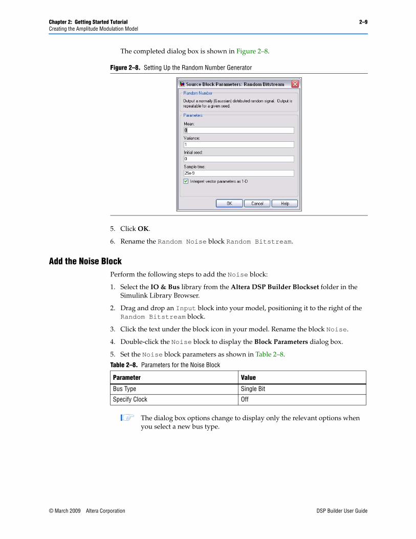
Add the Scope BlockPerform the following steps to add the Scope block:
1. Select the Simulink Sinks library in the Simulink Library Browser.
2. Drag and drop a Scope block into your model and position it to the right of the StreamMod block.
3. Double-click the Scope block and click the Parameters icon to display the ‘Scope’ parameters dialog box.
4. Set the Scope parameters as shown in Table 2–13.
The completed dialog box is shown in Figure 2–14.
5. Click OK.
6. Close the Scope.
7. Make connections to connect the complete your design as follows:
a. From the right side of the Mux block to the top left side of the Scope block.
b. From the right side of the StreamMod block to the middle left side of the Scope block.
Table 2–13. Parameters for the Scope Block
Parameter Value
Number of axes 3
Time range auto
Tick labels bottom axis only
Sampling Decimation 1
Figure 2–14. Display Three Signals in Time

Chapter 2: Getting Started Tutorial 2–15Creating the Amplitude Modulation Model
© March 2009 Altera Corporation DSP Builder User Guide
c. From the right side of the StreamBit block to the bottom left of the Scope block.
d. From the bottom left of the Product block to the line between the Bus Builder block and the StreamBit block.
Figure 2–15 shows the required connections.
Add a Clock BlockPerform the following steps to add a Clock block:
1. Select the AltLab library from the Altera DSP Builder Blockset folder in the Simulink Library Browser.
2. Drag and drop a Clock block into your model.
3. Double-click on the Clock block to display the Block Parameters dialog box (Figure 2–16 on page 2–16).
4. Set the Clock parameters as shown in Table 2–14.
1 A clock block is required to set a Simulink sample time that matches the sample time specified on the Sine Wave and Random Bitstream blocks. If no base clock exists in your design, a default clock with a 20ns real-world period and a Simulink sample time of 1 is automatically created.
5. Save your model.
Figure 2–15. Amplitude Modulation Design Example
Table 2–14. Parameters for the Clock Block
Parameter Value
Real-World Clock Period 20
Period Unit: ns
Simulink Sample Time 2.5e–008
Reset Name aclr
Reset Type Active Low
Export As Output Pin Off

2–16 Chapter 2: Getting Started TutorialSimulating the Model in Simulink
DSP Builder User Guide © March 2009 Altera Corporation
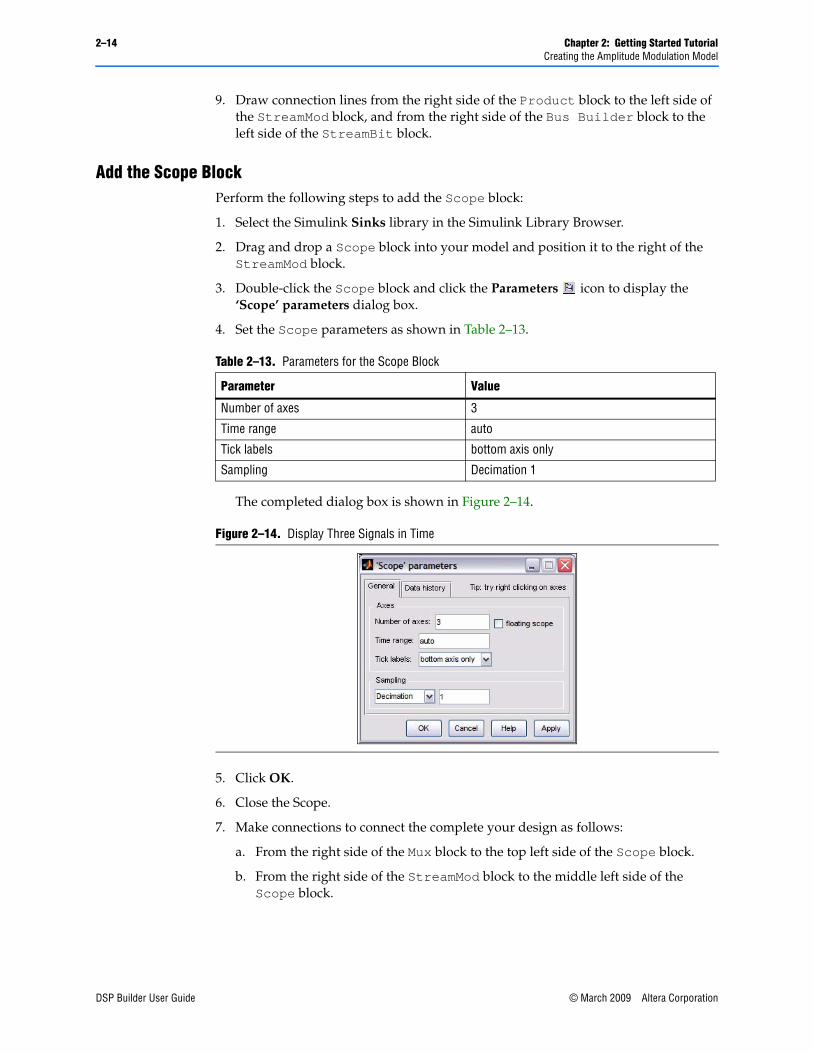
Simulating the Model in SimulinkTo simulate your model in the Simulink software, perform the following steps:
1. Click Configuration Parameters on the Simulation menu to display the Configuration Parameters dialog box and select the Solver page (Figure 2–17 on page 2–17).
2. Set the parameters shown in Table 2–15.
f For detailed information about solver options, refer to the description of the “Solver Pane” in the Simulink Help.
Figure 2–16. Clock Block Parameters Dialog Box
Table 2–15. Configuration Parameters for the singen Model
Parameter Value
Start time 0.0
Stop time 4e–6
Type Fixed-step
Solver discrete (no continuous states)
Chapter 2: Getting Started Tutorial 2–17Simulating the Model in Simulink
© March 2009 Altera Corporation DSP Builder User Guide
3. Click OK.
4. Start simulation by clicking Start on the Simulation menu.
5. Double-click the Scope block to view the simulation results.
6. Click the Autoscale icon (binoculars) to auto-scale the waveforms.
Figure 2–18 shows the scaled waveforms.
Figure 2–17. Configuration Parameters
Figure 2–18. Scope Simulation Results

2–18 Chapter 2: Getting Started TutorialCompiling the Design
DSP Builder User Guide © March 2009 Altera Corporation
Compiling the DesignTo create and compile a Quartus II project for your DSP Builder design, and to program your design onto an Altera FPGA, you must add a Signal Compiler block.
Perform the following steps:
1. Select the AltLab library from the Altera DSP Builder Blockset folder in the Simulink Library Browser.
2. Drag and drop a Signal Compiler block into your model.
3. Double-click the Signal Compiler block in your model to display the Signal Compiler dialog box (Figure 2–19).
The dialog box allows you to set the target device family. For this tutorial, you can use the default Stratix device family.
4. Click Compile.
Figure 2–19. Signal Compiler Block Dialog Box
Chapter 2: Getting Started Tutorial 2–19Performing RTL Simulation
© March 2009 Altera Corporation DSP Builder User Guide
5. When the compilation has completed successfully, click OK.
6. Click Save on the File menu to save your model.
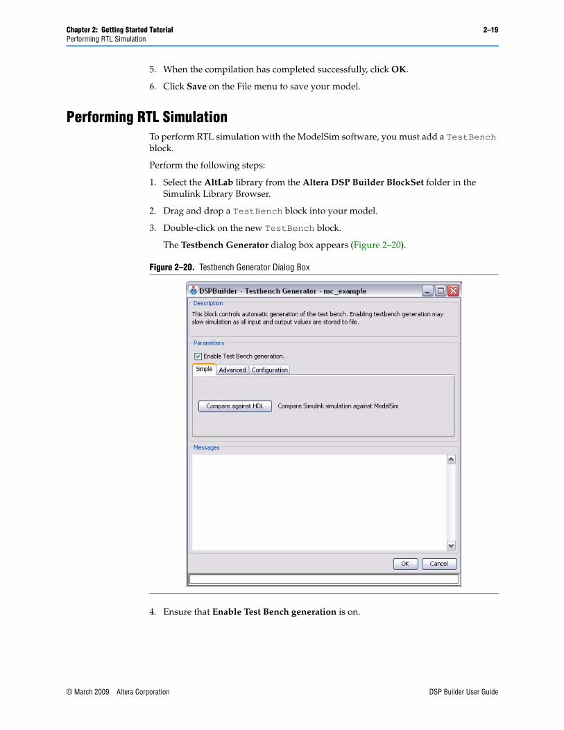
Performing RTL SimulationTo perform RTL simulation with the ModelSim software, you must add a TestBench block.
Perform the following steps:
1. Select the AltLab library from the Altera DSP Builder BlockSet folder in the Simulink Library Browser.
2. Drag and drop a TestBench block into your model.
3. Double-click on the new TestBench block.
The Testbench Generator dialog box appears (Figure 2–20).
4. Ensure that Enable Test Bench generation is on.
Figure 2–20. Testbench Generator Dialog Box

2–20 Chapter 2: Getting Started TutorialPerforming RTL Simulation
DSP Builder User Guide © March 2009 Altera Corporation
5. Click the Advanced tab (Figure 2–21).
6. Turn on the Launch GUI option. This option causes the ModelSim GUI to be launched when ModelSim simulation is invoked.
7. Click Generate HDL to generate a VDHL-based testbench from your model.
8. Click Run Simulink to generate Simulink simulation results for the testbench.
9. Click Run ModelSim to load your design into ModelSim.
Your design is simulated with the output displayed in the ModelSim Wave window.
1 All waveforms are initially shown using digital format in the ModelSim Wave window.
The testbench initializes all your design registers with a pulse on the aclr input signal.
10. Change the format of the sinin, sindelay and streammod signals to analog by selecting the signal name in the Wave window and right-clicking on Properties. In the Format tab, select Analog, and specify height 50, scale 0.001.
Figure 2–21. Testbench Generator Dialog Box Advanced Tab

Chapter 2: Getting Started Tutorial 2–21Adding the Design to a Quartus II Project
© March 2009 Altera Corporation DSP Builder User Guide
11. Click Zoom Full on the right button pop-up menu in the ModelSim Wave window. The simulation results display as an analog waveform similar to that shown in Figure 2–22.
You have now completed the introductory DSP Builder tutorial. The next section shows how you can add a DSP Builder design to a new or existing Quartus II project.
Subsequent chapters in this user guide provide walkthroughs that illustrate some of the additional design features supported by DSP Builder.
Adding the Design to a Quartus II ProjectThe Quartus II project created by the Signal Compiler block is used internally by DSP Builder. This section describes how to add your design to a new or existing Quartus II project.
Before following these steps, ensure that your design has been compiled using the Signal Compiler block as described in “Compiling the Design” on page 2–18.
Creating a Quartus II ProjectTo create a new Quartus II project, perform the following steps:
1. Start the Quartus II software.
2. Click New Project Wizard on the File menu in the Quartus II software and specify the working directory for your project. For example, D:\MyQuartusProject.
Figure 2–22. Analog Display

2–22 Chapter 2: Getting Started TutorialAdding the Design to a Quartus II Project
DSP Builder User Guide © March 2009 Altera Corporation
3. Specify the name of the project. For example, NewProject and the name of the top level design entity for the project.
1 The name of the top-level design entity typically has the same name as the project.
4. Click Next to display the Add Files page. There are no files to add for this tutorial.
5. Click Next to display the Family & Device Settings page and check that the required device family is selected. This should normally be the same device family as specified for Signal Compiler in “Compiling the Design” on page 2–18.
6. Click Finish to close the wizard and create the new project.
1 When you specify a directory that does not already exist, a message asks if the specified directory should be created. Click Yes to create the directory.
Add the DSP Builder Design to the ProjectTo add your DSP Builder design to the project in the Quartus II software:
1. On the View menu in the Quartus II software, point to Utility Windows and click Tcl Console to display the Tcl Console.
2. Run the <DSP Builder install path>\DesignExamples\Tutorials\ GettingStartedSinMdl\singen_add.tcl script in the Tcl Console by typing the following command:
# source <install path>/DesignExamples/Tutorials/GettingStartedSinMdl/ singen_add.tcl
1 You must use / separators instead of \ separators in the command path name used in the Tcl console window. You can use a relative path if you organize your design data with the DSP Builder and Quartus II designs in subdirectories of the same design hierarchy.
An example instantiation is added to your Quartus II project.
3. Click the Files tab in the Quartus II software.
4. Right-click singen.mdl and click Select Set as Top-Level Entity.
5. Compile the Quartus II design by clicking Start Compilation on the Processing menu.
1 You can copy the component declaration from the example file for your own code.

© March 2009 Altera Corporation DSP Builder User Guide
3. Design Rules and Procedures
DSP Builder Naming ConventionsDSP Builder generates VHDL files for simulation and synthesis. When there are blocks or ports in your model that share the same VHDL name, they are given unique names in the VHDL to avoid name clashes. However, clock and reset ports are never renamed, and an error is issued if they do not have unique names. Try to avoid name clashes on other ports, as this results in renaming of the top level ports in the VHDL.
All DSP Builder port names must comply with the following naming conventions:
■ VHDL is not case sensitive. For example, the input port MyInput and MYINPUT is the same VHDL entity.
■ Avoid using VHDL keywords for DSP Builder port names.
■ Do not use illegal characters. VHDL identifier names can contain only a - z, 0 - 9, and underscore (_) characters.
■ Begin all port names with a letter (a - z). VHDL does not allow identifiers to begin with non-alphabetic characters or end with an underscore.
■ Do not use two underscores in succession (__) in port names because it is illegal in VHDL.
1 White spaces in the names for the blocks/components and signals are converted to an underscore when Signal DSP Builder converts the Simulink model file (.mdl) into VHDL.
Using a MATLAB VariableYou can specify many block parameters (such as bit widths and pipeline depth) by entering a MATLAB base workspace or masked subsystem variable. These variables can then be set on the MATLAB command line or from a script. The variable is evaluated and its value passed to the simulation model files. Checks are performed to make sure that the parameters are in the required range. Values that can be set in this way are annotated as “Parameterizable” in the block parameter tables shown in the reference manual.
1 Although DSP Builder no longer restricts parameters to 51 bits, MATLAB evaluates parameter values to doubles. This restricts the possible values to 51-bit numbers expressible by a double.
f For information about which values are parameterizable, refer to the DSP Builder Reference Manual or to the block descriptions that can be accessed using the Help command in the right button pop-up menu for each block.

3–2 Chapter 3: Design Rules and ProceduresFixed-Point Notation
DSP Builder User Guide © March 2009 Altera Corporation
Fixed-Point NotationFigure 3–1 describes the fixed-point notation used for I/O formats in the DSP Builder block descriptions.
Figure 3–1 graphically compares the signed binary fractional, signed binary, and unsigned binary number formats.
Table 3–1. Fixed-Point Notation
Description NotationSimulink-to-HDL Translation
(Note 1), (Note 2)
Signed binary: fractional (SBF) representation; a fractional number
[L].[R] where:
■ [L] is the number of bits to the left of the binary point and the MSB is the sign bit
■ [R] is the number of bits to the right of the binary point
A Simulink SBF signal A[L].[R] maps in VHDL to STD_LOGIC_VECTOR({L + R - 1} DOWNTO 0)
Signed binary; integer (INT)
[L] where:
■ [L] is the number of bits of the signed bus and the MSB is the sign bit
A Simulink signed binary signal A[L] maps to STD_LOGIC_VECTOR({L - 1} DOWNTO 0)
Unsigned binary; integer (UINT)
[L] where:
■ [L] is the number of bits of the unsigned bus
A Simulink unsigned binary signal A[L] maps to STD_LOGIC_VECTOR({L - 1} DOWNTO 0)
Single bit integer (BIT)
[1] where:
■ the single bit can have values 1 or 0
A Simulink single bit integer signal maps to STD_LOGIC
Notes to Table 3–1:
(1) STD_LOGIC_VECTOR and STD_LOGIC are VHDL signal types defined in the (ieee.std_logic_1164.all and ieee.std_logic_signed.all IEEE library packages).
(2) For designs in which unsigned integer signals are used in Simulink, DSP Builder translates the Simulink unsigned bus type with width w into a VHDL signed bus of width w + 1 where the MSB bit is set to 0.
Figure 3–1. Number Format Comparison

Chapter 3: Design Rules and Procedures 3–3Fixed-Point Notation
© March 2009 Altera Corporation DSP Builder User Guide
Binary Point Location in Signed Binary Fractional FormatFor hardware implementation, Simulink signals must be cast into the desired hardware bus format. Therefore, floating-point values must be converted to fixed-point values.
This conversion is a critical step for hardware implementation because the number of bits required to represent a fixed-point value plus the location of the binary point affects both the amount of the hardware resources used and the system accuracy.
Choosing a large number of bits gives excellent accuracy—the fixed-point result is almost identical to the floating-point result—but consumes a large amount of hardware. You must design for the optimum size/accuracy trade-off. DSP Builder speeds up your design cycle by enabling simulation with fixed-point and floating-point signals in the same environment.
The Input block casts floating-point Simulink signals of type double into fixed-point signals. The fixed-point signals are represented in signed binary fractional (SBF) format as shown below:
■ [number of bits].[]—Represents the number of bits to the left of the binary point including the sign bit.
■ [].[number of bits]—Represents the number of bits to the right of the binary point.
In VHDL, the signals are typed as STD_LOGIC_VECTOR. Refer to (Note 1) in Table 3–1 on page 3–2.
For example, the 4-bit binary number 1101 is represented as:
Simulink This signed integer is interpreted as –3
VHDL This signed STD_LOGIC_VECTOR is interpreted as –3
If you change the location of the binary point to 11.01, that is, two bits on the left side of the binary point and two bits on the right side, the numbers are represented as:
Simulink This signed fraction is interpreted as –0.75
VHDL This signed STD_LOGIC_VECTOR is interpreted as –3
From a system-level analysis point of view, multiplying a number by –0.75 or –3 is very different, especially when looking at the bit width growth. In the first case, the multiplier output bus grows on the most significant bit (MSB), in the second case, the multiplier output bus grows on the least significant bit (LSB).
In both cases, the binary numbers are identical. However, the location of the binary point affects how a simulator formats the representation of the signal. For complex systems, you can adjust the binary point location to define the signal range and the area of interest.
f For more information on number systems, refer to AN 83: Binary Numbering Systems.

3–4 Chapter 3: Design Rules and ProceduresBit Width Design Rule
DSP Builder User Guide © March 2009 Altera Corporation
Bit Width Design RuleYou must specify the bit width at the source of the data path. DSP Builder propagates this bit width from the source to the destination through all intermediate blocks. Some intermediate DSP Builder blocks must have a bit width specified, while others have specific bit width growth rules which are described in the documentation for each block.
Some blocks which allow bit widths to be specified optionally, have an Inferred type setting that allows a growth rule to be used. For example, in the amplitude modulation tutorial design described in Chapter 2, Getting Started Tutorial, the SinIn and SinDelay blocks have a bit width of 16. Therefore, a bit width of 16 is automatically assigned to the intermediate Delay block.
Data Width PropagationYou can specify the bit width of many Altera blocks in the Simulink design. However, you do not need to specify the bit width for all blocks. If the bit width is not explicitly specified, DSP Builder assigns a bit width during the Simulink-to-VHDL conversion by propagating the bit width from the source of a data path to its destination.
Some intermediate DSP Builder blocks must have a bit width specified, while others have specific bit width growth rules which are described in the documentation for each block. Some blocks which allow bit widths to be specified optionally allow a growth rule to be used; this is the Inferred type setting.
The following design example illustrates bit-width propagation (Figure 3–2).
The fir3tapsub.mdl design is a 3-tap finite impulse response (FIR) filter and has the following attributes:
■ The input data signal is an 8-bit signed integer bus
■ The output data signal is a 20-bit signed integer bus
■ Three Delay blocks are used to build the tapped delay line
■ The coefficient values are {1.0000, -5.0000, 1.0000}, a Gain block performs the coefficient multiplication
Figure 3–2. 3-Tap FIR Filter

Chapter 3: Design Rules and Procedures 3–5Bit Width Design Rule
© March 2009 Altera Corporation DSP Builder User Guide
Figure 3–3 shows the RTL representation of fir3tapsub.mdl created by Signal Compiler.
Tapped Delay LineThe bit width propagation mechanism starts at the source of the data path, in this case at the Input block which is an 8-bit input bus. This bus feeds the register U0, which feeds U1, which feeds U2. DSP Builder propagates the 8-bit bus in this register chain where each register is eight bits wide (Figure 3–4).
Arithmetic OperationFigure 3–5 shows the arithmetic section of the filter, that computes the output yout:
where c[i] are the coefficients and x[k - i] are the data.
Figure 3–3. 3-Tap FIR Filter in Quartus II RTL View
Figure 3–4. Tap Delay Line in Quartus II Version RTL Viewer
yout k[ ] x k i–[ ]c i[ ]
i 0=
2
∑=
Figure 3–5. 3-Tap FIR Filter Arithmetic Operation in Quartus II Version RTL Viewer
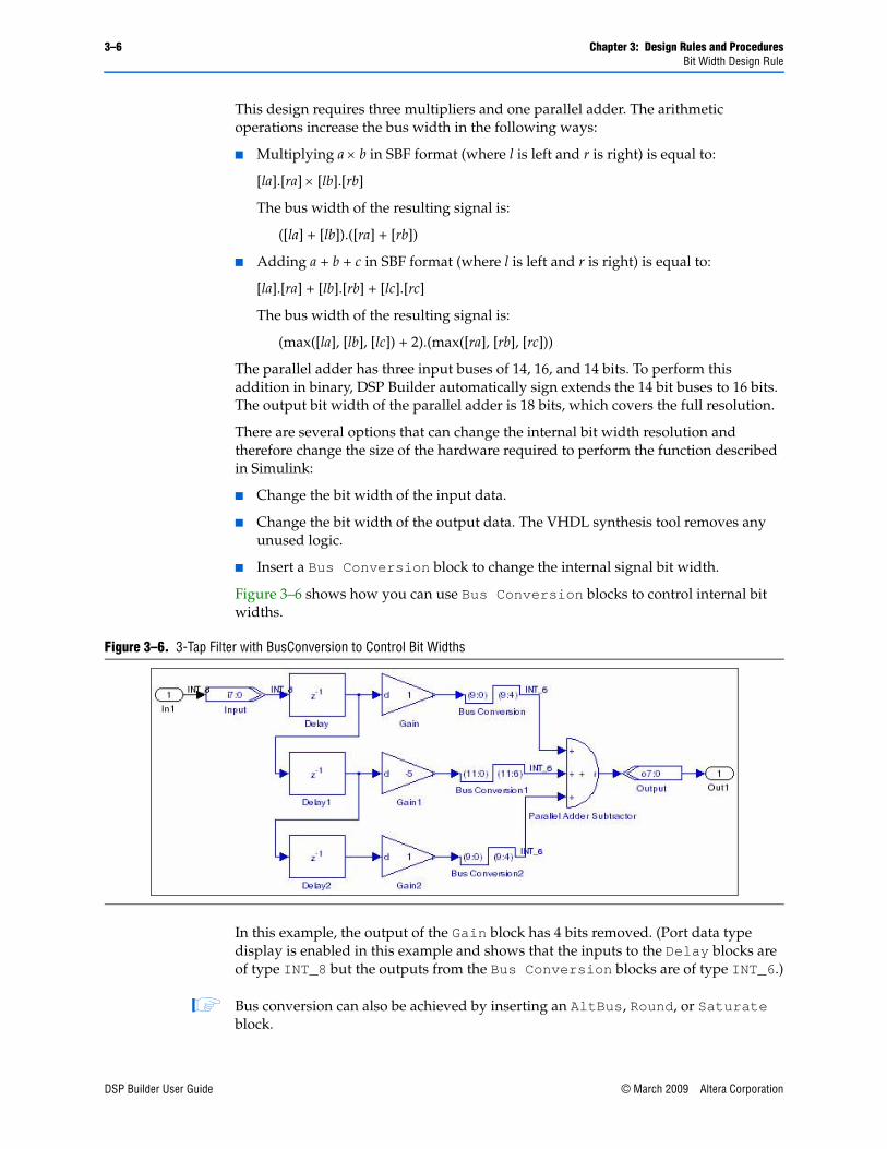
3–6 Chapter 3: Design Rules and ProceduresBit Width Design Rule
DSP Builder User Guide © March 2009 Altera Corporation
This design requires three multipliers and one parallel adder. The arithmetic operations increase the bus width in the following ways:
■ Multiplying a × b in SBF format (where l is left and r is right) is equal to:
[la].[ra] × [lb].[rb]
The bus width of the resulting signal is:
([la] + [lb]).([ra] + [rb])
■ Adding a + b + c in SBF format (where l is left and r is right) is equal to:
[la].[ra] + [lb].[rb] + [lc].[rc]
The bus width of the resulting signal is:
(max([la], [lb], [lc]) + 2).(max([ra], [rb], [rc]))
The parallel adder has three input buses of 14, 16, and 14 bits. To perform this addition in binary, DSP Builder automatically sign extends the 14 bit buses to 16 bits. The output bit width of the parallel adder is 18 bits, which covers the full resolution.
There are several options that can change the internal bit width resolution and therefore change the size of the hardware required to perform the function described in Simulink:
■ Change the bit width of the input data.
■ Change the bit width of the output data. The VHDL synthesis tool removes any unused logic.
■ Insert a Bus Conversion block to change the internal signal bit width.
Figure 3–6 shows how you can use Bus Conversion blocks to control internal bit widths.
In this example, the output of the Gain block has 4 bits removed. (Port data type display is enabled in this example and shows that the inputs to the Delay blocks are of type INT_8 but the outputs from the Bus Conversion blocks are of type INT_6.)
1 Bus conversion can also be achieved by inserting an AltBus, Round, or Saturate block.
Figure 3–6. 3-Tap Filter with BusConversion to Control Bit Widths
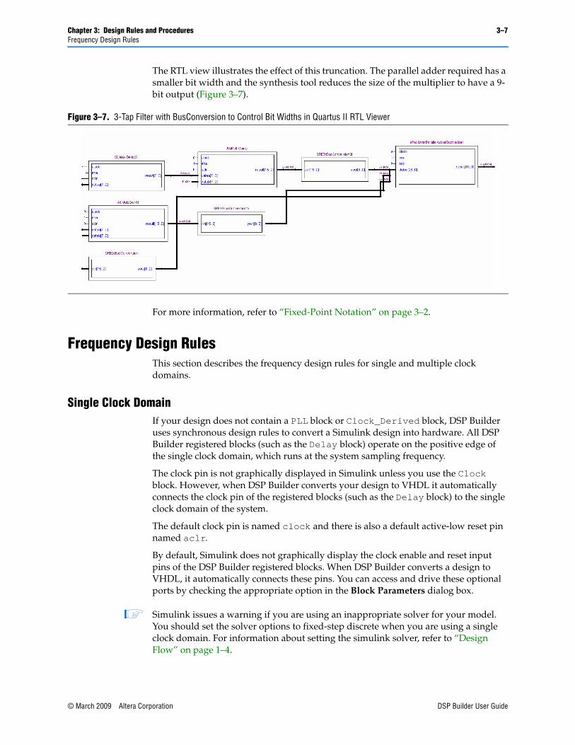
Chapter 3: Design Rules and Procedures 3–7Frequency Design Rules
© March 2009 Altera Corporation DSP Builder User Guide
The RTL view illustrates the effect of this truncation. The parallel adder required has a smaller bit width and the synthesis tool reduces the size of the multiplier to have a 9-bit output (Figure 3–7).
For more information, refer to “Fixed-Point Notation” on page 3–2.
Frequency Design RulesThis section describes the frequency design rules for single and multiple clock domains.
Single Clock DomainIf your design does not contain a PLL block or Clock_Derived block, DSP Builder uses synchronous design rules to convert a Simulink design into hardware. All DSP Builder registered blocks (such as the Delay block) operate on the positive edge of the single clock domain, which runs at the system sampling frequency.
The clock pin is not graphically displayed in Simulink unless you use the Clock block. However, when DSP Builder converts your design to VHDL it automatically connects the clock pin of the registered blocks (such as the Delay block) to the single clock domain of the system.
The default clock pin is named clock and there is also a default active-low reset pin named aclr.
By default, Simulink does not graphically display the clock enable and reset input pins of the DSP Builder registered blocks. When DSP Builder converts a design to VHDL, it automatically connects these pins. You can access and drive these optional ports by checking the appropriate option in the Block Parameters dialog box.
1 Simulink issues a warning if you are using an inappropriate solver for your model. You should set the solver options to fixed-step discrete when you are using a single clock domain. For information about setting the simulink solver, refer to “Design Flow” on page 1–4.
Figure 3–7. 3-Tap Filter with BusConversion to Control Bit Widths in Quartus II RTL Viewer

3–8 Chapter 3: Design Rules and ProceduresFrequency Design Rules
DSP Builder User Guide © March 2009 Altera Corporation
For Simulink simulation, all DSP Builder blocks (including registered DSP Builder blocks) use the sampling period specified in the Clock block. If there is no Clock block in your design, the DSP Builder blocks use a sampling frequency of 1. You can use the Clock block to change the Simulink sample period and the hardware clock period.
Multiple Clock DomainsA DSP Builder model can operate using multiple Simulink sampling periods. The clock domain can be specified in some DSP Builder block sources, such as the Counter block. The clock domain can also be specified in DSP Builder rate change blocks such as Tsamp.
When using multiple sampling periods, DSP Builder must associate each sampling period to a physical clock domain that can be available from an FPGA PLL or a clock input pin. Therefore, the DSP Builder model must contain DSP Builder rate change blocks such as PLL or Clock_Derived at the top level.
You can use a PLL block to synthesize additional clock signals from a reference clock signal. These internal clock signals are multiples of the system clock frequency. Table 3–3 on page 3–13 shows the number of PLL internal clock outputs supported by each device family.
If your design contains the PLL block, Clock or Clock_Derived blocks, the DSP Builder registered blocks operate on the positive edge of one of the block’s output clocks.
1 You must set a variable-step discrete solver in Simulink when you are using multiple clock domains. For information about setting the Simulink solver, refer to “Design Flow” on page 1–4.
To ensure a proper hardware implementation of a DSP Builder design using multiple clock domains, consider the following:
■ Do not use DSP Builder combinational blocks for rate transitions to ensure that the behavior of the DSP Builder Simulink model is identical to the generated RTL representation.
Figure 3–8 illustrates an incorrect use of the DSP Builder Logical Bit Operator (NOT) block.
Figure 3–8. Example of Incorrect Usage: Mixed Sampling Rate on a NOT Block

Chapter 3: Design Rules and Procedures 3–9Frequency Design Rules
© March 2009 Altera Corporation DSP Builder User Guide
■ Two DSP Builder blocks can operate with two different sampling periods. However for most DSP Builder blocks the sampling period of each input port and each output port must be identical.
Although this rule applies to a large majority of DSP Builder blocks, there are some exceptions such as the Dual-Clock FIFO block where the sampling period of the read input port is expected to be different than the sampling period of the write input port.
■ For a data path using mixed clock domains, additional register decoupling may be required around the register that is between the domains.
This requirement is especially true when the source data rate is higher than the destination register, in other words, when the data of a register is toggling at the higher rate than the register’s clock pin, as shown in Figure 3–9.
A stable hardware implementation is shown in Figure 3–10.
Figure 3–9. Data Toggling Faster than Clock
Figure 3–10. Stable Hardware Implementation

3–10 Chapter 3: Design Rules and ProceduresFrequency Design Rules
DSP Builder User Guide © March 2009 Altera Corporation
Using Clock and Clock_Derived BlocksDSP Builder maps the Clock and Clock_Derived blocks to two hardware device input pins; one for the clock input, and one for the reset input for the clock domain. A design may contain zero or one Clock block and zero or more Clock_Derived blocks.
If you use Clock_Derived blocks, and there is only one system clock, you must generate an appropriate clock signal for connection to the hardware device input pins for the derived clocks.
The Clock block defines the base clock domain, and Clock_Derived blocks define other clock domains whose sample times are specified in terms of the base clock sample time. If there is no Clock block, a default base clock is used, with a Simulink sample time of 1, and a hardware clock period of 20us.
This feature is available across all device families supported by DSP Builder. If no Clock block is present, a default clock pin named clock and a default active-low reset pin named aclr are used.
The Signal Compiler block assigns a clock buffer and a dedicated clock-tree to clock-signal input pin automatically to maintain minimum clock skew. If your design contains more Clock and Clock_Derived blocks than there are clock buffers available, non dedicated routing resources are used to route the clock signals.
Clock AssignmentDSP Builder identifies registered DSP Builder blocks such as the Delay block and implicitly connects the clock, clock enable, and reset signals in the VHDL design for synthesis. When your design does not contain a Clock block, Clock_Derived block, or PLL block, all the registered DSP Builder block clock pins are implicitly connected to a single clock domain (signal ‘clock’ in VHDL).
Clock domains are defined by the clock source blocks: the Clock block, the Clock_Derived block and the PLL block.
The Clock block defines the base clock domain. You can specify its Simulink sample time and hardware clock period directly. If there is no Clock block, there is a default base clock with a Simulink sample time of 1. You can use the Clock_Derived block to define clock domains in terms of the base clock. The sample time of a derived clock is specified as a multiple and divisor of the base clock sample time.
The PLL block maps to a hardware PLL. You can use it to define multiple clock domains with sample times specified in terms of the PLL input clock. The PLL input clock may be either the base clock or a derived clock.
Each clock domain has an associated reset pin. The Clock block and each of the Clock_Derived blocks have their own reset pin, which is named in the block's parameter dialog box. The clock domains of the PLL block share the reset pin of the PLL block's input clock.
When your design contains clock source blocks, DSP Builder implicitly connects the clock pins of all the registered blocks to the appropriate clock pin or PLL output. DSP Builder also connects the reset pins of the registered blocks to the top-level reset port for the block's clock domain.

Chapter 3: Design Rules and Procedures 3–11Frequency Design Rules
© March 2009 Altera Corporation DSP Builder User Guide
DSP Builder blocks fall into the following clocking categories:
■ Combinational blocks—The output always changes at the same sample time slot as the input.
■ Registered blocks—The output changes after a variable number of sample time slots.
Figure 3–11 illustrates DSP Builder block combinational behavior.
The Magnitude block translates as a combinational signal in VHDL. DSP Builder does not add clock pins to this function.
Figure 3–12 illustrates the behavior of a registered DSP block. In the VHDL netlist, DSP Builder adds clock pin inputs to this function. The Delay block, with the Clock Phase Selection parameter equal to 100, is converted into a VHDL shift register with a decimation of three and an initial value of zero.
Figure 3–11. Magnitude Block: Combinational Behavior
Figure 3–12. Delay Block: Registered Behavior

3–12 Chapter 3: Design Rules and ProceduresFrequency Design Rules
DSP Builder User Guide © March 2009 Altera Corporation
For feedback circuitry (that is, the output of a block fed back into the input of a block), a registered block must be in the feedback loop. Otherwise, an unresolved combinational loop is created (Figure 3–13).
You can design multi-rate designs by using the PLL block and assigning different sampling periods on registered DSP Builder blocks.
Alternatively, you can design multi-rate designs without the DSP Builder PLL block by using a single clock domain with clock enable and the following design rules:
■ The fastest sample rate is an integer multiple of the slower sample rates. The values are specified in the Clock Phase Selection field in the Block Parameters dialog box for the Delay block.
■ The Clock Phase Selection box accepts a binary pattern string to describe the clock phase selection. Each digit or bit of this string is processed sequentially on every cycle of the fastest clock. When a bit is equal to one, the block is enabled; when a bit is equal to zero, the block is disabled.
Table 3–2 shows some examples of typical clock phase selections.
Figure 3–13. Feedback Loop
Table 3–2. Clock Phase Selection Example
Phase Description
1 The Delay block is always enabled and captures all data passing through the block (sampled at the rate 1).
10 The Delay block is enabled every other phase and every other data (sampled at the rate 1) passes through.
0100 The Delay block is enabled on the 2nd phase out of 4 and only the 2nd data out of 4 (sampled at the rate 1) passes through. In other words, the data on phases 1, 3, and 4 do not pass through the Delay block.

Chapter 3: Design Rules and Procedures 3–13Frequency Design Rules
© March 2009 Altera Corporation DSP Builder User Guide
Figure 3–14 compares the scopes for the Delay block operating at a one quarter rate on the 1000 and 0100 phases, respectively.
Using the PLL BlockDSP Builder maps the PLL block to the hardware device PLL.
Table 3–3 shows the number of PLL internal clock outputs supported by each device family.
Figure 3–14. 1000 as Opposed to 0100 Phase Delay
Table 3–3. Device Support for PLL Clocks
Device Family Number of PLL Clocks
Stratix IV 9
Stratix III 9
Stratix II GX 6
Stratix II 6
Stratix GX 6
Stratix 6
Arria II GX 6
Arria GX 6
Cyclone III 5
Cyclone II 3
Cyclone 2

3–14 Chapter 3: Design Rules and ProceduresFrequency Design Rules
DSP Builder User Guide © March 2009 Altera Corporation
Figure 3–15 shows an example of multiple-clock domain support using the PLL block.
Figure 3–16 shows the clock setting configuration for the PLL block in the example design MultipleClockDelay.mdl. Output clock PLL_clk0 is set to 800 ns, and output clock PLL_clk1 is set to 100 ns.
Data path A (shown in green in Figure 3–15) operates on output clock PLL_clk0 and data path B (shown in red in Figure 3–15) operates on output clock PLL_clk1. These clocks are specified by setting the Specify Clock option and entering the clock name in the Block Parameter dialog box for each input block.
Figure 3–15. MultipleClockDelay.mdl
Figure 3–16. PLL Setting

Chapter 3: Design Rules and Procedures 3–15Timing Semantics Between Simulink and HDL Simulation
© March 2009 Altera Corporation DSP Builder User Guide
In this design, the Sample time parameters for the Sine Wave a block and Sine Wave b block are set explicitly to 1e-006 and 1e-007, so that data is provided to the input blocks at the rate at which they sample.
Using Advanced PLL FeaturesThe DSP Builder PLL block supports the fundamental multiplication and division factor for the PLL. If you want to use other PLL features (such as phase shift, duty cycle), do so in a separate Quartus II project using the following method:
■ Create a new Quartus II project and use the MegaWizard™ Plugin Manager to configure the ALTPLL block.
■ Add the DSP Builder .mdl file to the Quartus II project as a source file.
■ You can then create a top-level design that instantiates your ALTPLL variation and your DSP Builder design.
Timing Semantics Between Simulink and HDL SimulationDSP Builder uses the Simulink engine to simulate the behavior of hardware components. However, there are some fundamental differences between the step-based simulation in Simulink and the event-driven simulation used for VHDL and Verilog HDL designs.
DSP Builder bridges this gap by establishing a set of timing semantics for translating between the Simulink and HDL environments.
Simulink Simulation ModelThe Simulink timing mode recommended for use with DSP Builder is a discrete fixed-step simulation, to facilitate correlation between HDL and Simulink simulation. This is configured in the Configuration Parameters dialog box which is available from the Simulation menu in Simulink (Figure 1–2 on page 1–5). Each step is a discrete unit of simulation. The clock is quantized in an idealized manner as a cycle counter.
At the beginning of each step, Simulink provides each block with known inputs. Functions are evaluated and the resultant outputs are propagated in the current step. The outputs of your model are the results of all these computations.
For all steps, Simulink blocks produce output signals. Outputs varying based on inputs received in the same step are referred to as direct feedthrough. Some DSP Builder blocks may include direct feedthrough outputs, depending on the parameterization of each block.
HDL Simulation ModelsHardware simulation is driven by a clock signal and the availability of input stimuli. The testbench script generated by the TestBench block feeds input signals to the HDL simulator that maintain correlation between the HDL and Simulink simulation.
Simulation models in the DSP Builder libraries evaluate their logic on positive clock edges. To avoid any timing conflicts, external inputs transition on negative clock edges.
3–16 Chapter 3: Design Rules and ProceduresTiming Semantics Between Simulink and HDL Simulation
DSP Builder User Guide © March 2009 Altera Corporation
Registered outputs are updated on positive clock edges. TestBench block-generated inputs arrive on negative clock edges, causing an apparent half-cycle delay in the arrival of output as shown in Figure 3–17 on page 3–17.
Startup & Initial ConditionsThe testbench includes a global reset for each clock domain. All blocks (except the HDL Import and MegaCore function blocks) automatically connect any reset on the hardware to the global asynchronous reset for the clock domain.
When a block explicitly declares an asynchronous reset, this reset is ORed with the global reset.
A Global Reset block (SCLR), which corresponds to this hardware signal is provided in the Altera DSP Builder Blockset IO & Bus library.
The global reset signal is used as a reset prior to meaningful simulation. When converting from the Simulink domain to the hardware domain, the reset period is considered to be before the Simulink simulation begins. Therefore, in Simulink simulation, the Global Reset block outputs only a constant zero and has no simulation behavior. This means that the hardware is connected to reset, and thus reset at the start of a ModelSim testbench simulation.
1 DSP blocks or MegaCore functions may have additional initial conditions or startup states which are not automatically reset by the global reset signal.
DSP Builder Global Reset CircuitryBy default, Simulink does not graphically display the clock enable and reset input pins on DSP Builder registered blocks. When DSP Builder converts a design to HDL, it automatically connects the implied clock enable and reset pins.
If you turn on the optional ports in the Block Parameters dialog box for each of the DSP Builder registered blocks, you can access and drive the clock enable and reset input pins graphically in the Simulink software.
In the HDL domain, an asynchronous reset is used for the registered DSP Builder blocks, as shown in this behavioral VHDL code example:
process(CLOCK, RESET)begin
if RESET = '1' thendout <= (others => '0');
else if CLOCK'event and CLOCK = '1' thendout <= din;
end if;end
In addition, when targeting a development board, the Block Parameters dialog box for the DSP Board configuration block typically includes a Global Reset Pin selection box where you can choose from a list of pins that correspond to the DIP and push button switches.
The reset logic polarity can be either active-high or active-low. When active-low is selected, the value of the reset signal in Simulink simulation is still 0 for inactive and 1 for active. However, a NOT gate is inserted on the input pin in the hardware that is generated. The value of the reset signal in simulation is therefore the value as it exists across the internal design, rather then the value at the input pin.

Chapter 3: Design Rules and Procedures 3–17Timing Semantics Between Simulink and HDL Simulation
© March 2009 Altera Corporation DSP Builder User Guide
Quartus® II synthesis interprets this reset as an asynchronous reset, and uses an input of the logic element look-up table to instantiate the function. The HDL simulates correctly in this case because the testbench produces the reset input as required.
Reference Timing DiagramFigure 3–17 shows the timing relationships in a hypothetical case where a register is fed by the output of a counter. The counter output begins at 10, in other words, the value is 10 during the first Simulink clock step.
This timing is not true when crossing clock domains. For example, Figure 3–18 shows the timing delays introduced in a design with a derived clock that has half the base clock period. In general, DSP Builder is not cycle-accurate when crossing clock domains.
Figure 3–17. Single-Clock Timing Relationships
Figure 3–18. Multiple-Clock Timing Relationships

3–18 Chapter 3: Design Rules and ProceduresSignal Compiler and TestBench Blocks
DSP Builder User Guide © March 2009 Altera Corporation
Signal Compiler and TestBench BlocksThe Signal Compiler block uses Quartus II synthesis to convert a Simulink design into synthesizable VHDL including generation of a VHDL testbench and other supporting files for simulation and synthesis.
Signal Compiler assumes that your design complies with the Simulink rules and that any variables and inherited variables have been propagated through the whole design.
You should always run a simulation in Simulink before running Signal Compiler. The simulation updates all variables in your design (including workspace variables and inherited parameters), sets up certain blocks (such as the memory blocks, and inputs from and outputs to workspace blocks), and also traps any design errors that do not comply with Simulink rules.
The Input and Output blocks map to input and output ports in VHDL and mark the edge of the generated system. Typically, you connect these blocks to the Simulink simulation blocks for your testbench. An Output block should not connect to another Altera block. If you connect more Altera blocks (that map to HDL), empty ports are created and the HDL does not compile for synthesis.
f For more information on the Input and Output blocks, refer to the IO & Bus Library chapter of the DSP Builder Reference Manual.
Design Flows for Synthesis, Compilation and SimulationYou can use Signal Compiler to control your design flow for synthesis, compilation, and simulation. DSP Builder supports the following flows:
■ Automatic Flow—The automated flow allows you to control the entire design process in the MATLAB/Simulink environment using the Signal Compiler block. With this flow, your design is compiled inside a temporary Quartus II project. The results of the synthesis and compilation are displayed in the Signal Compiler Messages box. You can also use the automated flow to download your design into supported development boards.
■ Manual Flow—You can also add the .mdl file to an existing Quartus II project using the <model name>_add.tcl script. This script is generated whenever the Signal Compiler or TestBench block is run. You can use the script to add the .mdl file and any imported HDL to your project. You can then instantiate your design in HDL.
■ Simulation Flow—Use the TestBench block to compile your design for Modelsim simulation. For this to work, ModelSim must be on your path. You can automatically compare the Simulink and Modelsim simulation results.
For an example that uses the Signal Compiler blocker, refer to page 2–15 of the “Getting Started Tutorial”.
f For information about setting parameters for the Signal Compiler block, refer to the Signal Compiler section in the AltLab Library chapter of the DSP Builder Reference Manual.

Chapter 3: Design Rules and Procedures 3–19Hierarchical Design
© March 2009 Altera Corporation DSP Builder User Guide
Hierarchical DesignDSP Builder supports hierarchical design using the Simulink Subsystem block.
DSP Builder preserves the hierarchy structure in a VHDL design and each hierarchical level in a Simulink model file (.mdl) translates into one VHDL file.
For example, Figure 3–19 illustrates a hierarchy for a design fir3tap.mdl, which implements two FIR filters.
For information on naming the Subsystem block instances, refer to “DSP Builder Naming Conventions” on page 3–1.
Figure 3–19. Hierarchical Design Example

3–20 Chapter 3: Design Rules and ProceduresGoto and From Block Support
DSP Builder User Guide © March 2009 Altera Corporation
Goto and From Block SupportDSP Builder supports the Goto and From blocks from the Signal Routing folder in the generic Simulink library.
You can use these blocks for large fan-out signals and to enhance the diagram clarity.
Figure 3–20 shows an example of the Goto and From blocks.
The Goto blocks ([ReadAddr], [WriteAddr], and [WriteEna] are used with the From blocks ([ReadAddr], [WriteAddr], and [WriteEna], which are connected to the dual-port RAM blocks.
Figure 3–20. Goto & From Block Example

Chapter 3: Design Rules and Procedures 3–21Black Boxing and HDL Import
© March 2009 Altera Corporation DSP Builder User Guide
Black Boxing and HDL ImportYou can add your own VHDL or Verilog HDL code to your design and specify which subsystem block(s) should be translated into VHDL by DSP Builder. This process, called black boxing, can be implemented implicitly or explicitly.
An explicit black box uses the HDL Input, HDL Output, HDL Entity, and Subsystem Builder blocks. For information on using these blocks to create an explicit black box, refer to “Subsystem Builder Walkthrough” in Chapter 8.
An implicit black box uses the HDL Import block to instantiate the black box subsystem. For information on implicit black boxing using your own HDL code, refer to the “HDL Import Walkthrough” in Chapter 8.
Using a MATLAB Array or HEX File to Initialize a BlockYou can use a MATLAB array to specify the values entered in the LUT block or to initialize the Dual-Port RAM, Single-Port RAM, True Dual-Port RAM, or ROM blocks. You can also use an Intel format HEX file to initialize a RAM or ROM block.
If the data values specified by the MATLAB array or HEX file are not exactly representable in the selected data type, they are rounded and a warning is issued. The values are rounded by expressing the number in binary format, then truncating to the specified width. This results in rounding towards minus infinity.
For example, if the input value is –0.25 (minimally expressed in signed binary fractional two’s compliment format as 111) and the selected target data format is signed fractional [1].[1], then the value is truncated to 11 = –0.5. The value is rounded towards minus infinity to the nearest representable number.
Similarly, if you select unsigned integer data type and the value is 1.9, this is rounded down to 1.
Comparison UtilityDSP Builder provides a simple utility that runs simulation comparison between Simulink and ModelSim from the command line:
alt_dspbuilder_verifymodel('modelname.mdl', 'logfile.txt')rA testbench GUI is displays messages as the comparison is performed. The command returns true (1) or false (0) according to whether the simulation results match and the output is recorded in the specified log file.
For more information on running a comparison between Simulink and ModelSim, refer to “Performing RTL Simulation” in Chapter 2.
Adding Comments to BlocksYou can add comments to any DSP Builder block by right-clicking on the block to display the Block Properties dialog box and entering text in the Description field of the dialog box as shown in Figure 3–21.

3–22 Chapter 3: Design Rules and ProceduresAdding Quartus II Constraints
DSP Builder User Guide © March 2009 Altera Corporation
The comment text is included next to the instantiation of the block in the generated HDL.
Adding Quartus II ConstraintsYou can set Quartus II global project assignments in your Simulink model by adding Quartus II Global Project Assignment blocks from the AltLab library. Each block sets a single global assignment but you can use multiple blocks for multiple assignments. You can use these assignments to set Quartus II compilation directives, such as target device or timing requirements.
f For a description of the Quartus II Global Project Assignment block, refer to the DSP Builder Reference Manual.
You can add additional Quartus II assignments or constraints that are not supported in DSP Builder by creating a Tcl script in your design directory. Any file named <model name>_add_user.tcl is automatically sourced when you run Signal Compiler.
The Tcl file can include any number of Quartus II assignments with the syntax:
set_global_assignment -name <assignment> <value>
f For detailed information about Quartus II assignments, refer to the Quartus II Settings File Reference Manual.
Figure 3–21. Adding Comments to a Block

Chapter 3: Design Rules and Procedures 3–23Displaying Port Data Types
© March 2009 Altera Corporation DSP Builder User Guide
Displaying Port Data TypesYou can optionally display the Simulink and DSP Builder port data types for each of the signals in your Simulink model by turning on Port Data Types in the Port/Signal Displays section of the Simulink Format menu.
When this option is set, the DSP Builder internal signal type (SBF_L_R, INT_L, UINT_L, or BIT where L, and R are the number of bit to the left and right of the binary point) is displayed. For example, SBF_8_4 for a 12-bit signed binary fractional data type with 4 fractional bits, or UINT_16 for a 16-bit unsigned integer.
Figure 3–22 shows the Amplitude Modulation example from the Getting Started Tutorial with port data type display enabled.
For more information about the DSP Builder internal signal types, refer to “Fixed-Point Notation” on page 3–2.
Displaying the Pipeline DepthYou can optionally display the pipeline depth on the primitive blocks (such as the Arithmetic library blocks) in your Simulink model by adding a Display Pipeline Depth block from the AltLab library.
You can change the display mode by double-clicking on the block. When set, the current pipeline depth is displayed at the top right corner of each block that adds latency to your design as shown in Figure 3–22. The selected mode is shown on the Display Pipeline Depth block symbol.
Updating HDL Import BlocksThe HDL Import blocks in your design may need updating if you have upgraded from a previous software version or have moved a design to a different workstation.
Figure 3–22. Tutorial Example Showing Port Data Types and Pipeline Depth

3–24 Chapter 3: Design Rules and ProceduresAnalyzing the Hardware Resource Usage
DSP Builder User Guide © March 2009 Altera Corporation
You can use the alt_dspbuilder_refresh_hdlimport command to update these blocks. This command checks that the referenced HDL files (or Quartus II project) exists. If found, the HDL Import dialog box is opened and a compilation is automatically invoked to regenerate the Simulink model. If neither is found, but there is an existing simulation netlist, this netlist is used for simulation.
To run the command, perform the following steps:
1. Start the MATLAB/Simulink software.
2. Open a Simulink model that contains imported HDL.
3. Run the command by typing the following at the MATLAB prompt:
alt_dspbuilder_refresh_hdlimport rYou can optionally select a HDL Import block to run the command on only the selected subsystem.
Analyzing the Hardware Resource UsageYou can analyze the hardware resources required for your design by using a Resource Usage block.
Perform the following steps:
1. Select the AltLab library from the Altera DSP Builder BlockSet folder in the Simulink Library Browser.
2. Drag and drop a Resource Usage block into your model and double-click on the block to open the Resource Usage dialog box.
3. Double-click on the Signal Compiler block and click Compile to re-compile your design in the Quartus II software.
The Resource Usage block is updated to show a summary of the estimated logic, RAM and DSP block usage (Figure 3–23).
The Resource Usage dialog box is updated to show a detailed report of the resources required by each of the blocks in your model that generate hardware.
Figure 3–23. Resource Usage Block

Chapter 3: Design Rules and Procedures 3–25Analyzing the Hardware Resource Usage
© March 2009 Altera Corporation DSP Builder User Guide
For example, Figure 3–24 shows the hardware resources required by the Product block in the Amplitude Modulation example from the Getting Started Tutorial.
f The information displayed depends on the selected device family. Refer to the device documentation for more information.
You can also click the Timing tab and click Highlight path to highlight the critical paths on your design.
1 When the source and destination shown in the dialog box are the same and a single block is highlighted, the critical path is due to the internal function or a feedback loop. For a more complex example, the entire critical path through your design may be highlighted.
Figure 3–24. Resource Usage Dialog Box

3–26 Chapter 3: Design Rules and ProceduresLoading Additional ModelSim Commands
DSP Builder User Guide © March 2009 Altera Corporation
Loading Additional ModelSim CommandsWhen you import HDL as a black box, DSP Builder creates a subdirectory named DSPBuilder<model name>_import. Any Tcl script named *_add_msim.tcl in this subdirectory is automatically sourced when you launch ModelSim.
You should not modify the generated scripts, but you can create you own scripts such as <user name>_add_msim.tcl which contain additional ModelSim commands that you want to load into ModelSim.
Making Quartus II Assignments to Block Entity NamesThe VHDL entity names of the blocks in a DSP Builder design are dependent on the block’s parameter values. This means that blocks of the same type and same parameterization share a common VHDL entity.
The entity names have the following format:
<block type name>_GN<8 alphanumeric characters>
For example, a Delay block entity name might be:
alt_dspbuilder_delay_GNLVAGVO3B
Changing the parameterization of the block causes the entity name to change. If you want to make an assignment to a block in the Quartus II project, and for the assignment to remain when the block parameters are changed, you can use regular expressions in the assignments.
For example, you may want to make a Preserve Registers assignment to the Delay blocks in Figure 3–25 to prevent them from being merged.
Using the Quartus II Assignment Editor and Node Finder tools, you can identify the names of the registers and make the assignments to them. For example, if your model is named my_model, the names might be:
my_model_GN:auto_inst|alt_dspbuilder_delay_GNLVAGVO3B:Delay|alt_dspbuilder_SDelay:Delay1i|DelayLine
my_model_GN:auto_inst|alt_dspbuilder_delay_GNLVAGVO3B:Delay1|alt_dspbuilder_SDelay:Delay1i|DelayLine
Figure 3–25. Entity Name Assignment Example

Chapter 3: Design Rules and Procedures 3–27Making Quartus II Assignments to Block Entity Names
© March 2009 Altera Corporation DSP Builder User Guide
These assignments prevent merging of the registers. If you change the length of the delay, the assignments are no longer valid. However, you can edit the To field of the assignment and use a regular expression that is still valid if the entity name changes due to a parameter change: Replace the eight alphanumeric characters following the GN in the block entity name with .{8}, which is a regular expression that matches any eight characters. The targets of the assignments then become:
my_model_GN:auto_inst|alt_dspbuilder_delay_GN.{8}:Delay|alt_dspbuilder_SDelay:Delay1i|DelayLine
my_model_GN:auto_inst|alt_dspbuilder_delay_GN.{8}:Delay1|alt_dspbuilder_SDelay:Delay1i|DelayLine
If you want the assignment to apply to the whole block, not just the specific nodes, you can use the following code:
my_model_GN:auto_inst|alt_dspbuilder_delay_GN.{8}:Delay
my_model_GN:auto_inst|alt_dspbuilder_delay_GN.{8}:Delay1
Figure 3–26 shows this example in the Quartus II Assignment Editor.
You might want to do this if you are making the assignment to a more complicated block that contains many registers, and you want the assignment to apply to them all.
Figure 3–26. Preserve Registers Assignment in the Quartus II Assignment Editor

3–28 Chapter 3: Design Rules and ProceduresMaking Quartus II Assignments to Block Entity Names
DSP Builder User Guide © March 2009 Altera Corporation

© March 2009 Altera Corporation DSP Builder User Guide
4. Using MegaCore Functions
IntroductionAltera provides a number of parameterizable intellectual property (IP) MegaCore functions that you can integrate into the Simulink model of your DSP Builder designs.
The OpenCore Plus evaluation feature allows you to download and evaluate these MegaCore functions in hardware and simulation prior to licensing.
The following MegaCore functions are available in DSP Builder:
■ CIC (cascaded integrator-comb) filter
■ FFT (fast Fourier transform)
■ FIR (finite impulse response) filter compiler
■ NCO (numerically controlled oscillator)
■ Reed Solomon error correction compiler
■ Viterbi decoder compiler.
These MegaCore functions are represented by blocks in the MegaCore Functions library of the Altera DSP Builder Blockset in the Simulink Library Browser.
You must parameterize and generate these MegaCore functions after you add one of these blocks to your model. Refer to “MegaCore Function Walkthrough” on page 4–4 for an example of the design flow using these MegaCore functions.
Installing MegaCore FunctionsAltera DSP MegaCore functions are installed with the Quartus® II software. Refer to the MegaCore function user guides for information about each MegaCore function.
It is important to run the DSP Builder MegaCore function setup command after the installation of new MegaCore functions. This updates DSP Builder for all newly installed or upgraded MegaCore functions.
To run this setup command, follow these steps:
1. Start the MATLAB software. (If MATLAB is already running, check that the Simulink library browser is closed.)
2. Use the cd command at the MATLAB prompt to change directory to the directory where DSP Builder was installed.
3. Run the setup command by typing the following at the MATLAB prompt:
alt_dspbuilder_setup_megacore r
1 The process of building the MegaCore function blocks can take several minutes. Do not close MATLAB before the process has completed. Any messages of the form “Cannot find the declaration of element 'entity'.“are expected when installing a new MegaCore library and can be ignored.

4–2 Chapter 4: Using MegaCore FunctionsUpdating MegaCore Function Variation Blocks
DSP Builder User Guide © March 2009 Altera Corporation
Running this command, creates a MegaCore Functions subfolder below the Altera DSP Builder Blockset in the Simulink Library Browser.
In this folder, there should be a blue block with a version name for each of the installed MegaCore functions.
Updating MegaCore Function Variation BlocksAlthough a DSP Builder design using MegaCore function blocks from the MegaCore Functions library can be translated by Signal Compiler into a VHDL or Verilog HDL model, a MegaCore function variation block always uses an intermediate VHDL file to record parameters.
These blocks may revert to their unconfigured appearance if the VHDL file which describes the function variation is available but the simulation database (.simdb) file is not. A block may also require updating if you have changed the version of the MegaCore function you are using.
In these cases, you can update the MegaCore function variation blocks in your design using the alt_dspbuilder_refresh_megacore command.
This command recreates the simulation files based on the VHDL file for each MegaCore function block in the current Simulink model.
1 A Quartus II license must be available on the machine for the command to execute without errors.
To run the command, perform the following steps:
1. Start the MATLAB/Simulink software.
2. If necessary, use the cd command at the MATLAB prompt to change directory to your project directory.
3. Run the command by typing the following at the MATLAB prompt:
alt_dspbuilder_refresh_megacore r
Using Previous Versions of MegaCore FunctionsThe current MegaCore IP library is installed automatically with the Quartus II software and is detected because it is found at <QUARTUS_ROOTDIR>/../ip.
Any MegaCore function installed independently of the Quartus II software (prior to Quartus II v8.0) is also detected automatically.
It is also possible to use MegaCore functions that were installed automatically with previous versions of the Quartus II software (Quartus II v8.0 and later). To use these MegaCore functions, the previous IP MegaCore library directory and all its contents can be copied from the old Quartus II installation to a location below the ip directory in the current installation (for example: <QUARTUS_ROOTDIR>/../ip/ip_81).
It is then necessary to execute the alt_dspbuilder_setup_megacore command to ensure these cores are detected by DSP Builder.

Chapter 4: Using MegaCore Functions 4–3Design Flow Using MegaCore Functions
© March 2009 Altera Corporation DSP Builder User Guide
Design Flow Using MegaCore FunctionsUsing MegaCore functions in the MATLAB/Simulink environment is a five-step process.
1. Add the MegaCore function to the Simulink model and give the block a unique name.
2. Parameterize the MegaCore function variation.
3. Generate the MegaCore function variation.
4. Connect your MegaCore function variation to the other blocks in your model.
5. Simulate the MegaCore function variation in your model.
f Refer to the appropriate MegaCore function user guide for information about the design flow used for each MegaCore function.
Placing the MegaCore Function in the Simulink ModelYou can add a MegaCore function to a Simulink model by dragging a copy of the block from the Simulink Library Browser to your design workspace like any other Simulink block.
The default name of a MegaCore function block includes its version number. If you add more than one copy of a block in the same model, this number is automatically incremented to make the name unique. (The correct version number is still shown on the body of the block.) Altera recommends that you rename all blocks representing MegaCore functions with a name describing their use in your design. Using unique block names ensures that all the generated entities for the same MegaCore function in a hierarchical design also have unique names.
After adding the block and before parameterization, save your model file.
Parameterizing the MegaCore Function VariationDouble-click the MegaCore function block to open the IP Toolbench or MegaWizard interface.
1 You can also double-click on a block to re-open and modify a previously parameterized MegaCore function variation.
Generating the MegaCore Function VariationYou must generate a MegaCore function variation after you have parameterized the MegaCore function before you can connect the block to your design.
Click Generate in IP Toolbench (or Finish in the MegaWizard interface) to generate the necessary files for your MegaCore function variation.
DSP Builder also performs an additional step of optimizing your model for use in Simulink. This process may take up to a few minutes to complete depending on the complexity of the MegaCore function variation.

4–4 Chapter 4: Using MegaCore FunctionsMegaCore Function Walkthrough
DSP Builder User Guide © March 2009 Altera Corporation
Connecting the MegaCore Function Variation Block to the DesignThe Simulink block now has the required input and output ports as parameterized in IP Toolbench or the MegaWizard interface. These ports can be connected to other Altera DSP Builder blocks in your Simulink design.
Simulating the MegaCore Function Variation in the ModelThe Simulink block representing the MegaCore function variation can be simulated like any other block from the Simulink Library Browser.
1 Ensure that the Simulink simulation engine is set to use the discrete solver by selecting fixed-step type under Solver Options in the Configuration Parameters dialog box.
You should reset the MegaCore function at the start of the simulation to avoid any functional discrepancy between RTL simulation and Simulink simulation, as described in “Startup & Initial Conditions” on page 3–16.
MegaCore Function WalkthroughThis walkthrough shows how to create a custom low-pass FIR filter MegaCore function variation using the IP Toolbench interface.
1 This walkthrough assumes that the Altera MegaCore IP Library is installed.
Creating a New Simulink ModelCreate a new Simulink workspace by performing the following steps:
1. Start the MATLAB/Simulink software.
2. On the File menu, point to New and click Model to create a new model window.
3. Click Save on the File menu in the new model window.
4. Browse to the directory in which you want to save the file. This directory becomes your working directory. This walkthrough creates and uses the working directory <DSP Builder install path>\DesignExamples\Tutorials\MegaCore
5. Type the file name into the File name box. This walkthrough uses the name mc_example.mdl.
6. Click Save.
Adding the FIR Compiler FunctionTo place a FIR Compiler MegaCore function block in your design, perform the following steps:
1. On the View menu In your Simulink model window, click Library Browser. The Simulink Library Browser is displayed.
2. Select the MegaCore Functions library from the Altera DSP Builder Blockset folder in the Simulink Library Browser (Figure 4–1 on page 4–5).

Chapter 4: Using MegaCore Functions 4–5MegaCore Function Walkthrough
© March 2009 Altera Corporation DSP Builder User Guide
1 If the latest versions of the MegaCore function blocks do not appear as shown in Figure 4–1, make sure that the MegaCore IP Library, including the FIR Compiler MegaCore function is installed correctly. For instructions on installing the MegaCore IP library, refer to “Installing MegaCore Functions” on page 4–1.
3. Drag and drop a blue versioned fir_compiler_v9.0 block into your model as shown in Figure 4–2.
Figure 4–1. MegaCore Functions Library
Figure 4–2. FIR Compiler Block Placed in Simulink Model

4–6 Chapter 4: Using MegaCore FunctionsMegaCore Function Walkthrough
DSP Builder User Guide © March 2009 Altera Corporation
The block is added with a default instance name which includes the version string. This name is automatically made unique if you add more than one instance of the same block. However, you may want to change the name to be more meaningful in your design.
4. For this tutorial, rename the block to my_fir_compiler. To rename the block, click the default name (the text outside of the block itself) and edit the text. Naming conventions are described in “DSP Builder Naming Conventions” on page 3–1.
1 Always give blocks representing your MegaCore function variations unique names, to avoid issues caused by two or more entities in a hierarchical design.
Parameterizing the FIR Compiler FunctionTo use FIR Compiler to create a MegaCore function variation that fits the specific needs of your design, perform the following steps:
1. Double-click the my_fir_compiler block to start IP Toolbench (Figure 4–3).
2. Click Step 1: Parameterize to specify how the FIR filter should operate.
Figure 4–3. IP Toolbench-Parameterize
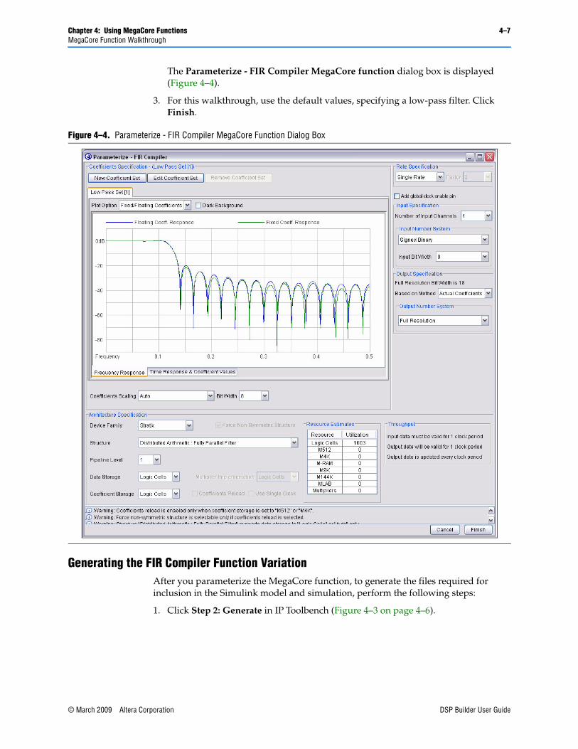
Chapter 4: Using MegaCore Functions 4–7MegaCore Function Walkthrough
© March 2009 Altera Corporation DSP Builder User Guide
The Parameterize - FIR Compiler MegaCore function dialog box is displayed (Figure 4–4).
3. For this walkthrough, use the default values, specifying a low-pass filter. Click Finish.
Generating the FIR Compiler Function VariationAfter you parameterize the MegaCore function, to generate the files required for inclusion in the Simulink model and simulation, perform the following steps:
1. Click Step 2: Generate in IP Toolbench (Figure 4–3 on page 4–6).
Figure 4–4. Parameterize - FIR Compiler MegaCore Function Dialog Box
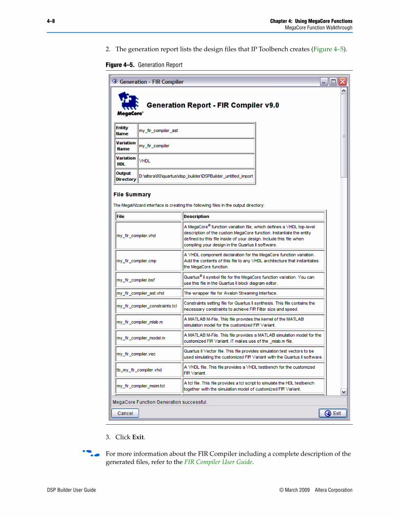
4–8 Chapter 4: Using MegaCore FunctionsMegaCore Function Walkthrough
DSP Builder User Guide © March 2009 Altera Corporation
2. The generation report lists the design files that IP Toolbench creates (Figure 4–5).
3. Click Exit.
f For more information about the FIR Compiler including a complete description of the generated files, refer to the FIR Compiler User Guide.
Figure 4–5. Generation Report

Chapter 4: Using MegaCore Functions 4–9MegaCore Function Walkthrough
© March 2009 Altera Corporation DSP Builder User Guide
The my_fir_compiler block in the Simulink model is updated to show the input and output ports for the given configuration (Figure 4–6).
The FIR filter is ready to be connected to the rest of your Simulink design.
Adding Stimulus and Scope BlocksIn this section, you create a sample design to test the low-pass filter by feeding the filter two sine waves as shown in Figure 4–7 on page 4–11.
For information on how to add blocks to a design and modify their parameters, refer to Chapter 2, Getting Started Tutorial.
Perform the following steps:
1. Add two Sine Wave blocks (from the Simulink Sources library).
1 Notice that the second block is automatically given a unique name.
2. Use the Block Parameters dialog box to set the parameters for the Sine Wave block shown in Table 4–1.
3. Repeat Step 2 for the Sine Wave1 block.
4. Connect the outputs from the Sine Wave and Sine Wave1 blocks to an Add block (from the Simulink Math Operations library).
5. Add an Input block (from the IO & Bus library in the Altera DSP Builder Blockset) and connect it between the Add block and the ast_sink_data pin on the my_fir_compiler block.
Figure 4–6. FIR Compiler Block in Simulink Model After Generation
Table 4–1. Parameters for the Sine Wave Blocks
Parameter
Value
Sine Wave Sine Wave1
Sine type Sample based Sample based
Time Use simulation time Use simulation time
Amplitude 64 64
Bias 0 0
Samples per period 200 7
Number of offset examples 0 0
Sample time 1 1
Interpret vector parameters as 1-D On On

4–10 Chapter 4: Using MegaCore FunctionsMegaCore Function Walkthrough
DSP Builder User Guide © March 2009 Altera Corporation
6. Use the Block Parameters dialog box to set the parameters shown in Table 4–2.
7. Add a Constant block (from the IO & Bus library) and connect this block to both the ast_sink_valid and ast_source_ready pins on the my_fir_compiler block.
8. Add another Constant block (from the IO & Bus library) and connect this block to the ast_sink_error pin on the my_fir_compiler block.
9. Use the Block Parameters dialog box to set the parameters for the Constant block shown in Table 4–3.
10. Repeat Step 9 for the Constant1 block.
11. Add a Single Pulse block (from the Gate & Control library in the Altera DSP Builder Blockset) and connect it to the reset_n pin on the my_fir_compiler block.
12. Use the Block Parameters dialog box to set the parameters shown in Table 4–4.
13. Add an Output block (from the IO & Bus library in the Altera DSP Builder Blockset) to your design and connect it to the ast_source_data pin on the my_fir_compiler block.
14. Use the Block Parameters dialog box to set the parameters shown in Table 4–5 on page 4–11.
Table 4–2. Parameters for the Input Block
Parameter Value
Bus Type Signed Integer
[number of bits].[] 8
Specify Clock Off
Table 4–3. Parameters for the Constant Blocks
Parameter
Value
Constant Constant1
Constant Value 1 0
Bus Type Single Bit Signed Integer
[Number of Bits].[] – 2
Rounding Mode Truncate Truncate
Saturation Mode Wrap Wrap
Specify Clock Off Off
Table 4–4. Parameters for the Single Pulse Block
Parameter Value
Signal Generation Type Step Up
Delay 50
Specify Clock Off

Chapter 4: Using MegaCore Functions 4–11MegaCore Function Walkthrough
© March 2009 Altera Corporation DSP Builder User Guide
15. Add a Scope block (from the Simulink Sinks library). Use the ‘Scope’ Parameters dialog box to configure the Scope block as a 2-input scope.
16. Connect the Scope block to the Input and Output blocks to monitor the source noise data and the filtered output.
Your model should look similar to that shown in Figure 4–7.
Simulating the Design in SimulinkTo simulate your design, perform the following steps:
1. On the Simulation menu in your model, click Configuration Parameters to display the Configuration Parameters dialog box (Figure 4–8 on page 4–12).
2. Select the Solver page and set the parameters shown in Table 4–6.
f For detailed information about solver options, refer to the description of the “Solver Pane” in the Simulink Help.
3. Click OK.
Table 4–5. Parameters for the Output Block
Parameter Value
Bus Type Signed Integer
[number of bits].[] 18
External Type Inferred
Figure 4–7. Connecting Blocks to the Low-Pass Filter
Table 4–6. Configuration Parameters for the singen Model
Parameter Value
Start time 0.0
Stop time 5000
Type Fixed-step
Solver discrete (no continuous states)

4–12 Chapter 4: Using MegaCore FunctionsMegaCore Function Walkthrough
DSP Builder User Guide © March 2009 Altera Corporation
4. On the Simulation menu in the simulink model, click Start. The scope output shows the effect of the low-pass filter in the bottom window, as shown in Figure 4–9.
Check that the FIR filter block behaves as expected, filtering high-frequency data as a low-pass filter.
1 You may need to use the Autoscale command in the Scope display to view the complete waveforms.
Figure 4–8. Configuration Parameters: mc_example/Configuration Dialog Box
Figure 4–9. Simulation Output

Chapter 4: Using MegaCore Functions 4–13MegaCore Function Walkthrough
© March 2009 Altera Corporation DSP Builder User Guide
Compiling the DesignTo create and compile a Quartus II project for your DSP Builder design, and to program your design onto an Altera FPGA, you must add a Signal Compiler block. Perform the following steps:
1. Select the AltLab library from the Altera DSP Builder Blockset folder in the Simulink Library Browser.
2. Drag and drop a Signal Compiler block into your model.
3. Double-click the new Signal Compiler block in your model. The Signal Compiler dialog box appears (Figure 4–10).
4. Click Compile.
5. When the compilation has completed successfully, click OK.
Figure 4–10. Signal Compiler Dialog Box

4–14 Chapter 4: Using MegaCore FunctionsMegaCore Function Walkthrough
DSP Builder User Guide © March 2009 Altera Corporation
Performing RTL SimulationTo perform RTL simulation with the ModelSim software, you must add a TestBench block.
Perform the following steps:
1. Select the AltLab library from the Altera DSP Builder BlockSet folder in the Simulink Library Browser.
2. Drag and drop a TestBench block into your model.
3. Double-click on the new TestBench block. The TestBench Generator dialog box appears (Figure 4–11).
4. Ensure that Enable Test Bench generation is on.
Figure 4–11. TestBench Generator Dialog Box

Chapter 4: Using MegaCore Functions 4–15MegaCore Function Walkthrough
© March 2009 Altera Corporation DSP Builder User Guide
5. Click the Advanced Tab (Figure 4–12).
6. Turn on the Launch GUI option. This launches the ModelSim GUI if ModelSim simulation is invoked.
7. Click Generate HDL to generate a VDHL-based Testbench from your model.
8. Click Run Simulink to generate Simulink simulation results for the testbench.
9. Click Run ModelSim to simulate your design in ModelSim.
Your design is loaded into ModelSim and simulated with the output displayed in the Wave window.
1 All waveforms are initially shown using digital format in the ModelSim Wave window.
10. Right-click the input signal in the ModelSim Wave window and click Properties in the pop-up menu to display the Wave Properties dialog box. Click the Format tab and change the format to Analog with height 75 and Scale 0.25.
11. Repeat Step 10 for the output signal in the ModelSim Wave window and use the Wave Properties dialog box to change the format to Analog with height 75 and scale 0.001.
Figure 4–12. TestBench Generator Dialog Box Advanced Tab
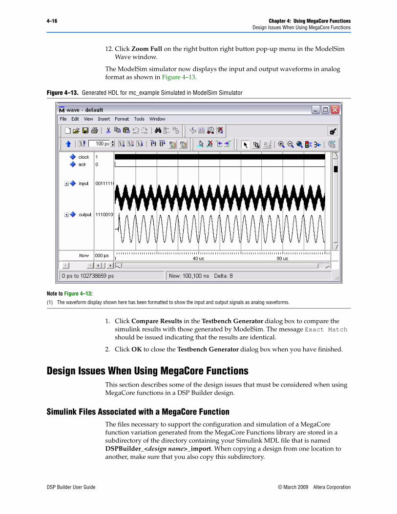
4–16 Chapter 4: Using MegaCore FunctionsDesign Issues When Using MegaCore Functions
DSP Builder User Guide © March 2009 Altera Corporation
12. Click Zoom Full on the right button right button pop-up menu in the ModelSim Wave window.
The ModelSim simulator now displays the input and output waveforms in analog format as shown in Figure 4–13.
1. Click Compare Results in the Testbench Generator dialog box to compare the simulink results with those generated by ModelSim. The message Exact Match should be issued indicating that the results are identical.
2. Click OK to close the Testbench Generator dialog box when you have finished.
Design Issues When Using MegaCore FunctionsThis section describes some of the design issues that must be considered when using MegaCore functions in a DSP Builder design.
Simulink Files Associated with a MegaCore FunctionThe files necessary to support the configuration and simulation of a MegaCore function variation generated from the MegaCore Functions library are stored in a subdirectory of the directory containing your Simulink MDL file that is named DSPBuilder_<design name>_import. When copying a design from one location to another, make sure that you also copy this subdirectory.
Figure 4–13. Generated HDL for mc_example Simulated in ModelSim Simulator
Note to Figure 4–13:
(1) The waveform display shown here has been formatted to show the input and output signals as analog waveforms.
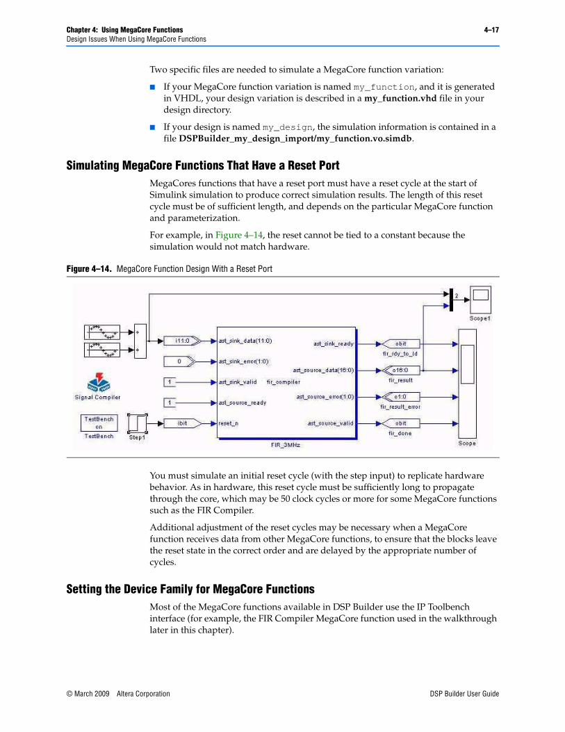
Chapter 4: Using MegaCore Functions 4–17Design Issues When Using MegaCore Functions
© March 2009 Altera Corporation DSP Builder User Guide
Two specific files are needed to simulate a MegaCore function variation:
■ If your MegaCore function variation is named my_function, and it is generated in VHDL, your design variation is described in a my_function.vhd file in your design directory.
■ If your design is named my_design, the simulation information is contained in a file DSPBuilder_my_design_import/my_function.vo.simdb.
Simulating MegaCore Functions That Have a Reset PortMegaCores functions that have a reset port must have a reset cycle at the start of Simulink simulation to produce correct simulation results. The length of this reset cycle must be of sufficient length, and depends on the particular MegaCore function and parameterization.
For example, in Figure 4–14, the reset cannot be tied to a constant because the simulation would not match hardware.
You must simulate an initial reset cycle (with the step input) to replicate hardware behavior. As in hardware, this reset cycle must be sufficiently long to propagate through the core, which may be 50 clock cycles or more for some MegaCore functions such as the FIR Compiler.
Additional adjustment of the reset cycles may be necessary when a MegaCore function receives data from other MegaCore functions, to ensure that the blocks leave the reset state in the correct order and are delayed by the appropriate number of cycles.
Setting the Device Family for MegaCore FunctionsMost of the MegaCore functions available in DSP Builder use the IP Toolbench interface (for example, the FIR Compiler MegaCore function used in the walkthrough later in this chapter).
Figure 4–14. MegaCore Function Design With a Reset Port

4–18 Chapter 4: Using MegaCore FunctionsDesign Issues When Using MegaCore Functions
DSP Builder User Guide © March 2009 Altera Corporation
The more recently introduced CIC MegaCore function uses an improved MegaWizard user interface. The interface for this MegaCore function always inherits the device family setting from the Signal Compiler block. If there is no Signal Compiler block in your design, the Stratix device family is chosen by default.
Older MegaCore functions (using the IP Toolbench user interface) allow you to modify the device family setting in the IP Toolbench interface.
The FFT, FIR Compiler, NCO, Reed Solomon Compiler, and Viterbi Compiler MegaCore functions have this behavior.
If you change the device family in Signal Compiler, you must check that any IP Toolbench MegaCore Functions have the correct device family set to ensure that the simulation models and generated hardware are consistent.
You can then run alt_dspbuilder_refresh_megacore as described in “Updating MegaCore Function Variation Blocks” on page 4–2 to ensure that all the MegaCore functions are up-to-date and consistent.

© March 2009 Altera Corporation DSP Builder User Guide
5. Using Hardware in the Loop (HIL)
IntroductionAdding the Hardware in the Loop (HIL) block to your Simulink model allows you to co-simulate a Quartus II software design with a physical FPGA board implementing a portion of that design. You define the contents and function of the FPGA by creating and compiling a Quartus II project. A simple JTAG interface between Simulink and the FPGA board links the two.
The main benefits of using the HIL block are faster simulation and richer instrumentation. The Quartus II project you embed in an FPGA runs faster than a software-only simulation. To further increase simulation speed, the HIL block offers frame and burst modes of data transfer that are significantly faster than single-step mode when used with suitable designs.
The HIL block also makes available to the hardware a large Simulink library of sinks and sources, such as channel models and spectrum analyzers, which can give you greater control and observability.
This chapter explains the HIL design flow, walks through an example using the HIL block, and discusses the optional burst and frame data transfer modes.
HIL Design FlowThe HIL block in AltLab library of the Altera DSP Builder Blockset enables the Hardware in the Loop functionality. It represents the functions implemented on your FPGA, and works smoothly with the normal DSP Builder/Simulink work flow.
The HIL design flow comprises the following steps:
1. Create a Quartus II project that defines the functions you want to co-simulate in hardware and use Signal Compiler block to compile the Quartus II project through the Quartus II Fitter.
2. Add the HIL block to your Simulink model and import the compiled Quartus II project into the HIL block. You can also connect instrumentation to your HIL block by adding additional blocks from the Simulink Sinks and Sources libraries.
1 If the original design contains a Clock block that defines a period and sample time that is different from the default values, you must add a Clock block with the same values to the HIL model.
3. Specify parameters for the HIL block, including the following options:
■ The Quartus II project you compiled to define its functionality
■ The clock and reset pins
■ The reset active level
■ The input and output pin characteristics
■ The use of single-step versus burst and frame mode

5–2 Chapter 5: Using Hardware in the Loop (HIL)HIL Requirements
DSP Builder User Guide © March 2009 Altera Corporation
4. Compile the HIL block to create a programming object file (.pof) for hardware co-simulation.
5. Scan for JTAG cables and hardware devices connected to the local host or any remotely enabled hosts.
6. Program the board that contains your target FPGA.
7. Simulate the combined software and hardware system in Simulink.
1 When using a HIL block in a Simulink model, set a fixed-step, single tasking solver. For information about setting the Simulink solver, refer to “Design Flow” on page 1–4.
Figure 5–1 shows this system-level design flow using DSP Builder.
HIL RequirementsYou need the following to use the HIL block:
■ An FPGA board with a JTAG interface (Stratix III, Stratix II, Stratix, Cyclone III, Cyclone II, or Cyclone device).
■ A valid Quartus II project that contains a single clock domain driven from Simulink. (An internal Quartus II project is created when you run Signal Compiler.)
■ A JTAG download cable (for example, a ByteBlasterMV™, ByteBlaster™ II, ByteBlaster, MasterBlaster™, or USB-Blaster™ cable).
■ A maximum of one HIL block for each JTAG download cable.
Figure 5–1. System-Level Design Flow

Chapter 5: Using Hardware in the Loop (HIL) 5–3HIL Walkthrough
© March 2009 Altera Corporation DSP Builder User Guide
HIL WalkthroughDSP Builder includes the following design examples in the <DSP Builder install path>\DesignExamples\Tutorials\HIL directory that demonstrate the use and effectiveness of HIL:
■ Imaging Edge Detection
■ Export Example
■ Fast Fourier Transform (FFT)
■ Frequency Sweep
This section walks through the Frequency Sweep design. It assumes you have completed Chapter 2, Getting Started Tutorial, and are familiar with using DSP Builder, MATLAB, Simulink, and the Quartus II software.
You also need an FPGA board connected to your computer with a JTAG download cable.
1 This walkthrough uses a Quartus II project which is created using DSP Builder and the Stratix II hardware device on an Altera Stratix II EP2S60 DSP Development Board. However, you could also use a Quartus II project created in the Quartus II software with any other supported device and board.
Perform the following steps:
1. Run MATLAB, and open the model FreqSweep.mdl in the <DSP Builder install path>\DesignExamples\Tutorials\HIL\FreqSweep directory. Figure 5–2 shows the loaded model.
2. Double-click the Signal Compiler block. In the dialog box that appears (Figure 5–3 on page 5–4), click Compile.
This action creates a Quartus II project, FreqSweep.qpf, compiles your model for synthesis, and runs the Quartus II Fitter.
Progress is indicated by status messages and a scrolling bar at the bottom of the dialog box.
Figure 5–2. Frequency Sweep Model

5–4 Chapter 5: Using Hardware in the Loop (HIL)HIL Walkthrough
DSP Builder User Guide © March 2009 Altera Corporation
3. Review the Messages, then click OK to close the Signal Compiler dialog box.
4. Replace the internal functions of the Frequency Sweep model with an HIL block. For this walkthrough, you can achieve this by opening the prepared model FreqSweep_HIL.mdl from the FreqSweep directory specified in Step 1.
Figure 5–4 shows this model, with the HIL block in place.
Figure 5–3. Signal Compiler Dialog Box, Simple Tab
Figure 5–4. Frequency Sweep Design Model Using the HIL Block

Chapter 5: Using Hardware in the Loop (HIL) 5–5HIL Walkthrough
© March 2009 Altera Corporation DSP Builder User Guide
5. Double-click the Frequency Sweep HIL block to display the Hardware in the loop dialog box (Figure 5–5).
6. Select the Quartus II project by browsing into the FreqSweep_dspbuilder directory to locate the FreqSweep.qpf file.
1 The full path to this file should be visible in the dialog box when this file is selected.
7. Select Clock from the list of available clock pins.
1 HIL does not support multiple clock domains and only the specifed signal is as the HIL clock signal. Any other clocks in your design are treated as input signals.
8. Select aclr from the list of available reset pins.
9. Identify the signed ports:
■ Select the input port and click Unsigned.
■ Select each output port (OutputCordic and OutputFilter) and click Signed.
Figure 5–5. Setting HIL Block Parameters, page 1 of 2

5–6 Chapter 5: Using Hardware in the Loop (HIL)HIL Walkthrough
DSP Builder User Guide © March 2009 Altera Corporation
10. Select the reset level to be Active_High.
11. Choose the mode of operation by turning off Burst Mode.
12. Click Next page. to display the second page of the Hardware in the loop dialog box (Figure 5–6).
13. Specify a value for the FPGA device and click Compile with Quartus II to compile the HIL design.
1 If no output is written to the MATLAB command window, check that the original Quartus II project is up-to-date and has been compiled by the same version of the Quartus II software as that used to compile your Simulink model.
14. Click Scan Jtag to find available cables and hardware devices in the chain.
15. Select the JTAG download cable that references the required FPGA device and click Configure FPGA to program the FPGA on the board.
16. Click Close.
Figure 5–6. Setting HIL Block Parameters, page 2 of 2

Chapter 5: Using Hardware in the Loop (HIL) 5–7Burst & Frame Modes
© March 2009 Altera Corporation DSP Builder User Guide
17. Simulate your design in Simulink. Figure 5–7 shows the scope display from the finished design.
Burst & Frame ModesThe Quartus II software infrastructure that communicates with the FPGA through JTAG—known as system-level debugging (SLD)—uses a serial data transfer protocol.
To maximize the throughput of this data transfer, the HIL block offers a burst mode that buffers the stimulus data and presents it in bursts to the hardware. Burst mode also allows a frame mode for certain types of designs.
Table 5–1 shows the advantages and disadvantages of using burst mode compared with the normal single-step mode.
Figure 5–7. Scope Output from the FrequencySweep Model with HIL Block
Table 5–1. Comparing Single-Step and Burst Modes
Single-Step Mode Burst Mode
Advantages Cycle accurate simulation.
Feedback is possible outside of the HIL block.
Low SLD overhead.
Fast HIL results.
Frame mode possible.
Disadvantages High SLD overhead.
No frame mode.
A latency is introduced on the output signals of the HIL block making feedback loop difficult outside the FPGA device.

5–8 Chapter 5: Using Hardware in the Loop (HIL)Burst & Frame Modes
DSP Builder User Guide © March 2009 Altera Corporation
Using Burst ModeYou can activate burst mode by turning on the Burst Mode option in the Hardware in the loop dialog box as shown in Figure 5–8.
When this option is set, you can specify the required number of data packets as the Burst length. The HIL block sends data to the hardware in bursts of the size you have specified.
1 The size of the packet is determined by the larger of the total input data width or the total output data width. If the packet size multiplied by the Burst length exceeds the preset data array, the Burst length is set to 1.
Simulation using burst mode works the same as single clock mode, but a latency of the specific packet size is introduced on the output signals of the HIL blocks. As a consequence, feedback-loops may not work properly unless they are enclosed in the HIL block, and some intervention may be necessary when comparing or visualizing HIL simulation results.
The HIL block uses software buffers to send and receive from the hardware, so you can change these buffer sizes without recompiling the HIL function.
Figure 5–8. Setting Parameters for the HIL Block in Figure 5–10
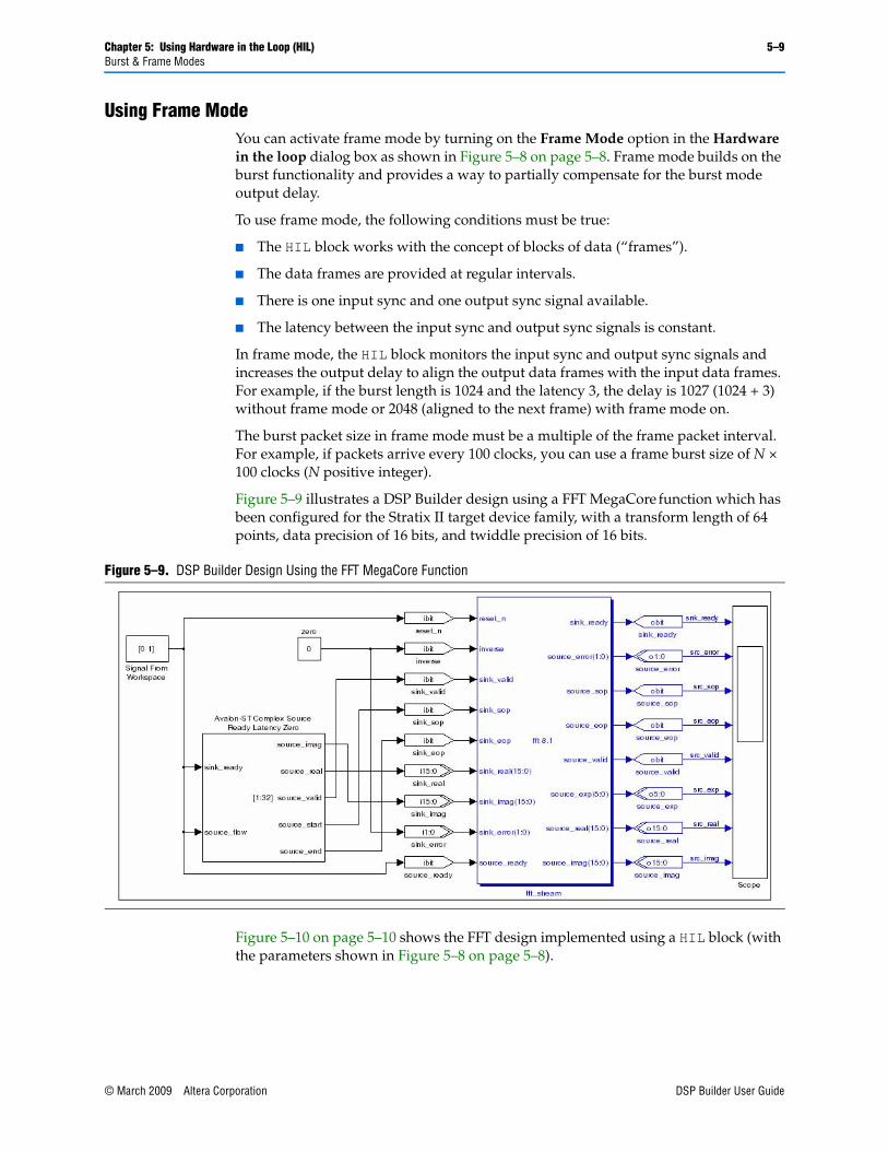
Chapter 5: Using Hardware in the Loop (HIL) 5–9Burst & Frame Modes
© March 2009 Altera Corporation DSP Builder User Guide
Using Frame ModeYou can activate frame mode by turning on the Frame Mode option in the Hardware in the loop dialog box as shown in Figure 5–8 on page 5–8. Frame mode builds on the burst functionality and provides a way to partially compensate for the burst mode output delay.
To use frame mode, the following conditions must be true:
■ The HIL block works with the concept of blocks of data (“frames”).
■ The data frames are provided at regular intervals.
■ There is one input sync and one output sync signal available.
■ The latency between the input sync and output sync signals is constant.
In frame mode, the HIL block monitors the input sync and output sync signals and increases the output delay to align the output data frames with the input data frames. For example, if the burst length is 1024 and the latency 3, the delay is 1027 (1024 + 3) without frame mode or 2048 (aligned to the next frame) with frame mode on.
The burst packet size in frame mode must be a multiple of the frame packet interval. For example, if packets arrive every 100 clocks, you can use a frame burst size of N × 100 clocks (N positive integer).
Figure 5–9 illustrates a DSP Builder design using a FFT MegaCore function which has been configured for the Stratix II target device family, with a transform length of 64 points, data precision of 16 bits, and twiddle precision of 16 bits.
Figure 5–10 on page 5–10 shows the FFT design implemented using a HIL block (with the parameters shown in Figure 5–8 on page 5–8).
Figure 5–9. DSP Builder Design Using the FFT MegaCore Function

5–10 Chapter 5: Using Hardware in the Loop (HIL)Troubleshooting HIL Designs
DSP Builder User Guide © March 2009 Altera Corporation
The Avalon-ST interface signals sink_eop and source_valid on the FFT MegaCore function are respectively used in the HIL block as the input sync and output sync.
f Refer to the FFT MegaCore Function User Guide for additional information on the input and output port signal timing.
Troubleshooting HIL DesignsThis section describes various issues that you may encounter when you are using HIL designs.
1 If the top-level of your design has changed, the Quartus II project must be compiled and reloaded into HIL to ensure that all information is up-to-date.
Failed to Load the Specified Quartus II ProjectHIL reads design information, such as clock, reset, and input and output ports, from the specified Quartus II project. However, it could fail to load your project if the project was not compiled through the Quartus II Fitter, there is a Quartus II version mismatch, or the Quartus II project file is not up-to-date.
Project Not Compiled Through the Quartus II FitterThis occurs when the specified Quartus II project has not been compiled successfully through the Quartus II Fitter.
Action:
Compile the project through the Quartus II Fitter before running HIL.
Figure 5–10. Using the FFT Design With an HIL Block

Chapter 5: Using Hardware in the Loop (HIL) 5–11Troubleshooting HIL Designs
© March 2009 Altera Corporation DSP Builder User Guide
Quartus II Version MismatchThis occurs when the specified Quartus II project is compiled using a different version of the Quartus II software than the one that is registered.
Action:
Compile the project using the registered Quartus II software before running HIL.
Quartus II Project File is Not Up-to-DateThis occurs when the specified Quartus II project file (.qpf) is older than your design model file. It is possible that your design model has changed or been saved after going through the Quartus II compilation process.
Action:
Recompile the specified the project again before running HIL.
No Inputs Found From the Quartus II ProjectThis could occur if the DSP Builder model file contains only the internally induced signals, such as from a counter, and also does not produce any outputs. However, HIL simulation works correctly.
Action:
None required.
No Outputs Found From the Quartus II ProjectThis could occur if your design does not have any outputs and makes the HIL simulation meaningless.
Action:
None required.
HIL Design Stays in Reset During SimulationAn asynchronous reset is permanently asserted for a HIL design.
Action:
Check that the reset active level matches the setting in the original design. Recompile the HIL design after you have changed the reset level.
HIL Compilation Appears to be HungAfter clicking Compile with Quartus II in the HIL Block Parameters dialog box, no output is written to the MATLAB command window. This can occur if the original Quartus II project was out-of-date or compiled by a different version of the Quartus II software.
Action:
Recompile the original project using the matching version of the Quartus II software.

5–12 Chapter 5: Using Hardware in the Loop (HIL)Troubleshooting HIL Designs
DSP Builder User Guide © March 2009 Altera Corporation
Scan JTAG Fails to Find Correct Cable or DeviceThis problem can occur if the target DSP board is connected and switched on after the HIL dialog box has been opened.
Action:
Close MATLAB. Reconnect the DSP board and switch on its power. In a command prompt window, type jtagconfig and verify that the correct JTAG cable and device is found. When you restart MATLAB, the Scan JTAG command should now find the correct cable and device.

© March 2009 Altera Corporation DSP Builder User Guide
6. Performing SignalTap II Logic Analysis
IntroductionThis chapter describes how to set up and run the SignalTap® II Embedded Logic Analyzer. In this walkthrough, you analyze three internal nodes in a simple switch controller design named switch_control.mdl. The design flow described in this example works for any of the Altera development boards that DSP Builder supports.
f For detailed information on the supported development boards, refer to the Boards Library chapter in the DSP Builder Reference Manual.
In this design, an LED on the DSP development board turns on or off depending on the state of user-controlled switches and the value of the incrementer. The design consists of an incrementer function feeding a comparator, and four switches fed into two AND gates. The comparator and AND gate outputs feed an OR gate, which feeds an LED on supported DSP development boards.
The SignalTap II Embedded Logic Analyzer captures the signal activity at the output of the two AND gates and the incrementer of the design loaded into the Altera device on DSP Builder-supported development boards. The logic analyzer retrieves the values and displays them in the MATLAB work space.
f For more information on using the SignalTap II Embedded Logic Analyzer with the Quartus II software, refer to the Quartus II Help or to Volume 3 of the Quartus II handbook.
You can instantiate a SignalTap II Logic Analyzer block in DSP Builder with the following characteristics:
■ Has a simple, easy-to-use interface
■ Analyzes signals in the top-level design file
■ Uses a single clock source
■ Captures data around a trigger point. 88% of the data is pre-trigger and 12% of the data is post-trigger
1 Alternatively, you can use the Quartus II software to instantiate of the SignalTap II Embedded Logic Analyzer in your design. The Quartus II software supports additional features, such as using multiple clock domains, and adjusting the percentage of data captured around the trigger point.
SignalTap II Design FlowWorking with the SignalTap II Embedded Logic Analyzer in DSP Builder involves the following flow:
1. Add a SignalTap II Logic Analyzer block to your design.
2. Specify the signals (nodes) that you want to analyze by inserting SignalTap II Node blocks.

6–2 Chapter 6: Performing SignalTap II Logic AnalysisIntroduction
DSP Builder User Guide © March 2009 Altera Corporation
3. Turn on the Enable SignalTap option in the Signal Compiler dialog box.
4. Choose one of the JTAG cable ports in the Signal Compiler dialog box or the SignalTap II Logic Analyzer dialog box.
5. Using Signal Compiler, synthesize your model, perform compilation in the Quartus II software, and download your design into the DSP development board (starter or professional).
6. Specify the required trigger conditions in the SignalTap II Logic Analyzer block.
f For details of the SignalTap II Logic Analyzer and SignalTap II Node blocks, refer to the descriptions of these blocks in the AltLab Library chapter of the DSP Builder Reference Manual.
SignalTap II NodesBy definition, a node represents a wire carrying a signal that travels between different logical components of a design file. The SignalTap II embedded logic analyzer can capture signals from any internal device node in a design file, including I/O pins.
The SignalTap II embedded logic analyzer can analyze up to 128 internal nodes or I/O elements. As more signals are captured, more logic elements (LEs) or embedded system blocks (ESBs) are used.
Before capturing signals, each node to be analyzed must be assigned to a SignalTap II embedded logic analyzer input channel. To assign a node to an input channel, you must connect it to a SignalTap II Node block.
SignalTap II Trigger ConditionsThe trigger pattern describes a logic event in terms of logic levels or edges. The SignalTap II Embedded Logic Analyzer uses a comparison register to recognize the moment when the input signals match the data specified in the trigger pattern.
The trigger pattern is composed of a logic condition for each input signal. By default, all signal conditions for the trigger pattern are set to “Don’t Care,” masking them from trigger recognition. You can select one of the following logic conditions for each input signal in the trigger pattern:
■ Don’t Care
■ Low
■ High
■ Rising Edge
■ Falling Edge
■ Either Edge
The SignalTap II embedded logic analyzer is triggered when it detects the trigger pattern on the input signals.

Chapter 6: Performing SignalTap II Logic Analysis 6–3SignalTap II Walkthrough
© March 2009 Altera Corporation DSP Builder User Guide
SignalTap II WalkthroughAltera provides several design files for this walkthrough in the directory structure shown in Figure 6–1.
You can start from the design in the original_design directory and go through the complete walkthrough.
Alternatively, you can use the design in the completed_walkthrough directory and go directly to “Turning On the SignalTap II Option in Signal Compiler” on page 6–7.
Opening the Walkthrough Example DesignOpen the template switch_control.mdl design in the <DSP Builder install path>\ DesignExamples\Tutorials\SignalTap\professional\original_design directory. (Figure 6–2).
Figure 6–1. SignalTap II Design Example Directory Structure
Figure 6–2. Starting Point for the SignalTap II Walkthrough

6–4 Chapter 6: Performing SignalTap II Logic AnalysisSignalTap II Walkthrough
DSP Builder User Guide © March 2009 Altera Corporation
Adding the Configuration and Connector BlocksYou must add the board configuration block and connector blocks for the board that you want to use. This walkthrough uses the Cyclone II EP2C35 development board.
1. Select the Boards library from the Altera DSP Builder Blockset folder in the Simulink library browser. Refer to the Getting Started Tutorial in Chapter 2 for instructions on accessing libraries.
2. Open the CycloneIIEP2C35 folder. Drag and drop the Cyclone II EP2C35 DSP Development Board configuration block into your model.
3. Drag and drop the SW2 and SW3 blocks close to the AND_Gate2 block in your model. Connect these switch blocks to the AND_Gate2 inputs.
4. Drag and drop the SW4 and SW5 blocks close to the AND_Gate1 block in your model. Connect these switch blocks to the AND_Gate1 inputs.
1 You can rotate the SW5 block to make the connection easier by right-clicking the block and clicking Rotate Block on the Format menu.
5. Drag and drop the LED0 block close to the OR_Gate block in your model. Connect this block to the OR_Gate output.
6. Select the Simulink Sources library. Drag and drop a Pulse Generator block near to the SW2 and SW3 blocks and connect it to these blocks.
7. Drag and drop another Pulse Generator block near the SW4 and SW5 blocks and connect it to these blocks.
Your model should look similar to Figure 6–3.
Figure 6–3. Switch Control Example with Board, Pulse Generator and Terminator Blocks

Chapter 6: Performing SignalTap II Logic Analysis 6–5SignalTap II Walkthrough
© March 2009 Altera Corporation DSP Builder User Guide
8. Use the Block Parameters dialog box to set the parameters shown in Table 6–1 for both pulse generator blocks (Figure 6–4).
9. Select the Simulink Sinks library. Drag and drop a Terminator block near to the OR_Gate block and connect it to this block.
Table 6–1. Parameters for the Pulse Generator Blocks
Parameter Value
Pulse type Time based
Time Use Simulation time
Amplitude 1
Period 2
Pulse Width 50
Phase delay 0
Interpret vector parameters as 1-D On
Figure 6–4. Pulse Generator Dialog Box

6–6 Chapter 6: Performing SignalTap II Logic AnalysisSignalTap II Walkthrough
DSP Builder User Guide © March 2009 Altera Corporation
Specifying the Nodes to AnalyzeIn the following steps, you add SignalTap II Node blocks to the signals (also called nodes) that you want to analyze; in this walkthrough they are the output of each AND gate and the output of the incrementer. Perform the following steps:
1. Open the AltLab library in the Simulink Library Browser. Drag a SignalTap II Node block into your design. Position the block so that it is on top of the connection line between the AND_Gate1 block and the OR_Gate block. Refer to Figure 6–5 if you are unsure of the positioning.
1 If you position the block using this method, the Simulink software inserts the block and joins connection lines on both sides.
2. Click the text under the block icon in your model and change the block instance name by deleting the text and typing the new text firstandout.
3. Add a SignalTap II Node block between the AND_Gate2 block and the OR_Gate block and name it secondandout.
4. Add a SignalTap II Node block between the Eightbit Counter block and the Comparator block and name it cntout.
5. Click Save on the File menu.
Figure 6–5. Completed SignalTap II Design

Chapter 6: Performing SignalTap II Logic Analysis 6–7SignalTap II Walkthrough
© March 2009 Altera Corporation DSP Builder User Guide
Turning On the SignalTap II Option in Signal CompilerWhen you add node blocks to signals, each block is implicitly connected to the SignalTap II embedded logic analyzer.
This is a functional change to your model and you must re-compile your design before you can use the SignalTap II embedded logic analyzer.
To compile your design, perform the following steps:
1. Double-click the Signal Compiler block and click the SignalTap II tab in the Signal Compiler dialog box (Figure 6–6).
2. Verify that the Enable SignalTap II option is on.
When this option is on, Signal Compiler inserts an instance of the SignalTap II embedded logic analyzer into your design.
3. Select a depth of 128 for the SignalTap II sample buffer (that is, the number of samples stored for each input signal) in the SignalTap II depth list.
4. Verify that the Use Base Clock option is on.
Figure 6–6. SignalTap II Tab in Signal Compiler

6–8 Chapter 6: Performing SignalTap II Logic AnalysisSignalTap II Walkthrough
DSP Builder User Guide © March 2009 Altera Corporation
5. Click the Simple tab and verify that the Use Board Block to Specify Device option is on (Figure 6–7).
6. Click the Compile button.
When the conversion is complete, information messages in the dialog box display the memory allocated during processing.
1 You must compile your design before you open the SignalTap II Analyzer block because the block relies on data files that are created during compilation.
7. Click Scan Jtag and select the appropriate download cable and device (for example, USB-Blaster cable and EP2C35 device).
8. Click Program to download your design to the development board.
9. Click OK.
Figure 6–7. Simple Tab in Signal Compiler

Chapter 6: Performing SignalTap II Logic Analysis 6–9SignalTap II Walkthrough
© March 2009 Altera Corporation DSP Builder User Guide
Specifying the Trigger LevelsTo specify the trigger levels, perform the following steps:
1. Double-click the SignalTap II Logic Analyzer block. The dialog box displays all the nodes connected to SignalTap II Node blocks as signals to be analyzed (Figure 6–8).
2. Specify the following trigger condition settings for the firstandout block:
a. Click firstandout under Signal Tap II Nodes.
b. Select Falling Edge in the Set Trigger Level list.
c. Click Change. The condition is updated.
3. Repeat these steps to specify the trigger condition High for the secondandout block.
The SignalTap II embedded logic analyzer captures data for analysis when it detects all trigger patterns simultaneously on the input signals. For example, because you specified Falling Edge for firstandout and High for secondandout, the SignalTap II embedded logic analyzer is only triggered when it detects a falling edge on firstandout and a logic level high on secondandout.
Figure 6–8. SignalTap II Logic Analyzer

6–10 Chapter 6: Performing SignalTap II Logic AnalysisSignalTap II Walkthrough
DSP Builder User Guide © March 2009 Altera Corporation
Performing SignalTap II AnalysisYou are now ready to run the analyzer and display the results in a MATLAB plot. After you click Acquire, the SignalTap II embedded logic analyzer begins analyzing the data and waits for the trigger conditions to occur.
Perform the following steps:
1. Click Scan Jtag in the SignalTap II Logic Analyzer dialog box and select the appropriate download cable and device.
2. Click Acquire.
3. Press switch SW4 on the DSP development board to trigger the SignalTap II embedded logic analyzer.
1 Note that if switch SW2 or SW 3 is pressed and held while pressing switch SW4, the trigger condition is not met and acquisition does not occur.
4. Click OK in the SignalTap II Logic Analyzer dialog box when you are finished.
The captured data are interpreted as unsigned values and displayed in MATLAB plots. The values are also stored in MATLAB .mat files in the working directory.
Figure 6–9 shows the MATLAB plot for the SignalTap II node firstandout.
Figure 6–10 shows the MATLAB plot for the SignalTap II node secondandout.
Figure 6–9. MATLAB Plot for SignalTap II Node firstandout
Figure 6–10. MATLAB Plot for SignalTap II Node secondandout

Chapter 6: Performing SignalTap II Logic Analysis 6–11SignalTap II Walkthrough
© March 2009 Altera Corporation DSP Builder User Guide
Figure 6–11 shows the MATLAB plot for the SignalTap II node cntout.
f For more information on the SignalTap II Logic Analyzer block, refer to the SignalTap II Logic Analyzer block description in the AltLab Library chapter in the DSP Builder Reference Manual.
Figure 6–11. MATLAB Plot for SignalTap II Node cntout

6–12 Chapter 6: Performing SignalTap II Logic AnalysisSignalTap II Walkthrough
DSP Builder User Guide © March 2009 Altera Corporation

© March 2009 Altera Corporation DSP Builder User Guide
7. Using the Interfaces Library
IntroductionThis chapter describes how to use the Avalon-MM blocks in the Interfaces library to create a design which functions as a custom peripheral to SOPC Builder.
SOPC Builder is a system development tool for creating systems that can contain processors, peripherals, and memories. SOPC Builder automates the task of integrating hardware components into a larger system.
To integrate a DSP Builder design into your SOPC Builder system, your peripheral must meet the Avalon-MM interface or Avalon-ST interface specification and qualify as a SOPC Builder-ready component.
The Interfaces library supports peripherals that use the Avalon-MM and Avalon-ST interface specifications.
1 The correct version of MATLAB with DSP Builder installed must be available on your system path to integrate DSP Builder MDL files in SOPC Builder.
Avalon-MM InterfaceThe Avalon Interface Specifications provide peripheral designers with a basis for describing the address-based read/write interface found on master (for example, a microprocessor or DMA controller) and slave peripherals (for example, a memory, UART, or timer).
The Avalon-MM Master and Avalon-MM Slave blocks in DSP Builder provide a seamless flow for creating a DSP Builder block as a custom peripheral and integrating the block into your SOPC Builder system. These blocks provide you the following benefits:
■ Automates the process of specifying Avalon-MM ports that are compatible with the Avalon-MM bus
■ Supports multiple Avalon-MM master and Avalon-MM slave instantiations
■ Saves time spent hand coding glue logic that connects Avalon-MM ports to DSP blocks
f For more information on SOPC Builder, refer to the Quartus II Handbook Volume 4: SOPC Builder. For more information on the Avalon-MM Interface, refer to the Avalon Interface Specifications.

7–2 Chapter 7: Using the Interfaces LibraryAvalon-MM Interface Blocks
DSP Builder User Guide © March 2009 Altera Corporation
Avalon-MM Interface BlocksA SOPC Builder component is a design module that SOPC Builder recognizes and can automatically integrate into a system.
SOPC Builder can recognize a DSP Builder design model provided that it is in the same working directory as the SOPC Builder project. With the Avalon-MM blocks provided in the DSP Builder library, you can design the DSP function and add an Avalon-MM block which makes it a custom peripheral in the Simulink environment.
Each Avalon-MM block can be instantiated multiple times in a design to implement an SOPC component with multiple master or slave ports.
Avalon-MM Slave BlockThe Avalon-MM Slave block supports the following signals:
■ clock
■ address
■ read
■ readdata
■ write
■ writedata
■ byteenable
■ readyfordata
■ dataavailable
■ endofpacket
■ readdatavalid
■ waitrequest
■ beginbursttransfer
■ burst count
■ irq
■ begintransfer
■ chipselect
f For more information about these signals, refer to the DSP Builder Reference Manual.

Chapter 7: Using the Interfaces Library 7–3Avalon-MM Interface Blocks
© March 2009 Altera Corporation DSP Builder User Guide
The block shown in Figure 7–1 describes an Avalon-MM slave interface where all the Avalon-MM signals have been enabled.
Figure 7–1. Avalon-MM Slave Block Signals

7–4 Chapter 7: Using the Interfaces LibraryAvalon-MM Interface Blocks
DSP Builder User Guide © March 2009 Altera Corporation
Each of the input and output ports of the block correspond to the input and output ports of the pin or bus shown between the ports.
Inputs to the DSP Builder core are displayed as right pointing bus/pins; outputs from the core are displayed as left pointing pins/buses.
You can use the opposite end of any pins to provide "pass-through" test data from the Simulink domain.
Avalon-MM Master BlockYou may want to use an Avalon-MM Master block (for example, to design a DMA controller) in a design which functions as an Avalon-MM Master in your SOPC Builder system.
The Avalon-MM Master block is similar to the Avalon-MM Slave block and supports the following signals:
■ clock
■ waitrequest
■ address
■ read
■ readdata
■ write
■ writedata
■ byteenable
■ endofpacket
■ readdatavalid
■ flush
■ burstcount
■ irq
■ irqnumber
f For more information about these signals, refer to the DSP Builder Reference Manual.
The block shown in Figure 7–2 on page 7–5 describes an Avalon-MM master interface where all the Avalon-MM signals have been enabled.

Chapter 7: Using the Interfaces Library 7–5Avalon-MM Interface Blocks
© March 2009 Altera Corporation DSP Builder User Guide
Wrapped BlocksWhile the Avalon-MM Master and Avalon-MM Slave interface blocks allow you to generate a SOPC Builder component in DSP Builder, they do little to mask the complexities of the interface. The Avalon-MM read and write FIFO blocks in the Interfaces library provide a higher level of abstraction.
You can implement a typical DSP core that handles data in a streaming manner, using the signals Data, Valid, and Ready. To provide a high level view, configurable Avalon-MM Write FIFO and Avalon-MM Read FIFO blocks are provided for you to map Avalon-MM interface signals to this protocol.
Figure 7–2. Avalon-MM Master Block Signals

7–6 Chapter 7: Using the Interfaces LibraryAvalon-MM Interface Blocks
DSP Builder User Guide © March 2009 Altera Corporation
Figure 7–3 shows an example system with Avalon-MM Write FIFO and Avalon-MM Read FIFO blocks.
Avalon-MM Write FIFOAn Avalon-MM Write FIFO has the following ports:
■ TestData (input): This port should be connected to a Simulink block that provides simulation data to the Avalon-MM Write FIFO. The data is passed to the DataOut port one cycle after the Ready input port is asserted.
■ Stall (input): This port should be connected to a Simulink block. It simulates stall conditions of the Avalon-MM bus and hence underflow to the SOPC Builder component. For any simulation cycle where Stall is asserted, the test data is cached by the Avalon-MM Write Test Converter and released in order, one sample per clock, when stall is de-asserted.
■ Ready (input): This port should be connected to a DSP Builder block. It indicates that the downstream hardware is ready for data.
■ DataOut (output): This port should be connected to a DSP Builder block and corresponds to the oldest unsent data sample received on the TestData port.
■ DataValid (output): This port should be connected to a DSP Builder block and is asserted whenever DataOut corresponds to real data.
Double-clicking on an Avalon-MM Write FIFO block opens the Block Parameters dialog box which you can use to set parameters for the data type, data width and FIFO depth.
Figure 7–3. Example System with Avalon-MM Write FIFO and Avalon-MM Read FIFO Blocks

Chapter 7: Using the Interfaces Library 7–7Avalon-MM Interface Blocks
© March 2009 Altera Corporation DSP Builder User Guide
Figure 7–4 shows the Avalon-MM Write FIFO dialog box.
f For more information about these signals, refer to the DSP Builder Reference Manual.
1 You can open the hierarchy below the Avalon-MM Write FIFO block by right-clicking the block and clicking Look Under Mask on the pop-up menu.
You can use this design as a template to design new functionality if required (for example, when you use an Avalon-MM address input to split incoming streams).
Figure 7–4. Figure 4: Avalon-MM Write FIFO Block Parameters

7–8 Chapter 7: Using the Interfaces LibraryAvalon-MM Interface Blocks
DSP Builder User Guide © March 2009 Altera Corporation
The internal content of an Avalon-MM Write FIFO is shown in Figure Figure 7–5.
The Avalon-MM Write Test Converter block handles caching and conversion of Simulink/MATLAB data into accesses over the Avalon-MM interface. You can use this block to test the functionality of your design. The Avalon-MM Write Test Converter is simulation only and does not synthesize to HDL.
Avalon-MM Read FIFOAn Avalon-MM Read FIFO has the following ports:
■ Stall (input): This port should be connected a Simulink block. It simulates stall conditions of the Avalon-MM bus and hence back pressure to the SOPC Builder component. For any simulation cycle where Stall is asserted, no Avalon-MM reads take place and the internal FIFO fills. When full, the Ready output is de-asserted so that no data is lost.
■ Data (input): This port should be connected to a DSP Builder block and should be connected to outgoing data from the user design.
■ DataValid (input): This port should be connected to a DSP Builder block and should be asserted whenever the signal on the Data port corresponds to real data.
■ TestDataOut (output): This port should be connected to a Simulink block and corresponds to data received over the Avalon-MM bus.
■ TestDataValid (output): This port should be connected to a Simulink block and is asserted whenever TestDataOut corresponds to real data.
■ Ready (output): When asserted, indicates that the block is ready to receive data.
Double-clicking on an Avalon-MM Write FIFO block opens the Block Parameters dialog box which you can use to set parameters for the data type, data width and FIFO depth.
f For more information about these signals, refer to the DSP Builder Reference Manual.
Figure 7–5. Avalon-MM Write FIFO Content

Chapter 7: Using the Interfaces Library 7–9Avalon-MM Interface Blocks Walkthrough
© March 2009 Altera Corporation DSP Builder User Guide
You can open the hierarchy below the Avalon-MM Read FIFO block by right-clicking on the block and choosing Look Under Mask from the pop-up menu.
The internal content of an Avalon-MM Read FIFO is shown in Figure 7–6.
The Avalon-MM Read Data Converter block handles caching and conversion of Simulink/MATLAB data into accesses over the Avalon-MM interface. You can use this block to test the functionality of your design. The Avalon-MM Read Data Converter is simulation only and does not synthesize to HDL.
Avalon-MM Interface Blocks WalkthroughThis walkthrough describes how to interface a design using the Avalon-MM Blocks as a custom peripheral to the Nios II embedded processor in SOPC Builder.
The design consists of a 4-tap FIR filter with variable coefficients. The coefficients are loaded using the Nios II embedded processor while the input data is supplied by an off-chip source through an analog-to-digital converter. The filtered output data is sent off-chip through a digital-to-analog converter.
Adding Avalon-MM Blocks to the Example DesignTo complete the example design, perform the following steps:
1. Click Open on the File menu in the MATLAB software.
2. Browse to the <DSP Builder install path>\DesignExamples\Tutorials\ SOPCBuilder\SOPCBlock directory.
Figure 7–6. Avalon-MM Read FIFO Content

7–10 Chapter 7: Using the Interfaces LibraryAvalon-MM Interface Blocks Walkthrough
DSP Builder User Guide © March 2009 Altera Corporation
3. Select the new_topavalon.mdl file and click Open.
Figure 7–7 shows new_topavalon.mdl.
4. Rename the file by clicking Save As on the File menu. Create a new folder called MySystem and save your new MDL file as topavalon.mdl in this folder.
5. Open the Simulink Library Browser by clicking on the icon or by typing simulink at the MATLAB command prompt.
6. Expand the Altera DSP Builder Blockset in the Simulink Library Browser and select Avalon Memory-Mapped in the Interfaces library.
7. Drag and drop an Avalon-MM Slave block into the top left of your model. Change the block name to Avalon_MM_Write_Slave.
8. Double-click on the Avalon_MM_Write_Slave block to bring up the Block Parameters dialog box.
9. Select Write for the address type, Signed Integer for the data type, and specify 8 bits for the data width. Turn off the Allow Byte Enable option (Figure 7–8 on page 7–11).
Figure 7–7. new_topavalon.mdl Example Design

Chapter 7: Using the Interfaces Library 7–11Avalon-MM Interface Blocks Walkthrough
© March 2009 Altera Corporation DSP Builder User Guide
10. Click OK.
Notice that the Avalon_MM_Write_Slave block is redrawn with three ports: Address i1:0, Write ibit, and Write Data i7:0.
Figure 7–8. Block Parameters for Avalon_MM_Write_Slave in topavalon.mdl

7–12 Chapter 7: Using the Interfaces LibraryAvalon-MM Interface Blocks Walkthrough
DSP Builder User Guide © March 2009 Altera Corporation
11. Connect the ports as shown in Figure 7–9.
1 Note that you can re-size a block by dragging the resize handles at each corner.
12. Drag and drop another Avalon-MM Slave block into the top right of your model and change the name of this block instance to Avalon_MM_Read_Slave.
13. Double-click on the Avalon_MM_Read_Slave block to bring up the Block Parameters dialog box.
14. Select Read for the address type, Signed Integer for the data type, and specify 8 bits for the data width.
15. Click OK and notice that the Avalon_MM_Read_Slave block is redrawn with three ports: Address i1:0, Read ibit, and Read Data o7:0.
16. Complete your design by connecting the Avalon_MM_Read_Slave ports as shown in Figure 7–9.
1 The default design example is configured to use the Stratix II EP2S60 DSP Development Board. If you have a different board (such as the Cyclone II EP2C35 Development Board, you must replace the board block and analog-to-digital converter blocks by corresponding blocks for the appropriate board. for more information, refer to the Boards Library chapter in the DSP Builder Reference Manual.
Figure 7–9. topavalon.mdl Example Design

Chapter 7: Using the Interfaces Library 7–13Avalon-MM Interface Blocks Walkthrough
© March 2009 Altera Corporation DSP Builder User Guide
17. Add oscilloscope probes to monitor the signals on the DSP development board.
18. Click Save on the File menu in your model window to save your model.
19. Run a simulation and observe the results on the oscilloscope probes. Coefficient values 1 0 0 0 should be loaded into the filter.
Verifying the DesignBefore using your design in SOPC Builder, you should use the TestBench block to verify your design.
Perform the following steps:
1. Double-click the TestBench block to display the TestBench Generator dialog box (Figure 7–10).
2. Click Compare against HDL.
Figure 7–10. TestBench Dialog Box

7–14 Chapter 7: Using the Interfaces LibraryAvalon-MM Interface Blocks Walkthrough
DSP Builder User Guide © March 2009 Altera Corporation
This process generates HDL, runs Simulink and ModelSim, and then compares the simulation results. Progress messages are issued in the dialog box which should complete with a message “Exact Match”.
3. Click OK.
Running Signal CompilerPerform the following steps to generate all the hardware and files required by the Quartus II software:
1. Double-click on the Signal Compiler block to display the Signal Compiler dialog box (Figure 7–11).
2. Verify that the Device is set to match your target development kit and click Compile.
3. When the compilation has completed successfully, click OK.
Figure 7–11. Signal Compiler Dialog Box

Chapter 7: Using the Interfaces Library 7–15Avalon-MM Interface Blocks Walkthrough
© March 2009 Altera Corporation DSP Builder User Guide
Instantiating the Design in SOPC BuilderTo instantiate your design as a custom peripheral to the Nios II embedded processor in SOPC Builder, perform the following steps:
1. Start the Quartus® II software.
2. On the File menu in the Quartus II software, click New Project Wizard.
a. Specify the working directory for your project by browsing to <DSP Builder install path>\DesignExamples\Tutorials\SOPCBuilder\SOPCBlock\ MySystem.
b. Specify a name for your project. This walkthrough uses SOPC for the project name.
1 The Quartus II software automatically specifies a top-level design entity that has the same name as the project. This walkthrough assumes that the names are the same.
c. Click Next in the New Project Wizard, until you get to the Family and Device Settings page. Verify that the selected device matches the FPGA on your DSP development board (if applicable).
d. Click Finish to create the Quartus II project.
3. On the Tools menu, click Tcl Scripts and perform the following steps:
a. Select topavalon_add.tcl in the Project folder.
b. Click Run to load your .mdl file and other required files into the Quartus II project.
4. On the Tools menu, click SOPC Builder and set the following parameters in the Create New System dialog box (Figure 7–12):
a. Specify SOPC as the system name.
b. Select VHDL for the target HDL.
c. Click OK.
Figure 7–12. SOPC Builder Create New System Dialog Box
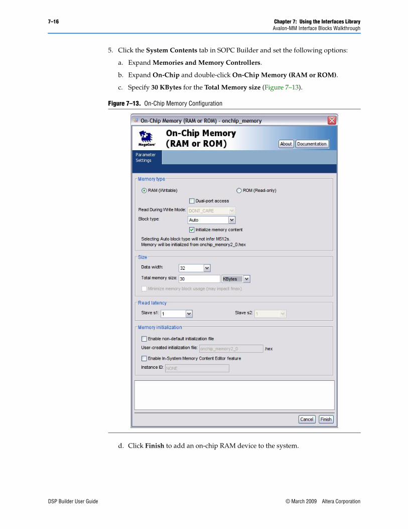
7–16 Chapter 7: Using the Interfaces LibraryAvalon-MM Interface Blocks Walkthrough
DSP Builder User Guide © March 2009 Altera Corporation
5. Click the System Contents tab in SOPC Builder and set the following options:
a. Expand Memories and Memory Controllers.
b. Expand On-Chip and double-click On-Chip Memory (RAM or ROM).
c. Specify 30 KBytes for the Total Memory size (Figure 7–13).
d. Click Finish to add an on-chip RAM device to the system.
Figure 7–13. On-Chip Memory Configuration
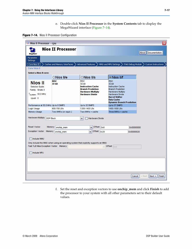
Chapter 7: Using the Interfaces Library 7–17Avalon-MM Interface Blocks Walkthrough
© March 2009 Altera Corporation DSP Builder User Guide
e. Double-click Nios II Processor in the System Contents tab to display the MegaWizard interface (Figure 7–14).
f. Set the reset and exception vectors to use onchip_mem and click Finish to add the processor to your system with all other parameters set to their default values.
Figure 7–14. Nios II Processor Configuration

7–18 Chapter 7: Using the Interfaces LibraryAvalon-MM Interface Blocks Walkthrough
DSP Builder User Guide © March 2009 Altera Corporation
g. Expand Peripherals and Debug and Performance. Double-click on System ID Peripheral and click Finish to accept the default settings.
h. Expand Interface Protocols and Serial. Double-click on JTAG UART and click Finish to accept the default settings.
i. Expand DSPBuilder Systems and double-click the topavalon_interface module to include it in your Nios II system (Figure 7–15).
1 If the memory device, Nios II processor, debug peripheral, interface protocol, and DSP Builder system are added in this order, you should not need to set a base address. However, you can click Auto-Assign Base Addresses on the System menu to automatically add a base address if necessary.
6. Click Generate to generate the SOPC Builder system. The sytem generation may take several minutes.
After the system generation in SOPC Builder has completed, you can design the rest of your Nios II embedded processor system using the standard Nios II embedded processor design flow. (Continue with this walkthrough to exercise the system from software using the Nios II processor.)
Figure 7–15. Including Your DSP Builder Design Module in SOPC Builder

Chapter 7: Using the Interfaces Library 7–19Avalon-MM Interface Blocks Walkthrough
© March 2009 Altera Corporation DSP Builder User Guide
Compiling the Quartus II ProjectTo compile the Quartus II project, perform the following steps:
1. On the Assignments menu in the Quartus II software, click Device to display the Device page of the Settings dialog box and create the basic pin settings as follows:
a. In the Settings dialog box, click Device and Pin Options.
b. In the Device and Pin Options dialog box, click the Unused Pins tab, select As input tri-stated and click OK.
c. Click OK to close the Settings dialog box.
2. On the Assignments menu, click Pins to open the Pin Planner and make pin assignments for clk and reset_n as shown in Table 7–1 (depending on which development board you are using).
1 If the Location column is not displayed, right-click in the pin assignments table and click Customize Columns to change the table display.
You can ignore all other pin assignments for this walkthrough.
3. Close the Pin Planner.
4. On the Processing menu, click Start Compilation to compile the Quartus II project.
5. When the compilation has completed, click Programmer on the Tools menu and click Start in the Quartus II Programmer to program the FPGA device on your development board.
6. Close the Quartus II Programmer window.
Testing the DSP Builder Block from SoftwareA C program is provided that loads a set of four coefficient into the filter, reads them back, and then repeats the process. To use this program, perform the following steps:
1. On the Nios II menu in SOPC Builder, click Nios II IDE.
2. Create a new Nios II C/C++ application as follows:
a. On the File menu in the Nios II IDE, point to New and click Project.
b. Nios II C/C++ Application.
c. In the New Project wizard, select Nios II C/C++ Application and click Next.
Table 7–1. Pin Assignments for the Stratix II and Cyclone II Development Boards
Node Name Direction Location
Stratix II EP2S60 or EP2S60ES DSP Development Board
clk Input PIN_AM17
reset_n Input PIN_AG19
Cyclone II EP2C35 DSP Development Board
clk Input PIN_N2
reset_n Input PIN_A14

7–20 Chapter 7: Using the Interfaces LibraryAvalon-MM Interface Blocks Walkthrough
DSP Builder User Guide © March 2009 Altera Corporation
d. Type test_DSP_Block for the Name of the project and select the Blank Project template (Figure 7–16).
e. Turn on Specify Location and browse to the directory <DSP Builder install path>\DesignExamples\Tutorials\SOPCBuilder\SOPCBlock\MySystem.
f. Click on Make a New Folder and create a software subdirectory.
g. Click OK.
h. Browse to the System PTF File <DSP Builder install path>\DesignExamples\ Tutorials\SOPCBuilder\SOPCBlock\MySystem\SOPC.ptf
i. Click Finish in the New Project wizard.
j. Verify that the application project test_DSP_Block appears in the Nios II C/C++ Projects list.
3. Add the test software to the new project as follows:
a. Locate the file test_DSP_Block.c in your file system. (<DSP Builder install path>\DesignExamples\Tutorials\SOPCBuilder\SOPCBlock\)
Figure 7–16. Nios II IDE New Project Wizard

Chapter 7: Using the Interfaces Library 7–21Avalon-MM Interface Blocks Walkthrough
© March 2009 Altera Corporation DSP Builder User Guide
b. Right-click on the test_DSP_Block.c file and click Copy.
c. Select the test_DSP_Block project folder in the Nios II IDE and paste the test_DSP_Block.c file into the project.
4. Set some of the reduced code footprint options in the Nios II IDE as follows:
a. Right-click on the Nios II IDE application project, test_DSP_Block, and click Properties.
b. In the Properties dialog box (Figure 7–17) click System Library.
c. Turn on Reduced device drivers and Small C library.
d. Turn off Support C++.
e. Click OK.
5. Run the test_DSP_Block software project in the Nios II IDE by right-clicking on test_DSP_Block and clicking Run As Nios II Hardware.
The project is compiled and the application code run on the development board. You should observe the following results in the Nios II IDE Console:
LOADING...
Coefficient 1 = 1
Coefficient 2 = 0
Coefficient 3 = 0
Coefficient 4 = 0
RELOADING...
Coefficient 1 = 0
Coefficient 2 = 0
Coefficient 3 = 1
Coefficient 4 = 0
f For information on using SOPC Builder to create a custom Nios II embedded processor, refer to AN 351: Simulating Nios II Embedded Processor Designs.
1 Completed versions of the topavalon.mdl design for the Cyclone II EP2C35 and Stratix II EP2S60 DSP development boards are available in the <DSP Builder install path>\DesignExamples\Tutorials\SOPCBuilder\SOPCBlock\Finished Examples directory.
Figure 7–17. Nios II IDE System Library Settings
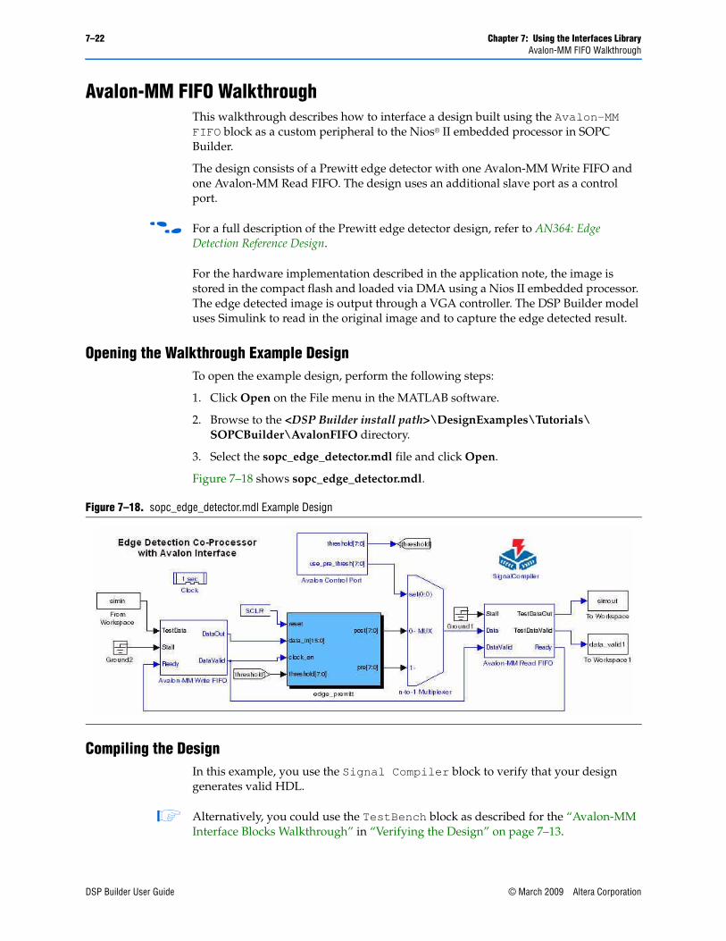
7–22 Chapter 7: Using the Interfaces LibraryAvalon-MM FIFO Walkthrough
DSP Builder User Guide © March 2009 Altera Corporation
Avalon-MM FIFO WalkthroughThis walkthrough describes how to interface a design built using the Avalon-MM FIFO block as a custom peripheral to the Nios® II embedded processor in SOPC Builder.
The design consists of a Prewitt edge detector with one Avalon-MM Write FIFO and one Avalon-MM Read FIFO. The design uses an additional slave port as a control port.
f For a full description of the Prewitt edge detector design, refer to AN364: Edge Detection Reference Design.
For the hardware implementation described in the application note, the image is stored in the compact flash and loaded via DMA using a Nios II embedded processor. The edge detected image is output through a VGA controller. The DSP Builder model uses Simulink to read in the original image and to capture the edge detected result.
Opening the Walkthrough Example DesignTo open the example design, perform the following steps:
1. Click Open on the File menu in the MATLAB software.
2. Browse to the <DSP Builder install path>\DesignExamples\Tutorials\ SOPCBuilder\AvalonFIFO directory.
3. Select the sopc_edge_detector.mdl file and click Open.
Figure 7–18 shows sopc_edge_detector.mdl.
Compiling the DesignIn this example, you use the Signal Compiler block to verify that your design generates valid HDL.
1 Alternatively, you could use the TestBench block as described for the “Avalon-MM Interface Blocks Walkthrough” in “Verifying the Design” on page 7–13.
Figure 7–18. sopc_edge_detector.mdl Example Design

Chapter 7: Using the Interfaces Library 7–23Avalon-MM FIFO Walkthrough
© March 2009 Altera Corporation DSP Builder User Guide
Perform the following steps to verify your design:
1. Double-click the Signal Compiler block.
2. Select the family and device for the DSP Development board you are using. The walkthrough design is configured for a Stratix 1S25 board (Figure 7–19).
3. Click Compile.
4. When the compilation has completed successfully, click OK.
1 The Avalon-MM Read/Write Converter is simulation only and does not synthesize to HDL.
Figure 7–19. Signal Compiler Dialog Box

7–24 Chapter 7: Using the Interfaces LibraryAvalon-MM FIFO Walkthrough
DSP Builder User Guide © March 2009 Altera Corporation
Instantiating the Design in SOPC BuilderTo instantiate your design as a custom peripheral to the Nios II embedded processor in SOPC Builder, perform the following steps:
1. Start the Quartus II software.
2. On the File menu in the Quartus II software, click New Project Wizard and set the following options:
a. Specify the working directory for your project by browsing to <DSP Builder install path>\DesignExamples\Tutorials\SOPCBuilder\AvalonFIFO.
b. Specify a name for your project. This walkthrough uses FIFO for the project name.
1 The Quartus II software automatically specifies a top-level design entity that has the same name as the project. This walkthrough assumes that the names are the same.
c. Click Finish to create the Quartus II project.
3. On the Tools menu, click Tcl Scripts and set the following options:
a. Load your design by selecting sopc_edge_detector_add.tcl in the Project folder.
b. Click Run.
4. On the Tools menu, click SOPC Builder to display the Create New System dialog box.
a. Specify AvalonFIFO as the system name.
b. Select VHDL for the target HDL.
c. Click OK.
5. Click the System Contents tab in SOPC Builder and set the following options:
a. Expand Memories and Memory Controllers.
b. Expand On-Chip and double-click On Chip Memory (RAM or ROM).
c. Click Finish to add an on-chip RAM device with default parameters.
6. Double-click the Nios II Processor module in the System Contents tab to display the MegaWizard interface.
7. Set the reset and exception vectors to use onchip_memory2_0 and click Finish to add the processor to your system with all other parameters set to their default values.
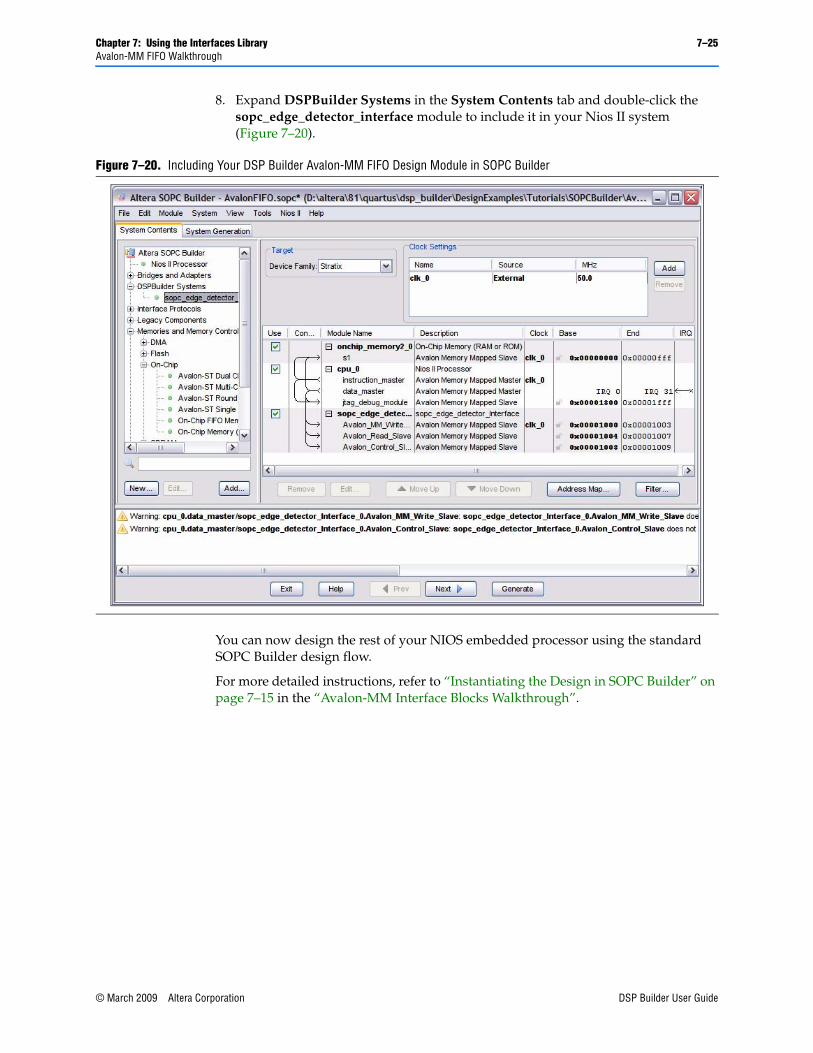
Chapter 7: Using the Interfaces Library 7–25Avalon-MM FIFO Walkthrough
© March 2009 Altera Corporation DSP Builder User Guide
8. Expand DSPBuilder Systems in the System Contents tab and double-click the sopc_edge_detector_interface module to include it in your Nios II system (Figure 7–20).
You can now design the rest of your NIOS embedded processor using the standard SOPC Builder design flow.
For more detailed instructions, refer to “Instantiating the Design in SOPC Builder” on page 7–15 in the “Avalon-MM Interface Blocks Walkthrough”.
Figure 7–20. Including Your DSP Builder Avalon-MM FIFO Design Module in SOPC Builder

7–26 Chapter 7: Using the Interfaces LibraryAvalon-ST Interface
DSP Builder User Guide © March 2009 Altera Corporation
Avalon-ST InterfaceAll DSP MegaCore functions in the DSP Builder MegaCore Functions library have interfaces that are compliant with the Avalon Interface Specifications. You can combine multiple MegaCore functions and easily because they use a common interface. This section summarizes the key features of the Avalon-ST interface.
The Avalon Interface Specifications define how to convey data between a source interface and a sink interface. The integrity of the data is indicated by a feed forward signal, valid. The specification also defines how the MegaCore functions may stall other blocks (backpressure) or regulate the rate at which data is provided by using a feedback sideband signal, ready.
You can configure the DSP Builder Avalon-ST Source and Avalon-ST Sink blocks with a ready latency of 0 or 1. The ready latency is the number of cycles that a source must wait after a sink has asserted ready so that a data transfer is possible. The source interface provides valid data at the earliest time possible, and it holds that data until ready is asserted by the sink. The ready signal notifies the source interface that the data has been sampled on that clock cycle.
For the ready_latency = 0 mode, Figure 7–21 shows the interaction that occurs between the source interface valid signal and the sink interface ready signal.
On cycle one, the source provides data and asserts valid even though the sink is not ready. The source waits until cycle two and the sink acknowledges that it has sampled the data by asserting ready. On cycle three, the source happens to provide data on the same cycle that the sink is ready to receive it and so the transfer occurs immediately. On the fourth cycle, the sink is ready but because the source has not provided any valid data, the data bus is not sampled.
A beat is defined as the transfer of one unit of data between a source and sink interface. This unit of data may consist of one or more symbols, so it can support modules that convey more than one piece of information on each valid cycle. This concept is useful because some modules have parallel input interfaces and other instances require serial input interfaces. For example, when conveying an in-phase and quadrature component on the same clock cycle. The choice depends on the algorithm, optimization technique, and throughput requirements.
Figure 7–21. Avalon-ST Interface Timing for ready-latency=0

Chapter 7: Using the Interfaces Library 7–27Avalon-ST Interface
© March 2009 Altera Corporation DSP Builder User Guide
Figure 7–22 gives an example of a data transfer where two symbols are conveyed on each beat - an in phase symbol I and a quadrature symbol Q. In this example, each symbol is eight bits wide.
The Avalon Interface Specifications also describe several mechanisms to support the transfer of data associated with multiple channels. Altera recommends that this is achieved using packet based transfers where each packet has a deterministic format and each channel is allocated a specific field (time slot in a packet).
Packet transfers require two additional signals that mark the start and the end of the packet. The MegaCore functions are designed with internal counters that count the samples in a packet so they know which channel a particular sample is associated with and synchronize appropriately with the start and end of packet signals. In Figure 7–22, the in phase and quadrature components associated with three different channels are conveyed between two MegaCore functions.
Avalon-ST Packet FormatsThe data associated with each channel can be allocated a field in a packet. To describe the relationship between the input and the output interfaces of a MegaCore function, you must define the packets associated with each interface.
The basic format of a packet is described using two parameters: SymbolsPerBeat, and PacketDescription. The SymbolsPerBeat parameter defines the number of symbols that are presented in parallel on every valid cycle. The PacketDescription is a string description of the fields in the packet.
A basic PacketDescription is a comma-separated list of field names, where a field name starts with a letter and may include the characters a-zA-Z0-9_. Typical field names include Channel1, Channel2, and Q. Field names are case sensitive and white space is not permitted.
Figure 7–22. Packetized Data Transfer

7–28 Chapter 7: Using the Interfaces LibraryAvalon-ST Interface
DSP Builder User Guide © March 2009 Altera Corporation
Figure 7–23 shows an example of a generic function that has two input interfaces and performs a transformation on the two input streams.
Avalon-ST Packet Format ConverterThe packet format converter (PFC) is a flexible, multipurpose component that transforms packets that are received from one function into a packet format that is supported by another function.
The PFC takes packet data from one or more input interfaces, and provides field reassignment in time and space to one or more output packet interfaces. You can specify the input packet format and the desired output packet format. The appropriate control logic is automatically generated.
Each input interface has Avalon-ST ready, valid, startofpacket, endofpacket, empty, and data signals. Each output interface has an additional error bit, which is asserted to indicate a frame delineation error.
The PFC performs data mapping on a packet by packet basis, so that there is exactly one input packet on each input interface for each output packet on each output interface. The packet rate of the converter is limited by the interface with the longest packet. When the PFC has multiple output interfaces, the packets on each output interface are aligned so that the startofpacket signal is presented on the same clock cycle.
If each interface supports fixed-length packets, the multi-packet mapping option can be selected, and the PFC can map fields from multiple input packets to multiple output packets.
f For a complete description of the Avalon-ST interface, refer to the Avalon Interface Specifications. For an example of a design that uses Avalon-ST interfaces and the Packet Format Converter blocks, refer to AN442: Tool Flow for Design of Digital IF for Wireless Systems.
Figure 7–23. Generic Function

© March 2009 Altera Corporation DSP Builder User Guide
8. Using Black Boxes for HDL Subsystems
IntroductionThe Signal Compiler block converts subsystems described using blocks from the DSP Builder block libraries into HDL code. Non-DSP Builder blocks, such as encapsulations of your own pre-existing HDL code, require the Signal Compiler block to recognize them as black boxes so that they are not altered by the conversion process.
There are two types of black box interface in DSP Builder: implicit and explicit.
Implicit Black Box InterfaceThe implicit black box interface can be inferred by using the HDL Import block.
The Signal Compiler block recognizes the HDL Import block as a black box and bypasses this block during the HDL translation.
f For information on the HDL Import block, refer to the block description in the AltLab Library chapter of the DSP Builder Reference Manual.
Explicit Black Box InterfaceThe explicit black box interface is specified using the HDL Input, HDL Output, HDL Entity, and Subsystem Builder blocks.
Using the HDL Input, HDL Output, and HDL Entity blocks prevents Signal Compiler from translating the subsystem into HDL. You can also use a Subsystem Builder block to create a new subsystem and then automatically populate its ports using the specified HDL.
You would typically use the explicit black box interface to encapsulate non-DSP Builder blocks from the main Simulink blocksets.
f For information on the HDL Input, HDL Output, HDL Entity, and Subsystem Builder blocks, refer to the block descriptions in the AltLab Library chapter of the DSP Builder Reference Manual.
HDL Import WalkthroughThe HDL Import block provides an interface to import a HDL module into your DSP Builder design.
1 Imported VHDL must be defined using std_logic_1164 types. If your design uses any other VHDL type definitions (such as arithmetic or numeric types), you should write a wrapper which converts them to std_logic or std_logic_vector.
The following sections show an example of importing an existing HDL design written in VHDL into the DSP Builder environment using the HDL Import block.

8–2 Chapter 8: Using Black Boxes for HDL SubsystemsHDL Import Walkthrough
DSP Builder User Guide © March 2009 Altera Corporation
Importing Existing HDL FilesTo import existing HDL files into a DSP Builder design, perform the following steps in the Simulink software:
1. In MATLAB, change the current directory setting to: <DSP Builder install path>\DesignExamples\Tutorials\BlackBox\HDLImport
2. On the File menu, click Open and select empty_MyFilter.mdl.
This design file has some of the peripheral blocks instantiated including the input/output ports and source blocks that provide appropriate stimulus for simulation. It is missing the main filter function which you can import as HDL.
3. Rename the file by clicking Save As on the File menu. Name your new MDL file MyFilter.mdl.
4. Open the Simulink Library Browser by clicking on the icon or by typing simulink at the MATLAB command prompt.
5. In the Simulink Library Browser, expand the Altera DSP Builder Blockset and select the AltLab library.
6. Drag and drop a HDL Import block into your model.
7. Double-click on the HDL Import block to bring up the DSP Builder HDL Import dialog box (Figure 8–2 on page 8–3).
8. In the HDL Import dialog box, enable the Import HDL radio button and click on the Add button to select the HDL input files.
9. From the VHDL Black Box File dialog box, select the files fir_vhdl.vhd, four_mult_add.vhd, and final_add.vhd, then click on Open.
10. Ensure that fir_vhdl is specified as the name of the top-level design entity. The fir_vhdl.vhd file describes the top level entity which implements an 8-tap low-pass FIR filter design.
Figure 8–1.
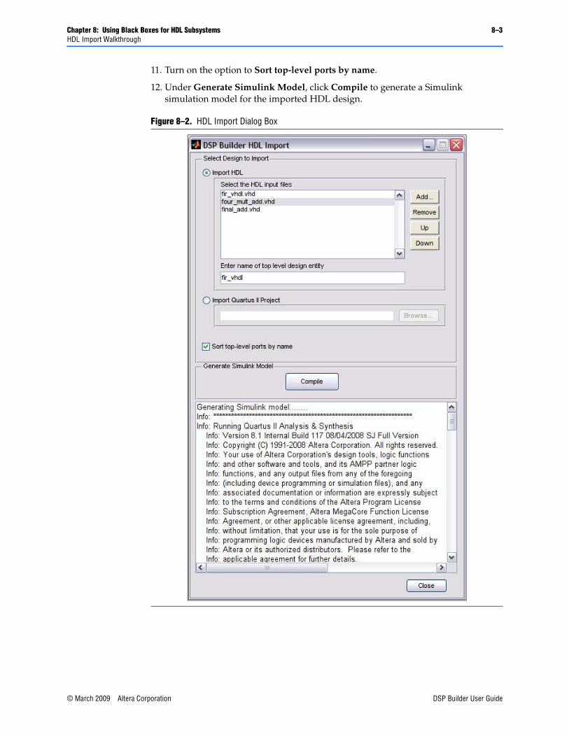
Chapter 8: Using Black Boxes for HDL Subsystems 8–3HDL Import Walkthrough
© March 2009 Altera Corporation DSP Builder User Guide
11. Turn on the option to Sort top-level ports by name.
12. Under Generate Simulink Model, click Compile to generate a Simulink simulation model for the imported HDL design.
Figure 8–2. HDL Import Dialog Box
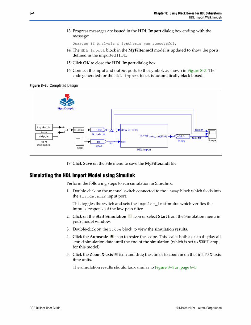
8–4 Chapter 8: Using Black Boxes for HDL SubsystemsHDL Import Walkthrough
DSP Builder User Guide © March 2009 Altera Corporation
13. Progress messages are issued in the HDL Import dialog box ending with the message:
Quartus II Analysis & Synthesis was successful.
14. The HDL Import block in the MyFilter.mdl model is updated to show the ports defined in the imported HDL.
15. Click OK to close the HDL Import dialog box.
16. Connect the input and output ports to the symbol, as shown in Figure 8–3. The code generated for the HDL Import block is automatically black boxed.
17. Click Save on the File menu to save the MyFilter.mdl file.
Simulating the HDL Import Model using SimulinkPerform the following steps to run simulation in Simulink:
1. Double-click on the manual switch connected to the Tsamp block which feeds into the fir_data_in input port.
This toggles the switch and sets the impulse_in stimulus which verifies the impulse response of the low-pass filter.
2. Click on the Start Simulation icon or select Start from the Simulation menu in your model window.
3. Double-click on the Scope block to view the simulation results.
4. Click the Autoscale icon to resize the scope. This scales both axes to display all stored simulation data until the end of the simulation (which is set to 500*Tsamp for this model).
5. Click the Zoom X-axis icon and drag the cursor to zoom in on the first 70 X-axis time units.
The simulation results should look similar to Figure 8–4 on page 8–5.
Figure 8–3. Completed Design

Chapter 8: Using Black Boxes for HDL Subsystems 8–5HDL Import Walkthrough
© March 2009 Altera Corporation DSP Builder User Guide
6. Double-click on the manual switch connected to the Tsamp block to select the chirp_in stimulus. (This is a sinusoidal signal whose frequency increases at a linear rate with time.)
7. Click on the Start Simulation icon or select Start from the Simulation menu in your model window.
8. Double-click on the Scope block to view the simulation results.
9. Press the Autoscale icon to resize the scope.
The simulation results should look similar to Figure 8–5.
This completes the HDL Import walkthrough. You can optionally compile your model for synthesis or perform RTL simulation on your design by following similar procedures to those described in the “Getting Started Tutorial”.
Figure 8–4. Simulink Simulation Results for the Impulse Stimulus
Figure 8–5. Simulink Simulation Results for the Chirp Stimulus
8–6 Chapter 8: Using Black Boxes for HDL SubsystemsSubsystem Builder Walkthrough
DSP Builder User Guide © March 2009 Altera Corporation
Subsystem Builder WalkthroughThe Subsystem Builder block makes it easy for you to import the input and output signals for a VHDL or Verilog HDL design into a Simulink subsystem.
If your HDL design contains any LPM or Megafunctions that are not supported by the HDL Import block, you should use the Subsystem Builder block. The Subsystem Builder block also allows you to create your own Simulink simulation model from non-DSP Builder blocks for faster simulation speed.
Unlike the HDL Import block described in the previous section, the Subsystem Builder block does not create a Simulink simulation model for the imported HDL design.
f For more information on the Subsystem Builder block, refer to the block description in the AltLab Library chapter in the DSP Builder Reference Manual.
In addition to porting the HDL design to a Simulink subsystem, you must create the Simulink simulation model for the block. The simulation models describes the functionality of the particular HDL subsystem. The following list shows the options available to create Simulink simulation models:
■ Simulink generic library
■ Simulink Blocksets (such as the DSP and Communications blocksets)
■ DSP Builder blockset
■ MATLAB functions
■ S-functions
1 You must add a Non-synthesizable Input block and a Non-synthesizable Output block around any DSP Builder blocks in the subsystem.
The following section shows an example which uses an S-function to describe the simulation models of the HDL code.
Creating a Black Box SystemTo create a black box system, perform the following steps:
1. In MATLAB, change the current directory to: <DSP Builder install path> \DesignExamples\Tutorials\BlackBox\SubSystemBuilder
2. Click Open on the File menu. Select the filter8tap.mdl file and click OK.
3. Open the Simulink Library Browser by clicking the Simulink icon or typing simulink at the MATLAB command prompt.
4. In the Simulink Library Browser, expand the AltLab library under the Altera DSP Builder blockset.
5. Drag a Subsystem Builder block into your model.

Chapter 8: Using Black Boxes for HDL Subsystems 8–7Subsystem Builder Walkthrough
© March 2009 Altera Corporation DSP Builder User Guide
6. Double-click the Subsystem Builder block.
The Subsystem Builder dialog box is displayed (Figure 8–6).
7. In the dialog box, browse for the fir_vhdl.vhd file and click Build.
This builds the subsystem and adds the signals for the fir_vhdl subsystem to the symbol in your filter8tap.mdl model. The Subsystem Builder dialog box is automatically closed.
8. Connect the ports as shown in Figure 8–7.
Figure 8–6. Subsystem Builder Dialog Box
Figure 8–7. filter8tap Design

8–8 Chapter 8: Using Black Boxes for HDL SubsystemsSubsystem Builder Walkthrough
DSP Builder User Guide © March 2009 Altera Corporation
9. Double-click on the fir_vhdl symbol. The filter8tap/fir_vhdl subsystem is opened (Figure 8–8).
The subsystem contains two HDL Input blocks (simulink_sclr and data_in) and a HDL Output block (data_out). Each of these blocks is in turn connected to a subsystem input or output. A HDL Entity block is also created to store the name of the HDL file and the names of the clock and reset ports.
1 The clock is handled implicitly and no port is explicitly created in the subsystem.
10. Leave your model window open for use in the next section.
In the next section, you build the simulation model that represents the functionality of this block in your Simulink simulations.
Building the Black Box SubSystem Simulation ModelFor this example, you use a S-function C++ simulation model to represent the 8-tap FIR filter block created in the previous section.
To create your model, perform the following steps:
1. In the Simulink Library Browser, expand the Simulink folder.
2. From the User-Defined Functions library, drag and drop a S-Function block into your model window.
3. Double-click the S-Function block to display the Function Block Parameters: S-Function dialog box (Figure 8–9 on page 8–9).
4. In the Block Parameters dialog box, change the S-Function name to Sfir8tap and enter the parameters -1 3962 4817 5420 5733 5733 5420 4817 3962.
The Sfir8tap function is a C++ Simulink S-Function simulation model written for the 8-tap Fir filter block.
The first parameter refers to the sampling rate (-1 indicates it inherits the sampling rate from the preceding block) and the rest of the parameters represent the eight filter coefficients.
1 The S-function modules parameter should be left with its default value.
Figure 8–8. Library: filter8tap/fir_vhdl Window

Chapter 8: Using Black Boxes for HDL Subsystems 8–9Subsystem Builder Walkthrough
© March 2009 Altera Corporation DSP Builder User Guide
5. Click the Edit button to view the code that describes the S-Function.
1 If the code does not appear automatically, click Browse and select the Sfir8tap.CPP file.
6. Scroll down in the Sfir8tap.CPP file to the S-function methods section.
The following code is an excerpt of the Simulink C++ S-Mex function code used to design a Simulink filter simulation model:
/*====================*
* S-function methods *
*====================*/
/* Function: mdlInitializeSizes=======================================
* Abstract:
* The sizes information is used by Simulink to determine the S-function
* block's characteristics (number of inputs, outputs, states, etc.).
*/
static void mdlInitializeSizes(SimStruct *S)
{
/* See sfuntmpl.doc for more details on the macros below */
ssSetNumSFcnParams(S, 9); /* Number of expected parameters */
if (ssGetNumSFcnParams(S) != ssGetSFcnParamsCount(S)) {
/* Return if number of expected != number of actual parameters */
return;
}// Set DialogParameters not tunable
const int iMaxssGetSFcnParamsCount = ssGetSFcnParamsCount(S);
Figure 8–9. Block Parameters: S-Function Dialog Box

8–10 Chapter 8: Using Black Boxes for HDL SubsystemsSubsystem Builder Walkthrough
DSP Builder User Guide © March 2009 Altera Corporation
for (int p=0;p<iMaxssGetSFcnParamsCount;p++)
{
ssSetSFcnParamTunable(S, p, 0);
}
if (!ssSetNumInputPorts(S, 1)) return;
ssSetInputPortWidth(S, 0, 1);
ssSetInputPortDataType(S, 0, SS_DOUBLE);
if (!ssSetNumOutputPorts(S, 1)) return;
ssSetOutputPortWidth(S, 0, 1);
ssSetOutputPortDataType(S, 0, SS_DOUBLE);
ssSetNumContStates(S, 0);
ssSetNumDiscStates(S, 1);
ssSetNumSampleTimes(S, 1);
ssSetNumRWork(S, 0);
ssSetNumIWork(S, 0);
ssSetNumDWork(S, DYNAMICALLY_SIZED); // reserve element in the
ssSetNumModes(S, 0); // pointers vector to store a C++ object
ssSetNumNonsampledZCs(S, 0);
ssSetOptions(S, 0);
}
During simulation, Simulink invokes certain callback methods from the S-function. The callback methods are sub-functions that initialize, update discrete states, and calculate output. The callback methods used in the example design are described in Table 8–1.
1. At the MATLAB command prompt, type:
mex Sfir8tap.CPP rThe mex command compiles and links the source file into a shared library executable in MATLAB called Sfir8tap.mexw32. (The extension is specific to 32-bit version of MATLAB run in Windows).
2. Close the editor window and click on OK to close the Function Block Parameters dialog box.
Table 8–1. Callback Methods Used in the S-Function
Callback Method Description
mdlInitializeSizes Specify the number of inputs, outputs, states, parameters, and other characteristics of the S-function.
mdlInitializeSampleTimes Specify the sample rates at which this S-function operates.
mdlStart Initialize the vectors of this S-function.
mdlOutputs Compute the signals that this block emits.
mdlUpdate Update the states of the block.
mdlTerminate Perform any actions required at termination of simulation.

Chapter 8: Using Black Boxes for HDL Subsystems 8–11Subsystem Builder Walkthrough
© March 2009 Altera Corporation DSP Builder User Guide
3. In the filter8tap/fir_vhdl window, connect the input port of the S-function block to the data_in block, and connect the output port of the S-function block to the data_out block as shown in Figure 8–10.
1 You do not need to connect the simulink_sclr block. The HDL Entity block automatically maps any input ports named simulink_clock in the VHDL entity to the global clock signal, and any input ports named simulink_sclr to the global synchronous clear signal.
4. Click Save on the File menu to save the filter8tap.mdl file.
Simulating the Subsystem Builder ModelPerform the following steps to run the Simulink simulation:
1. Click the Start Simulation icon or choose Start (Simulation menu) in the filter8tap.mdl window to begin the simulation.
2. Double-click the Scope block to view the simulation results. Click Autoscale to resize the scope.
3. Click the Zoom X-axis icon and use the cursor to zoom in on the first 22 x-axis time units.
The simulation results should appear similar to Figure 8–11.
1 Because the input is a pulse, the simulation results show the impulse response of the 8-tap FIR filter, which translates to the eight coefficient values. You can change the input stimulus to verify the step and random response of the filter.
Figure 8–10. S-Function Block Connection
Figure 8–11. Simulink Simulation Results of 8-Tap FIR Filter, Scope Window

8–12 Chapter 8: Using Black Boxes for HDL SubsystemsSubsystem Builder Walkthrough
DSP Builder User Guide © March 2009 Altera Corporation
Adding VHDL Dependencies to the Quartus II Project and ModelSimThe VHDL file used in this example is dependent on two other VHDL files. As specified, these two files are not examined by the Quartus II software or ModelSim, and compilation either fails or gives unexpected results. To resolve this, perform the following steps:
1. Double-click on the Signal Compiler block and click Compile. (Ignore the result for now.) This creates a directory called DSPBuilder_filter8tap_import in the directory containing your design.
1 Alternatively, you can create the directory DSPBuilder_filter8tap_import directly.
2. Copy the extra_add.tcl and extra_add_msim.tcl files from the original design directory to the DSPBuilder_filter8tap_import directory.
The extra_add.tcl file adds final_add.vhd and four_mult_add.vhd to the Quartus II project, while extra_add_msim.tcl compiles them in ModelSim when your design is run using the TestBench block. Any files ending with _add.tcl are executed by the Quartus II software when the project is created. Files ending with _add_msim.tcl are executed by ModelSim when it compiles your design testbench.
Simulate the Design in ModelSimPerform the following steps to test the simulation model against the HDL in ModelSim:
1. In the Simulink Library Browser, expand AltLab library under Altera DSP Builder Blockset.
2. Drag a TestBench block into your model.
3. Double-click on the TestBench block and click Compare against HDL (Figure 8–12 on page 8–13).
When the comparison has completed successfully an Exact Match message is issued in the TestBench Generator dialog box.
1 If you want to use ModelSim directly, click on the Advanced tab, turn on the Launch GUI option, and then click Run ModelSim.
This completes the Subsystem Builder walkthrough. You can optionally compile your model for synthesis by following similar procedures to those described in the “Getting Started Tutorial”.

Chapter 8: Using Black Boxes for HDL Subsystems 8–13Subsystem Builder Walkthrough
© March 2009 Altera Corporation DSP Builder User Guide
Figure 8–12. Testbench Generator Dialog Box for the filter8tap Design

8–14 Chapter 8: Using Black Boxes for HDL SubsystemsSubsystem Builder Walkthrough
DSP Builder User Guide © March 2009 Altera Corporation

© March 2009 Altera Corporation DSP Builder User Guide
9. Using Custom Library Blocks
IntroductionA parameterizable custom library block is a Simulink subsystem in which the block functionality is described using DSP Builder primitives. This design flow also supports parameterizable hierarchical subsystem structures.
An example of a custom library block is provided at <DSP Builder install path>\ DesignExamples\Tutorials\BuildingCustomLibrary\top.mdl. (Figure 9–1).
The RamBasedDelay block used in top.mdl, is an example of a custom parameterizable Simulink block and is defined in the library file MyLib.mdl. The RamBasedDelay block has one parameter, Delay.
Creating a Custom Library BlockTo create your own custom block, you perform the following steps:
1. Creating a Library Model File
2. Building the HDL Subsystem Functionality
3. Defining Parameters Using the Mask Editor
4. Linking the Mask Parameters to the Block Parameters
5. Making the Library Block Read Only
6. Adding the Library to the Simulink Library Browser
Figure 9–1. top.mdl Example

9–2 Chapter 9: Using Custom Library BlocksCreating a Custom Library Block
DSP Builder User Guide © March 2009 Altera Corporation
Creating a Library Model FileCreate a Library Model File for your custom block by performing the following steps in the Simulink software:
1. In MATLAB, change the current directory setting to: <DSP Builder install path>\DesignExamples\Tutorials\BuildingCustomLibrary.
2. Open the Simulink Library Browser by clicking the Simulink icon or typing simulink at the MATLAB command prompt.
3. On the File menu in the Simulink Library Browser, point to New and click Library to open a new library model window.
4. Expand the Simulink Ports & Subsystems library in the Simulink Library Browser and drag a Subsystem block into your model.
5. Click on the Subsystem text below the block and rename the block DelayFIFO.
1 You should always rename a block representing an HDL Subsystem to ensure that all the generated entities in a hierarchical design are unique.
6. Click Save on the File menu and save the library file as NewLib.mdl.
Building the HDL Subsystem FunctionalityTo add functionality to the DelayFIFO block, perform the following steps:
1. Double-click on the DelayFIFO block to open the NewLib/DelayFIFO subsystem window.
2. Drag and drop a Shift Taps block from the Storage library in the Altera DSP Builder Blockset into your model window. Insert the Shift Taps block between the input and output blocks (Figure 9–2).
3. Double-click the Shift Taps block to open the Block Parameters dialog box (Figure 9–3 and Figure 9–4 on page 9–3). Set the parameters shown in Table 9–1.
Figure 9–2. Shift Taps Block
Table 9–1. Parameters for the Shift Taps Block (Part 1 of 2)
Parameter Value
Main Tab
Number Of Taps 1
Distance Between Taps 10
Optional Ports and Settings Tab
Use Shift Out Port Off

Chapter 9: Using Custom Library Blocks 9–3Creating a Custom Library Block
© March 2009 Altera Corporation DSP Builder User Guide
Use Enable port: On
Use Dedicated Circuitry On
Memory Block Type Auto
Figure 9–3. Shift Taps Block Parameters
Figure 9–4. Shift Taps Block Optional Parameters
Table 9–1. Parameters for the Shift Taps Block (Part 2 of 2)
Parameter Value

9–4 Chapter 9: Using Custom Library BlocksCreating a Custom Library Block
DSP Builder User Guide © March 2009 Altera Corporation
4. Click OK to close the Block Parameters dialog box.
5. Add an Input block (In2) from the Simulink Ports & Subsystems library and connect it to the ena port on the Shift Taps block.
6. Rename the blocks as shown in Table 9–2.
7. Click Save on the File menu.
Figure 9–5 shows the completed DelayFIFO subsystem.
Figure 9–6 shows the NewLib library model which now shows the input and output ports defined in the DelayFIFO subsystem.
Defining Parameters Using the Mask EditorCreate parameters for the DelayFIFO block using the Mask Editor by performing the following steps:
1. Right-click the DelayFIFO block in the NewLib model and click Mask Subsystem on the pop-up menu.
2. In the Mask Editor dialog box (Figure 9–7 on page 9–5, Figure 9–8 on page 9–6, and Figure 9–9 on page 9–6), set the options shown in Table 9–3 on page 9–5.
Table 9–2. Renaming the Blocks
Old Name New Name
In1 InDin
In2 InEna
Shift Taps DRB
Out1 OutDout
Figure 9–5. DelayFIFO Subsystem
Figure 9–6. NewLib Model

Chapter 9: Using Custom Library Blocks 9–5Creating a Custom Library Block
© March 2009 Altera Corporation DSP Builder User Guide
Table 9–3. Parameters for the Mask Editor
Parameter Value
Icon Tab
Frame Visible
Transparency Opaque
Rotation Fixed
Units Autoscale
Drawing Commands port_label('input',1,'din');port_label('input',2,'ena');port_label('output',1,'dout');fprintf('Delay %d',d)
Parameters Tab (Note 1)
Prompt Delay
Variable d
Documentation Tab
Mask type SubSystem AlteraBlockSet
Mask description RAM-Based Delay ElementAltera Corporation
Note to Table 9–3:
(1) To add a parameter in the Parameters tab, click the button.
Figure 9–7. Mask Editor Icon Tab

9–6 Chapter 9: Using Custom Library BlocksCreating a Custom Library Block
DSP Builder User Guide © March 2009 Altera Corporation
3. Click OK in the Mask Editor dialog box.
4. Double-click on the DelayFIFO block in your NewLib model to display the Block Parameters dialog box.
5. Specify a Delay of 5 (Figure 9–10 on page 9–7).
Figure 9–8. Mask Editor Parameters Tab
Figure 9–9. Documentation Tab

Chapter 9: Using Custom Library Blocks 9–7Creating a Custom Library Block
© March 2009 Altera Corporation DSP Builder User Guide
6. Click OK in the Block Parameters dialog box.
7. Click Save on the File menu to save your library model.
f For more information on the Mask Editor, refer to the MATLAB Help.
Linking the Mask Parameters to the Block ParametersTo pass parameters from the symbol’s mask into the block, you use a model workspace variable.
1. Double-click the DRB block in the NewLib/DelayFIFO window to open the Block Parameters dialog box.
2. Copy the mask parameter variable name d from the Parameters tab of the Mask Editor into the Distance Between Taps field in the Block Parameters dialog box. (Figure 9–11)
Figure 9–10. Delay FIFO Block Parameters
Figure 9–11. Shift Taps Block Parameters

9–8 Chapter 9: Using Custom Library BlocksCreating a Custom Library Block
DSP Builder User Guide © March 2009 Altera Corporation
3. Click OK to close the Shift Taps Block Parameters dialog box.
4. Close your model window.
Making the Library Block Read OnlyA library block should be made read only so that it is not accidentally edited in a design model. To set the read/write permissions, perform the following steps:
1. Right-click the DelayFIFO block in the NewLib model and click SubSystem Parameters on the pop-up menu to display the Block Parameters dialog box.
2. In the Read/Write permissions list, select ReadOnly as shown in Figure 9–12.
1 The ReadWrite option would allow edits from both the library and the design. The NoReadOrWrite option would not allow Signal Compiler to generate HDL for the design. If you want to modify a library model, open your model, click Unlock Library on the File menu and change the read/write permissions in the Block Parameters dialog box. Remember to reset ReadOnly after changing the library model. Your changes are automatically propagated to all instances in your design.
3. Click OK to close the Block Parameters dialog box.
4. Click Save on the File menu to save your library model.
Adding the Library to the Simulink Library BrowserYou can add a custom library to the Simulink library browser by creating a file called slblocks.m. This file must be in the same location as your library file and both files must be in search path for MATLAB. To create this file, perform the following steps:
1. On the File menu in MATLAB, point to New and click M-File to open a new editor window.
Figure 9–12. Delay FIFO Block Parameters

Chapter 9: Using Custom Library Blocks 9–9Synchronizing a Custom Library
© March 2009 Altera Corporation DSP Builder User Guide
2. Enter the following text in the editor window:
function blkStruct = slblocks
blkStruct.Name = ['Custom Library DSP Builder'];blkStruct.OpenFcn = 'NewLib';blkStruct.MaskDisplay = '';% Define the Browser structure array, the first% element contains the information for the Simulink% block library and the second for the Simulink% Extras block library.Browser(1).Library = 'NewLib';Browser(1).Name = 'Custom Library DSP Builder';Browser(1).IsFlat = 0;blkStruct.Browser = Browser;
% End of slblocks
3. Save the M-file with the file name slblocks.m in the same directory as NewLib.mdl. The next time that you display the Simulink library browser the Custom Library should be available as shown Figure 9–13.
You can drag and drop a block from your custom library in the same way as from any other library in the Simulink library browser.
You can create a custom library with multiple blocks by creating the required blocks in the same library file.
f For more information about M-files, refer to the MATLAB Help. A template slblocks.m file with explanatory comments can be found at <MATLAB install path>\toolbox\ simulink\blocks\slblocks.m.
Synchronizing a Custom LibraryA custom library can contain MegaCore functions, HDL import, or state machine editor blocks. If your design is copied or moved, it may be necessary to synchronize your model containing these blocks by using the following command:
alt_dspbuilder_refresh_user_library_blocks
Figure 9–13. Custom Library in the Simulink Library Browser

9–10 Chapter 9: Using Custom Library BlocksSynchronizing a Custom Library
DSP Builder User Guide © March 2009 Altera Corporation
1 This command is automatically called when you use either of the commands:
alt_dspbuilder_refresh_hdlimport
or
alt_dspbuilder_refresh_megacore

© March 2009 Altera Corporation DSP Builder User Guide
10. Adding a Board Library
IntroductionThis chapter describes how to create and build a custom board library to use inside DSP Builder using built-in board components.
Each board library is defined by a XML board description file. This board description file contains all the board components and their FPGA pin assignments.
The following development boards are already supported in DSP Builder:
■ Cyclone II DE2 Starter board
■ Cyclone II EP2C35 board
■ Cyclone II EP2C70 board
■ Cyclone III EP3C25 Starter board
■ Cyclone III EP3C120 board
■ Stratix EP1S25 board
■ Stratix EP1S80 board
■ Stratix II EP2S60 board
■ Stratix II EP2S180 board
■ Stratix II EP2SGX90 PCI Express board
■ Stratix III EP3SL150 board
f For information about these boards, refer to the DSP Builder Reference Manual .
Creating a New Board DescriptionAdditional boards can be added by creating new board description files. You only need to create a board description file for each new board and run a MATLAB command to build it into DSP Builder Library.
You can use the existing components or create your own custom components.
Predefined ComponentsPredefined components can be found in the following folder:
<install dir>\quartus\dsp_builder\lib\boardsupport\components
There is a single XML file that describes each separate board component named <component_name>.component. This file defines its data type, direction, bus width, and appearance. The file also contains a brief description of the component.
Component TypesThere are three main types of component: Single Bit, Fixed Size Bus, and Selectable Single Bit.

10–2 Chapter 10: Adding a Board LibraryCreating a New Board Description
DSP Builder User Guide © March 2009 Altera Corporation
Single Bit Type:
These components have a single bit with one FPGA pin assigned to each component. The components are either inputs or outputs and cannot be changed. Predefined components of this type include:
■ Red and Green LEDs (LED0 to LED17 and LEDG0 to LEDG8)
■ Software switches (SW0 to SW17)
■ User push buttons (PB0 to PB3)
■ Reset push buttons (IO_DEV_CLRn and USER_RESETN)
■ RS232 receive output and RS232 transmit input pins (RS232Rout and RS232Tin)
Fixed-Size Bus Type:
These components have a fixed-sized group of same type (either Input or Output) pins with one FPGA pin assigned to each bit of the bus. Predefined components of this type include:
■ 12-bit analog-to-digital converter (A2D1Bit12 and A2D2Bit12)
■ 14-bit analog-to-digital converter (A2D1Bit14 and A2D2Bit14)
■ 14-bit digital-to-analog converter (D2A1 and D2A2)
■ 8-bit dual in-line package switch (DipSwitch)
■ 7-Segment display with a decimal point (SevenSegmentDisplay0 to SevenSegmentDisplay1)
■ Simple 7-Segment display without a decimal point (Simple7SegmentDisplay0 to Simple7SegmentDisplay7)
Selectable Single Bit Type:
These components have a single bit, but the pin can be selected from a group of predefined FPGA pins. Furthermore, the pin can be set as either input or output. Predefined components of this type include:
■ Debug pins (DebugA and DebugB)
■ Prototyping pins (PROTO, PROTO1 to PROTO3)
■ Evaluation input pin (EvalIoIn)
■ Evaluation output pin (EvalIoOut)
Component Description FileYou can define a new component by creating a corresponding component file named <component_name>.component in the same folder as the predefined components.
The component description file contains a root element component which contains several attributes and sub-elements that define the component. The component attributes are defined as follows:
■ displayname= Specifies the name of the component, which is referenced by the board description file.

Chapter 10: Adding a Board Library 10–3Creating a New Board Description
© March 2009 Altera Corporation DSP Builder User Guide
■ direction= Specifies the direction of the signal. It can have the value of Input or Output. You can omit this attribute for the Selectable Single Bit Type, because it is set later.
■ type= Specifies the data type of the signal. The type can be BIT, INT, or UINT. followed by the size in square brackets. For example, "BIT[1,0]" defines a single bit while "UINT[12,0]" is a 12-bit unsigned integer.
The component sub-elements are defined as follows:
■ <documentation> text </documentation> This sub-element contains text describing the component and one of the following variable that define how the pin name, or list of pin-names appears in the new board library:
■ %pinname% for Single Bit Type
■ %pinlist% for Selectable Single Bit Type
■ %indexedpinliat% for Fixed Size Bus Type
■ <display [attributes]> This sub-element has the attributes:
■ icon= Specifies the image file name for the component
■ width= Specifies the display width for the image file
■ height= Specifies the display height for the image file
1 For components without an image, you can omit the icon attribute and define a visual representation using the plot and fprintf commands. For example:
<display width="90" height="26">
plot([0 19 20 21 22 21 20 19], [0 0 1 0 0 0 -1 0]);
fprintf('EVAL IO OUT \n%pinname% ');
</display>
Example Component Description File:<component displayname="EVAL IO OUT" direction="Output"
type="BIT[1,0]">
<documentation>
Prototyping Area Pin Single Bit Output
%pinlist%
</documentation>
<display width="90" height="26">
plot([0 19 20 21 22 21 20 19],[0 0 1 0 0 0 -1 0]);
fprintf('EVAL IO OUT \n%pinname% ');
</display>
</component>

10–4 Chapter 10: Adding a Board LibraryCreating a New Board Description
DSP Builder User Guide © March 2009 Altera Corporation
Board Description FileThe board description file is named <board_name>.board and should be created in the folder:
<install dir>\quartus\dsp_builder\lib\boardsupport\boards
The board description file is divided into Header and Board Description sections.
Header SectionThis section contains a line that defines the XML version and character encoding used in the document:
<?xml version="1.0" encoding="UTF-8"?>
In this case, the document conforms to the 1.0 specification of XML and uses the ISO-8859-1 (Latin-1/West European) character set.
You should not modify this line.
Board Description SectionThe main body of the document is a root element board that has several attributes and sub-elements which define the details of the board.
<board Attributes>
<displayname> Text </displayname>
<component Attributes />
...........
<component Attributes />
<configuration Attributes>
<devices> Attributes>
</devices>
<option Attributes>
</option>
</configuration>
</board>
1 The last line in the file must be a closing tag for the root element board </board>.
The board attributes are defined as follows:
■ uniquename= A unique name used to reference the board.
■ family= Device family of the FPGA on board (assuming only one device is on the board).
The board must contain a displayname sub-element containing text that describes the board. For example:
<displayname>Cyclone II XYZ Board</displayname>

Chapter 10: Adding a Board Library 10–5Creating a New Board Description
© March 2009 Altera Corporation DSP Builder User Guide
This is followed by component sub-elements that declare the components:
■ Single bit type examples:
<component name="LED0" pin="Pin_E5"/>
<component name="LED1" pin="Pin_B3"/>
where attribute name defines the name of the component on the board and pin defines the FPGA pin to which the component is connected. The name must match one of the predefined components and can be used only once per board.
■ Fixed-size bus type example:
<component name="DipSwitch" label="S1">
<pin location="Pin_AC13"/> <!-- LSB -->
<pin location="Pin_A19"/>
<pin location="Pin_C21"/>
<pin location="Pin_C23"/>
<pin location="Pin_AE18"/>
<pin location="Pin_AE19"/> <!-- MSB-->
</component>
where attribute name defines the name of the component on the board and label defines the name of the component as it appears in Simulink. For a component with width n, there must be n pin sub-elements. The pin location must be a valid FPGA pin name. Note that the pin ordering is listed from LSB to MSB, with LSB on top of the list.
■ Selectable single bit type example:
<component name="PROTO1">
<pin location="Pin_C3"/>
<pin location="Pin_D2"/>
<pin location="Pin_L3"/>
<pin location="Pin_J7"/>
<pin location="Pin_J6"/>
<pin location="Pin_K6"/>
</component>
This element has the same format as the fixed-size bus type, but each pin element can be chosen from a specified list of available FPGA pin locations.
The configuration element defines the board configuration block. For example:
<configuration icon="dspboard2c35.bmp" width="166" height="144">
<devices jtag-code="0x020B40DD">
<device name="EP2C35F672C6" />
</devices>
<!-- Input clock selection list -->
<option name="ClockPinIn" label="Clock Pin In">
<pin location="Pin_N2"/>
<pin location="Pin_N25"/>

10–6 Chapter 10: Adding a Board LibraryBuilding the Board Library
DSP Builder User Guide © March 2009 Altera Corporation
<pin location="Pin_AE14"/>
<pin location="Pin_AF14"/>
<pin location="None"/>
</option>
<!-- Global Reset Pin -->
<option name="GlobalResetPin" label="Global Reset Pin">
<pin location="Pin_A14"/>
<pin location="Pin_AC18"/>
<pin location="Pin_AE16"/>
<pin location="Pin_AE22"/>
<pin location="None"/>
</option>
</configuration>
The configuration attributes are defined as follows:
■ icon = The image file to be used for the board configuration block
■ width = The width of the image
■ height = The height of the image
The devices sub-element has the following attributes:
■ jtag-code = The JTAG code of the FPGA device
■ device name = The device name of the FPGA used on the board
Each option sub-element has the following attributes:
■ name = The name of the option (clock or reset pin)
■ label = Labels that identifies the pins on the blocks
■ pin location = A list of selectable clock or reset pins
f For more examples, refer to any of the existing board description files.
Building the Board LibraryRestart MATLAB without opening the Simulink library and run the following command in the MATLAB command window to create the new board library:
alt_dspbuilder_createComponentLibrary

© March 2009 Altera Corporation DSP Builder User Guide
11. Using the State Machine Library
IntroductionThis chapter describes the design flow used to implement a state machine in DSP Builder.
Separate procedures are provided for “Using the State Machine Table Block” on page 11–2 and “Using the State Machine Editor Block” on page 11–8.
1 The State Machine Table block is not available on Linux and is deprecated on Windows. The State Machine Editor block should be used in new designs.
The example design, fifo_control_logic.mdl, contains a simple state machine used to implement the control logic for a first-in first-out (FIFO) memory structure.
The design files for this example are installed in the <DSP Builder install path>\ DesignExamples\Tutorials\StateMachine\StateMachineTable directory.
Figure 11–1 shows the top-level schematic for the FIFO design example.
The state machine in this design example feeds the control inputs of a Dual-Port RAM block and the inputs of an address counter.
Figure 11–1. FIFO Design Example Top-Level Schematic

11–2 Chapter 11: Using the State Machine LibraryUsing the State Machine Table Block
DSP Builder User Guide © March 2009 Altera Corporation
The operation of the state machine is as follows:
■ When the push input is asserted and the address counter is less than 250, the address counter is incremented and a byte of data is written to memory.
■ When the pop input is asserted and the address counter is greater than 0, the address counter is decremented and a byte of data is read from memory.
■ When the address counter is equal to 0, the empty flag is asserted.
■ When the address counter is equal to 250, the full flag is asserted.
Using the State Machine Table BlockThe following steps show how you can use the State Machine Table block to create the FIFO controller in the example design:
1. Add a State Machine Table block to your Simulink design and assign it a new name. Figure 11–2 shows the default State Machine Table block. In this example, the block is named fifo_controller.
1 You must save you model and change the default name of the State Machine Table block before you define the state machine properties.
2. Double-click the fifo_controller block to define the state machine properties.
The State Machine Builder dialog box appears with the Inputs tab selected. The Inputs tab displays the input names defined for your state machine and provides an interface to allow you to add, and delete input names.
3. Delete the default input names In2, In3, In4, and In5 and enter the following new input names:
■ count_in
■ pop
■ push
1 You can add or delete inputs but you cannot change an existing input name directly. You cannot delete or change the reset input.
Figure 11–2. fifo_controller State Machine Table Block

Chapter 11: Using the State Machine Library 11–3Using the State Machine Table Block
© March 2009 Altera Corporation DSP Builder User Guide
Figure 11–3 shows the Inputs tab after the inputs have been defined for the FIFO design example.
4. Click the States tab.
The States tab displays the state names defined for your state machine and provides an interface to allow you to add, change, and delete state names. The States tab also allows you to select the reset state for your state machine. The reset state is the state to which the state machine transitions when the reset input is asserted.
1 You must define at least two states for the state machine. You cannot delete or change the name of a state while it is selected as the reset state.
5. Use the Add, Change, and Delete buttons to replace the default states S1, S2, S3, S4, and S5 with the following states:
■ empty (reset state)
■ full
■ idle
■ pop_not_empty
■ push_not_full
Figure 11–4 on page 11–4 shows the State Machine Builder States tab after the states have been edited for the FIFO design example.
Figure 11–3. State Machine Builder Inputs Tab

11–4 Chapter 11: Using the State Machine LibraryUsing the State Machine Table Block
DSP Builder User Guide © March 2009 Altera Corporation
6. After specifying the input and state names, click the Conditional Statements tab and use it to describe the behavior of your state machine by adding the statements shown in Table 11–1.
Figure 11–4. State Machine Builder States Tab
Table 11–1. FIFO Controller Conditional Statements
Current State Condition Next State
empty (push=1)&(count_in!=250) push_not_full
empty (push=0)&(pop=0) idle
full (push=0)&(pop=0) idle
full (pop=1) pop_not_empty
idle (pop=1)&(count_in=0) empty
idle (push=1) push_not_full
idle (pop=1)&(count_in!=0) pop_not_empty
idle (push=1)&(count_in=250) full
pop_not_empty (push=0)&(pop=0) idle
pop_not_empty (pop=1)&(count_in=0) empty
pop_not_empty (push=1)&(count_in!=250) push_not_full
pop_not_empty (pop=1)&(count_in!=0) pop_not_empty
pop_not_empty (push=1)&(count_in=250) full
push_not_full (push=0)&(pop=0) idle
push_not_full (pop=1)&(count_in=0) empty
push_not_full (push=1)&(count_in!=250) push_not_full
push_not_full (push=1)&(count_in=250) full
push_not_full (pop=1)&(count_in!=0) pop_not_empty

Chapter 11: Using the State Machine Library 11–5Using the State Machine Table Block
© March 2009 Altera Corporation DSP Builder User Guide
The Conditional Statements tab displays the state transition table, which contains the conditional statements that define your state machine.
1 There must be at least one conditional statement defined in the Conditional Statements tab.
A conditional statement consists of a current state, a condition that causes a transition to take place, and the next state to which the state machine transitions. The current state and next state values must be state names defined in the States tab and can be selected from a list in the dialog box.
1 To indicate in a conditional statement that a state machine always transitions from the current state to the next state, specify the conditional expression to be one.
Figure 11–5 shows the Conditional Statements tab, after defining the conditional statements for the FIFO controller.
When a state machine is in a particular state, it may need to evaluate more than one condition to determine the next state to which it transitions. The priority of the conditional operator determines the priority if the condition contain only one operator.
Figure 11–5. State Machine Builder Conditional Statements Tab

11–6 Chapter 11: Using the State Machine LibraryUsing the State Machine Table Block
DSP Builder User Guide © March 2009 Altera Corporation
Table 11–2 shows the conditional operators you can use to define a conditional expression.
If the conditions contain multiple operators, they are evaluated in the order that you list them in the conditional statements table.
Table 11–3 shows the conditional statements when the current state is idle.
The condition (pop=1)&(count_in=0) is higher in the table than the condition (push=1)&(count_in=250), therefore it has higher priority.
The condition (pop=1)&(count_in!=0) has the next highest priority and the condition (push=1)&(count_in=250) has the lowest priority.
7. Use the Move Up and Move Down buttons to change the order of the conditional statements, as shown in Table 11–4.
Table 11–2. Comparison Operators Supported in Conditional Expressions
Operator Description Priority Example
- (unary) Negative 1 -1
(...) Brackets 1 (1)
= Numeric equality 2 in1=5
!= Not equal to 2 in1!=5
> Greater than 2 in1>in2
>= Greater than or equal to 2 in1>=in2
< Less than 2 in1<in2
<= Less than or equal to 2 in1<=in2
& AND 2 (in1=in2)&(in3>=4)
| OR 2 (in1=in2)|(in1>in2)
Table 11–3. Idle State Condition Priority
Current State Condition Next State
idle (pop=1)&(count_in=0) empty
idle push=1 push_not_full
idle (pop=1)&(count_in!=0) pop_not_empty
idle (push=1)&(count_in=250) full
Table 11–4. Idle State Condition Priority (Reordered)
Current State Condition Next State
idle (pop=1)&(count_in=0) empty
idle (push=1)&(count_in=250) full
idle (pop=1)&(count_in!=0) pop_not_empty
idle push=1 push_not_full

Chapter 11: Using the State Machine Library 11–7Using the State Machine Table Block
© March 2009 Altera Corporation DSP Builder User Guide
8. Click the Design Rule Check tab. You can use this tab to verify that the state machine you defined in the previous steps does not violate any of the design rules. Click Analyze to evaluate the design rules for your state machine. If a design rule is violated, an error message, highlighted in red, is listed in the Analysis Results box. If error messages appear in the analysis results, fix the errors and re-run the analysis until no error messages appear before simulating and generating VHDL for your design. Figure 11–6 shows the Design Rule Check tab after clicking Analyze.
9. To save the changes made to your state machine, click OK.
The State Machine Builder dialog box closes and returns you to your Simulink design file. The design file is automatically updated with the input and output names defined in the previous steps.
1 You may need to resize the block to ensure that the input and state names do not overlap and are displayed correctly.
Figure 11–7 shows the updated fifo_controller block.
Figure 11–6. State Machine Builder Design Rule Check Tab
Figure 11–7. fifo_controller Block After Closing the State Machine Table

11–8 Chapter 11: Using the State Machine LibraryUsing the State Machine Editor Block
DSP Builder User Guide © March 2009 Altera Corporation
Using the State Machine Editor BlockThe following steps show how you can use the State Machine Editor block to create the FIFO controller in the example design:
1. Add a State Machine Editor block to your Simulink design and assign it a new name. Figure 11–8 shows the default State Machine Editor block. In this example, the block is named fifo_controller.
1 You should save you model and change the default name of the State Machine Editor block before you define the state machine properties.
2. Double-click the fifo_controller block to open the State Machine Editor in the Quartus II software (Figure 11–9).
3. On the Tools menu in the Quartus II State Machine Editor, point to State Machine Wizard and click Create a new state machine design.
Figure 11–8. fifo_controller State Machine Editor Block
Figure 11–9. Quartus II State Machine Editor Window

Chapter 11: Using the State Machine Library 11–9Using the State Machine Editor Block
© March 2009 Altera Corporation DSP Builder User Guide
4. The first page of the wizard allows you to choose the reset mode, whether the reset is active-high or active-low, and whether the outputs are registered. Accept the default values (synchronous, active-high, registered outputs) and click Next to display the Transitions page of the wizard.
5. Delete the default state names (state1, state2, state3) and type the following new state names:
■ empty
■ full
■ idle
■ pop_not_empty
■ push_not_full
6. Delete the default input port names (input1, input2) and type the following new input port names:
■ count_in[7:0]
■ pop
■ push
1 Do not change the clock and reset port names. The count_in port must be defined as an 8-bit vector to allow count values up to 250.
7. Edit the state transitions by entering the statements shown in Table 11–1.
Table 11–5. FIFO Controller Transitions
Source State Destination State Condition
empty push_not_full (push==1)&(count_in!=250)
empty idle (push==0)&(pop==0)
full idle (push==0)&(pop==0)
full pop_not_empty (pop==1)
idle empty (pop==1)&(count_in==0)
idle push_not_full (push==1)
idle pop_not_empty (pop==1)&(count_in!=0)
idle full (push==1)&(count_in==250)
pop_not_empty idle (push==0)&(pop==0)
pop_not_empty empty (pop==1)&(count_in==0)
pop_not_empty push_not_full (push==1)&(count_in!=250)
pop_not_empty pop_not_empty (pop==1)&(count_in!=0)
pop_not_empty full (push==1)&(count_in==250)
push_not_full idle (push==0)&(pop==0)
push_not_full empty (pop==1)&(count_in==0)
push_not_full push_not_full (push==1)&(count_in!=250)
push_not_full full (push==1)&(count_in==250)
push_not_full pop_not_empty (pop==1)&(count_in!=0)

11–10 Chapter 11: Using the State Machine LibraryUsing the State Machine Editor Block
DSP Builder User Guide © March 2009 Altera Corporation
1 The transitions are validated on entry and must conform with Verilog HDL syntax.
Figure 11–10 shows the Transitions page after the states, inputs, and transitions have been defined.
8. Click Next to display the Actions page. Delete the default output port name (output1) and enter the following new output port names:
■ out_empty
■ out_full
■ out_idle
■ out_pop_not_empty
■ out_push_not_full
Figure 11–10. State Machine Editor Wizard Transitions Page

Chapter 11: Using the State Machine Library 11–11Using the State Machine Editor Block
© March 2009 Altera Corporation DSP Builder User Guide
9. Specify the output logic for each output port by specifying the action conditions to set each output port to 1 when the state is true and 0 for all other states as shown in Table 11–6.
Table 11–6. FIFO Controller Output Actions
Output Port Output Value In State
out_empty 1 empty
out_full 1 full
out_idle 1 idle
out_pop_not_empty 1 pop_not_empty
out_push_not_full 1 push_not_full
out_empty 0 full
out_empty 0 idle
out_empty 0 pop_not_empty
out_empty 0 push_not_full
out_full 0 empty
out_full 0 idle
out_full 0 pop_not_empty
out_full 0 push_not_full
out_idle 0 empty
out_idle 0 full
out_idle 0 pop_not_empty
out_idle 0 push_not_full
out_pop_not_empty 0 empty
out_pop_not_empty 0 full
out_pop_not_empty 0 idle
out_pop_not_empty 0 push_not_full
out_push_not_full 0 empty
out_push_not_full 0 full
out_push_not_full 0 idle
out_push_not_full 0 pop_not_empty

11–12 Chapter 11: Using the State Machine LibraryUsing the State Machine Editor Block
DSP Builder User Guide © March 2009 Altera Corporation
Figure 11–11 shows the Actions page after the output ports, and action conditions have been defined.
10. Click Next to display the Summary page. Check that the summary lists the five states (empty, full, idle, pop_not_empty, and push_not_full), the five input ports (clock, count_in[7:0], pop, push, and reset), and the five output ports (out_empty, out_full, out_idle, out_pop_not_full, and out_push_not_full).
11. Click Finish to complete the state machine definition. The state machine is displayed graphically in the State Editor window and should look similar to Figure 11–12 on page 11–13.
Figure 11–11. State Machine Editor Wizard Actions Page

Chapter 11: Using the State Machine Library 11–13Using the State Machine Editor Block
© March 2009 Altera Corporation DSP Builder User Guide
1 The first state that you entered in the wizard is marked as the default state. This should be the empty state and is the state to which the state machine transitions when the reset input is asserted.
12. On the Tools menu in the Quartus II State Machine Editor, click Generate HDL File to display the Generate HDL File dialog box. Select VHDL and click OK to confirm your choice. Click Yes to save the fifo_controller.smf file and check that there are no FSM verification errors.
1 There should be five warning messages stating that FSM verification is skipped in each state. These messages can be ignored.
If there are any errors, you can edit the state machine using the Properties dialog boxes that can be displayed from the right button pop-up menu when a state or transition is selected. You can also edit the state machine in table format by clicking the tabs at the bottom of the State Machine Editor window.
f For information about editing state machine properties and drawing a graphical state machine, refer to the About the State Machine Editor topic in the Quartus II Help that is available from the Help menu in the editor window.
13. On the File menu in the Quartus II State Machine Editor, click Exit.
The fifo_controller block on your model is updated with the input and output ports defined in the state machine.
Figure 11–12. Graphical fifo_controller State Machine Diagram

11–14 Chapter 11: Using the State Machine LibraryUsing the State Machine Editor Block
DSP Builder User Guide © March 2009 Altera Corporation
1 You may need to resize the block to ensure that the input and state names do not overlap and are displayed correctly.
Figure 11–13 shows the updated fifo_controller block for the FIFO design example.
Figure 11–13. fifo_controller Block After Closing the State Machine Editor

© March 2009 Altera Corporation DSP Builder User Guide
A. Managing Projects and Files
The following files are required to store all the components of a DSP Builder design:
■ The top level Simulink model <top_level_name>.mdl
■ The import directory DSPBuilder_<top_level_name>_import and its contents.
■ Any source files for imported HDL.
■ Any memory initialization (.hex) files.
■ Any referenced custom library files.
■ The analyzed Simulink model file <top_level_name>.mdlxml.
1 When the .mdlxml file is included in a Quartus II, MATLAB does not need to be called to synthesize the design. A project without the .mdlxml can still be synthesized, but must call MATLAB as part of the generation flow. If you do not want Quartus II synthesis to call MATLAB, or are passing the design a user without access to MATLAB, you must either:
■ include both the .mdl and corresponding .mdlxml files in the project,
■ or export HDL and specify the exported HDL as the source with no references to the .mdl or .mdlxml files in the project.
1 The import directory is required for any design that includes HDL Import, State Machine Editor or MegaCore functions.
Integration with Source Control SystemsAltera recommends that you store Quartus II archive (.qar) files rather than individual HDL files for source control purposes.
To create a .qar file, perform the following steps in the Quartus II software:
1. Create a Quartus II project that sources the top-level Quartus II IP (.qip) file generated by the DSP Builder Export HDL flow as described in “Exporting HDL” on page A–3.
2. Perform analysis and elaboration to ensure any black box system files are incorporated. (This step may be omitted for simple systems.)
3. Archive the project by clicking Archive Project on the project menu in the Quartus II software) to generate the .qar file.
1 Any HDL elements introduced into DSP Builder using custom library blocks may require their own source control. The required files are listed in additional .qip files referenced in the "# Imported IP files" section of the top-level .qip file.

A–2 Appendix A: Managing Projects and FilesHDL Import
DSP Builder User Guide © March 2009 Altera Corporation
HDL ImportIn general, source files imported using HDL Import are not part of a DSP Builder project but are referenced in projects generated using the Export HDL flow as external files, using absolute paths.
When you move a design to a new version of the tools or to a location on a different computer, run the alt_dspbuilder_refresh_HDLimport script to ensure the HDL Import blocks are up-to-date.
When migrating to a new computer, it is necessary to re-import the HDL to enable hardware generation (although simulation in Simulink may be possible without this step).
MegaCore FunctionsThe MegaCore IP Library is always installed in the same parent directory as the Quartus II installation. Note that this is not a subdirectory of the quartus directory but a relative path to an install directory at the same level as the quartus directory. The expected directory structure is:
<install_path><QUARTUS_ROOTDIR>\..\ip
This allows the Export HDL flow to use relative paths, and improves portability.
1 Before version 8.0 of the Quartus II software, it was possible to install previous versions of the MegaCore IP Library in any specified location. If you use an old version of the MegaCore IP Library in your design, there may still be absolute paths in the generated Quartus II IP (.qip) files which must be modified when you move projects to a different location. The .qip file contains all the assignments and other information required to process the exported HDL in the Quartus II compiler and generate hardware.
When moving a design to a new version of the tools or a different location, run the alt_dspbuilder_refresh_megacore script to ensure that the MegaCore function blocks are up-to-date.
Successful migration of designs with MegaCore Functions assumes that the new environment has all the required IP installed. It may be necessary to install the MegaCore IP Library and run the alt_dspbuilder_setup_megacore script.
Memory Initialization FilesIntel-format hexadecimal (.hex) files are required for memory initialization in simulation and hardware generation. If they are generated by HDL Import or MegaCore function blocks, it is important to ensure that they are located in the import directory. This is generally not the case if the files have been generated using HDL Import.

Appendix A: Managing Projects and Files A–3Exporting HDL
© March 2009 Altera Corporation DSP Builder User Guide
Exporting HDLYou can export the synthesizable HDL generated using DSP Builder to a Quartus II project can then be used outside DSP Builder by using the Export tab in the Signal Compiler block (Figure A–1).
You can also export HDL by executing the alt_dspbuilder_exportHDL command in the MATLAB command window.
The syntax for the export HDL command is:
<exportDir_value> alt_dspbuilder_exportHDL(<model>, <exportDir>)
where:
■ model is the name of the .mdl file being exported. This is always the top-level name in the exported Quartus II project.
■ exportDir is the directory that contains the exported files. (If this optional argument is omitted, the default or previously used export directory is used.)
■ exportedDir_value is the return string indicating the output directory containing the newly generated files.
Figure A–1. Export Tab in Signal Compiler
A–4 Appendix A: Managing Projects and FilesMigration of DSP Builder (Standard Blockset) Files to a New Location
DSP Builder User Guide © March 2009 Altera Corporation
Running this flow creates a set of source files in the export directory, including a .qip file corresponding to the top-level of your design.
Using Exported HDLAfter the Export HDL flow is complete, you can create a project using the New Project Wizard that is available on the File menu in the Quartus II software. You should enter the top-level name of the exported project and add the corresponding .qip file as the single source file for the project. There may be additional .qip files describing the requirements for black box components. These are sourced automatically by the top-level file.
This project can be archived as required using the Archive Project command in the Quartus II software.
1 When migrating designs that include MegaCore function blocks to a different location, it may be necessary to edit their corresponding .qip files if they include absolute paths to library components.
You can migrate the files generated using the Export HDL flow on a Windows computer to a Linux-based computer. However, this requires adding an additional file to the project. This additional alt_dspbuilder_package.vhd file is located in the <QUARTUS_ROOTDIR>\libraries\vhdl\altera directory on a Windows computer which has DSP Builder installed.
Migration of DSP Builder (Standard Blockset) Files to a New LocationWhen moving DSP Builder (standard blockset) projects to a new directory and/or machine, you can recreate the project by transferring a minimum set of design files, and you do not need to copy the entire project directory. However, in some cases, when the relative paths for the design files change in the new location, it is necessary to recreate the auxiliary files in order to achieve a successful compilation.
The following minimum set of design files is required to recreate a project:
■ DSP Builder model (.mdl)
■ HDL source files associated with HDL Import blocks (if any)—maintain same relative path to MDL
■ HDL wrapper files associated with IP MegaCore function blocks (if any)—maintain same relative path to the .mdl file (that is, they should be located in the DSPBuilder_<mdlname>_import sub-directory)
■ Memory initialization .hex files (if any)
■ Custom library files (if any)
The following steps are required to recreate the project in the new location:
1. If the model contains IP MegaCore function or HDL Import blocks, regenerate the auxiliary files (.qip, .entityimport, .simdb) associated with the IP MegaCore function or HDL Import block by performing the following steps:
a. HDL Import—Run the alt_dspbuilder_refresh_HDLimport script to automatically update all the HDL Import blocks in the new location.

Appendix A: Managing Projects and Files A–5Integration of Multiple Models in a Top-Level Quartus II Project
© March 2009 Altera Corporation DSP Builder User Guide
b. IP MegaCore functions—Run the alt_dspbuilder_refresh_megacore script to automatically update all the IP MegaCore function blocks in the new location. Successful migration of design with IP MegaCore functions assumes that the new environment has the required MegaCore IP library installed.
1 If the ..\DSPBuilder_<mdlname>_import sub-directory is copied as well as the design files listed above, this step may be skipped.
2. Re-analyze the model by clicking Analyze in the Advanced tab of the Signal Compiler block to regenerate the auxiliary files (.mdlxml, .qip, .ipx) associated with the model.
Integration of Multiple Models in a Top-Level Quartus II ProjectIt is possible to integrate multiple DSP Builder (standard blockset) designs in a top-level Quartus II project. To do this, you need the .mdl and .ipx files.
You should use the Quartus II IP (.qip) file as the single source file for each DSP Builder model. The .qip file is a single file that contains paths for all the files for an IP design. The .qip file allows you to add an IP design to the project by adding only one file, rather than adding all the necessary files individually. The .qip file is only needed for Quartus II archiving as far DSP Builder is concerned. It is not used by DSP Builder for generation.
If the DSP Builder design includes HDL Import and/or IP MegaCore functions, there may be embedded .qip file(s) referenced from the top-level .qip. Also, some older versions of IP MegaCore functions (before v8.0) and HDL Import blocks may have absolute paths in the generated .qip files. If the files were migrated from a different location, it may be necessary to manually edit their corresponding .qip files to reflect the new environment. By running the Analyze process from the Signal Compiler block in the new location, the .qip file should be updated automatically with the new path settings. These embedded .qip file(s) contain the information concerning the projects, libraries and source HDL required by the Quartus II software for successful integration of these external entities into DSP Builder.
In addition to the .qip source files, the top-level project also requires an IP Index (.ipx) file that specifies additional paths for the IP Librarian to find components. SOPC Builder uses the same IP librarian to search for SOPC Builder components. Specifically for DSP Builder designs, the Quartus II software needs the .ipx file for the HDL Import and IP MegaCore function blocks used in your model. Essentially, the DSP Builder system is an entity composed of DSP Builder blocks, (which themselves are entities but are easily discoverable), and non-native entities like HDL Import and MegaCore functions. All entities are found using the IP Librarian using the .ipx files.
1 The DSP Builder entities are specified in the main quartus .ipx file and need no special action—you just need to add the extra HDL Import and MegaCore function entities.
To update the IP librarian search path for the top-level Quartus II project, create an additional directory <project directory>/ip/<module name> and create a file called <modulename>.ipx in that sub-directory.

A–6 Appendix A: Managing Projects and FilesIntegration of Multiple Models in a Top-Level Quartus II Project
DSP Builder User Guide © March 2009 Altera Corporation
The .ipx file should have the following contents:
<library>
<path path='../../../<modulename>/**/*'/>
</library>
These statements specify the relative path to the directory where the .mdl file is located and where to search for directories containing further .ipx files. The ** means search recursively, and the final * locates all identifiable elements there.
You can combine all the search paths into a single .ipx file. For example:
<library>
<path path='../../../<modulename1>/**/*'/>
<path path='../../../<modulename2>/**/*'/>
...
</library>
You can also specify a path to a specific .ipx file using:
<index file='../../../blockdemo.ipx'/>
Design ExampleThe following example shows how you can integrate multiple DSP Builder designs into a top-level Quartus II project. Suppose your top-level design consists of three DSP Builder models:
■ fir1.mdl—Containing two Avalon-MM slave interfaces
■ fir2.mdl—Containing multiple HDL Import blocks
■ fir3.mdl—Containing one IP MegaCore function block with two Avalon-ST interfaces
In the top-level Quartus II project, there would be four design files:
■ top.vhd—Top-level wrapper which instantiates the three separate models
■ fir1.qip—Quartus IP file for fir1.mdl
■ fir2.qip—Quartus IP file for fir2.mdl
■ fir3.qip—Quartus IP file for fir3.mdl
Figure A–2 on page A–7 shows the design example in the Quartus II Project Navigator window.
1 In this example, fir2.qip has an embedded .qip associated with the HDL Import block and fir3.qip has an embedded .qip associated with the IP MegaCore function block.
To update the IP Librarian search path, create additional directories <project directory>/ip/<module name> and create an .ipx file in each sub-directory.
Thus in this design example, you would create directories:
■ ../<project directory>/ip/fir1
■ ../<project directory>/ip/fir2

Appendix A: Managing Projects and Files A–7Integration of Multiple Models in a Top-Level Quartus II Project
© March 2009 Altera Corporation DSP Builder User Guide
■ ../<project directory>/ip/fir3
and in each sub-directory, create a text file called <module name>.ipx with the following contents:
<library>
<path path='../../../<modulename>/**/*'/>
</library>
These .ipx files specify the relative path to the directory, where the .mdl file is located and tell the IP Librarian where to look for the components.
Figure A–2. Project Navigator Window in the Quartus II Software

A–8 Appendix A: Managing Projects and FilesIntegration of Multiple Models in a Top-Level Quartus II Project
DSP Builder User Guide © March 2009 Altera Corporation

© March 2009 Altera Corporation DSP Builder User Guide
B. Troubleshooting
Troubleshooting IssuesThis chapter contains information about resolving the issues and error conditions listed in Table B–1.
Loop Detected While Propagating Bit WidthsYou may get an error if you have a feedback loop in your design and the feedback loop’s bit width is not defined explicitly. Figure B–1 shows this error.
Table B–1. Troubleshooting Issues
Loop Detected While Propagating Bit Widths
The MegaCore Blocks Folder Does Not Appear in Simulink
The Synthesis Flow Does Not Run Properly
DSP Development Board Troubleshooting
Signal Compiler is Unable to Checkout a Valid License
SignalTap II Analysis Appears to be Hung
Error if Output Block Connected to an Altera Synthesis Block
Warning if Input/Output Blocks Conflict with clock or aclr Ports
Wiring the Asynchronous Clear Signal
Simulation Mismatch After Changing Signals or Parameters
Error Issued when a Design Includes Pre-v7.1 Blocks
Creating an Input Terminator for Debugging a Design
A Specified Path Cannot be Found or a File Name is Too Long
Incorrect Interpretation of Number Format in Output from MegaCore Functions
Simulation Mismatch For FIR Compiler MegaCore Function
Unexpected Exception Error when Generating Blocks
VHDL Entity Names Change if a Model is Modified
Algebraic Loop Causes Simulation to Fail
Parameter Entry Problems in the DSP Block Dialog Box
DSP Builder System Not Detected in SOPC Builder
Figure B–1. Feedback Loop With Unresolved Width Error

B–2 Appendix B: TroubleshootingTroubleshooting Issues
DSP Builder User Guide © March 2009 Altera Corporation
To avoid this error, include an AltBus block configured as an internal node to specify the bit width in the feedback loop explicitly, as shown in Figure B–2.
The MegaCore Blocks Folder Does Not Appear in SimulinkThe Simulink Library Browser may not display Altera MegaCore functions if you installed DSP Builder before you installed the Altera MegaCore IP Library.
To fix this problem, type the following command after you have installed the Altera MegaCore IP Library:
alt_dspbuilder_setup_megacore r
The Synthesis Flow Does Not Run ProperlyThe DSP Builder automated flows allow you to control your entire synthesis and compilation flow in the MATLAB/Simulink environment using the Signal Compiler block. With the automated flow, the Signal Compiler block outputs VHDL files and Tcl scripts and then automatically begins synthesis and compilation in the Quartus II software.
If the Quartus II software does not run automatically, check the software paths and if necessary, change the system path settings.
Check the Software PathsIf you have multiple versions of the same software product on your PC (for example, Quartus II Web Edition and a full version of the Quartus II software), your registry settings may point to the wrong version.
DSP Builder obtains the software path from the QUARTUS_ROOTDIR environment variable.
Change the System Path SettingsIf the paths to the software are incorrect, fix them by performing the following steps:
1. Open the Environment Variables dialog box from the Advanced tab of the Windows System Properties dialog box. This can be opened by right clicking on My Computer on the Desktop, or by double-clicking on System in Control Panel.
2. Make sure that system variable QUARTUS_ROOTDIR points to the correct version of the Quartus II software. If QUARTUS_ROOTDIR does not appear in the dialog box, create a new system variable and assign a valid value, such as C:\Altera\<version>\quartus.
Figure B–2. Feedback Loop With AltBus Block as an Internal Node

Appendix B: Troubleshooting B–3Troubleshooting Issues
© March 2009 Altera Corporation DSP Builder User Guide
3. Check that %QUARTUS_ROOTDIR%\bin is included in the Path system variable and located just after the Windows operating system.
4. Click OK to exit the Environment Variables and System Properties dialog boxes.
DSP Development Board TroubleshootingIf Signal Compiler does not appear to have configured the device on the DSP development board, check the following:
■ Ensure that the board is set up and connected to your PC and you have installed any necessary drivers. Refer to the DSP development board’s getting started user guide for instructions.
■ When the board is powered up, the CONF_DONE LED is illuminated. The CONF_DONE LED turns off and then on when configuration completes successfully. If you do not observe the LED operating in this way, configuration was unsuccessful.
■ You can configure the DSP board manually using an SRAM Object File (.sof), a ByteBlasterMV, ByteBlaster II, ByteBlaster, or USB-Blaster download cable, and the Quartus II Programmer in JTAG mode. Signal Compiler generates the SRAM object file (.sof) file in your working directory. Refer to any of the white papers included with the Stratix II or Stratix DSP development kit for instructions on using a .sof file to configure the board.
Signal Compiler is Unable to Checkout a Valid LicenseYou may receive this error message if you try to generate VHDL files and Tcl scripts (or try to generate VHDL stimuli) without having installed a license for DSP Builder.
f For information on how to obtain a license, refer to the DSP Builder Installation and Licensing manual.
Verifying That Your DSP Builder Licensing Functions ProperlyType the following command in the MATLAB Command Window:
dos('lmutil lmdiag C4D5_512A') rwhere C4D5_512 is the DSP Builder feature ID.
This command outputs the status of the DSP Builder license.
For example, if you are using a node locked license:
lmutil - Copyright (C) 1989-2006 Macrovision Europe Ltd. and/or Macrovision Corporation. All Rights Reserved.
FLEXnet diagnostics on Mon 8/11/2008 14:36
-----------------------------------------------------
License file: c:\qdesigns\license.dat
-----------------------------------------------------
"C4D5_512A" v0000.00, vendor: alterad
uncounted nodelocked license, locked to Vendor-defined "GUARD_ID=T000001297" no expiration date

B–4 Appendix B: TroubleshootingTroubleshooting Issues
DSP Builder User Guide © March 2009 Altera Corporation
1 You receive a message about the hostid if you are using an Altera software guard for licensing.
Alternatively, if you are using a floating license:
>> dos('lmutil lmdiag C4D5_512A')
lmutil - Copyright (c) 1989-2006 Macrovision Europe Ltd. and/or Macrovision Corporation. All Rights Reserved.
FLEXnet diagnostics on Mon 8/11/2008 10:49
-----------------------------------------------------
License file: node@lic_server
-----------------------------------------------------
"C4D5_512A" v2030.12, vendor: alterad
License server: lic_server
floating license expires: 31-dec-2030
This license can be checked out
-----------------------------------------------------
If the command does not work as described above, your license file may not be set up correctly. For information on how to check your system path and registry settings, refer to “The Synthesis Flow Does Not Run Properly” on page B–2.
If your license file has a SERVER line, type the following command in the MATLAB Command Window:
dos('lmutil lmstat -a') rThis command outputs the status of the DSP Builder license in the following format:
lmutil - Copyright (c) 1989-2006 Macrovision Europe Ltd. and/or Macrovision Corporation. All Rights Reserved.
Flexible License Manager status on Mon 8/11/2008 15:36
License server status:
[Detecting lmgrd processes...]License server status: node@lic_server
License file(s) on shama: /usr/licenses/quartus/license.dat:
lic_server: license server UP (MASTER) v10.8
Vendor daemon status (on lic_server):
alterad: UP v9.2
Feature usage info:
Users of C4D5_512A: (Total of 100 licenses issued; Total of 0 licenses in use)
If the command does not work as described above, your license file may not be set up correctly.
Verifying That the LM_LICENSE_FILE Variable Is Set CorrectlyThe LM_LICENSE_FILE system variable must point to your license.dat file that includes the DSP Builder FEATURE line for the DSP Builder to operate properly.

Appendix B: Troubleshooting B–5Troubleshooting Issues
© March 2009 Altera Corporation DSP Builder User Guide
1 If you have multiple versions of software that uses a license.dat file (for example, Quartus II Limited Edition and a full version of the Quartus II software), make sure that LM_LICENSE_FILE points to the version of software that you want to use with DSP Builder.
Other software products, such as Mentor Graphics LeonardoSpectrum, also use the LM_LICENSE_FILE variable to point to a license file. You can combine several license.dat files into one or you can specify multiple license.dat files in the steps below.
Perform the following steps to set the LM_LICENSE_FILE variable:
1. On the Windows Start menu point to Settings and click Control Panel.
2. Double-click the System icon in the Control Panel window.
3. In the System Properties dialog box, click the Advanced tab.
4. Click on Environment Variables.
5. Click the System Variable list to highlight it, and then click New.
6. In the Variable Name box, type LM_LICENSE_FILE.
7. In the Variable Value box, type <path to license file>\license.dat.
8. Click OK.
Verifying the Quartus II PathVerify that the QUARTUS_ROOTDIR environment variable points at the correct version of the Quartus II software by typing the following command in the MATLAB Command Window:
!echo %QUARTUS_ROOTDIR% rThis command should return the path specified by the QUARTUS_ROOTDIR environment variable. For example:
C:\altera\81\quartus
If You Still Cannot Get a License■ Try adding the following paths to your system path:
■ quartus/bin
■ matlab/bin
■ Remove and reinstall DSP Builder. After removing DSP Builder, delete any DSP Builder files or directories that remain in the file system to ensure that you re-install a clean file set.
SignalTap II Analysis Appears to be HungThe SignalTap II Embedded Logic Analyzer should terminate successfully after all trigger conditions are met. However, if one or more of the trigger conditions are not met, the SignalTap II analyzer does not terminate and the JTAG node remains locked.
You can either disconnect and reconnect the USB cable, or switch off the board and switch it on again. You must program the board again if it is powered off.

B–6 Appendix B: TroubleshootingTroubleshooting Issues
DSP Builder User Guide © March 2009 Altera Corporation
Error if Output Block Connected to an Altera Synthesis BlockAn Output block maps to output ports in VHDL and marks the edge of the generated system. You should normally use these blocks to connect simulation blocks (that is, Simulink blocks) for your testbench. If you want to use DSP Builder blocks outside your synthesizable system (such as for test bench generation or verification) put Non-synthesizable Input and Non-synthesizable Output blocks around them.
Warning if Input/Output Blocks Conflict with clock or aclr PortsA warning is issued if an input or output port has the same name as a clock or reset signal used in your model. For example if your design has an input port named aclr, this is the same name as the default system reset and the following warning is issued during analysis:
Warning: aclrInputPortTest/aclr has been renamed to avoid conflict: aclr has been renamed to aclr_1:
The input port is renamed during HDL conversion. If you want to keep the port called aclr, you should add a Clock block and use it to rename the name used for the reset port.
Wiring the Asynchronous Clear SignalThe asynchronous clear signal should be wired via a register to make sure that the end of the aclr cycle is synchronized with the clock as shown in Figure B–3.
1 A design may not match the hardware if an asynchronous clear is performed during simulation because the aclr cycle may last several clocks - depending on clock speed and the device.
Simulation Mismatch After Changing Signals or ParametersThe simulation results may not match unless you delete the previous testbench directory (tb_<model name>) before re-running a testbench comparison after changing any signal names or parameters.
Figure B–3. Wiring the Asynchronous Clear Signal

Appendix B: Troubleshooting B–7Troubleshooting Issues
© March 2009 Altera Corporation DSP Builder User Guide
Error Issued when a Design Includes Pre-v7.1 BlocksAn error of the following form is issued if you attempt to simulate a design which includes un-upgraded pre-v7.1 blocks:
Data type mismatch. Input port 1 of '<old block>' expects a signal of data type 'double'. However, it is driven by a signal of data type 'DSPB_Type'.
f For information about upgrading your designs, refer to the DSP Builder Installation and Licensing manual.
Creating an Input Terminator for Debugging a DesignIf there is a problem somewhere in a design, it can be useful to disconnect some subsystems so that you can analyze a small portion of your design. This may cause bit width propagation and inheritance problems.
You can avoid these problems by inserting a Non-synthesizable Output block followed immediately by a Non-synthesizable Input block. This combination functions as a temporary input terminator and can be removed after your design has been debugged.
A Specified Path Cannot be Found or a File Name is Too LongThe maximum length for a path is limited to 256 characters in the Windows operating system.
When the file path to a model or the name of the model is very long, DSP Builder may attempt to create a file path exceeding this limit.
If this problem occurs, reduce the length of the file path to the model or the length of its name.
Incorrect Interpretation of Number Format in Output from MegaCore FunctionsFor some MegaCore functions, DSP Builder may be unable to infer whether output signals should be interpreted as signed, unsigned, signed fractional. This can cause problems when visualizing the output (for example, by directly attaching scopes), when the signal waveform may be obscured due to the incorrectly inferred number formats.
This can be corrected by connecting to the output via an AltBus block or a Non-synthesizable Output block (as appropriate) with the correct bus type assignment.
Simulation Mismatch For FIR Compiler MegaCore FunctionFunctional simulation models generated by a FIR Compiler MegaCore function generally do not output valid data until the data storage of these models is clear.
f For more information including a formula which estimates the number of cycles required before relevant samples are available, refer to the Simulate the Design section in the FIR Compiler User Guide.
B–8 Appendix B: TroubleshootingTroubleshooting Issues
DSP Builder User Guide © March 2009 Altera Corporation
Unexpected Exception Error when Generating BlocksErrors of the following form may be issued when you generate a DSP Builder system:
Info: IP Generator Info: stderr: No clock info for my_alt_dspbuilder_clock
Info: IP Generator Info: stderr: Failed to find clock my_alt_dspbuilder_clock
Info: IP Generator Info: stderr: Failed to find clock my_alt_dspbuilder_clock
Error: IP Generator Error: Unexpected exception thrown by MDLFactory:java.lang.NullPointerException
Error: Node instance "dut" instantiates undefined entity "TestBarrelShifter" File: <path>/mytoplevel.vhd Line: 30
This problem is caused by corrupted Librarian IP cache and can be resolved by deleting the IP cache directory which is normally located at:
C:\Documents and Settings\<user>\.altera.quartus\ip_cache
VHDL Entity Names Change if a Model is ModifiedThe VHDL files generated by Signal Compiler have a random number suffix appended to the file if the model is modified.
For example, if you change the pipeline delay on a Delay block, the corresponding VHDL file: alt_dspbuilder_delay_<randomnumber> changes, while the VHDL file name for the rest of the blocks in the model remain the same.
This may be a problem if you have project assignments to a specific entity. This problem can be solved by using a regular expression in the project assignments as described in “Making Quartus II Assignments to Block Entity Names” on page 3–26.
Algebraic Loop Causes Simulation to FailHDL Import and IP Toolbench-based MegaCore function blocks provide an interface for changing the direct feedthrough settings of their inputs.
Algebraic loops are loops entirely consisting of blocks having some inputs which are direct feedthrough, that is, inputs that have a purely combinational path to at least one output of the block.
f For more information about algebraic loops, refer to the MATLAB Help.
The feature to automatically infer the correct direct feedthrough values is disabled by default for HDL Import (and all inputs are by treated as direct feedthrough). It can be enabled by typing the following command in the MATLAB command window:
set_param(<HDL Import block name>, 'use_dynamic_feedthrough_data', 'on')
The direct feedthrough settings for the HDL Import block are updated after a successful compile of the HDL when this parameter is on.
1 This feature is not guaranteed to generate correct settings when importing low-level LPM-based HDL.

Appendix B: Troubleshooting B–9Troubleshooting Issues
© March 2009 Altera Corporation DSP Builder User Guide
A more direct method of changing the direct feedthrough settings is to modify the InDelayed parameter on HDL Import or MegaCore function blocks, using the following command:
set_param(<block name>, 'inDelayed', <feedthrough setting>)
For example, if the block is named My_HDL:
set_param(<My_HDL>, 'inDelayed', '1 0 0 1')
A valid value of this parameter is a series of digits, one for each of the inputs on the block (from top to bottom), with a 0 indicating direct feedthrough, and a 1 indicating that all paths to outputs from this input are registered.
1 Specifying a value of 1 for an input, when it is in fact direct feedthrough, causes Simulink to treat combinational paths as registered, and results in incorrect simulation results.
It is possible to adjust the order in which Simulink exercises all the blocks in a feedback loop, by giving blocks a priority value. This is useful if you know which block is providing the correct initial values.
The priority of a block can be set using the General tab in the block properties for a block. A lower value of priority causes a block to be executed before a block with a higher value.
Parameter Entry Problems in the DSP Block Dialog BoxThere are known issues with the DSP block dialog box. Some interdependencies require that you close and re-open the dialog box to edit further parameters. This may be occur after a warning message is issued or when a required option is not available.
For example, if you change the Output Rounding Operation Type you may get an error when Symmetric is selected for the Output Saturation Operation Type. If this occurs, set the saturation type to None (wrap) and close the dialog box. Reopen the dialog box and you can select now select Symmetric saturation.
DSP Builder System Not Detected in SOPC BuilderSOPC Builder may not detect DSP Builder systems whose hardware has been generated using previous versions of the DSP Builder software. Backwards compatibility of these modules when used in SOPC Builder is not guaranteed.
To workaround this problem, perform the following steps:
1. Remove the <dspbuilder system name>_dspbuilder directory that was generated using the older DSP Builder version.
2. Re-run compilation from the Signal Compiler block using the current DSP Builder version.
3. Refresh the SOPC Builder system.

B–10 Appendix B: TroubleshootingTroubleshooting Issues
DSP Builder User Guide © March 2009 Altera Corporation

© March 2009 Altera Corporation DSP Builder User Guide
Additional Information
Revision History The table below displays the revision history for the chapters in this user guide.
Date Version Changes Made
March 2009 9.0 Added support for Arria II GX devices. Removed support for APEX, FLEX, and ACEX devices. Removed support for the Video and Image Processing Suite MegaCore function. Updated SOPC Builder integration. Added high level integration procedures to the Interfaces tutorial.
November 2008 8.1 Applied new technical publications style. Removed obsolete Simulation Accelerator chapter. Updated HIL block user interface. Miscellaneous GUI updates.
May 2008 8.0 Revised introduction and design flow section, added new procedure sections for “Displaying Port data Types”, “Displaying the Pipeline Depth”, “Adding Quartus II Constraints”. and “Analyzing the Hardware Resource Usage”, Managing Projects and Files”, and “Exporting HDL”, Added procedures for using the Quartus II state machine editor.
October 2007 7.2 Minor updates to all chapters. Added a new chapter which describes how to create a custom board library.
June 2007 7.1 SP1 Updated various out-of-date screenshots and other minor corrections.
May 2007 7.1 Major updates to all chapters. New Using the Simulator Accelerator chapter.
March 2007 7.0 Updated for version 7.0 of the Quartus® II software.
December 2006 6.1 SOPC Builder Links library renamed as Interfaces library with the Avalon® blocks renamed as Avalon Memory-Mapped (Avalon-MM) interface blocks. New tbdiff comparison utility and updated description of the dspbuilder_sh utility. Updated the MegaCore® function walkthrough.
April 2006 6.0 Updates for using MATLAB variables, additional Avalon signal and custom instruction support. Moved the example Tcl script appendix from reference manual.
January 2006 5.1 SP1 Updated the Tutorial, Design Rules, Using Hardware in the Loop, Performing SignalTap II Logic Analysis, Using the State Machine Library chapters, and Creating Custom Library Blocks chapters. Various other minor content and format corrections.
October 2005 5.1.0 Updated the Tutorial, Design Rules, Using MegaCore Functions, Using SOPC Builder Links (new Avalon blocks), Using Black Boxes (new HDL Import block), Creating Custom Library Blocks, and the Troubleshooting chapters.
August 2005 5.0.1 Added support for the Stratix® II EP2S180 DSP Development board.
April 2005 5.0.0 Updated version from 3.0.0 to 5.0.0. Added support for the Cyclone® II DSP board. Removed the “Supporting Custom Boards with DSP Builder” chapter.
January 2005 3.0.0 Added support for Hardware in the Loop (HIL).
Added additional blocks and design examples.
August 2004 2.2.0 Added support for use of MegaCore® functions and Cyclone II and Stratix® II devices.
July 2003 2.1.3 Split the documentation into two books, the DSP Builder User Guide, which provides how-to information, and the DSP Builder Reference Manual, which provides design rules and block reference.
April 2003 2.1.2 Added information on the Stratix DSP Board EP1S80 library. Minor additional changes.
February 2003 2.1.1 Added information on using DSP Builder modules in external RTL designs. Added information on creating custom library blocks. Additional minor documentation updates.
Part Number ######

1–2 Additional InformationHow to Contact Altera
DSP Builder User Guide © March 2009 Altera Corporation
How to Contact AlteraFor the most up-to-date information about Altera® products, refer to the following table.
Typographic ConventionsThe following table shows the typographic conventions that this document uses.
December 2002 2.1.0 Added support for Stratix GX devices, Cyclone devices, the state machine, and PLL blocks. Added information and walkthrough for the DSP board, the PLL block, and Simulink v5.0. Updated information on the Signal Compiler block.
June 2002 2.0.0 Updated information on the Signal Compiler block. Added information and walkthrough for the SignalTap® blocks. Added block descriptions for new arithmetic, storage, DSP board, complex signals, and SOPC blocks. Described support for Stratix devices. Updated the tutorial.
October 2001 1.0 First version of the user guide for DSP Builder version 1.0.0.
Date Version Changes Made
Contact (Note 1)Contact Method Address
Technical support Website www.altera.com/support
Technical training Website www.altera.com/training
Email [email protected]
Altera literature services Email [email protected]
Non-technical support (General) Email [email protected]
(Software Licensing) Email [email protected]
Note:
(1) You can also contact your local Altera sales office or sales representative.
Visual Cue Meaning
Bold Type with Initial Capital Letters
Indicates command names, dialog box titles, dialog box options, and other GUI labels. For example, Save As dialog box.
bold type Indicates directory names, project names, disk drive names, file names, file name extensions, and software utility names. For example, \qdesigns directory, d: drive, and chiptrip.gdf file.
Italic Type with Initial Capital Letters Indicates document titles. For example, AN 519: Stratix IV Design Guidelines.
Italic type Indicates variables. For example, n + 1.
Variable names are enclosed in angle brackets (< >). For example, <file name> and <project name>.pof file.
Initial Capital Letters Indicates keyboard keys and menu names. For example, Delete key and the Options menu.
“Subheading Title” Quotation marks indicate references to sections within a document and titles of Quartus II Help topics. For example, “Typographic Conventions.”

Additional Information 1–3Other Documentation
© March 2009 Altera Corporation DSP Builder User Guide
Other DocumentationRefer to the DSP Builder Reference Manual for a description of the parameters supported by each of the blocks inthe DSP Builder standard blockset.
Refer to the DSP Builder Advanced Blockset Reference Manual for a description of the parameters supported by each of the blocks inthe DSP Builder advanced blockset.
1 The block descriptions can also be accessed in HTML format from the right mouse menu in a design model or in the Simulink library browser.
Refer to the DSP Builder Advanced Blockset User Guide for user information and descriptions of the example designs provided with the advanced blockset.
Refer to the DSP Builder Installation and Licensing manual for information about system requirements, obtaining and installing the software, setting up licensing, and upgrading from a pre-v7.1 release.
Refer to the DSP Builder Release Notes and Errata for information about new features, known errata issues and workarounds.
Courier type Indicates signal, port, register, bit, block, and primitive names. For example, data1, tdi, and input. Active-low signals are denoted by suffix n. Example: resetn.
Indicates command line commands and anything that must be typed exactly as it appears. For example, c:\qdesigns\tutorial\chiptrip.gdf.
Also indicates sections of an actual file, such as a Report File, references to parts of files (for example, the AHDL keyword SUBDESIGN), and logic function names (for example, TRI).
1., 2., 3., anda., b., c., and so on.
Numbered steps indicate a list of items when the sequence of the items is important, such as the steps listed in a procedure.
■ ■ Bullets indicate a list of items when the sequence of the items is not important.
1 The hand points to information that requires special attention.
c A caution calls attention to a condition or possible situation that can damage or destroy the product or your work.
w A warning calls attention to a condition or possible situation that can cause you injury.
r The angled arrow instructs you to press the Enter key.
f The feet direct you to more information about a particular topic.
Visual Cue Meaning

1–4 Additional InformationOther Documentation
DSP Builder User Guide © March 2009 Altera Corporation

© March 2009 Altera Corporation DSP Builder User Guide
Index
Symbols.hex file A–2.mdl file 1–3.qar file A–1.qip file A–2
Aalt_dspbuilder_createComponentLibrary
Create component library command 10–6alt_dspbuilder_exportHDL command A–3alt_dspbuilder_refresh_hdlimport
Update HDL command 3–24alt_dspbuilder_refresh_megacore
Update MegaCore command 4–2alt_dspbuilder_refresh_user_library_blocks
Update user libraries command 9–9alt_dspbuilder_setup_megacore
Setup MegaCore command 4–1Altera Quartus II software 1–2
Integration with MATLAB 1–3asynchronous clear signal
wiring B–6Automatic flow 3–18Avalon-MM interface
Blocks walkthrough 7–9Features 1–2FIFO walkthrough 7–22Master block 7–4Read FIFO 7–8Slave block 7–2SOPC Builder integration 7–1Write FIFO 7–6
Avalon-ST interfaceFeatures 1–2SOPC Builder integration 7–26
BBit width design rule 3–4Black box
Explicit 8–1explicit 3–21HDL import
Walkthrough 8–1Implicit 8–1implicit 3–21Subsystem Builder
Walkthrough 8–6Using HDL import 8–1
Using SubSystem Builder 8–1
CClock
Setting the base clock 1–5Clock assignment 3–10Clocking 3–7
Categories 3–11Clock enable signal 3–7Configuration parameters 1–5Global reset 3–16HDL simulation models 3–15Multiple clock domains 3–8Sampling period 3–8Simulink simulation model 3–15Single clock domain 3–7Timing relationships 3–17Using a PLL block 3–13Using advanced PLL features 3–15Using Clock and Clock_Dervied blocks 3–10
Controlling synthesis and compilation 3–18Custom library
Adding to the library browser 9–8Creating a library model file 9–1Walkthrough 9–1
DData width propagation 3–4Design flow 1–4
Control using SignalCompiler 3–18Overview 1–4Using a State Machine Editor block 11–8Using a State Machine Table Block 11–2Using Hardware in the Loop 5–1Using MegaCore functions 4–3
Design rules 3–1Bit width 3–4Frequency 3–7SignalCompiler 3–18
Device family support 1–1Digital signal processing (DSP) 1–3
EError message
Data type mismatch B–7Loop while propagating bit widths B–1Output connected to Altera block B–6
Example designs

Index–2
DSP Builder User Guide © March 2009 Altera Corporation
Custom library block 9–1Getting started tutorial 2–1Hardware in the loop 5–3HDL import 8–1SignalTap II 6–3SOPC Builder peripheral 7–9State machine example 11–1
FFrequency
Design Rules 3–7
GGenerating a Testbench 2–19
HHardware in the Loop (HIL) 1–2
Design flow 5–1Hardware in the loop (HIL)
Burst & frame modes 5–7Overview 5–1Requirements 5–2Walkthrough 5–3
HDL export A–3HDL import
Black box 8–1Features 1–2Updating 3–23Walkthrough 8–1
Hierarchical design 3–19
MManual flow 3–18MathWorks 1–2MATLAB 1–2
Integration with 1–3Opening the Simulink library browser 2–1Using a base or masked subsystem variable 3–1
MegaCore function 1–3Design flow 4–3Device family 4–17Generating a variation 4–3Installing 4–1OpenCore Plus evaluation 4–1Optimizing 4–3Parameterizing 4–3Signal Compiler 4–17Simulating 4–4Simulating in the tutorial design 4–11Updating variations 4–2Version numbers 4–2Walkthrough 4–4
Memory block types 1–1
ModelCreating 2–1Performing RTL simulation 2–19Simulating in Simulink 2–16
NNaming conventions 3–1Nios II
Support 1–2Notation
Binary point location 3–3Fixed-point 3–2
PPipeline depth
display 3–23PLL clocks
device support 3–13Port data type
display format 3–23
RReset
Asynchronous 3–16global 3–16, 3–16
Resource usageAnalyzing 3–24
SSignal data type
display format 3–23SignalCompiler 3–18
Adding to a model 2–18Enabling SignalTap II options 6–7License B–3Synthesis and compilation flows 3–18
SignalTap II logic analyzer 6–1Features 1–2Performing logic analysis 6–1SignalCompiler options 6–7Trigger conditions 6–9
Simulation 2–19Setting the Simulink solver 1–5Using Simulink 2–16
Simulation flow 3–18Simulink 1–3Solver
Setting simulation parameters 1–5SOPC Builder
Interfaces library 7–1Support 1–2
State machineImplementing 11–1

Index–3
© March 2009 Altera Corporation DSP Builder User Guide
State Machine EditorWalkthrough 11–8
State Machine tableWalkthrough 11–2
Subsystem BuilderWalkthrough 8–6
TTestBench
Adding to a model 2–19Tutorial 2–1
UUsing ModelSim 2–19
WWalkthrough
Avalon-MM blocks 7–9Avalon-MM FIFO 7–22Black box
HDL import 8–1Subsystem Builder 8–6
Custom library 9–1Hardware in the loop 5–3MegaCore function 4–4State Machine Editor 11–8State Machine Table 11–2

Index–4
DSP Builder User Guide © March 2009 Altera Corporation