ucd3138 control theory - ti e2e community€¦ · · 2015-03-23ucd3138 control theory . ti...
TRANSCRIPT
UCD3138 Digital Controller
Control Theory
User's Guide
UCD3138 Control Theory

Ti UCD3138 Control Theory
Chapter 1 – Contents www.ti.com Page 2 of 49
1 Contents
1.1 Table of Contents 1 Contents .......................................................................................................................................................... 2
1.1 Table of Contents ................................................................................................................................... 2 1.2 Table of Tables....................................................................................................................................... 2 1.3 Table of Figures ..................................................................................................................................... 3
2 Scope .............................................................................................................................................................. 4 3 Fundamentals of Digital Control ..................................................................................................................... 5
3.1 Controller Modeling ................................................................................................................................ 5 3.2 Analog to Digital Conversions ................................................................................................................ 7 3.3 z Plane and s Plane Relationships ...................................................................................................... 10 3.4 Effect of PID on Frequency Response ................................................................................................. 16
4 Compensation Examples .............................................................................................................................. 21 4.1 Example 1: 1ST Order System .............................................................................................................. 21 4.2 Example 2: 2ND Order System .............................................................................................................. 27
5 UCD3138 Compensator................................................................................................................................ 35 5.1 Error ADC Gain .................................................................................................................................... 35 5.2 CLA Structure and Implementation ...................................................................................................... 35 5.3 GUI Model Equations ........................................................................................................................... 39 5.4 Complex Zeros ..................................................................................................................................... 43
6 References .................................................................................................................................................... 48 6.1 Available UCD3138 Related Literature ................................................................................................ 48 6.2 References ........................................................................................................................................... 48
1.2 Table of Tables Table 1: Numerical Equivalents ............................................................................................................................. 5 Table 2: Numerical Equivalents – Transformed ..................................................................................................... 6 Table 3: s and z Approximations ............................................................................................................................ 6 Table 4: Analog Compensation Values ................................................................................................................ 10 Table 5: Equivalent PID Values ........................................................................................................................... 10 Table 6: s Plane and z Plane Salient Features .................................................................................................... 16 Table 7: Summary of PID Parameter Impacts ..................................................................................................... 19 Table 8: Boost Converter Component Values ..................................................................................................... 21 Table 9: Component Values................................................................................................................................. 27 Table 10: Resistor and Capacitor Values ............................................................................................................ 31 Table 11: Raw Gains ............................................................................................................................................ 31 Table 12: PID Values ........................................................................................................................................... 32 Table 13: Front End Resolution ........................................................................................................................... 35 Table 14: GUI Transfer Functions ........................................................................................................................ 39 Table 15: Device Registers to Complex Zeros .................................................................................................... 39 Table 16: Real Zeros to Complex Registers ........................................................................................................ 40 Table 17: Device Registers to Real Zeros ........................................................................................................... 40 Table 18: Real Zeros to Device Registers ........................................................................................................... 40 Table 19: Normalized PID to Register PID .......................................................................................................... 41 Table 20: Register PID to Normalized PID .......................................................................................................... 41 Table 21: Allowable Register Integer Values ....................................................................................................... 41 Table 22: Bode Plot Conditions ........................................................................................................................... 41
Ti UCD3138 Control Theory
Chapter 1 – Contents www.ti.com Page 3 of 49
1.3 Table of Figures Figure 1: Analog Control Feedback System .......................................................................................................... 5 Figure 2: Digital Control Feedback System ........................................................................................................... 5 Figure 3: Traditional Analog Compensator ............................................................................................................ 7 Figure 4: Bilinear Transformation Comparison .................................................................................................... 10 Figure 5: Pole Evaluation of a Discrete Transfer Function .................................................................................. 11 Figure 6: Pole Position Time Domain Response ................................................................................................. 12 Figure 7: Pole Evaluation of a Discrete Transfer Function (KD Term) ................................................................. 13 Figure 8: Pole Position Time Domain Response (KD Term) ................................................................................ 14 Figure 9: s Plane and z Plane Relationships ....................................................................................................... 15 Figure 10: Effect of KP on Frequency Response. ................................................................................................ 17 Figure 11: Effect of KI on Frequency Response. ................................................................................................. 18 Figure 12: Effect of KD on Frequency Response. ................................................................................................ 18 Figure 13: Effect of α on Frequency Response. .................................................................................................. 19 Figure 14: Effect of fs on frequency response. ..................................................................................................... 19 Figure 15: PID Parameter Impact on Frequency Response. ............................................................................... 20 Figure 16: Current Mode Control Boost Converter .............................................................................................. 21 Figure 17: Boost Converter Current Loop. ........................................................................................................... 22 Figure 18: Control Loop Block Diagram ............................................................................................................... 23 Figure 19: KP Tuning – Bode Plot ........................................................................................................................ 24 Figure 20: KP Tuning – Step Response ............................................................................................................... 24 Figure 21: KI Tuning – Bode Plot ......................................................................................................................... 24 Figure 22: KI Tuning – Step Response ................................................................................................................ 25 Figure 23: KD Tuning – Bode Plot ........................................................................................................................ 25 Figure 24: KD Tuning – Step Response ............................................................................................................... 25 Figure 25: Power Stage ....................................................................................................................................... 26 Figure 26: Pole Zero Placement – Bode Plot ....................................................................................................... 27 Figure 27: Pole Zero Placement – Step Response ............................................................................................. 27 Figure 28: Equivalent Buck Converter ................................................................................................................. 28 Figure 29: Loop Configuration. ............................................................................................................................ 29 Figure 30: Plant Frequency Response ................................................................................................................ 30 Figure 31: Analog Compensator Plot ................................................................................................................... 30 Figure 32: Analog Placement – Bode Plot ........................................................................................................... 31 Figure 33: Analog Placement – Step Response .................................................................................................. 31 Figure 34: PID – Bode Plot .................................................................................................................................. 33 Figure 35: PID – Step Response ......................................................................................................................... 33 Figure 36: PID – Bode Plot (KI) ............................................................................................................................ 34 Figure 37: PID – Step Response (KI) ................................................................................................................... 34 Figure 38: General UCD3138 Block Diagram ...................................................................................................... 35 Figure 39: PID Form CLA Structure ..................................................................................................................... 36 Figure 40: PID Filter Branch and Calculation Implementation ............................................................................. 37 Figure 41: PID Summation and CLA Output ........................................................................................................ 37 Figure 42: Translation from CLA output to Duty Cycle and Period ...................................................................... 38 Figure 43: UCD3138 Model Comparison ............................................................................................................. 42 Figure 44: Measured Results ............................................................................................................................... 43 Figure 45: Compensation Comparisons .............................................................................................................. 44 Figure 46: Compensation Comparison – Loop Response ................................................................................... 45 Figure 47: ZOUT Impedance Plots ......................................................................................................................... 46 Figure 48: Load Step Response .......................................................................................................................... 47

Ti UCD3138 Control Theory
Chapter 2 – Scope www.ti.com Page 4 of 49
2 Scope This document provides an overview of digital control and describes fundamental algorithms needed to model the frequency response of a switch mode power supply. It also explains how to use the resulting models and algorithms to calculate the compensation coefficients for a UCD3138 device.
The UCD3138 is optimized for offline and isolated switch mode power conversion applications. It is capable of controlling both single loop and multi-loop systems. Four application examples are given to illustrate the modeling and loop compensation procedures.
1. PFC circuit 2. Buck converter with voltage mode control, 3. Voltage mode control buck converter with internal current loop (to be completed at a later date) 4. Peak current mode control phase shifted full bridge (to be completed at a later date)
Each section will provide the theory as well as the specific algorithms used by the Texas Instruments Fusion Digital Designer software [14].

Ti UCD3138 Control Theory
Chapter 3 – Fundamentals of Digital Control www.ti.com Page 5 of 49
3 Fundamentals of Digital Control Analog control, as shown in figure 1, uses discrete components, such as resistors, capacitors and operational amplifiers to generate a control effort, u(t). This output is used to command a plant’s output, y(t) to match a reference, r(t), through a sensor, H(s). These controllers are continuous in nature and lend themselves to easy analysis with Laplace transforms.
In its simplest form a digital controller implements these analog control laws with difference equations. There are a variety of ways to design a controller for a digital system. The most popular approaches involve approximating differential equations with discrete difference equations. This effectively maps the familiar analog frequency response characteristics of an analog controller into the discrete domain where they can be easily implemented by digital logic. A typical digital power control system is illustrated in figure 2.
r(t) e(t) u(t) y(t)PlantG(s)
SensorH(s)
C(s)
Analog Controller
f(t)
+
-
Figure 1: Analog Control Feedback System
r(t) d(kT) y(t)PlantG(s)
SensorH(s)
C(z)
Digital Controller
f(t)
e(kT)
Clock
ADC
DPWMu(kT)
-
+
SamplerT f(kT)
Figure 2: Digital Control Feedback System
3.1 Controller Modeling In general TI’s approach to this problem is to independently model both the plant and the controller. Most often the plant (or power stage) is modeled using the Laplace transform with the appropriate discrete elements added to model system delays and the inherent sampling present in a switch mode power supply [27]. The controller, however, is modeled exactly using difference equations and the z transform. Since the z transform is an exact representation of a digital system, this form of the model is always used to compute performance predictions. An analog representation of the digital filter is used only as an aid to assist the user to configure the controller with more familiar terms. The first part of this paper will explain several methods for approximating discrete time behavior.
3.1.1 Numerical Integration There are three classic methods for approximating the behavior of a continuous system with a discrete system.
Table 1: Numerical Equivalents Name Discrete Approximation Equation
Forward rectangular rule
𝑥(𝑘) ≈𝑥(𝑘 + 1) − 𝑥(𝑘)
𝑇𝑠 (1)

Ti UCD3138 Control Theory
Chapter 3 – Fundamentals of Digital Control www.ti.com Page 6 of 49
Backward rectangular rule
𝑥(𝑘 + 1) ≈
𝑥(𝑘 + 1) − 𝑥(𝑘)𝑇𝑠
(2)
Bilinear transformation (a.k.a. Tustin’s rule, trapezoidal rule)
𝑥(𝑘) + 𝑥(𝑘 + 1)
2≈𝑥(𝑘 + 1) − 𝑥(𝑘)
𝑇𝑠 (3)
The next step is to translate equations (1) – (3) into the frequency domain. The derivative operator is replaced by multiplication by the Laplace variable “s” while a unit time delay is replaced by multiplication by the complex variable “z.” Appling these rules to the previous three equations yield the following three discrete equivalents.
Table 2: Numerical Equivalents – Transformed Name Discrete Approximation Equation
Forward rectangular rule
𝑠 ≈𝑧 − 1𝑇𝑠
(4)
Backward rectangular rule 𝑠 ⋅ 𝑧 ≈
𝑧 − 1𝑇𝑠
(5) Bilinear transformation
(a.k.a. Tustin’s rule, trapezoidal rule)
𝑠 + 𝑠 ⋅ 𝑧2
≈𝑧 − 1𝑇𝑠
(6)
Solving equations (4) – (6) for “s” and “z” yields:
Table 3: s and z Approximations Discrete Approximation s z
Equation
Forward rectangular rule
𝑧 − 1𝑇𝑠
𝑠 ⋅ 𝑇𝑠 + 1 (7) Backward rectangular rule 𝑧 − 1
𝑧 ⋅ 𝑇𝑠
11 − 𝑠 ⋅ 𝑇𝑠
(8) Bilinear transformation
(a.k.a. Tustin’s rule, trapezoidal rule)
2𝑇𝑠𝑧 − 1𝑧 + 1
𝑠 ⋅ 𝑇𝑠 + 22 − 𝑠 ⋅ 𝑇𝑠
(9)
It should be noted that the bilinear transformation maintains the stability characteristics of the original system. However, this is not necessarily true for the forward and backward transformations. System stability may not match exactly between s domain and z domain. When using the forward difference method, a stable discrete system will yield a stable continuous system; but a stable continuous system can result in an unstable discrete system. When using the backward difference method, a stable continuous system will always yield a stable discrete system. However, a stable discrete system can have an unstable continuous system [13].
3.1.2 Pole Zero Matching This is an extremely powerful and yet simple method for mapping poles and zeros between the s plane and z plane (and vice versa). The basis for this method uses the exact relationship between z and s. 𝑧 = 𝑒𝑠⋅𝑇𝑠 (10) Fundamentally, this method forces the pole (or zero) in the s domain to exactly match that pole location in the z domain. A first order Padé approximation of this equation results in the bilinear transform. Details can be found in [21].

Ti UCD3138 Control Theory
Chapter 3 – Fundamentals of Digital Control www.ti.com Page 7 of 49
3.1.3 Hold Equivalents
3.1.3.1 Zero Order Hold (ZOH) 𝐻(𝑧) = (1 − 𝑧−1) ⋅ 𝑍
𝐻(𝑠)𝑠
(11)
𝑍𝑂𝐻(𝑠) =(1 − 𝑒−𝑠⋅𝑇𝑠)
𝑠 ⋅ 𝑇𝑠 (12)
The delay caused by the ZOH, disadvantages the method. It introduces phase lag and distorts the frequency response of the controller. Therefore, it is generally used for plant discretization, where the plant’s frequency response is slow, compared with sampling frequency (e.g. 20 times slower). ZOH has a phase decrease of, ∆φ = - ω·Ts / 2.
3.1.3.2 First Order Hold (FOH) or Triangle-Hold 𝐻(𝑧) =
(1 − 𝑧−1)2
𝑧−1 ⋅ 𝑇𝑠⋅ 𝑍
𝐻(𝑠)𝑠2
(13)
3.2 Analog to Digital Conversions A typical 2 pole 2 zero analog compensator is shown in figure 3.
Vref
C1
R1
R2 C2
C3
Figure 3: Traditional Analog Compensator
This system has the same number of poles and zeros as the UCD3138 PID based filter. The transfer function of this system is shown in equation (14).
𝐺𝐴𝐶(𝑠) =(𝑅1 ⋅ 𝐶1 ⋅ 𝑠 + 1)(𝑅2 ⋅ 𝐶2 ⋅ 𝑠 + 1)𝑅1 ⋅ 𝑠(𝑅2 ⋅ 𝐶2 ⋅ 𝐶3 ⋅ 𝑠 + 𝐶2 + 𝐶3) (14)
A generic second order compensator with real zeros is defined by equations (15).
𝐺𝑅𝑍(𝑠) = 𝐾0 𝑠𝜔𝑧1
+ 1 𝑠𝜔𝑧2
+ 1
𝑠 𝑠𝜔𝑝1
+ 1 (15)
A generic second order compensator with complex zeros is defined by equation (16).

Ti UCD3138 Control Theory
Chapter 3 – Fundamentals of Digital Control www.ti.com Page 8 of 49
𝐺𝐶𝑍(𝑠) = 𝐾0 𝑠
2
𝜔𝑟2+ 𝑠𝑄 ⋅ 𝜔𝑟
+ 1
𝑠 𝑠𝜔𝑝1
+ 1 (16)
The variables in these equations are related by equations (17) – (20).
𝜔𝑧1 =
𝜔𝑟2 ⋅ 𝑄
1 − 1 − 4 ⋅ 𝑄2 (17)
𝜔𝑧2 =𝜔𝑟
2 ⋅ 𝑄1 + 1 − 4 ⋅ 𝑄2 (18)
𝜔𝑟 = 𝜔𝑧1 ⋅ 𝜔𝑧2 (19)
𝑄 = √𝜔𝑧1 ⋅ 𝜔𝑧2
𝜔𝑧1 + 𝜔𝑧2 (20)
Equation (14) can be equated to equation (15) to derive the following relationships.
𝐾0 =1
𝑅1 ⋅ (𝐶2 + 𝐶3) (21)
𝜔𝑧1 =1
𝑅1 ⋅ 𝐶1 (22)
𝜔𝑧2 =1
𝑅2 ⋅ 𝐶2 (23)
𝜔𝑝1 =1
𝑅2 ⋅ 𝐶2 ⋅ 𝐶3𝐶2 + 𝐶3
(24)
Equations (21) – (24) can be solved for the resistors and capacitor values shown in figure 3.
𝑅1 = preselected value (25)
𝑅2 =𝐾0 ⋅ 𝑅1 ⋅ 𝜔𝑝1
𝜔𝑧2 ⋅ 𝜔𝑝1 − 𝜔𝑧2 (26)
𝐶1 =1
𝑅1 ⋅ 𝜔𝑧1 (27)
𝐶2 =𝜔𝑝1 − 𝜔𝑧2
𝐾0 ⋅ 𝑅1 ⋅ 𝜔𝑝1 (28)
𝐶3 =𝜔𝑧2
𝐾0 ⋅ 𝑅1 ⋅ 𝜔𝑝1 (29)
A generic PID based digital compensator with an extra pole is defined in equation (30).
𝐺𝑃𝐼𝐷(𝑧) = 𝐾𝑃 + 𝐾𝐼1 + 𝑧−1
1 − 𝑧−1+ 𝐾𝐷
1 − 𝑧−1
1 − 𝛼 ⋅ 𝑧−1 (30)
If equation (30) is converted to the s domain using the bilinear transform and the result equated to equation (15) the following definitions for the PID gain terms can be derived.

Ti UCD3138 Control Theory
Chapter 3 – Fundamentals of Digital Control www.ti.com Page 9 of 49
𝐾𝑃 =𝐾0 ⋅ 𝜔𝑝1 ⋅ 𝜔𝑧1 + 𝜔𝑝1 ⋅ 𝜔𝑧2 − 𝜔𝑧1 ⋅ 𝜔𝑧2
𝜔𝑝1 ⋅ 𝜔𝑧1 ⋅ 𝜔𝑧2 (31)
𝐾𝐼 =𝐾0 ⋅ 𝑇𝑠
2 (32)
𝐾𝐷 =2 ⋅ 𝐾0 ⋅ 𝜔𝑝1 − 𝜔𝑧1𝜔𝑝1 − 𝜔𝑧2𝜔𝑝1 ⋅ 𝜔𝑧1 ⋅ 𝜔𝑧2𝑇𝑠 ⋅ 𝜔𝑝1 + 2
(33)
𝛼 =2 − 𝑇𝑠 ⋅ 𝜔𝑝1
𝑇𝑠 ⋅ 𝜔𝑝1 + 2 (34)
If equation (30) is converted to the s domain using the bilinear transform and the result equated to equation (16) the following definitions for the PID gain terms can be derived.
𝐾𝑃 =𝐾0 ⋅ 𝜔𝑝1 − 𝑄 ⋅ 𝜔𝑟
𝑄 ⋅ 𝜔𝑟 ⋅ 𝜔𝑝1 (35)
𝐾𝐼 =𝐾0 ⋅ 𝑇𝑠
2 (36)
𝐾𝐷 =2 ⋅ 𝐾0 ⋅ 𝑄 ⋅ 𝜔𝑝1
2 + 𝑄 ⋅ 𝜔𝑧2 − 𝜔𝑝1 ⋅ 𝜔𝑧𝑄 ⋅ 𝜔𝑝1 ⋅ 𝜔𝑟2𝑇𝑠 ⋅ 𝜔𝑝1 + 2
(37)
𝛼 =2 − 𝑇𝑠 ⋅ 𝜔𝑝1
𝑇𝑠 ⋅ 𝜔𝑝1 + 2 (38)
Substituting (21) – (24) into (31) – (34) results in the PID coefficients in terms of analog compensator component values:
𝐾𝑃 =𝐶1 ⋅ 𝑅1(𝐶2 + 𝐶3) + 𝐶22𝑅2
𝑅1(𝐶2 + 𝐶3)2 (39)
𝐾𝐼 =𝑇𝑠
2 ⋅ 𝑅1(𝐶2 + 𝐶3) (40)
𝐾𝐷 =2 ⋅ 𝐶22𝑅2(𝐶1 ⋅ 𝑅1(𝐶2 + 𝐶3) − 𝐶2 ⋅ 𝐶3 ⋅ 𝑅2)𝑅1(𝐶2 + 𝐶3)2(𝐶2(2 ⋅ 𝐶3 ⋅ 𝑅2 + 𝑇𝑠) + 𝐶3 ⋅ 𝑇𝑠)
(41)
𝛼 =𝐶2(2 ⋅ 𝐶3 ⋅ 𝑅2 − 𝑇𝑠) − 𝐶3 ⋅ 𝑇𝑠𝐶2(2 ⋅ 𝐶3 ⋅ 𝑅2 + 𝑇𝑠) + 𝐶3 ⋅ 𝑇𝑠
(42)
For most cases where C2 is very large (i.e. much greater than C1 and C3) the following simplifications result.
𝐾𝑃 =𝑅2𝑅1
(43)
𝐾𝐼 =𝑇𝑠
2 ⋅ 𝑅1 ⋅ 𝐶2 (44)
𝐾𝐷 =2 ⋅ 𝑅2(𝑅1 ⋅ 𝐶1 − 𝑅2 ⋅ 𝐶3)𝑅1(2 ⋅ 𝑅2 ⋅ 𝐶3 + 𝑇𝑠)
(45)
𝛼 =2 ⋅ 𝐶3 ⋅ 𝑅2 − 𝑇𝑠2 ⋅ 𝐶3 ⋅ 𝑅2 + 𝑇𝑠
(46)

Ti UCD3138 Control Theory
Chapter 3 – Fundamentals of Digital Control www.ti.com Page 10 of 49
The accuracy of the bilinear approximation is demonstrated in figure 4. The analog compensator’s circuit parameters are shown in table 4.
Table 4: Analog Compensation Values C1 10 nF R1 15 kΩ C2 7 nF R2 2.3 kΩ C3 700 pF
Using equations (39) – (42) to calculate the PID coefficients yields the results in table 5.
Table 5: Equivalent PID Values KP 1.4254 KI 0.0216 KD 4.7489 α -0.2615 fs 200 kHz
Figure 4: Bilinear Transformation Comparison
The z domain curves match s domain curves very well until the frequency approaches ½ of the sampling rate. Although, the accuracy at high frequencies can be improved by using a higher sampling frequency, the majority of the observed error comes from an inappropriate use of the bi-linear transform. This issue will be discussed in section 3.3.
3.3 z Plane and s Plane Relationships Figure 5 shows a series of curves from a discrete system with a single pole. Each legend entry shows the value of the pole position in the discrete domain (α) as well as the equivalent pole translated to the frequency domain (fp) using the bilinear transform.
102
103
104
105
0
5
10
15
20
252-Pole 2-Zero Z Bode Plot
Mag
nitu
de (d
B)
102
103
104
105
-90
-45
0
45
Phas
e ( °
)
Frequency (Hz)
S Domain Plot
S Domain Plot
Z Domain PlotFs = 200KHz
Z Domain PlotFs = 200KHz
KP = 1.4254KI = 0.0216KD = 4.7489Alpha = -0.2615

Ti UCD3138 Control Theory
Chapter 3 – Fundamentals of Digital Control www.ti.com Page 11 of 49
Figure 5: Pole Evaluation of a Discrete Transfer Function
It is essential to notice that the bilinear transform predicts pole locations past the Nyquist point (½ the sample rate) [13]. This is clearly impossible. The resulting curves correctly show that this, in fact, does not happen. On the contrary the system behaves as if there is a pair of complex poles at ½ the sample rate. In order to validate this statement the time domain response of several of the curves from figure 5 are generated and plotted in figure 6. Notice that as α becomes negative the amplitude of the resulting oscillation grows. It could be further shown that the magnitude of this amplitude will increase the closer the excitation frequency gets to ½ the sample rate.

Ti UCD3138 Control Theory
Chapter 3 – Fundamentals of Digital Control www.ti.com Page 12 of 49
Figure 6: Pole Position Time Domain Response
Ti UCD3138 Control Theory
Chapter 3 – Fundamentals of Digital Control www.ti.com Page 13 of 49
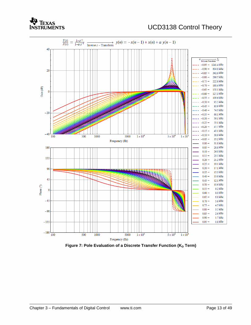
Figure 7: Pole Evaluation of a Discrete Transfer Function (KD Term)

Ti UCD3138 Control Theory
Chapter 3 – Fundamentals of Digital Control www.ti.com Page 14 of 49
Figure 8: Pole Position Time Domain Response (KD Term)

Ti UCD3138 Control Theory
Chapter 3 – Fundamentals of Digital Control www.ti.com Page 15 of 49
Figure 9 uses equation (10) to translate a series of values in the s plane to the z plane [13]. The colors used to plot values in the s plane are equivalent to the colors and values used in the z plane.
Figure 9: s Plane and z Plane Relationships

Ti UCD3138 Control Theory
Chapter 3 – Fundamentals of Digital Control www.ti.com Page 16 of 49
Several salient features are noted in table 6.
Table 6: s Plane and z Plane Salient Features
— • All stable real values in the s plane, map between 0 and 1 in the z plane. • A stable real values in the s plane that approaches -∞, approaches 0 in the z
plane.
— • Anything outside of the unit circle in the z plane is equivalent to an unstable
pole position in the s plane. • Although not explicitly shown, this is also true for complex values.
—
• The stability boundary of the imaginary y axis in the s domain is translated to the unit circle in the z domain.
• This demonstrates the warping that occurs in the z plane. • The unit circle also shows the effects of aliasing. • As the s domain values exceed ±½ the sample rate, the z plane values
continue to map to the unit circle.
—
• A diagonal line of stable values in the s plane maps to a decaying spiral centered on 0 in the z plane.
• These lines also correspond to a constant damping factor. 𝜁 = 12⋅𝑄
• This data set further demonstrates the drastic warping that occurs between s
plane values and z plane values.
— • These lines are a constant resonant frequency, ωr. • These lines are a square root function in the s domain, as shown by the
squared nature of the plot around the real axis.
— • The s plane horizontal line occurs at ±¼ the sample rate. • The z plane values occur at ±45º.
—
• The s plane values each have an imaginary value of ±½ the sample rate. • Stable complex values at ±½ the sample rate in the s plane map between -1
and 0 in the z plane. • If the s plane values have a complex element at ±½ the sample rate then
and only then do the z plane values take on a real value between -1 and 0. • In this sense the largest possible stable complex value in the s plane maps
to a negative real value in the z plane. • This mapping is consistent with the peaking that occurs at ½ the sample rate
in figure 5.
3.4 Effect of PID on Frequency Response Solving equations (31) – (34) for K0, ωz1, ωz2, and ωp2 results in equations (47) – (50).
𝐾0 =2 ⋅ 𝐾𝐼𝑇𝑠
(47)
𝜔𝑧1 =𝐾𝑃(1 − 𝛼) + 𝐾𝐼(1 + 𝛼) − 𝐾𝑃(1 − 𝛼) + 𝐾𝐼(1 + 𝛼)2 − 8(1 − 𝛼)𝐾𝐼 ⋅ 𝐾𝐷
𝑇𝑠 ⋅ (𝐾𝑃(1 + 𝛼) + 2 ⋅ 𝐾𝐷) (48)

Ti UCD3138 Control Theory
Chapter 3 – Fundamentals of Digital Control www.ti.com Page 17 of 49
𝜔𝑧2 =𝐾𝑃(1 − 𝛼) + 𝐾𝐼(1 + 𝛼) + 𝐾𝑃(1 − 𝛼) + 𝐾𝐼(1 + 𝛼)2 − 8(1 − 𝛼)𝐾𝐼 ⋅ 𝐾𝐷
𝑇𝑠 ⋅ (𝐾𝑃(1 + 𝛼) + 2 ⋅ 𝐾𝐷) (49)
𝜔𝑝1 =2𝑇𝑠
1 − 𝛼1 + 𝛼
(50)
If α = 0 equations (51) – (54) result.
𝐾0 =2 ⋅ 𝐾𝐼𝑇𝑠
(51)
𝜔𝑧1 =𝐾𝑃 + 𝐾𝐼 − (𝐾𝑃 + 𝐾𝐼)2 − 8 ⋅ 𝐾𝐼 ⋅ 𝐾𝐷
𝑇𝑠 ⋅ (𝐾𝑃 + 2 ⋅ 𝐾𝐷) (52)
𝜔𝑧2 =𝐾𝑃 + 𝐾𝐼 + (𝐾𝑃 + 𝐾𝐼)2 − 8 ⋅ 𝐾𝐼 ⋅ 𝐾𝐷
𝑇𝑠 ⋅ (𝐾𝑃 + 2 ⋅ 𝐾𝐷) (53)
𝜔𝑝1𝐴𝑝𝑝𝑟𝑜𝑎𝑐ℎ𝑒𝑠⎯⎯⎯⎯⎯⎯⎯ ∞ (54)
To understand how each PID parameter affects the frequency response, KP, KI, KD, α and fs are varied independently and the impact to the Bode plot is discussed.
Figure 10 shows effect of changing KP. When KP increases, it pushes gain’s valley up and pushes two zeros apart.
Figure 10: Effect of KP on Frequency Response.
Increasing KI shifts the low frequency gain upward and pushes first zero to the right. The second zero stays unchanged until the first zero moves to the right of the second zero.
102
103
104
105
0
5
10
15
20
25
30KP impacts on Bode Plot
Mag
nitu
de (d
B)
102
103
104
105
-90
-45
0
45
Phas
e ( °
)
Frequency (Hz)
KI=0.0216KD=4.7489Alpha=-1Fs = 400KHz
KP = 14.254
KP = 1.4254

Ti UCD3138 Control Theory
Chapter 3 – Fundamentals of Digital Control www.ti.com Page 18 of 49
Figure 11: Effect of KI on Frequency Response.
Increasing KD causes the second zero to left shift while the first zero and second pole are unchanged.
Figure 12: Effect of KD on Frequency Response.
α has a range from -1 to 1. When α = 0, the second pole is located at ∞ frequency. When α = 1, the compensator’s second pole cancels out the second zero and the compensator turns into a 1 pole 1 zero PI type controller. α directly affects the second pole position. Increasing α causes both the second pole and zero to move to the left. See section for a 3.3 discussion on negative values of α.
102
103
104
105
0
10
20
30
40
50KI impacts on Bode Plot
Mag
nitu
de (d
B)
102
103
104
105
-90
-45
0
45
Phas
e ( °
)
Frequency (Hz)
KP=1.4254KD=4.7489Alpha = -1Fs=400KHzKI = 0.216
20dB
KI = 0.0216
Z1 Z1Z2
102
103
104
105
0
5
10
15
20
25
30
35KD impacts on Bode Plot
Mag
nitu
de (d
B)
102
103
104
105
-90
-45
0
45
90
Phas
e ( °
)
Frequency (Hz)
KP = 1.4252KI = 0.0216Alpha = -1Fs = 400KHz
KD = 47.489
Z1Z2
Z2
KD = 4.7489
KD increase

Ti UCD3138 Control Theory
Chapter 3 – Fundamentals of Digital Control www.ti.com Page 19 of 49
Figure 13: Effect of α on Frequency Response.
Sampling frequency, fs, has a major impact on frequency response. It affects the low frequency gain and all pole and zero positions. Increasing fs causes the whole Bode plot to shift to higher frequencies.
Figure 14: Effect of fs on frequency response.
Table 7: Summary of PID Parameter Impacts
Control Parameters Impact on Bode Plot
KP Increasing KP • Pushes up the minimum gain between the two zeros. • Moves the two zeros apart.
KI
Increasing KI • Pushes up integration curve at low frequencies. • Gives a higher low frequency gain. • Moves the first zero to the right.
102
103
104
105
0
5
10
15
20
25
30Alpha impacts on Bode Plot
Mag
nitu
de (d
B)
102
103
104
105
-90
-45
0
45
Phas
e ( °
)
Frequency (Hz)
Kp = 1.4254KI = 0.0216KD = 4.7489Fs = 400KHz
Alpha = 1 ( 1 Pole 1 Zero)
Alpha = -1 ( 1 Pole 2 Zero)
Alpha Increase -0.5Alpha=0.5
0 -1
102
103
104
105
0
10
20
30
40
50Fs impacts on Bode Plot
Mag
nitu
de (d
B)
102
103
104
105
-90
-45
0
45
Phas
e ( °
)
Frequency (Hz)
KP = 1.4254KI = 0.0216KD = 4.7489Alpha = -1
Fs = 400KHz
20dBFs = 4MHz
Fs increase
Fs increase

Ti UCD3138 Control Theory
Chapter 3 – Fundamentals of Digital Control www.ti.com Page 20 of 49
KD Increasing KD • Shifts the second zero left. • Doesn’t impact the second pole.
α Increasing α • Shifts the second pole to the right. • Shifts the second zero to the right.
Ts = 1 / fs Increase fs • Causes the whole Bode plot to shift left.
Gai
n
Frequency
KI
KP KD α
Zero 1 Zero 2
Pole 2
Increasing fs causes the whole Bode plot to shift right.
Pole 1
Figure 15: PID Parameter Impact on Frequency Response.

Ti UCD3138 Control Theory
Chapter 4 – Compensation Examples www.ti.com Page 21 of 49
4 Compensation Examples In any closed loop system, the application of feedback requires an analysis of the stability of the system. For linear systems, this is easily done by determining the open loop gain and plotting its magnitude and phase as a Bode plot [13]. From the Bode plot, the system performance metrics of bandwidth (0 dB crossover), gain margin and phase margin can be determined. To determine the loop gain, each contributor to the open loop gain needs to be understood.
4.1 Example 1: 1ST Order System Figure 16 shows a boost converter. This discussion centers on the current loop.
LB
RLOAD
RL
Vin
Vout
RDS_ON Vsense
RD1
RD2CP1Gate
driver
IrefAnalog-to-PWM
Gain = 1
PID CompensatorKP, KI, KD, α
and Ts
RS
R3R4
CP2
Figure 16: Current Mode Control Boost Converter
Table 8: Boost Converter Component Values component Value description Vin 200V DC Input voltage. Vout 400V Nominal output voltage. Needed to determine the nominal duty cycle RL 1.48 Ω at
100KHz Equivalent resistance of the boost inductor at switching frequency.
LB 330 µH Boost inductance RDS ON 0 MOSFET turn-on resistance RS 20 mΩ Boost current sensing resistor R3 2 kΩ Input resistor of the current amplifier R4 49.9 kΩ Resistor for amplifier gain setting CP2 100pF Current amplifier low-pass capacitor PID NA Digital compensator. Its output represents PWM duty cycle. Iref NA Current reference Other parts NA Other parts are not loop related
4.1.1 Power Stage and Current Sensing Transfer Functions Figure 17 shows a simplified representation of the boost converter power stage shown in figure 16.
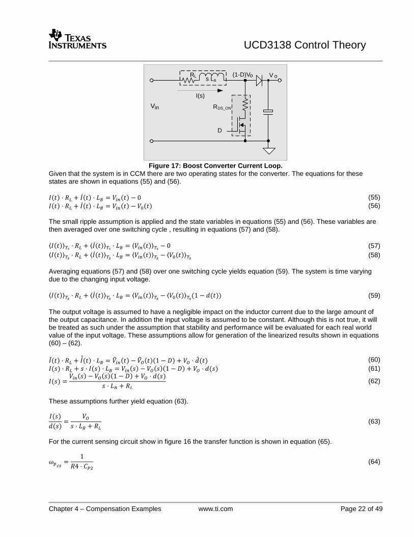
Ti UCD3138 Control Theory
Chapter 4 – Compensation Examples www.ti.com Page 22 of 49
s LBRL
Vin
(1-D)Vo
RDS_ON
D
V o
I(s)
Figure 17: Boost Converter Current Loop.
Given that the system is in CCM there are two operating states for the converter. The equations for these states are shown in equations (55) and (56). 𝐼(𝑡) ⋅ 𝑅𝐿 + 𝐼(𝑡) ⋅ 𝐿𝐵 = 𝑉𝑖𝑛(𝑡) − 0 (55) 𝐼(𝑡) ⋅ 𝑅𝐿 + 𝐼(𝑡) ⋅ 𝐿𝐵 = 𝑉𝑖𝑛(𝑡) − 𝑉0(𝑡) (56) The small ripple assumption is applied and the state variables in equations (55) and (56). These variables are then averaged over one switching cycle , resulting in equations (57) and (58). ⟨𝐼(𝑡)⟩𝑇𝑠 ⋅ 𝑅𝐿 + ⟨𝐼(𝑡)⟩𝑇𝑠 ⋅ 𝐿𝐵 = ⟨𝑉𝑖𝑛(𝑡)⟩𝑇𝑠 − 0 (57) ⟨𝐼(𝑡)⟩𝑇𝑠 ⋅ 𝑅𝐿 + ⟨𝐼(𝑡)⟩𝑇𝑠 ⋅ 𝐿𝐵 = ⟨𝑉𝑖𝑛(𝑡)⟩𝑇𝑠 − ⟨𝑉0(𝑡)⟩𝑇𝑠 (58) Averaging equations (57) and (58) over one switching cycle yields equation (59). The system is time varying due to the changing input voltage. ⟨𝐼(𝑡)⟩𝑇𝑠 ⋅ 𝑅𝐿 + ⟨𝐼(𝑡)⟩𝑇𝑠 ⋅ 𝐿𝐵 = ⟨𝑉𝑖𝑛(𝑡)⟩𝑇𝑠 − ⟨𝑉0(𝑡)⟩𝑇𝑠(1 − 𝑑(𝑡)) (59) The output voltage is assumed to have a negligible impact on the inductor current due to the large amount of the output capacitance. In addition the input voltage is assumed to be constant. Although this is not true, it will be treated as such under the assumption that stability and performance will be evaluated for each real world value of the input voltage. These assumptions allow for generation of the linearized results shown in equations (60) – (62). 𝐼(𝑡) ⋅ 𝑅𝐿 + 𝐼(𝑡) ⋅ 𝐿𝐵 = 𝑉𝑖𝑛(𝑡) − 𝑉𝑂(𝑡)(1 − 𝐷) + 𝑉𝑂 ⋅ (𝑡) (60) 𝐼(𝑠) ⋅ 𝑅𝐿 + 𝑠 ⋅ 𝐼(𝑠) ⋅ 𝐿𝐵 = 𝑉𝑖𝑛(𝑠) − 𝑉𝑂(𝑠)(1 − 𝐷) + 𝑉𝑂 ⋅ 𝑑(𝑠) (61)
𝐼(𝑠) =𝑉𝑖𝑛(𝑠) − 𝑉𝑂(𝑠)(1 − 𝐷) + 𝑉𝑂 ⋅ 𝑑(𝑠)
𝑠 ⋅ 𝐿𝐵 + 𝑅𝐿 (62)
These assumptions further yield equation (63). 𝐼(𝑠)𝑑(𝑠)
=𝑉𝑂
𝑠 ⋅ 𝐿𝐵 + 𝑅𝐿 (63)
For the current sensing circuit show in figure 16 the transfer function is shown in equation (65).
𝜔𝑝𝑐𝑠 =1
𝑅4 ⋅ 𝐶𝑃2 (64)

Ti UCD3138 Control Theory
Chapter 4 – Compensation Examples www.ti.com Page 23 of 49
𝐻𝑐𝑠(𝑠) = 𝑅𝑠𝑅4𝑅3
1𝑠
𝜔𝑝𝑐𝑠+ 1
(65)
Current sensing circuit with a low pass filter adds a pole to the loop. The pole position should be placed at between open loop crossover fc and approximately 10·fc. In the following examples, the pole is located at approximately 5·fc, which gives a good gain roll off and does not significantly degrade the phase.
From loop configuration shown in figure 18, the following open loop transfer function and closed loop transfer functions result.
𝐺𝑂𝐿(𝑠) = 𝐺𝑝𝑙𝑎𝑛𝑡(𝑠) ⋅ 𝐻𝑐𝑠(𝑠) ⋅ 𝑃𝐼𝐷(𝑠) (66)
𝐻𝑐𝑠(𝑠) =𝐺𝑝𝑙𝑎𝑛𝑡(𝑠) ⋅ 𝑃𝐼𝐷(𝑠)
1 + 𝐺𝑝𝑙𝑎𝑛𝑡(𝑠) ⋅ 𝐻𝑐𝑠(𝑠) ⋅ 𝑃𝐼𝐷(𝑠) (67)
r(s) e(s) u(s) iL(s)Gplant(s)
Hcs(s)
PID
f(s)
+
-
Figure 18: Control Loop Block Diagram
The open loop transfer function is used to generate the Bode plot, phase margin and gain margin. The closed loop transfer function can be used to perform a step response analysis.
4.1.2 Loop Compensation 1: Direct PID Tuning Current mode control power stages, such as the current loops of PFC and buck converters, are often approximated by a first order system. Since the maximum phase lag of a 1ST order system is 90º no additional zero is needed for stability. A conventional PID tuning method can be used to quickly optimize the loop compensation. The procedure is in the following paragraphs.
4.1.2.1 KP Tuning (a.k.a. zone 1 tuning) Set KI = 0 (or a very small value), KD = 0 and α = 0 (ωp2 = ∞) increase KP as much as possible until a close-loop step response starts to cause the controlled parameter to overshoot (e.g. input current). Pushing KI higher will increase bandwidth but at the cost of phase margin. Overshoot becomes more severe as phase margin decreases. The allowable overshoot is generally a system requirement. Some system can tolerate a 5% overshoot, while some others don’t allow any.
Ti UCD3138 Control Theory
Chapter 4 – Compensation Examples www.ti.com Page 24 of 49
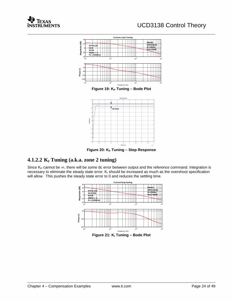
Figure 19: KP Tuning – Bode Plot
Figure 20: KP Tuning – Step Response
4.1.2.2 KI Tuning (a.k.a. zone 2 tuning) Since KP cannot be ∞, there will be some dc error between output and the reference command. Integration is necessary to eliminate the steady state error. KI should be increased as much as the overshoot specification will allow. This pushes the steady state error to 0 and reduces the settling time.
Figure 21: KI Tuning – Bode Plot
102
103
104
105
-40
-20
0
20
40Current Loop Tuning
Mag
nitu
de (d
B)
102
103
104
105
-180
-135
-90
-45
0
Phas
e ( °)
Frequency (Hz)
KP=0.125KI=0KD=0Alpha = -1Fs = 200KHz
PM=80GM=infinitefc=13KHzKdc=25dB
0 0.5 1 1.5 2 2.5 3 3.5 4 4.5 5
x 10-4
0.2
0.4
0.6
0.8
1
1.2
1.4
1.6
1.8
2
2.2Step Response
Time (sec)
Am
plit
ude
DC Error
102
103
104
105
-40
-20
0
20
40
60Current loop tuning
Mag
nitu
de (d
B)
102
103
104
105
-180
-135
-90
Phas
e ( °)
Frequency (Hz)
PM=67GM=infinitefc=13KHzKdc=48dB
KP=0.125KI=0.002KD=0Alpha = -1Fs = 200KHz

Ti UCD3138 Control Theory
Chapter 4 – Compensation Examples www.ti.com Page 25 of 49
Figure 22: KI Tuning – Step Response
PI control, can generally get a satisfactory loop response. However, if further damping is needed, KD can be used. Increasing KD will shift second zero to the left. It will boost phase margin and will damp the step response. If the phase boost causes the gain margin to become insufficient, then α can be used to provide the necessary roll off after the gain passes crossover point.
Figure 23: KD Tuning – Bode Plot
Figure 24: KD Tuning – Step Response
4.1.3 Loop Compensation 2: Pole and Zero Placement For this example, the design goal will remain the same, fc = around 10 kHz and phase margin > 60º.
0 0.5 1 1.5 2 2.5 3 3.5 4 4.5 5
x 10-4
0.2
0.4
0.6
0.8
1
1.2
1.4
1.6
1.8
2
2.2Step Response
Time (sec)
Ampl
itude
102
103
104
105
-40
-20
0
20
40
60Current Loop Tuning
Mag
nitu
de (d
B)
102
103
104
105
-135
-90
Phas
e ( °)
Frequency (Hz)
KP=0.125KI=0.002KD=0.2Alpha = -1Fs = 200KHz
PM=83GM=infinitefc=13KHzKdc=48dB
0 0.5 1 1.5 2 2.5 3 3.5 4 4.5 5
x 10-4
0.8
1
1.2
1.4
1.6
1.8
2
2.2Step Response
Time (sec)
Ampl
itude
Ti UCD3138 Control Theory
Chapter 4 – Compensation Examples www.ti.com Page 26 of 49
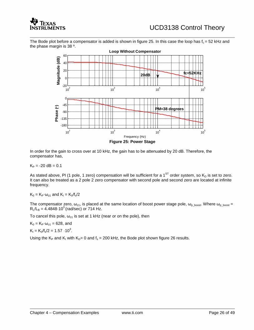
The Bode plot before a compensator is added is shown in figure 25. In this case the loop has fc = 52 kHz and the phase margin is 38 º.
Figure 25: Power Stage
In order for the gain to cross over at 10 kHz, the gain has to be attenuated by 20 dB. Therefore, the compensator has, KP = -20 dB = 0.1 As stated above, PI (1 pole, 1 zero) compensation will be sufficient for a 1ST order system, so KD is set to zero. It can also be treated as a 2 pole 2 zero compensator with second pole and second zero are located at infinite frequency. K0 = KP·ωz1 and KI = K0/fs/2 The compensator zero, ωz1, is placed at the same location of boost power stage pole, ωp_boost. Where ωp_boost = RL/LB = 4.4848·103 (rad/sec) or 714 Hz.
To cancel this pole, ωz1 is set at 1 kHz (near or on the pole), then
K0 = KP·ωz1 = 628, and
KI = K0/fs/2 = 1.57 ·103.
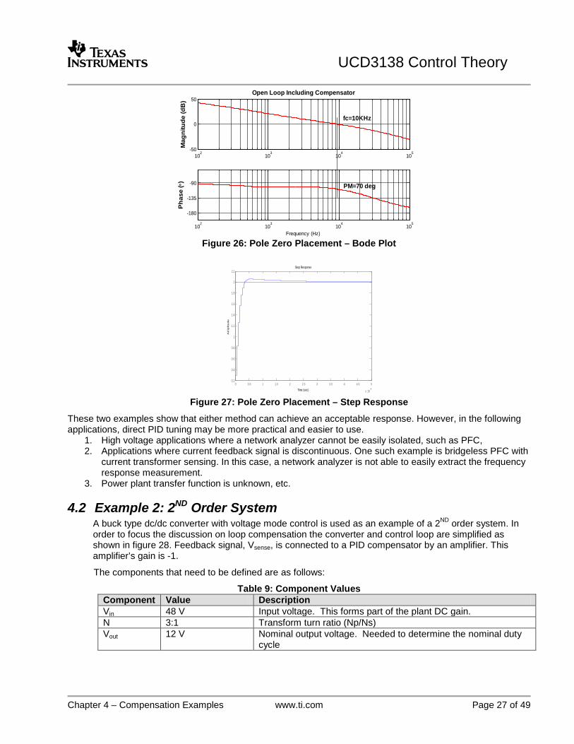
Using the KP and KI with KD= 0 and fs = 200 kHz, the Bode plot shown figure 26 results.
102
103
104
105
-20
0
20
40
60Loop Without Compensator
Mag
nitu
de (d
B)
102
103
104
105
-180
-135
-90
-45
0
Phas
e ( °)
Frequency (Hz)
20dB fc=52KHz
PM=38 degrees
Ti UCD3138 Control Theory
Chapter 4 – Compensation Examples www.ti.com Page 27 of 49
Figure 26: Pole Zero Placement – Bode Plot
Figure 27: Pole Zero Placement – Step Response
These two examples show that either method can achieve an acceptable response. However, in the following applications, direct PID tuning may be more practical and easier to use.
1. High voltage applications where a network analyzer cannot be easily isolated, such as PFC, 2. Applications where current feedback signal is discontinuous. One such example is bridgeless PFC with
current transformer sensing. In this case, a network analyzer is not able to easily extract the frequency response measurement.
3. Power plant transfer function is unknown, etc.
4.2 Example 2: 2ND Order System A buck type dc/dc converter with voltage mode control is used as an example of a 2ND order system. In order to focus the discussion on loop compensation the converter and control loop are simplified as shown in figure 28. Feedback signal, Vsense, is connected to a PID compensator by an amplifier. This amplifier’s gain is -1.
The components that need to be defined are as follows:
Table 9: Component Values Component Value Description Vin 48 V Input voltage. This forms part of the plant DC gain. N 3:1 Transform turn ratio (Np/Ns) Vout 12 V Nominal output voltage. Needed to determine the nominal duty
cycle
102
103
104
105
-50
0
50Open Loop Including Compensator
Mag
nitu
de (d
B)
102
103
104
105
-180
-135
-90P
hase
( °)
Frequency (Hz)
fc=10KHz
PM=70 deg
0 0.5 1 1.5 2 2.5 3 3.5 4 4.5 5
x 10-4
0.2
0.4
0.6
0.8
1
1.2
1.4
1.6
1.8
2
2.2Step Response
Time (sec)
Am
plit
ude

Ti UCD3138 Control Theory
Chapter 4 – Compensation Examples www.ti.com Page 28 of 49
RD 8 mΩ This is the total resistance during D period, including reflected primary side FET’s resistance, transformer resistance and secondary synchronous MOSFET resistance.
R1-D 8 mΩ The total combined resistance of synchronous MOSFETs and maybe power transformer secondary winding DC resistance during 1-D period, depended on the given topology.
RL 2 mΩ DC resistance of the inductor L 2 µH Inductor inductance C1 1329 µF Combined (summed) capacitance of all ceramic caps on the
output RC1 1 mΩ Parallel combination of ESR for ceramic caps. LC1 0 µH Effective series inductance (ESL) of ceramic caps RD1 11 kΩ Voltage sensing divider top resistor RD2 1 kΩ Voltage sensing divider bottom resistor Cz 0 µF Voltage sensing zero capacitor Cp 1 nF Voltage sensing low-pass filter cap ( pole capacitor) RLOAD 1 Ω Load resistance fs 200 kHz Sampling frequency
Note: Parameter values are based on 48 V Hard Switching Full Bridge EVM design.
LO
C1
RC11RLOAD
RL
Vin
Vout
R1-D
RD
Vsense
RD1
RD2CP
Gate driver
CZ
LC1
/N
VrefAnalog-to-PWM
Gain = 1
PID CompensatorKP,KI,KD, α
and Ts
Gain = -1
Figure 28: Equivalent Buck Converter
4.2.1 Power Stage and Voltage Sensing Circuit Transfer Function The effective series resistance, Rs is the total averaged series resistance and consists of the dc resistance of the inductor, RL, and the equivalent MOSFET resistances RD. For the small signal ac transfer function, the average resistance presented by the two MOSFET can be calculated as:
𝐷 =𝑉𝑂𝑉𝐼𝑁
(68)
𝑅𝑛𝑜𝑑𝑒 = 𝑅𝐷 ⋅ 𝐷 + 𝑅1−𝐷 ⋅ (1 − 𝐷) (69) 𝑅𝑆 = 𝑅𝑛𝑜𝑑𝑒 + 𝑅𝐿 (70)
There may be several capacitors on the output. Typically there will be large valued capacitors to provide the bulk energy storage and smaller valued ceramic capacitors with lower effective series resistance (esr) and

Ti UCD3138 Control Theory
Chapter 4 – Compensation Examples www.ti.com Page 29 of 49
effective series inductance (esl) values to supply high frequency current. Each capacitor type can be considered by equation (71).
𝑍𝐶𝑛(𝑠) = 1
𝑠 ⋅ 𝐶𝑛+ 𝑠 ⋅ 𝑒𝑠𝑙𝑛 + 𝑒𝑠𝑟𝑛
1𝑁𝑐𝑛
(71)
The combined effect of all the different capacitors can be calculated using equation (72).
𝑍𝐶𝑇𝑜𝑡𝑎𝑙(𝑠) = 𝑍𝐶𝑛(𝑠)−1𝑁
𝑛=1
−1
(72)
Using these relationships along with figure 28 the plant transfer function Gplant(s) can be determined.
From the loop configuration shown in figure 29 the open loop and closed loop transfer functions can be derived as shown in equations (73) and (74).
𝐺𝑂𝐿(𝑠) = 𝐺𝑝𝑙𝑎𝑛𝑡(𝑠) ⋅ 𝐺𝐷𝐼𝑉(𝑠) ⋅ 𝑃𝐼𝐷(𝑠) (73)
𝐻𝑐𝑠(𝑠) =𝐺𝑝𝑙𝑎𝑛𝑡(𝑠) ⋅ 𝑃𝐼𝐷(𝑠)
1 + 𝐺𝑝𝑙𝑎𝑛𝑡(𝑠) ⋅ 𝐺𝐷𝐼𝑉(𝑠) ⋅ 𝑃𝐼𝐷(𝑠) (74)
r(s) e(s) u(s) vo(s)Gplant(s)
Gdiv(s)
PID
f(s)
+
-
Figure 29: Loop Configuration.
4.2.2 Loop Compensation Procedure by Using 2-Pole 2-Zero Analog Compensator
4.2.2.1 Loop Compensation goals: • Crossover frequency fc is about 20 kHz • Phase margin > 60º.
4.2.2.2 2ND System Tuning Procedure 1. Determine the second order system’s resonant frequency.
𝑓𝑟 = 1
2⋅𝜋√𝐿𝑜⋅𝐶1 = 3.08 kHz (75)
2. Plot Power stage and feedback network frequency response.

Ti UCD3138 Control Theory
Chapter 4 – Compensation Examples www.ti.com Page 30 of 49
Figure 30: Plant Frequency Response
To get 20 kHz crossover frequency, a compensator should have 30 dB of gain at the desired cross over frequency and a phase boost of 180º.
3. To boost the phase by 180º, a 2 pole 2 zero compensator is needed and should be located at 1/10 of fc.
fz1 = fz2 = 2 kHz
4. Place the second pole of the compensation at a frequency 10 times higher than fc to start with. This way it will not affect the expected gain and phase at fc.
5. Plot compensator’s frequency response and vary K0 to get desired gain. Vary K0 so the gain at fc is 30 dB,
Figure 31: Analog Compensator Plot
6. Plot Open-Loop frequency response,
102
103
104
105
-60
-40
-20
0
20Open Loop Without Compensator
Mag
nitu
de (d
B)
102
103
104
105
-180
-135
-90
-45
0
Phas
e ( °)
Frequency (Hz)
-30dB
102
103
104
105
10
20
30
40
50Compensator
Mag
nitu
de (d
B)
102
103
104
105
-90
-45
0
45
90
Phas
e ( °)
Frequency (Hz)
30dB
80deg

Ti UCD3138 Control Theory
Chapter 4 – Compensation Examples www.ti.com Page 31 of 49
Figure 32: Analog Placement – Bode Plot
Figure 33: Analog Placement – Step Response
After adding the tuned compensator to the loop, the open loop Bode plot can be generated. It can be seen that both phase margin and crossover frequency design goals were met.
7. Convert control parameters to component values
The compensation above uses real poles and zeros. The control parameters can be converted to circuit component values by using the equations in section 3.2.
Table 10: Resistor and Capacitor Values
R1 1 kΩ
R2 36.2 kΩ
C1 2.2 nF
C2 2.2 nF
C3 22 pF
Compensation parameters designed in s domain can be converted to discrete z domain.
Following parameters are obtained from the analog compensation.
Table 11: Raw Gains
K0 0.45e5
102
103
104
105
-20
0
20
40Buck Converter Open loop Bode Plot
Mag
nitu
de (d
B)
102
103
104
105
-135
-90
-45
0Ph
ase
( °)
Frequency (Hz)
fc = 22KHzPM=80 deg
Kdc=45000fp2 = 200KHzfz1=fz2 = 2KHz
0 1 2 3 4 5 6 7
x 10-4
4
5
6
7
8
9
10
11
12
13Step Response
Time (sec)
Ampl
itude

Ti UCD3138 Control Theory
Chapter 4 – Compensation Examples www.ti.com Page 32 of 49
ωz1 12560
ωz2 12560
ωp1 6.28*200e3
They can be converted PID parameters. Table 12: PID Values
KP 7.129777
KI 0.1125
KD 0.8481896
α -0.5169082
4.2.3 Loop Compensation Procedure by Using PID Procedure of second-order system tuning,
1. Determine the second order system’s resonant frequency
𝑓𝑟 = 1
2⋅𝜋√𝐿𝑜⋅𝐶1 = 3.08 kHz (76)
2. If the resonant frequency is beyond of power supply frequency bandwidth, the power plant of the converter basically turns into a 1ST order system. Direct PID tuning can be used to optimize loop compensation.
3. For most cases, power supply bandwidth needs to push higher than power plant resonant frequency. The two system poles cause 180º of phase delay, and a two pole two zero compensator becomes necessary.
4. Preselect the low frequency gain K0 value to be 10k (most analog amplifier DC gain range is from 10k to 100k). Choose the sampling frequency to be the same as switching frequency, then:
𝐾𝐼 = 𝐾0
2⋅𝑓𝑠 = 0.025 (77)
5. Place second pole at infinite frequency (ωp2 = ∞) by setting α = 0
6. Place the two compensator zeros at 1/10 of expected crossover frequency (20Khz) and calculate KP and KD as follows,
KP= K0 (ωz2+ωz1)/( ωz1* ωz2) = 1.59
KD= 2·K0·fs/( ωz1* ωz2) = 101.4
If it is not clear where the zeros should be put, a loop frequency response without the compensator should be generated.
The system with the calculated PID values has the following Bode plot and step response,

Ti UCD3138 Control Theory
Chapter 4 – Compensation Examples www.ti.com Page 33 of 49
Figure 34: PID – Bode Plot
Figure 35: PID – Step Response
7. Now vary KI and α to fine tune the loop and get the best combination of phase margin, gain margin and crossover frequency. KI is increased to get a better dc gain. Increase α to move the second pole to the left. The pole will provide additional gain margin but it should not lower phase margin and crossover frequency much.
When using digital PID to compensate loop, the design has more degrees of freedom to place zeros. Complex zeros can be used to achieve an alternate performance. More details on this are discussed in section 5.4.
ωz1 = 2.4902e+003 -1.8640e+004i and
ωz2 = 2.4902e+003 +1.8640e+004i
Note: A pair of complex zeros means a negative value of C1
102
103
104
105
-20
-10
0
10
20
30Voltage Loop with calculated PID Parameters
Mag
nitu
de (d
B)
102
103
104
105
-90
-45
0
45Ph
ase
( °)
Frequency (Hz)
KP =1.59KI = 0.025KD = 101.4Alpha = -1Fs = 200KHz
PM=93GM=InfiniteFc=20KHz
0 0.5 1 1.5
x 10-3
4
5
6
7
8
9
10
11
12
13Step Response
Time (sec)
Am
plit
ude

Ti UCD3138 Control Theory
Chapter 4 – Compensation Examples www.ti.com Page 34 of 49
Figure 36: PID – Bode Plot (KI)
Figure 37: PID – Step Response (KI)
102
103
104
105
-20
0
20
40
60Optimized Voltage Loop
Ma
gn
itu
de
(d
B)
102
103
104
105
-135
-90
-45
Ph
as
e (°)
Frequency (Hz)
KP=1.59KI = 0.3KD=101.4Alpha = -0.5Fs = 200KHz
PM =86GM = Infinitefc = 28KHz
0 1 2 3 4 5 6 7
x 10-4
4
5
6
7
8
9
10
11
12
13Step Response
Time (sec)
Am
plitu
de

Ti UCD3138 Control Theory
Chapter 5 – UCD3138 Compensator www.ti.com Page 35 of 49
5 UCD3138 Compensator
250ps DPWM
EADC
CLA AFE
14 bit DAC97.65nV/LSB
9 bit ADC1LSB/1mV
Ramp Counter
0
PRD
EAP
EAN
Converter
Duty Cycle (d)VOUT Feedback (VFB)
Figure 38: General UCD3138 Block Diagram
5.1 Error ADC Gain The analog front end has a programmable block that allows the user to configure the resolution of the front end to according to table 13.
Table 13: Front End Resolution AFE EADC Resolution
0 8 mV 1 4 mV 2 2 mV 3 1 mV
The actual ADC shown in figure 38, has only 6 bits, however these bits are sign extended to provide a constant gain from the sensed output voltage to the input to the CLA. Again the resolution of the front end with these different AFE settings results as shown in table 13. KEADC = 1000 (78)
5.2 CLA Structure and Implementation
5.2.1 CLA Structure: PID Form and Transfer Function UCD31xx uses a PID form control law accelerator (CLA). The three branches of PID are configured in parallel form as shown in figure 39.

Ti UCD3138 Control Theory
Chapter 5 – UCD3138 Compensator www.ti.com Page 36 of 49
z-1 e(n )
KP
KI
KD
z-1
-
e(n-1)
y(n)
z-1 α
yP (n)
yI (n)
yD(n)
+ +
+
Figure 39: PID Form CLA Structure
A filter output y can be defined from figure 39 that is the sum of a proportional, integral and derivative gain.
𝑦(𝑛) = 𝑦𝑃(𝑛) + 𝑦𝐼(𝑛) + 𝑦𝐷(𝑛) (79) 𝑦𝑃(𝑛) = 𝐾𝑃 ⋅ 𝑒(𝑛) (80) 𝑦𝐼(𝑛) = 𝑦𝐼(𝑛 − 1) + 𝐾𝐼 ⋅ (𝑒(𝑛) + 𝑒(𝑛 − 1)) (81) 𝑦𝐷(𝑛) = 𝛼 ⋅ 𝑦𝐷(𝑛 − 1) + 𝐾𝐷 ⋅ (𝑒(𝑛) − 𝑒(𝑛 − 1)) (82)
The z transform of these difference equations is:
𝑦(𝑧) = 𝑦𝑃(𝑧) + 𝑦𝐼(𝑧) + 𝑦𝐷(𝑧) (83) 𝑦𝑃(𝑧) = 𝐾𝑃 ⋅ 𝑒(𝑧) (84) 𝑦𝐼(𝑧) = 𝑧−1 ⋅ 𝑦𝐼(𝑧) + 𝐾𝐼 ⋅ (𝑒(𝑧) + 𝑧−1 ⋅ 𝑒(𝑧)) (85) 𝑦𝐷(𝑧) = 𝛼 ⋅ 𝑧−1 ⋅ 𝑦𝐷(𝑧) + 𝐾𝐷 ⋅ (𝑒(𝑧) − 𝑧−1 ⋅ 𝑒(𝑧)) (86)
Then the transfer function in the z domain is:
𝑦(𝑧)𝑒(𝑧)
= 𝐾𝑃 + 𝐾𝐼1 + 𝑧−1
1 − 𝑧−1+ 𝐾𝐷
1 − 𝑧−1
1 − 𝛼 ⋅ 𝑧−1 (87)
5.2.2 CLA Hardware Implementation Figures 40 through 42 illustrate the calculation details of the PID CLA. Data formats are given to next to each node. In the notation Sn.m means that the values is signed (if no “S” is present then the data is unsigned), “n” is the number of digits available before the decimal point and “m” is the number after the decimal point. All number formats are in binary.

Ti UCD3138 Control Theory
Chapter 5 – UCD3138 Compensator www.ti.com Page 37 of 49
Figure 40: PID Filter Branch and Calculation Implementation
Figure 41: PID Summation and CLA Output

Ti UCD3138 Control Theory
Chapter 5 – UCD3138 Compensator www.ti.com Page 38 of 49
Figure 42: Translation from CLA output to Duty Cycle and Period
At the beginning of the translation stage, the PID output is multiplied by one of several 14 bit unsigned numbers, giving a 38 bit output. This number is right shifted by 19 bits and rounded to give the unsigned 18 bit value. This number is used for DPWM pulse width (250 ns resolution). The DPWM Period is 14 bits with 4 ns resolution. This number should be converted to a value with the same 250nS resolution and then used as an equivalent ramp.
Connecting all EADC, CLA, DPWM and stages together results in equation (88).
𝑑(𝑧)𝑣𝑓𝑏(𝑧)
= −1000 𝐾𝑃 + 𝐾𝐼1 + 𝑧−1
1 − 𝑧−1+ 𝐾𝐼
1 − 𝑧−1
1 − 𝛼 ⋅ 2−8 ⋅ 𝑧−1
2𝑆𝐶 ⋅ 𝐾𝐶𝑂𝑀𝑃 ⋅ 2−19
24(𝑃𝑅𝐷 + 1) 𝑒−𝑠⋅𝑇𝑑𝑒𝑙𝑎𝑦 (88)
𝑇𝑑𝑒𝑙𝑎𝑦 = 𝑡𝑑 + 𝐷 ⋅24 ⋅ (𝑃𝑅𝐷 + 1) ⋅ 𝑇𝐷𝑃𝑊𝑀
2 (89)
Equation (89) assumes that the sample trigger point has been placed 𝑡𝑑 prior to the end of the period. In addition, it also assumes that the DPWM update window has been set to end of period. Under these conditions 𝑡𝑑, represents the computational delay of the controller. 𝐷 ⋅ 2
4⋅(𝑃𝑅𝐷+1)⋅𝑇𝐷𝑃𝑊𝑀2
represents the time that elapses before this information impacts the output duty cycle [27]. In normal mode it is possible to get a DPWM update

Ti UCD3138 Control Theory
Chapter 5 – UCD3138 Compensator www.ti.com Page 39 of 49
event at every DPWM edge. This applies to both half cycles of the full bridge and half bridge topologies. If the system does not or cannot support normal mode then this second delay term could be longer by as much as 24⋅(𝑃𝑅𝐷+1)⋅𝑇𝐷𝑃𝑊𝑀
2.
Since α has a valid range is from -1 to 1, it needs to be normalized for transfer function calculation. The normalization is implemented by multiplying the 9 bit signed α and then dropping off 8 bits of the result. In transfer function, α is divided by 28 (not including sign bit) for normalization.
5.3 GUI Model Equations This section provide the GUI model equations (table 14) as well as the transformation equations used to convert between the different models shown in table 14.
Table 14: GUI Transfer Functions
Table 15: Device Registers to Complex Zeros

Ti UCD3138 Control Theory
Chapter 5 – UCD3138 Compensator www.ti.com Page 40 of 49
Table 16: Real Zeros to Complex Registers
Table 17: Device Registers to Real Zeros
Table 18: Real Zeros to Device Registers
In addition to the GUI equations tables 19 and 20 show the formulas for converting between equations (30) and (88).

Ti UCD3138 Control Theory
Chapter 5 – UCD3138 Compensator www.ti.com Page 41 of 49
Table 19: Normalized PID to Register PID
Table 20: Register PID to Normalized PID
Table 21: Allowable Register Integer Values -32768 ≤ KP ≤ 32767 -32768 ≤ KI ≤ 32767 -32768 ≤ KD ≤ 32767
-256 ≤ α ≤ 255 0 ≤ PRD ≤ 16384
0 ≤ KCOMP ≤ 16384 -4 ≤ SC ≤ 3
NOS ∈ 1, 2, 4, 8
Figure 43 shows a model comparison between the target analog compensator performance and the resulting actual performance of the UCD3138 device. In addition to the constraints shown on the plot the following conditions shown in table 22 were applied.
Table 22: Bode Plot Conditions KCOMP = PRD
SC = 0 Over Sampling Rate, NOS = 1 Computation Delay, td = 500 ns Duty Cycle Delay, D/fs/2 = 1 μs

Ti UCD3138 Control Theory
Chapter 5 – UCD3138 Compensator www.ti.com Page 42 of 49
Using figure 3 and equations (21) – (29) are used to generate the analog compensator parameters and performance shown in figure 43.
Figure 43: UCD3138 Model Comparison

Ti UCD3138 Control Theory
Chapter 5 – UCD3138 Compensator www.ti.com Page 43 of 49
Figure 44: Measured Results
Figure 44 shows excellent correlation between the measured results and the model (88). At low frequencies a sizable deviation between the model and measurement is observed. This error is due to the finite limitations of the analyzer to resolve a small signal [22][23]. If a 50 mV disturbance were injected into the loop that would require that the input signal be approximately 0.15 mV on the input. It’s not difficult to imagine that the analyzer would have difficulties resolving the magnitude and phase of a signal this small.
5.4 Complex Zeros

Ti UCD3138 Control Theory
Chapter 5 – UCD3138 Compensator www.ti.com Page 44 of 49
The compensation structure of the UCD3138 provides the flexibility to do many things that are not possible with a conventional controller. One such thing is the placement of complex zeros. While advantageous in many applications, care should be used with their application. It would be wrong to assume that nulling out the peaking in a typical second order plant will yield the best load transient response. For example take the plant shown in figure 45.
Figure 45: Compensation Comparisons

Ti UCD3138 Control Theory
Chapter 5 – UCD3138 Compensator www.ti.com Page 45 of 49
As shown in figure 45 it is possible to compensate the loop with either complex zeros or real zeros. The complex zeros are capable of completely nulling out the high Q effect of the plant. The results of this compensation are shown in figure 46. Both of these systems have approximately the same bandwidth.
Figure 46: Compensation Comparison – Loop Response
This is a great example of where bandwidth does not adequately describe the targeted closed loop behavior. If bandwidth were the only requirement these two systems would be equivalent. As will be shown shortly the case with the real zeros has far superior performance. Figure 47 shows the output impedance of each of the open loop system and the closed loop systems with each of the resulting loop gains shown in figure 46. As expected the open loop plant has a large output impedance at

Ti UCD3138 Control Theory
Chapter 5 – UCD3138 Compensator www.ti.com Page 46 of 49
the resonant frequency, owing to the high Q nature of the output filter. This naturally suggests that the addition of loop gain at these critical frequencies can help to reduce this peak. This is in fact what is achieved with the real zeros. By allowing the gain to peak in the loop gain, the compensation offers the system additional “muscle” to reduce the peaking of the output impedance. Reducing the output impedance is directly equivalent to improving the load transient response as is shown in figure 48.
Figure 47: ZOUT Impedance Plots
Figure 48 shows the resulting output voltage disturbance when a step load transient is applied to the output. As the ZOUT plots in figure 47 suggest the resulting output voltage deviation and subsequent settling time are greatly reduced compared to the complex zero compensation. This occurs in spite of the fact that the bandwidth of the two systems is the same.

Ti UCD3138 Control Theory
Chapter 5 – UCD3138 Compensator www.ti.com Page 47 of 49
Figure 48: Load Step Response

Ti UCD3138 Control Theory
Chapter 6 – References www.ti.com Page 48 of 49
6 References
6.1 Available UCD3138 Related Literature • UCD3138 Datasheet, Texas Instruments, 2011 • UCD3138 program manuals • EVM documentation • Firmware source code
6.2 References [1] Adair, R., "Design Review: A 300 W, 300 kHz Current-Mode, Half-Bridge Converter with Multiple
Outputs Using Coupled Inductors,” Texas Instruments Power Supply Seminar, http://www.ti.com/lit/ml/slup083/slup083.pdf.
[2] Rossetto, L.; Spiazzi, G.; , "Design considerations on current-mode and voltage-mode control methods for half-bridge converters," Applied Power Electronics Conference and Exposition, 1997. APEC '97 Conference Proceedings 1997., Twelfth Annual , vol.2, no., pp.983-989 vol.2, 23-27 Feb 1997.
[3] Mammano, R., ”Load Sharing with Paralleled Power Supplies,” Texas Instruments Power Supply Seminar, http://www.ti.com/lit/ml/slup094/slup094.pdf.
[4] UCD31xx Fusion digital Power Peripherals Programmer’s Manual, Texas Instruments Incorporated. [5] http://www.plugloadsolutions.com/80PlusPowerSupplies.aspx. [6] Huang, Hong; SEM1900, Designing an LLC Resonant Half-Bridge Power Converter; Texas
Instruments, Manchester, NH, 2010. [7] Bing Lu; Wenduo Liu; Yan Liang; Lee, F.C.; van Wyk, J.D.; , "Optimal design methodology for LLC
resonant converter," Applied Power Electronics Conference and Exposition, 2006. APEC '06. Twenty-First Annual IEEE , vol., no., pp. 6 pp., 19-23 March 2006.
[8] Ya Liu; High Efficiency Optimization of LLC Resonant Converter for Wide Load Range, Virginia Polytechnic Institute and State University, Master’s Thesis, 2007.
[9] Yiqing Ye; Chao Yan; Jianhong Zeng; Jianping Ying; , "A novel light load solution for LLC series resonant converter," Telecommunications Energy Conference, 2007. INTELEC 2007. 29th International , vol., no., pp.61-65, Sept. 30 2007-Oct. 4 2007.
[10] Maksimovic, D.; Erickson, R.; Griesbach, C.; , "Modeling of cross-regulation in converters containing coupled inductors," Applied Power Electronics Conference and Exposition, 1998. APEC '98. Conference Proceedings 1998., Thirteenth Annual , vol.1, no., pp.350-356 vol.1, 15-19 Feb 1998.
[11] Suntio, T.; Glad, A.; Waltari, P.; , "Constant-current vs. constant-power protected rectifier as a DC UPS system's building block," Telecommunications Energy Conference, 1996. INTELEC '96., 18th International , vol., no., pp.227-233, 6-10 Oct 1996.
[12] Lazar, J.F.; Martinelli, R.; , "Steady-state analysis of the LLC series resonant converter," Applied Power Electronics Conference and Exposition, 2001. APEC 2001. Sixteenth Annual IEEE , vol.2, no., pp.728-735 vol.2, 2001.
[13] G. Franklin, J. Powell and M. Workman, Digital Control of Dynamic Systems, Prentice Hall, 3rd Edition, 1997.
[14] Texas Instruments Fusion digital power designer, http://focus.ti.com/docs/toolsw/folders/print/fusion_digital_power_designer.html.
[15] A. Costabeber, P. Mattavelli, and S. Saggini, “Digital Time-Optimal Phase Shedding in Multi-Phase Buck Converters,” IEEE Transactions on Power Electronics, Volume: PP , Issue 99, 2010.
[16] X. Zhou, M. Donati, L. Amoroso, and F. Lee, “Improved Light-Load Efficiency for Synchronous Rectifier Voltage Regulator Module,” IEEE Transactions on Power Electronics, Volume 15, Issue 5, September 2000.
[17] R. Erickson and D. Maksimovic, Fundamentals of Power Electronics, 2nd Edition, Kluwer Academic Press, 2001.
[18] M. Hagen, “In Situ Transfer Function Analysis: Measurement of system dynamics in a digital power supply,” Digital Power Forum, 2006.

Ti UCD3138 Control Theory
Chapter 6 – References www.ti.com Page 49 of 49
[19] M. Shirazi, J. Morroni, A. Dolgov, R. Zane and D. Maksimovic, "Integration of frequency response measurement capabilities in digital controllers for DC-DC converters," IEEE Transactions on Power Electronics, Volume 23, Issue 5, pp. 2524 – 2535, Sep. 2008.
[20] N. Kong, A. Davoudi, M. Hagen, E. Oettinger, M. Xu, D. Ha, and F. Lee; “Automated System Identification of Digitally-Controlled Multi-phase DC-DC Converters,” IEEE APEC 2009 , Page(s): 259 – 263.
[21] A. Oppenheim, R. Schafer and J. Buck; Discrete-Time Signal Processing, 2nd Edition, Prentice-Hall Signal Processing Series, 1999.
[22] Venable industries frequency response analyzer, http://www.venable.biz/. [23] Ridley Engineering frequency response analyzer, http://www.ridleyengineering.com/analyzer.htm. [24] R. Ridley, A New Continuous-Time Model for Current-Mode Control, IEEE Transactions on Power
Electronics, April, 1991, pp. 271-280. [25] L. Dixon, Current-mode control of switching power supplies, Texas Instruments SLUP075, 1985,
http://focus.ti.com/lit/ml/slup075/slup075.pdf. [26] T. Suntio, A. Glad, P. Waltari; “Constant-current vs. constant-power protected rectifier as a DC UPS
system's building block,” Telecommunications Energy Conference, 1996. INTELEC '96., 18th International, 1996 , Page(s): 227 - 233.
[27] R. D. Middlebrook, “Predicting Modulator Phase Lag in PWM Converter Feedback Loops,” Proc. Eighth International Solid-State Power Conversion Conference (Powercon 8), H4.1—H4.6, Apr. 1981.