ucc28782 system bring up guideline and common issues
TRANSCRIPT

Application NoteUCC28782 System Bring Up Guideline and Common Issues
ABSTRACTThis application note presents a step-by-step debug process to help designers debug their UCC28782 high-frequency active clamp flyback (ACF) converters in an efficient manner. Firstly, VDD start and typical system operation waveforms are presented, then the frequently happen protections waveforms are demonstrated, finally common issues and solutions are shown. Assume the reader has read the UCC28782 data sheet in detail and has some basic knowledge of ACF topology before reading this application note. Together, with another application note Debugging UCC28780 ACF Converter Start-up Issues, we can start the ACF journey.
Table of Contents1 Initial Board Visual Inspection and Start-up Check ............................................................................................................32 Typical System Operating Waveforms .................................................................................................................................6
2.1 SBP2 Mode........................................................................................................................................................................ 62.2 SBP1 Mode........................................................................................................................................................................ 62.3 LPM mode..........................................................................................................................................................................72.4 LPM to ABM Mode Transition............................................................................................................................................ 72.5 ABM Mode......................................................................................................................................................................... 82.6 ABM to AAM Mode Transition............................................................................................................................................92.7 AAM Mode......................................................................................................................................................................... 9
3 Typical System Protection Waveforms............................................................................................................................... 113.1 Over-Power Protection (OPP).......................................................................................................................................... 113.2 Output Overvoltage Protection (OVP)..............................................................................................................................123.3 Output Short-Circuit Protection (SCP)............................................................................................................................. 13
4 Common Issues and Solutions........................................................................................................................................... 154.1 VDD Boost Converter Survival Mode...............................................................................................................................154.2 10% Load Efficiency Might not Meet spec. in USB-PD Application, Especially at 5 V/9 V Output Condition.................. 164.3 Transient.......................................................................................................................................................................... 17
5 References............................................................................................................................................................................ 23
List of FiguresFigure 1-1. Probing UCC28782 Pins with a Digital Multimeter.................................................................................................... 3Figure 1-2. VDD Start Up and Hiccup at Below Brown In Voltage...............................................................................................4Figure 1-3. VDD Restart.............................................................................................................................................................. 4Figure 1-4. CS Pin Fault Detection - Only 1 Pulse With 2us Width............................................................................................. 5Figure 1-5. Brown-in Voltage Detection – 4 Consecutive Pulses................................................................................................ 5Figure 2-1. SBP2 Mode Operation Waveform............................................................................................................................. 6Figure 2-2. SBP1 Mode Operation Waveform............................................................................................................................. 7Figure 2-3. LPM Mode Operation Waveform...............................................................................................................................7Figure 2-4. LPM to ABM Mode Transition....................................................................................................................................8Figure 2-5. ABM Mode PWML Pulse NSW=2...............................................................................................................................8Figure 2-6. ABM Mode PWML Pulse NSW=7...............................................................................................................................9Figure 2-7. ABM to AAM Mode Transition................................................................................................................................... 9Figure 2-8. AAM Mode Medium Load........................................................................................................................................10Figure 2-9. AAM Mode Heavy Load.......................................................................................................................................... 10Figure 3-1. OPP Delay to Action................................................................................................................................................11Figure 3-2. OPP Action.............................................................................................................................................................. 11Figure 3-3. OVP Delay to Action................................................................................................................................................12Figure 3-4. OVP Delay to Action (Zoom In)............................................................................................................................... 12Figure 3-5. OVP Action..............................................................................................................................................................13
www.ti.com Table of Contents
SLUAAF9 – SEPTEMBER 2021Submit Document Feedback
UCC28782 System Bring Up Guideline and Common Issues 1
Copyright © 2021 Texas Instruments Incorporated

Figure 3-6. SCP Delay to Action................................................................................................................................................13Figure 3-7. SCP Action.............................................................................................................................................................. 14Figure 4-1. Boost Inductor DCR > 1 ohm.................................................................................................................................. 15Figure 4-2. Boost Inductor DCR = 0.56 ohm............................................................................................................................. 15Figure 4-3. Operating at SBP1 Mode........................................................................................................................................ 16Figure 4-4. Operating at SBP2 Mode........................................................................................................................................ 16Figure 4-5. IPC Pin Resistor Setting..........................................................................................................................................17Figure 4-6. SR FET Non-ZCS Turn Off......................................................................................................................................17Figure 4-7. SR FET ZCS Turn Off..............................................................................................................................................18Figure 4-8. SR Vds Overstress When Survival Mode Kick In....................................................................................................18Figure 4-9. SR Vds Overstress – Zoom In.................................................................................................................................19Figure 4-10. PWMH Partial Turn On..........................................................................................................................................20Figure 4-11. PWMH Partial Turn On – Zoom In.........................................................................................................................20Figure 4-12. Level Based Isolation Driver Architecture............................................................................................................. 21Figure 4-13. Edge Based Isolation Driver Architecture..............................................................................................................21Figure 4-14. Isolator Change to ISO7310..................................................................................................................................22
TrademarksAll trademarks are the property of their respective owners.
Trademarks www.ti.com
2 UCC28782 System Bring Up Guideline and Common Issues SLUAAF9 – SEPTEMBER 2021Submit Document Feedback
Copyright © 2021 Texas Instruments Incorporated

1 Initial Board Visual Inspection and Start-up CheckBefore powering up the design board, the first step is to thoroughly review the design to make sure all design parameters are calculated properly. The Excel Design Calculator is a helpful tools to check the accuracy of the design. It is recommended to do a visual inspection to check for the following:
• Solder bridges• Solder balls• Solder skips• Cold solder joints• Lifted pads
After visual inspection, the user can also use a multimeter to check the solder, Multimeter locked to diode location, Red probe connected to IC ground, Black probe connected to each pin. There should be a ~0.5 V-0.7 V voltage presents on the multimeter, if not, check solder of this pin. Figure 1-1 demonstrates probing UCC28782 Pins with a digital multimeter.
Figure 1-1. Probing UCC28782 Pins with a Digital Multimeter
When the solder inspection is complete, the board can input a low voltage, next steps are input short-circuit investigation / HV start circuits operation check / CS pin fault detection and input brown in voltage (startup voltage) detection:
1. Step 1: Set input voltage source to Vin=5 Vrms while limiting its current to 0.5 A, measure the input current. After a brief low inrush peak current, there should be almost zero continuous input current, if an excessive current is observed, there may be a short or abnormally low impedance in the circuit.
2. Step 2: If zero current is observed. Move to VDD pin to check if HV start circuits working properly, 25 Vrms voltage implied on the input, the captured waveform of VDD as shown in Figure 1-2: If VDD voltage can be charged to ~17.5 V, it indicates the HV start circuits working normal. if not please refer to Debugging UCC28780 ACF Converter Start-up Issues section 7.3, Start-up Failure Due to VDD Clamped Low.
www.ti.com Initial Board Visual Inspection and Start-up Check
SLUAAF9 – SEPTEMBER 2021Submit Document Feedback
UCC28782 System Bring Up Guideline and Common Issues 3
Copyright © 2021 Texas Instruments Incorporated

Figure 1-2. VDD Start Up and Hiccup at Below Brown In Voltage
3. Step 3: Zoom in waveform at the point when VDD reaches to its turn on threshold (17.5 V), capture low side driver signal PWML, if only one pulse with a width of 2us is observed, see Figure 1-4, this is the correct behavior at the input voltage which lower than start up voltage. Please refer to Debugging UCC28780 ACF Converter Start-up Issues section 6.1 Observation of Zero or Only One PWML Pulse.
Figure 1-3. VDD Restart
Initial Board Visual Inspection and Start-up Check www.ti.com
4 UCC28782 System Bring Up Guideline and Common Issues SLUAAF9 – SEPTEMBER 2021Submit Document Feedback
Copyright © 2021 Texas Instruments Incorporated
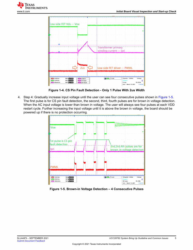
Figure 1-4. CS Pin Fault Detection - Only 1 Pulse With 2us Width
4. Step 4: Gradually increase input voltage until the user can see four consecutive pulses shown in Figure 1-5. The first pulse is for CS pin fault detection, the second, third, fourth pulses are for brown in voltage detection. When the AC input voltage is lower than brown in voltage. The user will always see four pulses at each VDD restart cycle. Further increasing the input voltage until it is above the brown in voltage, the board should be powered up if there is no protection occurring.
Figure 1-5. Brown-in Voltage Detection – 4 Consecutive Pulses
www.ti.com Initial Board Visual Inspection and Start-up Check
SLUAAF9 – SEPTEMBER 2021Submit Document Feedback
UCC28782 System Bring Up Guideline and Common Issues 5
Copyright © 2021 Texas Instruments Incorporated

2 Typical System Operating WaveformsUCC28782 contains six modes of operation that summarized in UCC28782 data sheet Table 8-1. From no load to full load, the operation modes include Survival Mode, SBP2(Second StandBy Power Mode), SBP1, (First StandBy Power Mode) LPM (Low Power Mode), ABM (Adaptive Burst Mode), AAM (Adaptive Amplitude Modulation), The survival mode only kicks in when VDD voltage lower than the 13-V survival mode threshold and also performs the clamping capacitor balancing function to reduce the voltage stress of the secondary side rectifier. Typically, the system does not enter survival mode during regular load change, such as smooth load increase and decrease. The survival mode might kick in at a large output load remove, overshoot on output results in controller stop switching in a long time, then the VDD voltage might drop to touch the 13-V survival mode threshold. The following waveforms show each mode operation (no load to full load).
2.1 SBP2 ModeAt no load or very light load, PWMH is disabled and there are four PWML pulses in each burst packet. The peak current of each pulse is programmable through the resistance from IPC pin to ground. See Figure 2-1.
Figure 2-1. SBP2 Mode Operation Waveform
2.2 SBP1 ModeGradually increase load at SBP2 mode, the system will entry SBP1 mode, PWMH is still disabled and there are two PWML pulses in each burst packet. The peak current is fixed and this is determined by VCST(MIN). Burst frequency is less than 25 khz and it is variable based on the load. As shown in Figure 2-2.
Typical System Operating Waveforms www.ti.com
6 UCC28782 System Bring Up Guideline and Common Issues SLUAAF9 – SEPTEMBER 2021Submit Document Feedback
Copyright © 2021 Texas Instruments Incorporated

Figure 2-2. SBP1 Mode Operation Waveform
2.3 LPM modeGradually increase load at SBP1 mode, the system will enter LPM mode, PWMH is disabled and there are two PWML pulses in each burst packet. But, the peak current is variable, as VCST will vary from VCST(MIN) to VCST(BUR). The burst frequency is fixed at 25 khz. See Figure 2-3.
Figure 2-3. LPM Mode Operation Waveform
2.4 LPM to ABM Mode TransitionAs load increases, VCST reaches VCST(BUR), LPM mode transient to ABM, PWMH is enabled at ABM. A large negative current for example, balancing current can be observed when the first PWMH is enabled as shown in Figure 2-4.
www.ti.com Typical System Operating Waveforms
SLUAAF9 – SEPTEMBER 2021Submit Document Feedback
UCC28782 System Bring Up Guideline and Common Issues 7
Copyright © 2021 Texas Instruments Incorporated

Figure 2-4. LPM to ABM Mode Transition
2.5 ABM ModeAt ABM mode, the peak current is clamped at VCST(BUR)/Rcs, PWMH is enabled, so Zero-Voltage Switching (ZVS) is achieved except for the first switching cycle. The number of PWML pulses (NSW) is modulated to ensure burst frequency stays above 25khz. As load increases, burst frequency becomes higher and reaches to the high-level burst frequency threshold fBUR(UP), the ABM loop commands NSW to be increased by one pulse to push burst frequency fBUR below fBUR(UP). Additional details can be found in UCC28782 data sheet section 8.4.6.
Figure 2-5. ABM Mode PWML Pulse NSW=2
Typical System Operating Waveforms www.ti.com
8 UCC28782 System Bring Up Guideline and Common Issues SLUAAF9 – SEPTEMBER 2021Submit Document Feedback
Copyright © 2021 Texas Instruments Incorporated

Figure 2-6. ABM Mode PWML Pulse NSW=7
2.6 ABM to AAM Mode TransitionFigure 2-7 demonstrates ABM transition to AAM. As load is closed to the boundary of ABM and AAM, the two adjacent burst packets with the maximum pulse count can stat to bundle together. To mitigate the output ripple and audible noise concerns, when the bundled burst packet appears two times with eight sequential burst cycles, the controller will reduce VBUR. The less energy per cycle with a lower VBUR will force the control loop to transition from ABM to AAM smoothly.
Figure 2-7. ABM to AAM Mode Transition
2.7 AAM ModeAt AAM mode Figure 2-8, PWML and PWMH alternate turn on in a complementary fashion with dead-time in between, as load current increases Figure 2-9, peak current increases while the switching frequency decreases.
www.ti.com Typical System Operating Waveforms
SLUAAF9 – SEPTEMBER 2021Submit Document Feedback
UCC28782 System Bring Up Guideline and Common Issues 9
Copyright © 2021 Texas Instruments Incorporated

Figure 2-8. AAM Mode Medium Load
Figure 2-9. AAM Mode Heavy Load
Typical System Operating Waveforms www.ti.com
10 UCC28782 System Bring Up Guideline and Common Issues SLUAAF9 – SEPTEMBER 2021Submit Document Feedback
Copyright © 2021 Texas Instruments Incorporated

3 Typical System Protection WaveformsThe UCC28782 provides extensive protections on different system fault scenarios for robust operation. All system protection features are summarized in UCC28782 data sheet Table 8-3, and the pin fault protections are summarized in the data sheet Table 8-4. If the input voltage is higher than brown_in voltage, but output voltage cannot be regulated, there is a high chance that some protections might be triggered, this section describes some typical system protections.
3.1 Over-Power Protection (OPP)The two key things used to identify what protection happens on the board are delay to action and action, which also listed in UCC28782 data sheet Table 8-3, for OPP, delay to action shown in Figure 3-1is VCST ≥ VCST(OPP) and maintain above 160ms, action shown in Figure 3-2is tFDR restart(1.5s).
Figure 3-1. OPP Delay to Action
Figure 3-2. OPP Action
CH3: Low side FET Vds (Vsw), CH4: Transformer primary winding current (Ipri), CH2: Output voltage (Vout).
www.ti.com Typical System Protection Waveforms
SLUAAF9 – SEPTEMBER 2021Submit Document Feedback
UCC28782 System Bring Up Guideline and Common Issues 11
Copyright © 2021 Texas Instruments Incorporated

3.2 Output Overvoltage Protection (OVP)Output voltage is detected by controller through VS pin, However, it is not recommended to probe VS pin directly as the noise introduced by probing could cause protection mis-triggering. Instead, AUX winding voltage can be used for identifying whether OVP happens. If the divided voltage on VS pin exceed OVP threshold for three consecutive pulses, OVP is triggered.
Figure 3-3. OVP Delay to Action
Figure 3-4. OVP Delay to Action (Zoom In)
Typical System Protection Waveforms www.ti.com
12 UCC28782 System Bring Up Guideline and Common Issues SLUAAF9 – SEPTEMBER 2021Submit Document Feedback
Copyright © 2021 Texas Instruments Incorporated
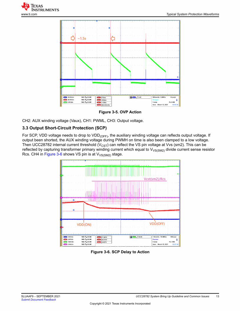
Figure 3-5. OVP Action
CH2: AUX winding voltage (Vaux), CH1: PWML, CH3: Output voltage.
3.3 Output Short-Circuit Protection (SCP)For SCP, VDD voltage needs to drop to VDD(OFF), the auxiliary winding voltage can reflects output voltage. If output been shorted, the AUX winding voltage during PWMH on time is also been clamped to a low voltage. Then UCC28782 internal current threshold (VCST) can reflect the VS pin voltage at Vvs (sm2). This can be reflected by capturing transformer primary winding current which equal to VVS(SM2) divide current sense resistor Rcs. CH4 in Figure 3-6 shows VS pin is at VVS(SM2) stage.
Figure 3-6. SCP Delay to Action
www.ti.com Typical System Protection Waveforms
SLUAAF9 – SEPTEMBER 2021Submit Document Feedback
UCC28782 System Bring Up Guideline and Common Issues 13
Copyright © 2021 Texas Instruments Incorporated

Figure 3-7. SCP Action
CH3: Low side FET Vds, CH4: Primary current, CH2: VDD
Additional protections details and corresponding solutions can be found in Debugging UCC28780 ACF Converter Start-up Issues. application note.
Typical System Protection Waveforms www.ti.com
14 UCC28782 System Bring Up Guideline and Common Issues SLUAAF9 – SEPTEMBER 2021Submit Document Feedback
Copyright © 2021 Texas Instruments Incorporated

4 Common Issues and SolutionsThis section covers some common issues that a designer might face during the board debug stage and corresponding solutions are presented. The following three subsections covers regulation, light load, and transient conditions.
4.1 VDD Boost Converter Survival Mode
4.1.1 Survival Mode Due To Boost Inductor DCR Too High.
UCC28782 integrates a boost converter to supply VDD in a wide output voltage range application, such as USB PD charger. The typical UVLO threshold of boost converter is 1.23 V, If BIN capacitors are occasionally completely discharged, shown in Figure 4-1, resulting in additional power losses, irregular operation and higher output ripple, this could be caused by boost inductor DCR too high which results in VBIN UVLO not proper been detected (UVLO off threshold of VBIN is around 1.23V, large DCR of boost inductor will lead to VBIN always higher than 1.23 V during boost Mosfet turn on time.). The boost converter always turns on until the energy on BIN capacitors be consumed up.
Figure 4-1. Boost Inductor DCR > 1 ohm
Figure 4-2. Boost Inductor DCR = 0.56 ohm
Solution: Choose the boost inductor with DCR less than 1 ohm. 0.5 ohm ~0.7 ohm is preferred.
4.1.2 System Stays In Survival Mode When the Output Voltage is Low Such as 3.3V/5V/9V
If this occurs, it might be due to BIN and VDD capacitance are too small. At no load, energy in each survival mode pulse is intended to go to BIN and VDD networks on the primary side of transformer. If the auxiliary winding resistance RAUX is high, it can be difficult to pass this energy to BIN capacitors, and most of the energy
www.ti.com Common Issues and Solutions
SLUAAF9 – SEPTEMBER 2021Submit Document Feedback
UCC28782 System Bring Up Guideline and Common Issues 15
Copyright © 2021 Texas Instruments Incorporated

goes to output instead. This results in more survival mode pulses than expected to get energy into BIN and VDD which overcharges Vout.
Solution: Use higher BIN and VDD capacitance to attract energy to AUX side. ~47 uF on BIN and ~22 uF on VDD is a good start.
Higher capacitors at BIN pin CBIN keeps BIN voltage lower than reflected Vout so pulse current steers to BIN instead of Vout. Higher CVDD keeps VDD higher so fewer survival mode pulses are required. Low RAUX allows survival mode pulse energy to steer easily in to lower-value BIN cap.
4.2 10% Load Efficiency Might not Meet spec. in USB-PD Application, Especially at 5 V/9 V Output ConditionThe result could be caused by improper current sense resistor Rcs setting and not using the IPC pin resistor. This process results in a higher burst switching frequency. At 10% load the switching losses become dominant, reduce switching frequency helps reduce switching losses and improve efficiency.
Figure 4-3. Operating at SBP1 Mode
Figure 4-4. Operating at SBP2 Mode
Solution:
1. Reduce current resistor Rcs and increase CS pin filter capacitor Ccs to push operation mode from SBP1 into SBP2.
Figure 4-3 shows the waveform of SBP1 operation, Figure 4-4 shows the waveform after reducing Rcs or increase Ccs to push Fsw<8 kHz. this helps the system operates at SBP2 mode and improve efficiency significantly.
2. Add a resistor between IPC and AGND
Common Issues and Solutions www.ti.com
16 UCC28782 System Bring Up Guideline and Common Issues SLUAAF9 – SEPTEMBER 2021Submit Document Feedback
Copyright © 2021 Texas Instruments Incorporated

Disconnecting a resistor from IPC to AGND is not a mandatory requirement, but connecting a resistor in here helps for improving the light load efficiency especially when 5 V/9 V can’t meet the average efficiency spec.
VIPC
VCST
VCST_IPC(LR)
VCST_IPC(MIN)
0.9V
VCST_IPC(UP)
0.15V
0.27V
0.4V
1.8V 3.8V 5V0V
Figure 4-5. IPC Pin Resistor Setting
There is a 50 uA current source out of the IPC pin, the voltage on IPC pin resistor (VIPC)can program the peak current threshold (VCST_IPC) at SBP2 mode. Higher peak current can further reduce fsw then improve 10% load efficiency, but higher peak current may cause audible noise, trade off between efficiency and noise level maybe need to be made.
4.3 Transient
4.3.1 BIN/BSW Pin Damage During LPM to ABM Mode Transition
This transition could be caused by RDM or BUR pin resistor not selected properly. When the power stage running at LPM mode, high-side driver PWMH is disabled, transformer leakage energy will be accumulated at clamp capacitors while results in voltage on clamp capacitors slightly higher than output reflected voltage, as load increasing, power stage will transfer from LPM to ABM mode, there is a large balancing current between clamp capacitors and output capacitors when the first PWMH enabled, if PWMH on time is shorten than the resonance time of leakage inductance and clamp capacitors. NON-ZCS turn off will happen as shown in Figure 4-6, A sharp di/dt on leakage inductance causes high voltage spike which coupling to AUX winding, there is a potential risk that damage BIN/BSW pins, and SR FET also shows over voltage stress at this moment.
Figure 4-6. SR FET Non-ZCS Turn Off
www.ti.com Common Issues and Solutions
SLUAAF9 – SEPTEMBER 2021Submit Document Feedback
UCC28782 System Bring Up Guideline and Common Issues 17
Copyright © 2021 Texas Instruments Incorporated

Figure 4-7. SR FET ZCS Turn Off
Solution:
1. Re-calculate RDM pin resistor value,The RRDM calculation equation shown in UCC28782 data sheet equation (11). If the actual value on the tested board is close to calculated value, minor increase RDM resistor until the user can see NON-ZCS turn off disappear, see Figure 4-7
2. Decrease down-side resistor value of BUR pin divider. So the peak current at LPM is reduced, in this way, the energy stored in clamp capacitors is also reduced. This process will assist for smaller balancing current.
4.3.2 SR MOSFET VDS Overstress at Survival Mode
This process could rarely be observed at full load transient to no load, output voltage overshoot results in UCC28782 long time pulse stop, shown in Figure 4-8.VDD drop to around 13-V due to the controller still consume the energy on VDD capacitances even pulse is stopped. While BIN capacitors been over discharged during this time. When survival mode kicks in, most of current flow into BIN pin caps, less current go to SR FET, SR turn on at minimum on time that a reverse current can be seen at it’s turn off edge. This reverse current will trigger next turn on pulse that lead to SR turn on again and again.
Figure 4-8. SR Vds Overstress When Survival Mode Kick In
Common Issues and Solutions www.ti.com
18 UCC28782 System Bring Up Guideline and Common Issues SLUAAF9 – SEPTEMBER 2021Submit Document Feedback
Copyright © 2021 Texas Instruments Incorporated
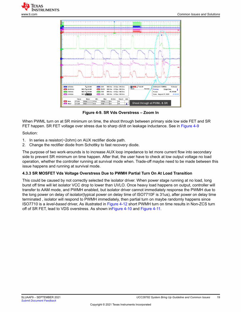
Figure 4-9. SR Vds Overstress – Zoom In
When PWML turn on at SR minimum on time, the shoot through between primary side low side FET and SR FET happen. SR FET voltage over stress due to sharp di/dt on leakage inductance. See in Figure 4-9
Solution:
1. In series a resistor(~2ohm) on AUX rectifier diode path.2. Change the rectifier diode from Schottky to fast recovery diode.
The purpose of two work-arounds is to increase AUX loop impedance to let more current flow into secondary side to prevent SR minimum on time happen. After that, the user have to check at low output voltage no load operation, whether the controller running at survival mode when. Trade-off maybe need to be made between this issue happens and running at survival mode.
4.3.3 SR MOSFET Vds Voltage Overstress Due to PWMH Partial Turn On At Load Transition
This could be caused by not correctly selected the isolator driver. When power stage running at no load, long burst off time will let isolator VCC drop to lower than UVLO. Once heavy load happens on output, controller will transfer to AAM mode, and PWMH enabled, but isolator driver cannot immediately response the PWMH due to the long power on delay of isolator(typical power on delay time of ISO7710F is 31us), after power on delay time terminated , isolator will respond to PWMH immediately, then partial turn on maybe randomly happens since ISO7710 is a level-based driver, As illustrated in Figure 4-12 short PWMH turn on time results in Non-ZCS turn off of SR FET, lead to VDS overstress. As shown inFigure 4-10 and Figure 4-11.
www.ti.com Common Issues and Solutions
SLUAAF9 – SEPTEMBER 2021Submit Document Feedback
UCC28782 System Bring Up Guideline and Common Issues 19
Copyright © 2021 Texas Instruments Incorporated

Figure 4-10. PWMH Partial Turn On
Figure 4-11. PWMH Partial Turn On – Zoom In
Solution:
Change isolator driver from level-based driver to edge-based driver Figure 4-13, such as ISO7310, it can prevent partial response to PWMH. Then SR is able to ZCS turn off to avoiding over stress. After change to ISO7310, The waveforms shown in Figure 4-14.
Common Issues and Solutions www.ti.com
20 UCC28782 System Bring Up Guideline and Common Issues SLUAAF9 – SEPTEMBER 2021Submit Document Feedback
Copyright © 2021 Texas Instruments Incorporated

TX IN
RX OUT
Signal through
isolation barrier
ISO7710
Figure 4-12. Level Based Isolation Driver Architecture
OSC
PWM
LPF
VREF
DCL
OUT
IN
0
1 S
Isolation Barrier
Low-Frequency
Channel
(DC...100 kbps)
High-Frequency
Channel
(100 kbps...150 Mbps)
VREF
TXP
TXN
RXP
RXN
ISO7310
Figure 4-13. Edge Based Isolation Driver Architecture
www.ti.com Common Issues and Solutions
SLUAAF9 – SEPTEMBER 2021Submit Document Feedback
UCC28782 System Bring Up Guideline and Common Issues 21
Copyright © 2021 Texas Instruments Incorporated

Figure 4-14. Isolator Change to ISO7310
Common Issues and Solutions www.ti.com
22 UCC28782 System Bring Up Guideline and Common Issues SLUAAF9 – SEPTEMBER 2021Submit Document Feedback
Copyright © 2021 Texas Instruments Incorporated
5 References1. Texas Instruments, UCC28782 High Density Active Clamp Flyback Controller with EMI Dithering, X-Cap
Discharge, and Bias Power Management data sheet.2. Texas Instruments, Debugging UCC28780 ACF Converter Start-up Issues application note.3. Texas Instruments, Using the UCC28782EVM-030 65-W USB-C PD High-Density Active-Clamp Flyback
Converter user guide.
www.ti.com References
SLUAAF9 – SEPTEMBER 2021Submit Document Feedback
UCC28782 System Bring Up Guideline and Common Issues 23
Copyright © 2021 Texas Instruments Incorporated

IMPORTANT NOTICE AND DISCLAIMERTI PROVIDES TECHNICAL AND RELIABILITY DATA (INCLUDING DATASHEETS), DESIGN RESOURCES (INCLUDING REFERENCEDESIGNS), APPLICATION OR OTHER DESIGN ADVICE, WEB TOOLS, SAFETY INFORMATION, AND OTHER RESOURCES “AS IS”AND WITH ALL FAULTS, AND DISCLAIMS ALL WARRANTIES, EXPRESS AND IMPLIED, INCLUDING WITHOUT LIMITATION ANYIMPLIED WARRANTIES OF MERCHANTABILITY, FITNESS FOR A PARTICULAR PURPOSE OR NON-INFRINGEMENT OF THIRDPARTY INTELLECTUAL PROPERTY RIGHTS.These resources are intended for skilled developers designing with TI products. You are solely responsible for (1) selecting the appropriateTI products for your application, (2) designing, validating and testing your application, and (3) ensuring your application meets applicablestandards, and any other safety, security, or other requirements. These resources are subject to change without notice. TI grants youpermission to use these resources only for development of an application that uses the TI products described in the resource. Otherreproduction and display of these resources is prohibited. No license is granted to any other TI intellectual property right or to any third partyintellectual property right. TI disclaims responsibility for, and you will fully indemnify TI and its representatives against, any claims, damages,costs, losses, and liabilities arising out of your use of these resources.TI’s products are provided subject to TI’s Terms of Sale (https:www.ti.com/legal/termsofsale.html) or other applicable terms available eitheron ti.com or provided in conjunction with such TI products. TI’s provision of these resources does not expand or otherwise alter TI’sapplicable warranties or warranty disclaimers for TI products.IMPORTANT NOTICE
Mailing Address: Texas Instruments, Post Office Box 655303, Dallas, Texas 75265Copyright © 2021, Texas Instruments Incorporated