ucc28700-q1 - texas instruments · ucc28700-q1 slusc61 –january 2015 6 specifications 6.1...
TRANSCRIPT

D2
RCS
+±
DRV
CS
CDD
VDD
GND
RS1
RS2
VS
Np Ns
Na
RSTR
VAUX
VAC
CBC RLC
UCC28700-Q1SOT23-6
COUTVOUTNs RPL
VREG
CB2
VBLK
CB1
RCBC
D1
Product
Folder
Sample &Buy
Technical
Documents
Tools &
Software
Support &Community
ReferenceDesign
UCC28700-Q1SLUSC61 –JANUARY 2015
UCC28700-Q1 Constant-Voltage, Constant-Current ControllerWith Primary-Side Regulation
1 Features 3 DescriptionThe UCC28700-Q1 of flyback power supply
1• Qualified for Automotive Applicationscontrollers provides Constant-Voltage (CV) and• AEC-Q100 Qualified with the Following Results: Constant-Current (CC) output regulation without the
– Device Temperature Grade 1: –40°C to 125°C use of an optical coupler. The devices processinformation from the primary power switch and an– Device HBM Classification Level 2: ±2 kVauxiliary flyback winding for precise control of output– Device CDM Classification Level C4B: 750 V voltage and current. Low start-up current, dynamically
• < 30-mW Standby Power Consumption controlled operating states and a tailored modulationprofile support very low standby power without• Primary-Side Regulation (PSR) Eliminates Opto-sacrificing start-up time or output transient response.Coupler
• ±5% Voltage and Current Regulation Control algorithms in the UCC28700-Q1 allowsoperating efficiencies to meet or exceed applicable• 130-kHz Maximum Switching Frequencystandards. The output drive interfaces to a MOSFET• Quasi-Resonant Valley-Switching Operation for power switch. Discontinuous Conduction ModeHighest Overall Efficiency (DCM) with valley switching reduces switching losses.
• Patent-Pending Frequency-Jitter Scheme to Ease Modulation of switching frequency and primaryEMI Compliance current peak amplitude (FM and AM) keeps the
conversion efficiency high across the entire load and• Wide VDD Range Allows Small Bias Capacitorline ranges.• Clamped Gate-Drive Output for MOSFETThe controllers have a maximum switching frequency• Protection Functions: Overvoltage, Low-Line, andof 130 kHz and always maintain control of the peak-Overcurrent primary current in the transformer. Protection features
• Programmable Cable Compensation help keep primary and secondary component• SOT23-6 Package stresses in check. The UCC28700-Q1 allows the
level of cable compensation to be programmed.2 Applications
Device Information(1)• Automotive AC-to-DC and DC-to-DC Power
PART NUMBER PACKAGE BODY SIZE (NOM)ConversionUCC28700-Q1 SOT-23 (6) 2.90 mm × 1.60 mm
• Auxiliary Power Supply for Automotive Power(1) For all available packages, see the orderable addendum atTrain in HEV
the end of the datasheet.• Flyback and Buck Power Converters
Typical Application Schematic
1
An IMPORTANT NOTICE at the end of this data sheet addresses availability, warranty, changes, use in safety-critical applications,intellectual property matters and other important disclaimers. PRODUCTION DATA.

UCC28700-Q1SLUSC61 –JANUARY 2015 www.ti.com
Table of Contents7.3 Feature Description................................................. 101 Features .................................................................. 17.4 Device Functional Modes........................................ 132 Applications ........................................................... 1
8 Applications and Implementation ...................... 173 Description ............................................................. 18.1 Application Information............................................ 174 Revision History..................................................... 28.2 Typical Application .................................................. 175 Pin Configuration and Functions ......................... 3
9 Power Supply Recommendations ...................... 266 Specifications......................................................... 410 Layout................................................................... 266.1 Absolute Maximum Ratings ...................................... 4
10.1 Layout Guidelines ................................................. 266.2 ESD Ratings ............................................................ 410.2 Layout Example .................................................... 276.3 Recommended Operating Conditions....................... 4
11 Device and Documentation Support ................. 286.4 Thermal Information .................................................. 511.1 Device Support...................................................... 286.5 Electrical Characteristics........................................... 511.2 Documentation Support ........................................ 316.6 Switching Characteristics .......................................... 611.3 Trademarks ........................................................... 316.7 Typical Characteristics .............................................. 711.4 Electrostatic Discharge Caution............................ 317 Detailed Description .............................................. 9
12 Mechanical, Packaging, and Orderable7.1 Overview ................................................................... 9Information ........................................................... 317.2 Functional Block Diagram ......................................... 9
4 Revision History
DATE REVISION NOTESJanuary 2015 * Initial release.
2 Submit Documentation Feedback Copyright © 2015, Texas Instruments Incorporated
Product Folder Links: UCC28700-Q1

1
2
3
6
5
4
VDD
DRV
VS
GND
CS
CBC
UCC28700-Q1www.ti.com SLUSC61 –JANUARY 2015
5 Pin Configuration and Functions
UCC28700-Q1SOT23-6 (DBV)
Top View
Pin FunctionsPIN
UCC28700-Q1 I/O DESCRIPTIONNAME
NO.Cable Compensation (CBC) is a programming pin for compensation of cable voltageCBC 1 I drop. Cable compensation is programmed with a resistor to GND.Current Sense (CS) input connects to a ground-referenced current-sense resistor inseries with the power switch. The resulting voltage is used to monitor and control theCS 4 I peak primary current. A series resistor can be added to this pin to compensate the peakswitch current levels as the AC-mains input varies.Drive (DRV) is an output used to drive the gate of an external high voltage MOSFETDRV 3 O switching transistor.The Ground (GND) pin is both the reference pin for the controller and the low-side returnfor the drive output. Special care should be taken to return all AC decoupling capacitorsGND 5 — as close as possible to this pin and avoid any common trace length with analog signalreturn paths.VDD is the bias supply input pin to the controller. A carefully-placed bypass capacitor toVDD 2 — GND is required on this pin.Voltage Sense (VS) is an input used to provide voltage and timing feedback to thecontroller. This pin is connected to a voltage divider between an auxiliary winding andVS 6 I GND. The value of the upper resistor of this divider is used to program the AC-mains runand stop thresholds and line compensation at the CS pin.
Copyright © 2015, Texas Instruments Incorporated Submit Documentation Feedback 3
Product Folder Links: UCC28700-Q1

UCC28700-Q1SLUSC61 –JANUARY 2015 www.ti.com
6 Specifications
6.1 Absolute Maximum Ratings (1)
over operating free-air temperature range (unless otherwise noted)MIN MAX UNIT
Bias supply voltage VVDD 38 VContinuous gate current sink IDRV 50
Self-Continuous gate current source IDRV mAlimitingPeak VS pin current IVS −1.2
Self-Gate-drive voltage at DRV VDRV −0.5 limitingVVS −0.75 7
Voltage rangeCS, CBC −0.5 5
Operating junction temperature range TJ −55 150°C
Lead temperature 0.6 mm from case for 10 seconds 260Storage temperature, Tstg –65 150 °C
(1) Stresses beyond those listed under Absolute Maximum Ratings may cause permanent damage to the device. These are stress ratingsonly and functional operation of the device at these or any other conditions beyond those indicated under Recommended OperatingConditions is not implied. Exposure to absolute-maximum-rated conditions for extended periods may affect device reliability. All voltagesare with respect to GND. Currents are positive into, negative out of the specified terminal. These ratings apply over the operatingambient temperature ranges unless otherwise noted.
6.2 ESD RatingsVALUE UNIT
Human-body model (HBM), per AEC Q100-002 (1) ±2000V(ESD) Electrostatic discharge V
Charged-device model (CDM), per AEC Q100-011 ±750
(1) AEC Q100-002 indicates that HBM stressing shall be in accordance with the ANSI/ESDA/JEDEC JS-001 specification.
6.3 Recommended Operating Conditionsover operating free-air temperature range (unless otherwise noted)
MIN MAX UNITVDD Bias supply operating voltage 9 35 VCVDD VDD bypass capacitor 0.047 1 µFRCBC Cable-compensation resistance 10 kΩIVS VS pin current −1 mATJ Operating junction temperature −40 125 °C
4 Submit Documentation Feedback Copyright © 2015, Texas Instruments Incorporated
Product Folder Links: UCC28700-Q1

UCC28700-Q1www.ti.com SLUSC61 –JANUARY 2015
6.4 Thermal InformationUCC28700-Q1
THERMAL METRIC (1) DBV UNIT6 PINS
θJA Junction-to-ambient thermal resistance (2) 180θJCtop Junction-to-case (top) thermal resistance (3) 71.2θJB Junction-to-board thermal resistance (4) 44.4 °C/WψJT Junction-to-top characterization parameter (5) 5.1ψJB Junction-to-board characterization parameter (6) 43.8
(1) For more information about traditional and new thermal metrics, see the IC Package Thermal Metrics application report, SPRA953.(2) The junction-to-ambient thermal resistance under natural convection is obtained in a simulation on a JEDEC-standard, high-K board, as
specified in JESD51-7, in an environment described in JESD51-2a.(3) The junction-to-case (top) thermal resistance is obtained by simulating a cold plate test on the package top. No specific JEDEC-
standard test exists, but a close description can be found in the ANSI SEMI standard G30-88.(4) The junction-to-board thermal resistance is obtained by simulating in an environment with a ring cold plate fixture to control the PCB
temperature, as described in JESD51-8.(5) The junction-to-top characterization parameter, ψJT, estimates the junction temperature of a device in a real system and is extracted
from the simulation data for obtaining RθJA, using a procedure described in JESD51-2a (sections 6 and 7).(6) The junction-to-board characterization parameter, ψJB, estimates the junction temperature of a device in a real system and is extracted
from the simulation data for obtaining RθJA, using a procedure described in JESD51-2a (sections 6 and 7).
6.5 Electrical Characteristicsover operating free-air temperature range, VDD = 25 V, RCBC = open, –40°C ≤ TA ≤ 125°C, TJ = TA(unless otherwise noted)
PARAMETER TEST CONDITIONS MIN TYP MAX UNITSBIAS SUPPLY INPUTIRUN Supply current, run IDRV = 0, run state 2.10 2.65 mAIWAIT Supply current, wait IDRV = 0, wait state 85 110
µAISTART Supply current, start IDRV = 0, VVDD = 18 V, start state 1.0 1.5IFAULT Supply current, fault IDRV = 0, fault state 2.1 2.8 mAUNDER-VOLTAGE LOCKOUTVVDD(on) VDD turn-on threshold VVDD low to high 17.5 21.0 23.0
VVVDD(off) VDD turn-off threshold VVDD high to low 7.70 8.10 8.45VS INPUTVVSR Regulating level Measured at no-load condition, TJ = 25°C 4.01 4.05 4.09 VVVSNC Negative clamp level IVS = -300 µA, volts below ground 190 250 325 mVIVSB Input bias current VVS = 4 V –0.25 0 0.25 µACS INPUTVCST(max) Max CS threshold voltage VVS = 3.7 V (1) 715 750 775
mVVCST(min) Min CS threshold voltage VVS = 4.35 V (1) 230 250 270KAM AM control ratio VCST(max) / VCST(min) 2.75 3.00 3.15 V/V
constant-current regulatingVCCR CC regulation constant 310 319 329 mVlevelLine compensating currentKLC IVSLS = -300 µA, IVSLS / current out of CS pin 23 25 28 A/Aratio
TCSLEB Leading-edge blanking time DRV output duration, VCS = 1 V 195 235 275 nsDRVIDRS DRV source current VDRV = 8 V, VVDD = 9 V 20 25 mARDRVLS DRV low-side drive resistance IDRV = 10 mA 6 12 ΩVDRCL DRV clamp voltage VVDD = 35 V 14 16 VRDRVSS DRV pull-down in start state 150 200 230 kΩ
(1) These devices automatically vary the control frequency and current sense thresholds to improve EMI performance, these thresholdvoltages and frequency limits represent average levels.
Copyright © 2015, Texas Instruments Incorporated Submit Documentation Feedback 5
Product Folder Links: UCC28700-Q1

UCC28700-Q1SLUSC61 –JANUARY 2015 www.ti.com
Electrical Characteristics (continued)over operating free-air temperature range, VDD = 25 V, RCBC = open, –40°C ≤ TA ≤ 125°C, TJ = TA(unless otherwise noted)
PARAMETER TEST CONDITIONS MIN TYP MAX UNITSPROTECTIONVOVP Over-voltage threshold At VS input, TJ = 25°C 4.52 4.60 4.68
VVOCP Over-current threshold At CS input 1.4 1.5 1.6IVSL(run) VS line-sense run current Current out of VS pin – increasing 190 220 260
µAIVSL(stop) VS line-sense stop current Current out of VS pin – decreasing 70 80 95KVSL VS line-sense ratio IVSL(run) / IVSL(stop) 2.50 2.80 3.05 A/A
Thermal shut-downTJ(stop) Internal junction temperature 165 °CtemperatureCABLE COMPENSATION
Cable compensationVCBC(max) Voltage at CBC at full load 2.8 3.0 3.4 Vmaximum voltageVCBC = open, change in VS regulating level at fullVCVS(min) Compensation at VS –45 –15 25load
mVMaximum compensation at VCBC = 0 V, change in VS regulating level at fullVCVS(max) 275 320 365VS load
6.6 Switching Characteristicsover operating free-air temperature range (unless otherwise noted)
PARAMETER TEST CONDITIONS MIN TYP MAX UNITfSW(max) Maximum switching frequency VVS = 3.7 V (1) 120 130 140 kHzfSW(min) Minimum switching frequency VVS = 4.35 V (1) 875 1000 1100 HzTZTO Zero-crossing timeout delay 1.80 2.10 2.55 µs
(1) These devices automatically vary the control frequency and current sense thresholds to improve EMI performance, these thresholdvoltages and frequency limits represent average levels.
6 Submit Documentation Feedback Copyright © 2015, Texas Instruments Incorporated
Product Folder Links: UCC28700-Q1

230
235
240
245
250
255
260
265
270
−25 0 25 50 75 100 125TJ − Temperature (°C)
VC
ST
MIN
− M
inim
um C
S T
hres
hold
Vol
tage
(m
V)
G005
310
315
320
325
330
−25 0 25 50 75 100 125TJ − Temperature (°C)
VC
CR −
Con
stan
t Cur
rent
Reg
ulat
ing
Leve
l (m
V)
G006
3.96
3.98
4.00
4.02
4.04
4.06
4.08
4.10
−25 0 25 50 75 100 125TJ − Temperature (°C)
VV
SR −
VS
Reg
ulat
ion
Vol
tage
(V
)
G003
0
50
100
150
200
250
300
−20 5 30 55 80 105 125TJ − Temperature (°C)
VS
Lin
e S
ense
Cur
rent
(µA
)IVSLRUN
IVSLSTOP
G004
0.00001
0.0001
0.001
0.01
0.1
1
10
0 5 10 15 20 25 30 35
VDD Turn−Off VDD Turn−On
VDD − Bias Supply Voltage (V)
I VD
D −
Bia
s S
uppl
y C
urre
nt (
mA
)
Run State
Wait State
Start State
G001
0.0001
0.001
0.01
0.1
1
10
−25 0 25 50 75 100 125TJ − Temperature (°C)
I VD
D −
Bia
s S
uppl
y C
urre
nt (
mA
)
IRUN, VDD = 25 V
IWAIT, VDD = 25 V
ISTART, VDD = 18 V
G002
UCC28700-Q1www.ti.com SLUSC61 –JANUARY 2015
6.7 Typical CharacteristicsAt VDD = 25 V, unless otherwise noted.
Figure 1. Bias Supply Current vs. Bias Supply Voltage Figure 2. Bias Supply Current vs. Temperature
Figure 3. VS Regulation Voltage vs. Temperature Figure 4. Line-Sense Current vs. Temperature
Figure 5. Minimum CS Threshold Voltage vs. Temperature Figure 6. Constant-Current Regulating Level vs.Temperature
Copyright © 2015, Texas Instruments Incorporated Submit Documentation Feedback 7
Product Folder Links: UCC28700-Q1

4.52
4.54
4.56
4.58
4.60
4.62
4.64
4.66
4.68
−25 0 25 50 75 100 125TJ − Temperature (°C)
VO
VP −
VS
Ove
r−V
olta
ge T
hres
hold
(V
)
G011
875
900
925
950
975
1000
1025
1050
1075
1100
−25 0 25 50 75 100 125TJ − Temperature (°C)
FS
WM
IN −
Min
imum
Sw
itchi
ng F
requ
ency
(H
z)
G007
UCC28700-Q1SLUSC61 –JANUARY 2015 www.ti.com
Typical Characteristics (continued)At VDD = 25 V, unless otherwise noted.
VDRV = 8 V, VVDD = 9 V
Figure 7. Minimum Switching Frequency vs. Temperature Figure 8. DRV Source Current vs. Temperature
Figure 9. Overvoltage Threshold vs. Temperature
8 Submit Documentation Feedback Copyright © 2015, Texas Instruments Incorporated
Product Folder Links: UCC28700-Q1

DRV
25mA
S Q
QR
CS+
VS SAMPLER
+E/A
4V + VCVS
CBC
VDD
POWER& FAULT
MANAGEMENT
UVLO21V/8V
VALLEY SWITCHING
CONTROLLAW
LEB
1/FSWVCST
STARTRUNWAITFAULT
SECONDARYTIMINGDETECT
CURRENTREGULATION
VCST
200K
VDD
LINE SENSE
+
VSS
ICBC
0V-3V
GND
CABLECOMPENSATION
VCVS
+
VOVPOV FAULT
OV FAULTTSD/SD FAULT
IVSLS
+10k LINE FAULT
LINE FAULT
14V
2.1V / 0.75V
+
1.5V
OC FAULT
OC FAULT
IVSLS / KLCIVSLS
28 k:
UCC28700-Q1www.ti.com SLUSC61 –JANUARY 2015
7 Detailed Description
7.1 OverviewThe UCC28700-Q1 is a flyback power supply controller which provides accurate voltage and constant currentregulation with primary-side feedback, eliminating the need for opto-coupler feedback circuits. The controlleroperates in discontinuous conduction mode with valley-switching to minimize switching losses. The modulationscheme is a combination of frequency and primary peak current modulation to provide high conversion efficiencyacross the load range. The control law provides a wide-dynamic operating range of output power to achieve the<30-mW stand-by power requirement.
Another feature beneficial to achieve low stand-by power without excessive start-up time is a wide operatingVDD range to allow a high-value VDD start-up resistance and low-value VDD capacitance. During low-poweroperating ranges the device has power management features to reduce the device operating current at operatingfrequencies below 44 kHz. The UCC28700-Q1 controller includes features in the modulator to reduce the EMIpeak energy of the fundamental switching frequency and harmonics. Accurate voltage and constant currentregulation, fast dynamic response, and fault protection are achieved with primary-side control. A completecharger solution can be realized with a straightforward design process, low cost and low component count.
7.2 Functional Block Diagram
Copyright © 2015, Texas Instruments Incorporated Submit Documentation Feedback 9
Product Folder Links: UCC28700-Q1

RS1 = VIN:run ; × ¾2
NPA × IVSL (run )
UCC28700-Q1SLUSC61 –JANUARY 2015 www.ti.com
7.3 Feature Description
7.3.1 Detailed Pin Description
7.3.1.1 VDD (Device Bias Voltage Supply)The VDD pin is connected to a bypass capacitor to ground and a start-up resistance to the input bulk capacitor(+) terminal. The VDD turn-on UVLO threshold is 21 V and turn-off UVLO threshold is 8.1 V, with an availableoperating range up to 35 V. The USB charging specification requires the output current to operate in constant-current mode from 5 V to a minimum of 2 V; this is easily achieved with a nominal VDD of approximately 25 V.The additional VDD headroom up to 35 V allows for VDD to rise due to the leakage energy delivered to the VDDcapacitor in high-load conditions. Also, the wide VDD range provides the advantage of selecting a relatively smallVDD capacitor and high-value start-up resistance to minimize no-load stand-by power loss in the start-upresistor.
7.3.1.2 GND (Ground)This is a single ground reference external to the device for the gate drive current and analog signal reference.Place the VDD bypass capacitor close to GND and VDD with short traces to minimize noise on the VS and CSsignal pins.
7.3.1.3 VS (Voltage-Sense)The VS pin is connected to a resistor divider from the auxiliary winding to ground. The output-voltage feedbackinformation is sampled at the end of the transformer secondary current demagnetization time to provide anaccurate representation of the output voltage. Timing information to achieve valley-switching and to control theduty cycle of the secondary transformer current is determined by the waveform on the VS pin. Avoid placing afilter capacitor on this input which would interfere with accurate sensing of this waveform.
The VS pin also senses the bulk capacitor voltage to provide for AC-input run and stop thresholds, and tocompensate the current-sense threshold across the AC-input range. This information is sensed during theMOSFET on-time. For the AC-input run/stop function, the run threshold on VS is 220 µA and the stop thresholdis 80 µA. The values for the auxilliary voltage divider upper-resistor RS1 and lower-resistor RS2 can bedetermined by the equations below.
where• NPA is the transformer primary-to-auxiliary turns ratio,• VIN(run) is the AC RMS voltage to enable turn-on of the controller (run),• IVSL(run) is the run-threshold for the current pulled out of the VS pin during the MOSFET on-time. (see the
Electrical Characteristics table) (1)
where• VOCV is the converter regulated output voltage,• VF is the output rectifier forward drop at near-zero current,• NAS is the transformer auxiliary to secondary turns ratio,• RS1 is the VS divider high-side resistance,• VVSR is the CV regulating level at the VS input (see the Electrical Characteristics table). (2)
10 Submit Documentation Feedback Copyright © 2015, Texas Instruments Incorporated
Product Folder Links: UCC28700-Q1

LC S1 CS D PALC
P
K R R T NR
L
´ ´ ´ ´
=
UCC28700-Q1www.ti.com SLUSC61 –JANUARY 2015
Feature Description (continued)7.3.1.4 DRV (Gate Drive)The DRV pin is connected to the MOSFET gate pin, usually through a series resistor. The gate driver provides agate-drive signal limited to 14 V. The turn-on characteristic of the driver is a 25-mA current source which limitsthe turn-on dv/dt of the MOSFET drain and reduces the leading-edge current spike, but still provides gate-drivecurrent to overcome the Miller plateau. The gate-drive turn-off current is determined by the low-side driver RDS(on)and any external gate-drive resistance. The user can reduce the turn-off MOSFET drain dv/dt by adding externalgate resistance.
7.3.1.5 CS (Current Sense)The current-sense pin is connected through a series resistor (RLC) to the current-sense resistor (RCS). Thecurrent-sense threshold is 0.75 V for IPP(max) and 0.25 V for IPP(min). The series resistor RLC provides the functionof feed-forward line compensation to eliminate change in IPP due to change in di/dt and the propagation delay ofthe internal comparator and MOSFET turn-off time. There is an internal leading-edge blanking time of 235 ns toeliminate sensitivity to the MOSFET turn-on current spike. It should not be necessary to place a bypass capacitoron the CS pin. The value of RCS is determined by the target output current in constant-current (CC) regulation.The values of RCS and RLC can be determined by the equations below. The term ηXFMR is intended to account forthe energy stored in the transformer but not delivered to the secondary. This includes transformer resistance andcore loss, bias power, and primary-to-secondary leakage ratio.
Example: With a transformer core and winding loss of 5%, primary-to-secondary leakage inductance of 3.5%,and bias power to output power ratio of 1.5%. The ηXFMR value is approximately: 1 - 0.05 - 0.035 - 0.015 = 0.9.
where• VCCR is a current regulation constant (see the Electrical Characteristics table),• NPS is the transformer primary-to-secondary turns ratio (a ratio of 13 to 15 is recommended for 5-V output),• IOCC is the target output current in constant-current regulation,• ηXFMR is the transformer efficiency. (3)
where• RS1 is the VS pin high-side resistor value,• RCS is the current-sense resistor value,• TD is the current-sense delay including MOSFET turn-off delay, add ~50 ns to MOSFET delay,• NPA is the transformer primary-to-auxiliary turns ratio,• LP is the transformer primary inductance,• KLC is a current-scaling constant (see the Electrical Characteristics table). (4)
Copyright © 2015, Texas Instruments Incorporated Submit Documentation Feedback 11
Product Folder Links: UCC28700-Q1

UCC28700-Q1SLUSC61 –JANUARY 2015 www.ti.com
Feature Description (continued)7.3.1.6 CBC (Cable Compensation)The cable compensation pin is connected to a resistor to ground to program the amount of output voltagecompensation to offset cable resistance. The cable compensation block provides a 0-V to 3-V voltage level onthe CBC pin corresponding to 0 to IOCC output current. The resistance selected on the CBC pin programs acurrent mirror that is summed into the VS feedback divider therefore increasing the output voltage as IOUTincreases. There is an internal series resistance of 28 kΩ to the CBC pin which sets a maximum cablecompensation of a 5-V output to 400 mV when CBC is shorted to ground. The CBC resistance value can bedetermined by the equation below.
where• VO is the output voltage,• VF is the diode forward voltage,• VOCBC is the target cable compensation voltage at the output terminals,• VCBC(max) is the maximum voltage at the cable compensation pin at the maximum converter output current (see
the Electrical Characteristics table),• VVSR is the CV regulating level at the VS input (see the Electrical Characteristics table). (5)
7.3.2 Fault ProtectionThere is comprehensive fault protection incorporated into the UCC28700-Q1. Protection functions include:• Output overvoltage• Input undervoltage• Internal overtemperature• Primary overcurrent fault• CS pin fault• VS pin fault
A UVLO reset and restart sequence applies for all fault protection events.
The output over-voltage function is determined by the voltage feedback on the VS pin. If the voltage sample onVS exceeds 115% of the nominal VOUT, the device stops switching and keeps the internal circuitry enabled todischarge the VDD capacitor to the UVLO turn-off threshold. After that, the device returns to the start state and astart-up sequence ensues.
The UCC28700-Q1 always operates with cycle-by-cycle primary peak current control. The normal operatingrange of the CS pin is 0.75 V to 0.25 V. There is additional protection if the CS pin reaches 1.5 V. This results ina UVLO reset and restart sequence. There is no leading-edge blanking on the 1.5-V threshold on CS.
The line input run and stop thresholds are determined by current information at the VS pin during the MOSFETon-time. While the VS pin is clamped close to GND during the MOSFET on-time, the current through RS1 ismonitored to determine a sample of the bulk capacitor voltage. A wide separation of run and stop thresholdsallows clean start-up and shut-down of the power supply with the line voltage. The run current threshold is 220µA and the stop current threshold is 80 µA.
The internal overtemperature protection threshold is 165°C. If the junction temperature reaches this threshold thedevice initiates a UVLO reset cycle. If the temperature is still high at the end of the UVLO cycle, the protectioncycle repeats.
Protection is included in the event of component failures on the VS pin. If complete loss of feedback informationon the VS pin occurs, the controller stops switching and restarts.
12 Submit Documentation Feedback Copyright © 2015, Texas Instruments Incorporated
Product Folder Links: UCC28700-Q1

(VOUT + VF + ISRS) NA / NS
- (VBLK) NA / NP
0 V
VS Sample
UCC28700-Q1www.ti.com SLUSC61 –JANUARY 2015
7.4 Device Functional Modes
7.4.1 Primary-Side Voltage RegulationFigure 10 shows a simplified flyback convertor with the main voltage regulation blocks of the device shown. Thepower train operation is the same as any DCM flyback circuit but accurate output voltage and current sensing isthe key to primary-side control.
Figure 10. Simplified Flyback Convertor(with the main voltage regulation blocks)
In primary-side control, the output voltage is sensed on the auxiliary winding during the transfer of transformerenergy to the secondary. As shown in Figure 11 it is clear there is a down slope representing a decreasing totalrectifier VF and resistance voltage drop (ISRS) as the secondary current decreases to zero. To achieve anaccurate representation of the secondary output voltage on the auxiliary winding, the discriminator reliably blocksthe leakage inductance reset and ringing, continuously samples the auxiliary voltage during the down slope afterthe ringing is diminished, and captures the error signal at the time the secondary winding reaches zero current.The internal reference on VS is 4.05 V; the resistor divider is selected as outlined in the VS pin description.
Figure 11. Auxiliary Winding Voltage
The UCC28700-Q1 VS signal sampler includes signal discrimination methods to ensure an accurate sample ofthe output voltage from the auxiliary winding. There are however some details of the auxiliary winding signal toensure reliable operation, specifically the reset time of the leakage inductance and the duration of anysubsequent leakage inductance ring. Refer to Figure 12 for a detailed illustration of waveform criteria to ensure areliable sample on the VS pin. The first detail to examine is the duration of the leakage inductance resetpedestal, TLK_RESET in Figure 12. Because this can mimic the waveform of the secondary current decay, followedby a sharp downslope, it is important to keep the leakage reset time less than 500 ns for IPRI minimum, and lessthan 1.5 µs for IPRI maximum. The second detail is the amplitude of ringing on the VAUX waveform followingTLK_RESET. The peak-to-peak voltage at the VS pin should be less than approximately 100 mVp-p at least 200 nsbefore the end of the demagnetization time, tDM. If there is a concern with excessive ringing, it usually occursduring light or no-load conditions, when tDM is at the minimum. The tolerable ripple on VS is scaled up to theauxiliary winding voltage by RS1 and RS2, and is equal to 100 mV x (RS1 + RS2) / RS2.
Copyright © 2015, Texas Instruments Incorporated Submit Documentation Feedback 13
Product Folder Links: UCC28700-Q1
VS ring p-p
TSMPL
TLK RESET
TDM
UCC28700-Q1SLUSC61 –JANUARY 2015 www.ti.com
Device Functional Modes (continued)
Figure 12. Auxiliary Waveform Details
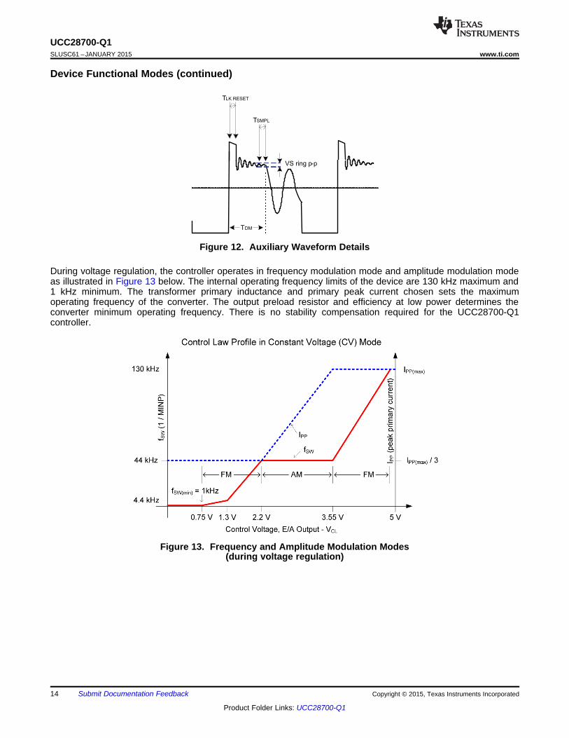
During voltage regulation, the controller operates in frequency modulation mode and amplitude modulation modeas illustrated in Figure 13 below. The internal operating frequency limits of the device are 130 kHz maximum and1 kHz minimum. The transformer primary inductance and primary peak current chosen sets the maximumoperating frequency of the converter. The output preload resistor and efficiency at low power determines theconverter minimum operating frequency. There is no stability compensation required for the UCC28700-Q1controller.
Figure 13. Frequency and Amplitude Modulation Modes(during voltage regulation)
14 Submit Documentation Feedback Copyright © 2015, Texas Instruments Incorporated
Product Folder Links: UCC28700-Q1

tON tDM
TSW
IPP IS x NS/NP
UCC28700-Q1www.ti.com SLUSC61 –JANUARY 2015
Device Functional Modes (continued)7.4.2 Primary-Side Current RegulationTiming information at the VS pin and current information at the CS pin allow accurate regulation of the secondaryaverage current. The control law dictates that as power is increased in CV regulation and approaching CCregulation the primary-peak current is at IPP(max). Referring to Figure 14 below, the primary-peak current, turnsratio, secondary demagnetization time (tDM), and switching period (TSW) determine the secondary average outputcurrent. Ignoring leakage inductance effects, the average output current is given by Equation 6. When theaverage output current reaches the regulation reference in the current control block, the controller operates infrequency modulation mode to control the output current at any output voltage at or below the voltage regulationtarget as long as the auxiliary winding can keep VDD above the UVLO turn-off threshold.
Figure 14. Transformer Currents
(6)
Figure 15. Typical Target Output V-I Characteristic
Copyright © 2015, Texas Instruments Incorporated Submit Documentation Feedback 15
Product Folder Links: UCC28700-Q1

VDRV
VDS
UCC28700-Q1SLUSC61 –JANUARY 2015 www.ti.com
Device Functional Modes (continued)7.4.3 Valley-SwitchingThe UCC28700-Q1 utilizes valley-switching to reduce switching losses in the MOSFET, to reduce induced-EMI,and to minimize the turn-on current spike at the sense resistor. The controller operates in valley-switching in allload conditions unless the VDS ringing has diminished.
Referring to Figure 16 below, the UCC28700-Q1 operates in a valley-skipping mode in most load conditions tomaintain an accurate voltage or current regulation point and still switch on the lowest available VDS voltage.
Figure 16. Valley-Skipping Mode
7.4.4 Start-Up OperationUpon application of input voltage to the converter, the start-up resistor connected to VDD from the bulk capacitorvoltage (VBLK) charges the VDD capacitor. During charging of the VDD capacitor the device bias supply current isless than 1.5 µA. When VDD reaches the 21-V UVLO turn-on threshold, the controller is enabled and theconverter starts switching. The initial three cycles are limited to IPP(min). This allows sensing any initial input oroutput faults with minimal power delivery. After the initial three cycles at minimum IPP(min), the controller respondsto the condition dictated by the control law. The converter remains in discontinuous mode during charging of theoutput capacitor(s), maintaining a constant output current until the output voltage is in regulation.
16 Submit Documentation Feedback Copyright © 2015, Texas Instruments Incorporated
Product Folder Links: UCC28700-Q1

D2
RCS
+
±
DRV
CS
CDD
VDD
GND
RS1
RS2
VS
Np Ns
Na
RSTR
VAUX
VAC
CBC RLC
UCC28700-Q1SOT23-6
COUTVOUTNs RPL
VREG
CB2
VBLK
CB1
RCBC
D1
UCC28700-Q1www.ti.com SLUSC61 –JANUARY 2015
8 Applications and Implementation
NOTEInformation in the following applications sections is not part of the TI componentspecification, and TI does not warrant its accuracy or completeness. TI’s customers areresponsible for determining suitability of components for their purposes. Customers shouldvalidate and test their design implementation to confirm system functionality.
8.1 Application InformationThe UCC28700-Q1 flyback power supply controllers provides constant voltage (CV) and constant current (CC)output regulation to help meet USB-compliant adaptors and charger requirements. These devices use theinformation obtained from auxiliary winding sensing (VS) to control the output voltage and do not requireoptocoupler/TL431 feedback circuitry. Not requiring optocoupler feedback reduces the component count andmakes the design more cost effective.
8.2 Typical Application
Figure 17. Typical Application Circuit
Copyright © 2015, Texas Instruments Incorporated Submit Documentation Feedback 17
Product Folder Links: UCC28700-Q1

UCC28700-Q1SLUSC61 –JANUARY 2015 www.ti.com
Typical Application (continued)8.2.1 Design Requirements
Table 1. Design ParametersPARAMETER SYMBOL NOTES AND CONDITIONS MIN NOM MAX UNIT
INPUT CHARACTERISTICSInput Voltage VIN 100 115/230 240 VLine Frequency fLINE 47 50/60 64 HzNo Load Input Power PSB_CONV VIN = Nom, IO = 0 A 30 mWBrownout Voltage VIN(RUN) IO = Nom 70 VOUTPUT CHARACTERISTICSOutput Voltage VO VIN = Nom, IO = Nom 4.75 5 5.25 VOutput Voltage Ripple VRIPPLE VIN = Nom, IO = Max 0.1 VOutput Current IO VIN = Min to Max 1 1.05 AOutput OVP VOVP IOUT = Min to Max 5.75 VTransient Response
(0.1 A to 0.6 A) or (0.6 A to 0.1A)Load Step (VO = 4.1 V to 6 V) VOΔ 4.1 5 6 VVOΔ = 0.9 V for COUT calculationin applications section
SYSTEMS CHARACTERISTICSSwitching Frequency 105 kHzFull Load Efficiency (115/230 V η IO = 1 A 74% 76%RMS Input)
18 Submit Documentation Feedback Copyright © 2015, Texas Instruments Incorporated
Product Folder Links: UCC28700-Q1

UCC28700-Q1www.ti.com SLUSC61 –JANUARY 2015
8.2.2 Detailed Design Procedure
This procedure outlines the steps to design a constant-voltage, constant-current flyback converter using theUCC28700-Q1 controller. Please refer to the Figure 17 for circuit details and section Device Nomenclature forvariable definitions used in the applications equations below.
8.2.2.1 Transformer Parameter VerificationThe transformer turns ratio selected affects the MOSFET VDS and secondary rectifier reverse voltage so theseshould be reviewed. The UCC28700-Q1 controller requires a minimum on time of the MOSFET (TON) andminimum DMAG time (TDMAG) of the secondary rectifier in the high line, minimum load condition. The selection ofFMAX, LP and RCS affects the minimum TON and TDMAG.
The secondary rectifier and MOSFET voltage stress can be determined by the equations below.
(7)
For the MOSFET VDS voltage stress, an estimated leakage inductance voltage spike (VLK) needs to be included.
(8)
The following equations are used to determine if the minimum TON target of 300 ns and minimum TDMAG target of1.1 µs is achieved.
(9)
(10)
8.2.2.2 Output CapacitanceThe output capacitance value is typically determined by the transient response requirement from no-load. Forexample, in some USB charger applications there is a requirement to maintain a minimum VO of 4.1 V with aload-step transient of 0 mA to 500 mA . The equation below assumes that the switching frequency can be at theUCC28700-Q1 minimum of fSW(min).
(11)
Another consideration of the output capacitor(s) is the ripple voltage requirement which is reviewed based onsecondary peak current and ESR. A margin of 20% is added to the capacitor ESR requirement in the equationbelow.
(12)
Copyright © 2015, Texas Instruments Incorporated Submit Documentation Feedback 19
Product Folder Links: UCC28700-Q1

RS1 = VIN:run ; × ¾2
NPA × IVSL (run )
UCC28700-Q1SLUSC61 –JANUARY 2015 www.ti.com
8.2.2.3 VDD Capacitance, CDD
The capacitance on VDD needs to supply the device operating current until the output of the converter reachesthe target minimum operating voltage in constant-current regulation. At this time the auxiliary winding can sustainthe voltage to the UCC28700-Q1. The total output current available to the load and to charge the outputcapacitors is the constant-current regulation target. The equation below assumes the output current of theflyback is available to charge the output capacitance until the minimum output voltage is achieved. There is anestimated 1 mA of gate-drive current in the equation and 1 V of margin added to VDD.
(13)
8.2.2.4 VDD Start-Up Resistance, RSTR
Once the VDD capacitance is known, the start-up resistance from VBULK to achieve the turn-on time target can bedetermined.
(14)
8.2.2.5 VS Resistor Divider, Line Compensation, and Cable CompensationThe VS divider resistors determine the output voltage regulation point of the flyback converter, also the high-sidedivider resistor (RS1) determines the line voltage at which the controller enables continuous DRV operation. RS1is initially determined based on transformer auxiliary to primary turns ratio and desired input voltage operatingthreshold.
(15)
The low-side VS pin resistor is selected based on desired VO regulation voltage.
(16)
The UCC28700-Q1 can maintain tight constant-current regulation over input line by utilizing the linecompensation feature. The line compensation resistor (RLC) value is determined by current flowing in RS1 andexpected gate drive and MOSFET turn-off delay. Assume a 50-ns internal delay in the UCC28700-Q1.
(17)
On the UCC28700-Q1 which has adjustable cable compensation, the resistance for the desired compensationlevel at the output terminals can be determined using the equation below.
(18)
20 Submit Documentation Feedback Copyright © 2015, Texas Instruments Incorporated
Product Folder Links: UCC28700-Q1

UCC28700-Q1www.ti.com SLUSC61 –JANUARY 2015
8.2.2.6 Input Bulk Capacitance and Minimum Bulk VoltageDetermine the minimum voltage on the input capacitance, CB1 and CB2 total, in order to determine the maximumNp to Ns turns ratio of the transformer. The input power of the converter based on target full-load efficiency,minimum input RMS voltage, and minimum AC input frequency are used to determine the input capacitancerequirement.
Maximum input power is determined based on VOCV, IOCC, and the full-load efficiency target.
(19)
The below equation provides an accurate solution for input capacitance based on a target minimum bulkcapacitor voltage. To target a given input capacitance value, iterate the minimum capacitor voltage to achieve thetarget capacitance.
(20)
Copyright © 2015, Texas Instruments Incorporated Submit Documentation Feedback 21
Product Folder Links: UCC28700-Q1

UCC28700-Q1SLUSC61 –JANUARY 2015 www.ti.com
8.2.2.7 Transformer Turns Ratio, Inductance, Primary-Peak CurrentThe maximum primary-to-secondary turns ratio can be determined by the target maximum switching frequency atfull load, the minimum input capacitor bulk voltage, and the estimated DCM quasi-resonant time.
Initially determine the maximum available total duty cycle of the on time and secondary conduction time based ontarget switching frequency and DCM resonant time. For DCM resonant time, assume 500 kHz if you do not havean estimate from previous designs. For the transition mode operation limit, the period required from the end ofsecondary current conduction to the first valley of the VDS voltage is ½ of the DCM resonant period, or 1 µsassuming 500-kHz resonant frequency. DMAX can be determined using the equation below.
(21)
Once DMAX is known, the maximum turns ratio of the primary to secondary can be determined with the equationbelow. DMAGCC is defined as the secondary diode conduction duty cycle during constant-current, CC, operation. Itis set internally by the UCC28700-Q1 at 0.425. The total voltage on the secondary winding needs to bedetermined; which is the sum of VOCV, the secondary rectifier VF, and the cable compensation voltage (VOCBC).For the 5-V USB charger applications, a turns ratio range of 13 to 15 is typically used.
(22)
Once an optimum turns ratio is determined from a detailed transformer design, use this ratio for the followingparameters.
The UCC28700-Q1 controller constant-current regulation is achieved by maintaining a maximum DMAG duty cycleof 0.425 at the maximum primary current setting. The transformer turns ratio and constant-current regulatingvoltage determine the current sense resistor for a target constant current.
Since not all of the energy stored in the transformer is transferred to the secondary, a transformer efficiency termis included. This efficiency number includes the core and winding losses, leakage inductance ratio, and biaspower ratio to rated output power. For a 5-V, 1-A charger example, bias power of 1.5% is a good estimate. Anoverall transformer efficiency of 0.9 is a good estimate to include 3.5% leakage inductance, 5% core and windingloss, and 1.5% bias power.
(23)
The primary transformer inductance can be calculated using the standard energy storage equation for flybacktransformers. Primary current, maximum switching frequency and output and transformer power losses areincluded in the equation below. Initially determine transformer primary current.
Primary current is simply the maximum current sense threshold divided by the current sense resistance.
(24)
(25)
The secondary winding to auxiliary winding transformer turns ratio (NAS) is determined by the lowest targetoperating output voltage in constant-current regulation and the VDD UVLO of the UCC28700-Q1. There isadditional energy supplied to VDD from the transformer leakage inductance energy which allows a lower turnsratio to be used in many designs.
(26)
22 Submit Documentation Feedback Copyright © 2015, Texas Instruments Incorporated
Product Folder Links: UCC28700-Q1

UCC28700-Q1www.ti.com SLUSC61 –JANUARY 2015
8.2.2.8 Standby Power EstimateAssuming no-load standby power is a critical design parameter, determine estimated no-load power based ontarget converter maximum switching frequency and output power rating.
The following equation estimates the stand-by power of the converter.
(27)
For a typical USB charger application, the bias power during no-load is approximately 2.5 mW. This is based on25-V VDD and 100-µA bias current. The output preload resistor can be estimated by VOCV and the difference inthe converter stand-by power and the bias power. The equation for output preload resistance accounts for biaspower estimated at 2.5 mW.
(28)
Typical start-up resistance values for RSTR range from 13 MΩ to 20 MΩ to achieve 1-s start-up time. Thecapacitor bulk voltage for the loss estimation is the highest voltage for the stand-by power measurement,typically 325 VDC.
(29)
For the total stand-by power estimation add an estimated 2.5 mW for snubber loss to the start-up resistance andconverter stand-by power loss.
(30)
Copyright © 2015, Texas Instruments Incorporated Submit Documentation Feedback 23
Product Folder Links: UCC28700-Q1
UCC28700-Q1SLUSC61 –JANUARY 2015 www.ti.com
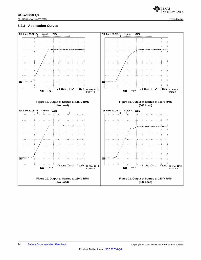
8.2.3 Application Curves
Figure 18. Output at Startup at 115-V RMS Figure 19. Output at Startup at 115-V RMS(No Load) (5-Ω Load)
Figure 20. Output at Startup at 230-V RMS Figure 21. Output at Startup at 230-V RMS(No Load) (5-Ω Load)
24 Submit Documentation Feedback Copyright © 2015, Texas Instruments Incorporated
Product Folder Links: UCC28700-Q1

UCC28700-Q1www.ti.com SLUSC61 –JANUARY 2015
CH1 = IO, CH4 = VO With a 5-V OffsetCH1 = IO, CH4 = VO With a 5-V Offset
Figure 23. Load Transients:Figure 22. Load Transients:(0.6-A to 0.1-A Load Step)(0.1-A to 0.6-A Load Step)
CH4 = VO, Output voltage at EVM outputCH2 = VO, Output voltage measured at the end of the 3M of cable in parallel with a 1-uF capacitor.The output voltage has less than 50 mV of output ripple at the end of the cable.
Figure 24. Output Ripple Voltage at Full Load
Copyright © 2015, Texas Instruments Incorporated Submit Documentation Feedback 25
Product Folder Links: UCC28700-Q1

UCC28700-Q1SLUSC61 –JANUARY 2015 www.ti.com
9 Power Supply RecommendationsThe UCC28700-Q1 is intended for AC/DC converters with input voltage range of 85 VAC(rms) to 265 VAC(rms) usingFlyback topology. It can be used in other applications and converter topologies with different input voltages. Besure that all voltages and currents are within the recommended operating conditions and absolute maximumratings of the device.
To maintain output current regulation over the entire input voltage range, design the converter to operate close tofMAX when in full-load conditions.
To improve thermal performance increase the copper area connected to GND pins.
10 Layout
10.1 Layout Guidelines• High frequency bypass Capacitor C7 should be placed arcos Pin 2 and 5 as close as you can get it to the
pins.• Resistor R15 and C7 form a low pass filter and the connection of R15 and C7 should be as close to the VDD
pin as possible.• C9 should be put as close to CS pin and R10 as possible. This forms a low pass filter with R10.• The connection for C9 and R10 should be as close to the CS pin as possible.• Please note that C9 may not be required in all designs. However, it is wise to put a place holder for it in your
design.• The VS pin controls the output voltage through the transformer turns ratio and the voltage divider of R7 and
R9. Note the trace with between the R7, R9 and VS pin should be; as short as; possible to reduce/eliminatepossible EMI coupling.
• Note the IC ground and power ground should meet at the bulk capacitor’s (C4 and C5) return. Tri to ensurethat high frequency/high current from the power stage does not go through the signal ground.– The high frequency/high current path that you need to be cautious of on the primary is C4, C5 +, T1
(P1,P2), Q1d, Q1s, R13 to the return of C4 and C5.• Try to keep all high current loops as short as possible.• Keep all high current/high frequency traces away from or perpendicular to other traces in the design.• Traces on the voltage clamp formed by D1, R1, D4 and C4 as short as possible.• C4 return needs to be as close to the bulk capacitor supply as possible. This reduces the magnitude of dv/dt
caused by large di/dt.• Avoid mounting semiconductors under magnetics.
26 Submit Documentation Feedback Copyright © 2015, Texas Instruments Incorporated
Product Folder Links: UCC28700-Q1

D2
Line
Nuetral
VOUT+
VOUT-
TP4
TP3
TP1
TP3
D5
T1J1J2
R3
R2 R10C8
C2
C3
C4
R11
R15
R5
R1
JMP2
JMP3
Q1
C9
C6
R7
R9
C7
R8
R4
D4
C1
D1
L1
R6
C5
D3
R13
R12
U1
UCC28700-Q1www.ti.com SLUSC61 –JANUARY 2015
Layout Guidelines (continued)
Figure 25. 5-W USB Adapter Schematic
10.2 Layout Example
Figure 26. Layout Example
Copyright © 2015, Texas Instruments Incorporated Submit Documentation Feedback 27
Product Folder Links: UCC28700-Q1
UCC28700-Q1SLUSC61 –JANUARY 2015 www.ti.com
11 Device and Documentation Support
11.1 Device Support
11.1.1 Device Nomenclature
11.1.1.1 Capacitance Terms in FaradsCBULK total input capacitance of CB1 and CB2.
CDD minimum required capacitance on the VDD pin.
COUT minimum output capacitance required.
11.1.1.2 Duty Cycle TermsDMAGCC secondary diode conduction duty cycle in CC, 0.425.
DMAX MOSFET on-time duty cycle.
11.1.1.3 Frequency Terms in HertzfLINE minimum line frequency.
fMAX target full-load maximum switching frequency of the converter.
fMIN minimum switching frequency of the converter, add 15% margin over the fSW(min) limit of the device.
fSW(min) minimum switching frequency (see the Electrical Characteristics table)
11.1.1.4 Current Terms in AmperesIOCC converter output constant-current target.
IPP(max) maximum transformer primary current.
ISTART start-up bias supply current (see the Electrical Characteristics table).
ITRAN required positive load-step current.
IVSL(run) VS pin run current (see the Electrical Characteristics table).
11.1.1.5 Current and Voltage Scaling TermsKAM maximum-to-minimum peak primary current ratio (see the Electrical Characteristics table).
KLC current-scaling constant (see the Electrical Characteristics table).
11.1.1.6 Transformer TermsLP transformer primary inductance.
NAS transformer auxiliary-to-secondary turns ratio.
NPA transformer primary-to-auxiliary turns ratio.
NPS transformer primary-to-secondary turns ratio.
11.1.1.7 Power Terms in WattsPIN converter maximum input power.
POUT full-load output power of the converter.
PRSTR VDD start-up resistor power dissipation.
PSB total stand-by power.
PSB_CONV PSB minus start-up resistor and snubber losses.
28 Submit Documentation Feedback Copyright © 2015, Texas Instruments Incorporated
Product Folder Links: UCC28700-Q1

UCC28700-Q1www.ti.com SLUSC61 –JANUARY 2015
Device Support (continued)11.1.1.8 Resistance Terms in ΩRCS primary current programming resistance
RESR total ESR of the output capacitor(s).
RPL preload resistance on the output of the converter.
RS1 high-side VS pin resistance.
RS2 low-side VS pin resistance.
RSTR maximum start-up resistance to achieve the turn-on time target.
RSTR VDD start-up resistance.
11.1.1.9 Timing Terms in SecondsTD current-sense delay including MOSFET turn-off delay; add 50 ns to MOSFET delay.
TDMAG(min) minimum secondary rectifier conduction time.
TON(min) minimum MOSFET on time.
TR resonant frequency during the DCM (discontinuous conduction mode) time.
TSTR converter start-up time requirement.
Copyright © 2015, Texas Instruments Incorporated Submit Documentation Feedback 29
Product Folder Links: UCC28700-Q1

UCC28700-Q1SLUSC61 –JANUARY 2015 www.ti.com
Device Support (continued)11.1.1.10 Voltage Terms in VoltsVBLK highest bulk capacitor voltage for stand-by power measurement.
VBULK(min) minimum voltage on CB1 and CB2 at full power.
VOCBC target cable compensation voltage at the output terminals.
VCBC(max) maximum voltage at the CBC pin at the maximum converter output current (see the ElectricalCharacteristics table).
VCCR constant-current regulating voltage (see the Electrical Characteristics table).
VCST(max) CS pin maximum current-sense threshold (see the Electrical Characteristics table).
VCST(min) CS pin minimum current-sense threshold (see the Electrical Characteristics table).
VDD(off) UVLO turn-off voltage (see the Electrical Characteristics table).
VDD(on) UVLO turn-on voltage (see the Electrical Characteristics table).
VOΔ output voltage drop allowed during the load-step transient.
VDSPK peak MOSFET drain-to-source voltage at high line.
VF secondary rectifier forward voltage drop at near-zero current.
VFA auxiliary rectifier forward voltage drop.
VLK estimated leakage inductance energy reset voltage.
VOCV regulated output voltage of the converter.
VOCC target lowest converter output voltage in constant-current regulation.
VREV peak reverse voltage on the secondary rectifier.
VRIPPLE output peak-to-peak ripple voltage at full-load.
VVSR CV regulating level at the VS input (see the Electrical Characteristics table).
11.1.1.11 AC Voltage Terms in VRMS
VIN(max) maximum input voltage to the converter.
VIN(min) minimum input voltage to the converter.
VIN(run) converter input start-up (run) voltage.
11.1.1.12 Efficiency TermsηSB estimated efficiency of the converter at no-load condition, not including start-up resistance or bias
losses. For a 5-V USB charger application, 60% to 65% is a good initial estimate.
η converter overall efficiency.
ηXFMR transformer primary-to-secondary power transfer efficiency.
30 Submit Documentation Feedback Copyright © 2015, Texas Instruments Incorporated
Product Folder Links: UCC28700-Q1

UCC28700-Q1www.ti.com SLUSC61 –JANUARY 2015
11.2 Documentation Support
11.2.1 Related DocumentationFor related documentation see the following:
Using the UCC28700EVM-068, Evaluation Module, SLUU968
11.3 TrademarksAll trademarks are the property of their respective owners.
11.4 Electrostatic Discharge CautionThese devices have limited built-in ESD protection. The leads should be shorted together or the device placed in conductive foamduring storage or handling to prevent electrostatic damage to the MOS gates.
12 Mechanical, Packaging, and Orderable InformationThe following pages include mechanical, packaging, and orderable information. This information is the mostcurrent data available for the designated devices. This data is subject to change without notice and revision ofthis document. For browser-based versions of this data sheet, refer to the left-hand navigation.
Copyright © 2015, Texas Instruments Incorporated Submit Documentation Feedback 31
Product Folder Links: UCC28700-Q1

PACKAGE OPTION ADDENDUM
www.ti.com 29-Jan-2015
Addendum-Page 1
PACKAGING INFORMATION
Orderable Device Status(1)
Package Type PackageDrawing
Pins PackageQty
Eco Plan(2)
Lead/Ball Finish(6)
MSL Peak Temp(3)
Op Temp (°C) Device Marking(4/5)
Samples
UCC28700QDBVRQ1 ACTIVE SOT-23 DBV 6 3000 Green (RoHS& no Sb/Br)
CU NIPDAU Level-1-260C-UNLIM -40 to 125 700Q
(1) The marketing status values are defined as follows:ACTIVE: Product device recommended for new designs.LIFEBUY: TI has announced that the device will be discontinued, and a lifetime-buy period is in effect.NRND: Not recommended for new designs. Device is in production to support existing customers, but TI does not recommend using this part in a new design.PREVIEW: Device has been announced but is not in production. Samples may or may not be available.OBSOLETE: TI has discontinued the production of the device.
(2) Eco Plan - The planned eco-friendly classification: Pb-Free (RoHS), Pb-Free (RoHS Exempt), or Green (RoHS & no Sb/Br) - please check http://www.ti.com/productcontent for the latest availabilityinformation and additional product content details.TBD: The Pb-Free/Green conversion plan has not been defined.Pb-Free (RoHS): TI's terms "Lead-Free" or "Pb-Free" mean semiconductor products that are compatible with the current RoHS requirements for all 6 substances, including the requirement thatlead not exceed 0.1% by weight in homogeneous materials. Where designed to be soldered at high temperatures, TI Pb-Free products are suitable for use in specified lead-free processes.Pb-Free (RoHS Exempt): This component has a RoHS exemption for either 1) lead-based flip-chip solder bumps used between the die and package, or 2) lead-based die adhesive used betweenthe die and leadframe. The component is otherwise considered Pb-Free (RoHS compatible) as defined above.Green (RoHS & no Sb/Br): TI defines "Green" to mean Pb-Free (RoHS compatible), and free of Bromine (Br) and Antimony (Sb) based flame retardants (Br or Sb do not exceed 0.1% by weightin homogeneous material)
(3) MSL, Peak Temp. - The Moisture Sensitivity Level rating according to the JEDEC industry standard classifications, and peak solder temperature.
(4) There may be additional marking, which relates to the logo, the lot trace code information, or the environmental category on the device.
(5) Multiple Device Markings will be inside parentheses. Only one Device Marking contained in parentheses and separated by a "~" will appear on a device. If a line is indented then it is a continuationof the previous line and the two combined represent the entire Device Marking for that device.
(6) Lead/Ball Finish - Orderable Devices may have multiple material finish options. Finish options are separated by a vertical ruled line. Lead/Ball Finish values may wrap to two lines if the finishvalue exceeds the maximum column width.
Important Information and Disclaimer:The information provided on this page represents TI's knowledge and belief as of the date that it is provided. TI bases its knowledge and belief on informationprovided by third parties, and makes no representation or warranty as to the accuracy of such information. Efforts are underway to better integrate information from third parties. TI has taken andcontinues to take reasonable steps to provide representative and accurate information but may not have conducted destructive testing or chemical analysis on incoming materials and chemicals.TI and TI suppliers consider certain information to be proprietary, and thus CAS numbers and other limited information may not be available for release.
In no event shall TI's liability arising out of such information exceed the total purchase price of the TI part(s) at issue in this document sold by TI to Customer on an annual basis.

PACKAGE OPTION ADDENDUM
www.ti.com 29-Jan-2015
Addendum-Page 2
OTHER QUALIFIED VERSIONS OF UCC28700-Q1 :
• Catalog: UCC28700
NOTE: Qualified Version Definitions:
• Catalog - TI's standard catalog product

TAPE AND REEL INFORMATION
*All dimensions are nominal
Device PackageType
PackageDrawing
Pins SPQ ReelDiameter
(mm)
ReelWidth
W1 (mm)
A0(mm)
B0(mm)
K0(mm)
P1(mm)
W(mm)
Pin1Quadrant
UCC28700QDBVRQ1 SOT-23 DBV 6 3000 178.0 9.0 3.23 3.17 1.37 4.0 8.0 Q3
PACKAGE MATERIALS INFORMATION
www.ti.com 19-Jun-2015
Pack Materials-Page 1

*All dimensions are nominal
Device Package Type Package Drawing Pins SPQ Length (mm) Width (mm) Height (mm)
UCC28700QDBVRQ1 SOT-23 DBV 6 3000 180.0 180.0 18.0
PACKAGE MATERIALS INFORMATION
www.ti.com 19-Jun-2015
Pack Materials-Page 2


IMPORTANT NOTICE
Texas Instruments Incorporated and its subsidiaries (TI) reserve the right to make corrections, enhancements, improvements and otherchanges to its semiconductor products and services per JESD46, latest issue, and to discontinue any product or service per JESD48, latestissue. Buyers should obtain the latest relevant information before placing orders and should verify that such information is current andcomplete. All semiconductor products (also referred to herein as “components”) are sold subject to TI’s terms and conditions of salesupplied at the time of order acknowledgment.TI warrants performance of its components to the specifications applicable at the time of sale, in accordance with the warranty in TI’s termsand conditions of sale of semiconductor products. Testing and other quality control techniques are used to the extent TI deems necessaryto support this warranty. Except where mandated by applicable law, testing of all parameters of each component is not necessarilyperformed.TI assumes no liability for applications assistance or the design of Buyers’ products. Buyers are responsible for their products andapplications using TI components. To minimize the risks associated with Buyers’ products and applications, Buyers should provideadequate design and operating safeguards.TI does not warrant or represent that any license, either express or implied, is granted under any patent right, copyright, mask work right, orother intellectual property right relating to any combination, machine, or process in which TI components or services are used. Informationpublished by TI regarding third-party products or services does not constitute a license to use such products or services or a warranty orendorsement thereof. Use of such information may require a license from a third party under the patents or other intellectual property of thethird party, or a license from TI under the patents or other intellectual property of TI.Reproduction of significant portions of TI information in TI data books or data sheets is permissible only if reproduction is without alterationand is accompanied by all associated warranties, conditions, limitations, and notices. TI is not responsible or liable for such altereddocumentation. Information of third parties may be subject to additional restrictions.Resale of TI components or services with statements different from or beyond the parameters stated by TI for that component or servicevoids all express and any implied warranties for the associated TI component or service and is an unfair and deceptive business practice.TI is not responsible or liable for any such statements.Buyer acknowledges and agrees that it is solely responsible for compliance with all legal, regulatory and safety-related requirementsconcerning its products, and any use of TI components in its applications, notwithstanding any applications-related information or supportthat may be provided by TI. Buyer represents and agrees that it has all the necessary expertise to create and implement safeguards whichanticipate dangerous consequences of failures, monitor failures and their consequences, lessen the likelihood of failures that might causeharm and take appropriate remedial actions. Buyer will fully indemnify TI and its representatives against any damages arising out of the useof any TI components in safety-critical applications.In some cases, TI components may be promoted specifically to facilitate safety-related applications. With such components, TI’s goal is tohelp enable customers to design and create their own end-product solutions that meet applicable functional safety standards andrequirements. Nonetheless, such components are subject to these terms.No TI components are authorized for use in FDA Class III (or similar life-critical medical equipment) unless authorized officers of the partieshave executed a special agreement specifically governing such use.Only those TI components which TI has specifically designated as military grade or “enhanced plastic” are designed and intended for use inmilitary/aerospace applications or environments. Buyer acknowledges and agrees that any military or aerospace use of TI componentswhich have not been so designated is solely at the Buyer's risk, and that Buyer is solely responsible for compliance with all legal andregulatory requirements in connection with such use.TI has specifically designated certain components as meeting ISO/TS16949 requirements, mainly for automotive use. In any case of use ofnon-designated products, TI will not be responsible for any failure to meet ISO/TS16949.
Products ApplicationsAudio www.ti.com/audio Automotive and Transportation www.ti.com/automotiveAmplifiers amplifier.ti.com Communications and Telecom www.ti.com/communicationsData Converters dataconverter.ti.com Computers and Peripherals www.ti.com/computersDLP® Products www.dlp.com Consumer Electronics www.ti.com/consumer-appsDSP dsp.ti.com Energy and Lighting www.ti.com/energyClocks and Timers www.ti.com/clocks Industrial www.ti.com/industrialInterface interface.ti.com Medical www.ti.com/medicalLogic logic.ti.com Security www.ti.com/securityPower Mgmt power.ti.com Space, Avionics and Defense www.ti.com/space-avionics-defenseMicrocontrollers microcontroller.ti.com Video and Imaging www.ti.com/videoRFID www.ti-rfid.comOMAP Applications Processors www.ti.com/omap TI E2E Community e2e.ti.comWireless Connectivity www.ti.com/wirelessconnectivity
Mailing Address: Texas Instruments, Post Office Box 655303, Dallas, Texas 75265Copyright © 2016, Texas Instruments Incorporated