ucc28600 120-w evaluation module user's guide (rev. a) · www .ti.com 3 schematic schematic a...
TRANSCRIPT

UCC28600 120-W Evaluation Module
User's Guide
October 2006 Power Supply MAN
SLUU256A
UCC28600 120-W Evaluation Module
User's Guide
Literature Number: SLUU256A
August 2006–Revised October 2006
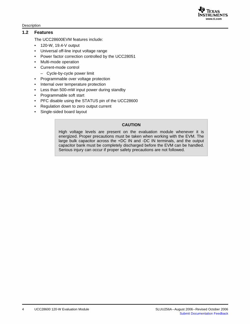
1 Description
1.1 Applications
User's GuideSLUU256A–August 2006–Revised October 2006
UCC28600 120-W Evaluation Module
The UCC28600 evaluation module (EVM) is a 120-W off-line quasi-resonant flybackconverter providing a 19.4-V regulated output at 6.2 A of load current, operating from auniversal ac input. The front-end power factor correction (PFC) stage is controlled bythe UCC28051 and accommodates an input line voltage range of 85 VRMS to 265VRMS and is designed to meet EIC61000-3-2 harmonic emissions requirements. Themodule uses the UCC28600 Quasi-Resonant Flyback Green-Mode Controller whichintegrates built-in state of the art energy saving features with high level protectionfeatures to provide cost effective solutions for energy efficient power supplies.
The UCC28600EVM highlights the many benefits of using the UCC28600 Quasi-Resonant FlybackGreen-Mode Controller. Low system parts count and multifunction pins in this green-mode controllerprovide a cost-effective solution while meeting stringent world-wide energy efficiency requirements. Lowvoltage switching reduces switching losses and improves efficiency. Green-mode and frequency-foldbackmode operation reduces the operating frequency at light loads and no-load operation. A dedicatedSTATUS pin is used to disable the PFC controller when the converter has entered standby.
This user’s guide provides the schematic, component list, assembly drawing for a single-sided PCBapplication, artwork, and test set up necessary to evaluate the UCC28600 in a typical off-line converterapplication.
The UCC28600 is suited for use in isolated off-line systems requiring high-efficiency and advanced faultprotection features including:
• Bias supplies for LCD monitors, LCD TV, PDP TV, and set top boxes• AC/DC adapters• Offline battery chargers• Energy efficient power supplies up to 200 W
SLUU256A–August 2006–Revised October 2006 UCC28600 120-W Evaluation Module 3Submit Documentation Feedback
www.ti.com
1.2 Features
Description
The UCC28600EVM features include:
• 120-W, 19.4-V output• Universal off-line input voltage range• Power factor correction controlled by the UCC28051• Multi-mode operation• Current-mode control
– Cycle-by-cycle power limit• Programmable over voltage protection• Internal over temperature protection• Less than 500-mW input power during standby• Programmable soft start• PFC disable using the STATUS pin of the UCC28600• Regulation down to zero output current• Single-sided board layout
CAUTION
High voltage levels are present on the evaluation module whenever it isenergized. Proper precautions must be taken when working with the EVM. Thelarge bulk capacitor across the +DC IN and -DC IN terminals, and the outputcapacitor bank must be completely discharged before the EVM can be handled.Serious injury can occur if proper safety precautions are not followed.
UCC28600 120-W Evaluation Module4 SLUU256A–August 2006–Revised October 2006Submit Documentation Feedback
www.ti.com
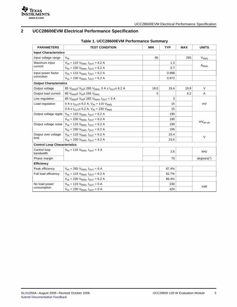
2 UCC28600EVM Electrical Performance Specification
UCC28600EVM Electrical Performance Specification
Table 1. UCC28600EVM Performance Summary
PARAMETERS TEST CONDITION MIN TYP MAX UNITS
Input Characteristics
Input voltage range VIN 85 265 VRMS
Maximum input VIN = 115 VRMS, IOUT = 6.2 A 1.3ARMScurrent VIN = 230 VRMS, IOUT = 6.2 A 0.7
Input power factor VIN = 115 VRMS, IOUT = 6.2 A 0.998correction VIN = 230 VRMS, IOUT = 6.2 A 0.972
Output Characteristics
Output voltage 85 VRMS≤ VIN≤ 265 VRMS, 0 A ≤ IOUT≤ 6.2 A 19.0 19.4 19.8 V
Output load current 85 VRMS≤ VIN≤ 265 VRMS 0 6.2 A
Line regulation 85 VRMS≤ VIN≤ 265 VRMS, IOUT = 3 A 3
Load regulation 0 A ≤ IOUT≤ 6.2 A, VIN = 115 VRMS 15 mV
0 A ≤ IOUT≤ 6.2 A, VIN = 230 VRMS 15
Output voltage ripple VIN = 115 VRMS, IOUT = 6.2 A 190
VIN = 230 VRMS, IOUT = 6.2 A 190mVpk=pk
Output voltage noise VIN = 115 VRMS, IOUT = 6.2 A 190
VIN = 230 VRMS, IOUT = 6.2 A 190
Output over voltage VIN = 115 VRMS, IOUT = 6.2 A 23.4Vlimit VIN = 230 VRMS, IOUT = 6.2 A 23.6
Control Loop Characteristics
Control loop VIN = 115 VRMS, IOUT = 3 A 2.6 kHzbandwidth
Phase margin 70 degrees(°)
Efficiency
Peak efficiency VIN = 265 VRMS, IOUT = 6 A 87.4%
Full load efficiency VIN = 115 VRMS, IOUT = 6.2 A 82.7%
VIN = 230 VRMS, IOUT = 6.2 A 86.4%
No load power VIN = 115 VRMS, IOUT = 0 A 230mWconsumption VIN = 230 VRMS, IOUT = 0 A 420
SLUU256A–August 2006–Revised October 2006 UCC28600 120-W Evaluation Module 5Submit Documentation Feedback

www.ti.com
3 Schematic
Schematic
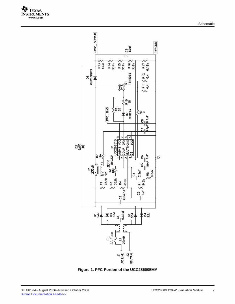
A schematic of the UCC28600EVM is shown in Figures 1 and 2. Terminal block J1 is the ac input voltagesource connector, J2 is the 19.4-V output, and J3 is the output voltage return. The +DC IN and –DC INconnectors are used to monitor the PFC output voltage or can be used to supply a dc input voltage whenthe PFC stage is disabled.
Figure 1 shows the PFC controller, the UCC28051, with all the discrete circuitry for configuring the powerfactor correction at the universal line input range. The bias to the UCC28051 controller is provided by theauxiliary winding of the quasi-resonant flyback inductor and controlled by the STATUS output of theUCC28600 controller. During light load operation, the bias to the PFC controller is removed, enabling theconverter to operate at high efficiencies.
Figure 2 shows the green-mode controller, the UCC28600, with all the discrete circuitry for configuring theisolated quasi-resonant flyback converter using the PFC output voltage as its input. The auxiliary windingprovides the bias to the controllers and provides over voltage protection and valley switching information,as well as bias to the UCC28600 and UCC28051. The series resistor connected between the currentsense pin and the current sense resistor programs the power limit of the converter. The seriescombination of R41 and D18 adds an offset voltage to the current sense signal that effectively reducesaudible noise during standby operation by limiting the current in the transformer during operation in theaudible frequency range.
6 UCC28600 120-W Evaluation Module SLUU256A–August 2006–Revised October 2006Submit Documentation Feedback
www.ti.com
4A F
use
F1
+
Schematic
Figure 1. PFC Portion of the UCC28600EVM
SLUU256A–August 2006–Revised October 2006 UCC28600 120-W Evaluation Module 7Submit Documentation Feedback

www.ti.com
+
+
++
+
Schematic
Figure 2. Quasi-Resonant Flyback Portion of the UCC28600EVM
8 UCC28600 120-W Evaluation Module SLUU256A–August 2006–Revised October 2006Submit Documentation Feedback
www.ti.com
4 EVM Test Setup
AC SOURCEPOWER METERDMM 1 VOUTDMM 2 IOUT
Electronic Load
+ + ++ + + −−−
−−−
−
+
DMM3VBULK
+ −
Ripple Scope
A H I A EXTA LOVHI VLO
FAN
EVM Test Setup
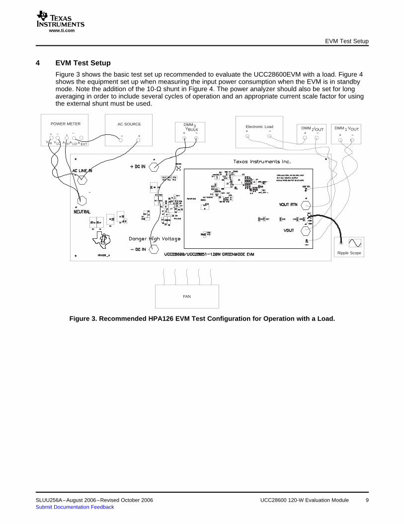
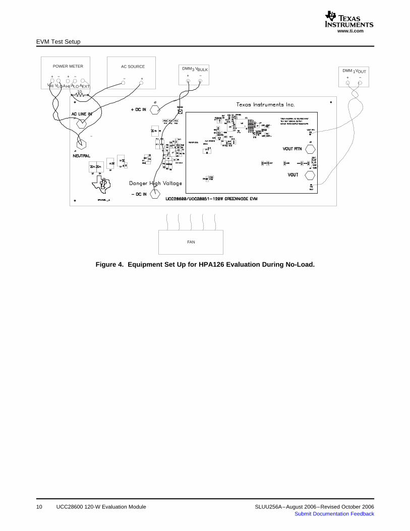
Figure 3 shows the basic test set up recommended to evaluate the UCC28600EVM with a load. Figure 4shows the equipment set up when measuring the input power consumption when the EVM is in standbymode. Note the addition of the 10-Ω shunt in Figure 4. The power analyzer should also be set for longaveraging in order to include several cycles of operation and an appropriate current scale factor for usingthe external shunt must be used.
Figure 3. Recommended HPA126 EVM Test Configuration for Operation with a Load.
SLUU256A–August 2006–Revised October 2006 UCC28600 120-W Evaluation Module 9Submit Documentation Feedback
www.ti.com
AC SOURCEPOWER METERDMM 1 VOUT
+ + + + −−−−
−
+
DMM3 VBULK
+ −
AHI AEXTALOVHI VLO
FAN
10
EVM Test Setup
Figure 4. Equipment Set Up for HPA126 Evaluation During No-Load.
10 UCC28600 120-W Evaluation Module SLUU256A–August 2006–Revised October 2006Submit Documentation Feedback
www.ti.com
4.1 Power Meter
4.2 AC Input Source
4.3 Digital Multimeters
4.4 Output Load
4.5 Recommended Wire Gauge
4.6 Fan
EVM Test Setup
The power analyzer shall be capable of measuring low input current, typically less than 10 mA, and a longaveraging mode if low power standby mode input power measurements are to be taken. An example ofsuch an analyzer is the Voltech PM100 Single Phase Power Analyzer. To measure the intermittent burstsof current and power drawn from the line during no-load operation, an external 10-Ω shunt, with a currentscale factor of 10 V/A, was used at a high sample rate over an extended period of time in order to displaythe averaged results (refer to Figure 4).
The input source shall be a variable ac source capable of supplying between 85 VRMS and 265 VRMS at noless than 5-A peak and connected to the AC LINE IN terminal on the EVM, as shown in Figure 2. Foraccurate efficiency calculations, a power meter should be inserted between the neutral line of the acsource and the NEUTRAL terminal of the EVM. For highest accuracy, connect the voltage terminals of thepower meter directly across the AC LINE IN and NEUTRAL terminals.
Digital multimeters are used to measure the bulk dc voltage into the quasi-resonant converter stage(DMM3), the output load current (DMM2), and the regulated output voltage (DMM1).
For the output load, a programmable electronic load set to constant current mode and capable of sinking 0to 7 ADC at 20 VDC shall be used. For highest accuracy, VOUT can be monitored by connecting a dcvoltmeter, DMM1, directly across the VOUT and VOUT RTN test points as shown in Figure 2. A dc currentmeter, DMM2, should be placed in series with the electronic load for accurate output currentmeasurements.
The connection between the source voltage and the EVM input terminals can carry as much as 2 A peak.The minimum recommended wire size is AWG #20 with the total length of wire less than 8 feet (4 feetinput, 4 feet return). The connection between the EVM output terminals and the load can carry as much as6.2 A. The minimum recommended wire size is AWG #16, with the total length of wire less than 8 feet (4feet output, 4 feet return).
Because this evaluation module is not enclosed, allowing probing of circuit nodes, a small fan capable of200 LFM to 400 LFM should be used to reduce component temperatures when operating at or above 50%maximum rated load current.
SLUU256A–August 2006–Revised October 2006 UCC28600 120-W Evaluation Module 11Submit Documentation Feedback
www.ti.com
5 Power-Up/Power-Down Procedure
Power-Up/Power-Down Procedure
The following test procedure is recommended primarily for power up and shutting down the evaluationmodule. The fan should be turned on whenever the EVM is running. Also, never leave a powered EVMunattended for any length of time.
1. Working at an ESD workstation, make sure that an ionizer is on before the EVM is removed from theprotective packaging and power is applied to the EVM. Electrostatic smock and safety glasses shouldalso be worn. Because voltages in excess of 400 V may be present on the EVM, do not connect theground strap from the smock to the bench.
2. Power Up
a. Prior to connecting the ac input source, it is advisable to limit the source current to 5 A maximum.Make sure the ac source is initially set between 85 VRMS and 265 VRMS prior to turning on. Connectthe ac source to the AC LINE IN and NEUTRAL terminals of the EVM as shown in Figure 3.
b. Connect the voltage terminals of the power analyzer across AC LINE IN and NEUTRAL as shownin Figures 3 and 4.
c. Connect the current meter terminals of the power analyzer in series with the NEUTRAL line asshown in Figure 3.
a. If no-load input power measurements are to be made, set the power analyzer to long averagingand external shunt mode. Insert a shunt, such as a 10-Ω resistor as shown in Figure 4, in serieswith the NEUTRAL terminal of the EVM. Set the appropriate current scale on the poweranalyzer.
d. Connect DMM1 across VOUT and VOUT RTN as shown in Figures 3 and 4.e. For operation with a load, connect the positive terminal of the LOAD to the VOUT terminal of the
EVM and the negative terminal of the LOAD to the VOUT RTN terminal of the EVM, as shown inFigure 3. Connect DMM2 in series with the negative terminal as shown in Figure 3. Set the LOAD toconstant current mode to sink 0 A.
f. Connect DMM3 across +DC IN and – DC IN as shown in Figures 3 and 4.g. Make sure the output capacitor bank is completely discharged prior to power up.h. Turn on the ac source and observe that the output is regulating to 19.4 V.i. Increase load from 0 A up to 6.2 A.
3. Power Down
a. Turn off ac source.b. Discharge the output capacitor bank.c. Turn off the load.
UCC28600 120-W Evaluation Module12 SLUU256A–August 2006–Revised October 2006Submit Documentation Feedback
www.ti.com
6 UCC28600EVM Performance Data and Characteristic Curves
5 V/div.
t − Time − 5.0 ms/div .
VOUT(os) = 1.1 V at IOUT = 6.2 A
5 V/div.
t − Time − 5.0 ms/div .
VOUT(os) = 1.1 V at IOUT = 6.2 A
t − Time − 2.0 ms/div .
200 mV/div .200 mV/div .
t − Time − 2.0 ms/div .
UCC28600EVM Performance Data and Characteristic Curves
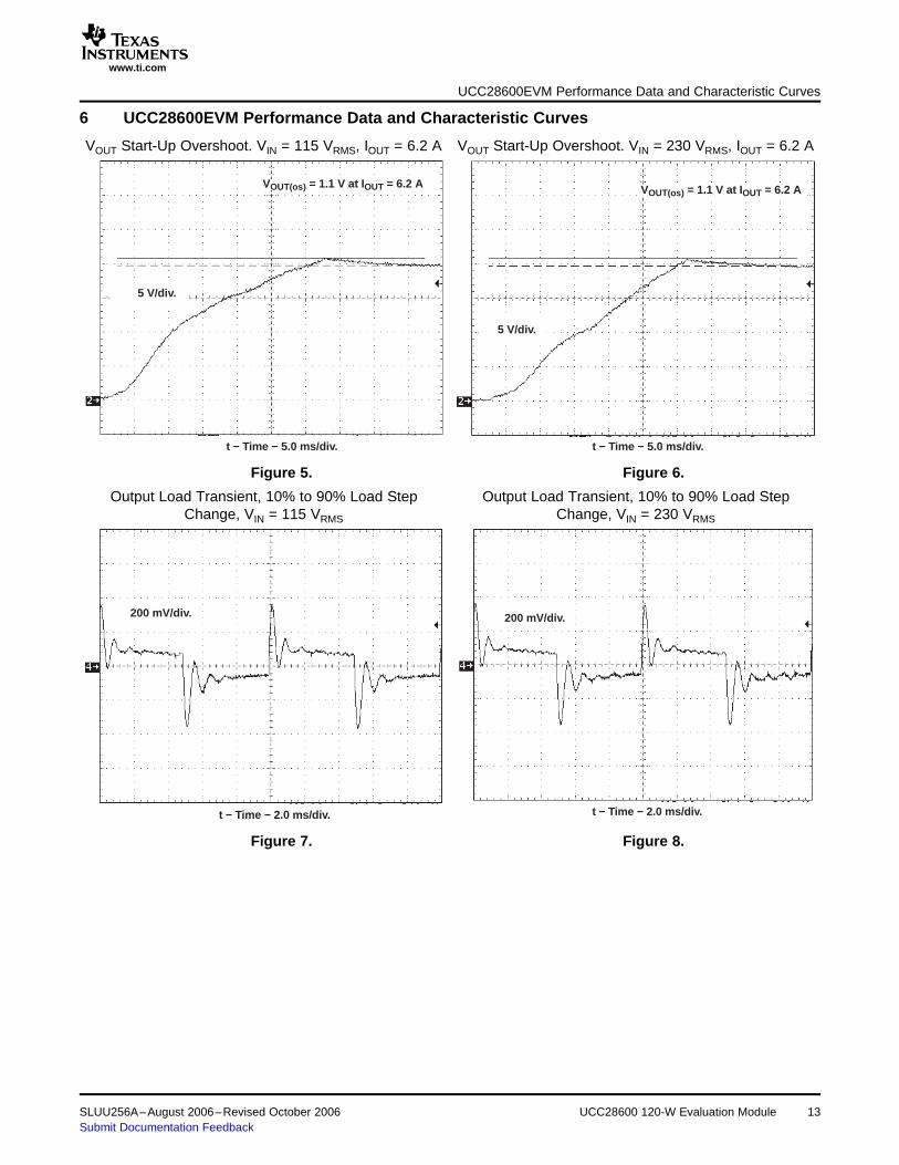
VOUT Start-Up Overshoot. VIN = 115 VRMS, IOUT = 6.2 A VOUT Start-Up Overshoot. VIN = 230 VRMS, IOUT = 6.2 A
Figure 5. Figure 6.
Output Load Transient, 10% to 90% Load Step Output Load Transient, 10% to 90% Load StepChange, VIN = 115 VRMS Change, VIN = 230 VRMS
Figure 7. Figure 8.
SLUU256A–August 2006–Revised October 2006 UCC28600 120-W Evaluation Module 13Submit Documentation Feedback

www.ti.com
20 mV/div .
t − Time − 200 s/div.
20 mV/div .
t − Time − 200 s/div.
50 mV/div .
t − Time − 5.0 µs/div.
20 mV/div .
t − Time − 5.0 ms/div .
UCC28600EVM Performance Data and Characteristic Curves
Output Voltage Ripple and Noise, Green Mode, VIN = Output Voltage Ripple and Noise, VIN = 115 VRMS, IOUT230 VRMS, IOUT = 0.5 A = 0.5 A
Figure 9. Figure 10.
Output Voltage Ripple and Noise, VIN = 230 VRMS, IOUT= 6.2 A No Load Output Voltage Ripple, VIN = 230 VRMS
Figure 11. Figure 12.
14 UCC28600 120-W Evaluation Module SLUU256A–August 2006–Revised October 2006Submit Documentation Feedback

www.ti.com
20 mV/div .
t − Time − 5.0 ms/div .
DrainCH1: 200 V/div .
GateCH2: 10 V/div .
FBCH3: 1.0 V/div .CSCH4: 500 mV/div .
t − Time − 25 µs/div.
DrainCH1: 200 V/div .
GateCH2:10 V/div .
FBCH3: 5.0 V/div .
CSCH4:1.0 V/div .
t − Time − 2.5 µs/div.
DrainCH1: 200 V/div .
GateCH2: 10 V/div .
FBCH3: 1.0 V/div .
CSCH4: 500 mV/div .
t − Time − 200 µs/div.
UCC28600EVM Performance Data and Characteristic Curves
Green Mode, Burst Pulses at 40 kHz, VIN = 115 VRMS,No Load Output Voltage Ripple, VIN = 115 VRMS IOUT = 0.2 A
Figure 13. Figure 14.
Green Mode Showing Frequency of Burst Packets Frequency Foldback Mode, Switching Frequency =Equal to 900 Hz , VIN = 115 VRMS, IOUT = 0.2 A 115 kHz, VIN = 115 VRMS, IOUT = 1.6 A
Figure 15. Figure 16.
SLUU256A–August 2006–Revised October 2006 UCC28600 120-W Evaluation Module 15Submit Documentation Feedback

www.ti.com
DrainCH1: 200 V/div .
GateCH2: 10 V/div .
FB
CH3: 5.0 mV/div .
CSCH4: 1.0 V/div .
t − Time − 2.5 µs/div.
DrainCH1:200V/div.
GateCH2: 10V/div .
FBCH3: 5 V/div .CS
CH4: 1.0 V/div .
t − Time − 2.5 µs/div.
−20
0
10
30
−15
−5
5
20
25
1E + 02 1E + 041E + 03
−10
15
Gain
Phase
−80
0
40
120
−60
−20
20
80
100
−40
60
PHASE/GAINvs.
FREQUENCY
f − Frequency − Hz
Gai
n −
dB
Pha
se −
O
0.0
10
15
25
20
0.0 122 104 6 8
5
OUTPUT VOLTAGEvs.
OUTPUT CURRENT
IOUT − Output Current − A
VO
UT
− O
utpu
t Vol
tage
− V
UCC28600EVM Performance Data and Characteristic Curves
Discontinuous Current Mode, Switching Frequency = Quasi-Resonant Mode, Switching Frequency = 116130 kHz, VIN = 115 VRMS, IOUT = 4.6 A kHz, VIN = 115 VRMS, IOUT = 5.6 A
Figure 17. Figure 18.
Figure 19. Figure 20.
16 UCC28600 120-W Evaluation Module SLUU256A–August 2006–Revised October 2006Submit Documentation Feedback
www.ti.com
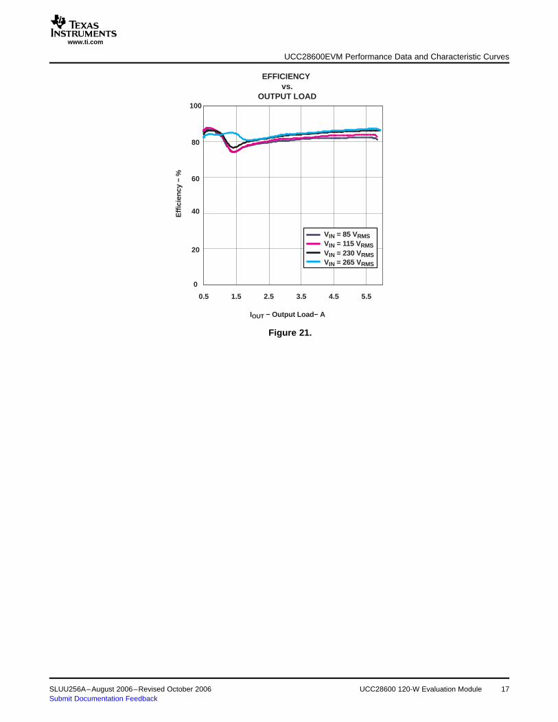
EFFICIENCY vs.
OUTPUT LOAD
IOUT − Output Load− A
Effi
cien
cy −
%
0
100
20
0.5 2.5 3.51.5 4.5 5.5
40
60
80
VIN = 85 VRMSVIN = 115 VRMSVIN = 230 VRMSVIN = 265 VRMS
UCC28600EVM Performance Data and Characteristic Curves
Figure 21.
SLUU256A–August 2006–Revised October 2006 UCC28600 120-W Evaluation Module 17Submit Documentation Feedback
www.ti.com
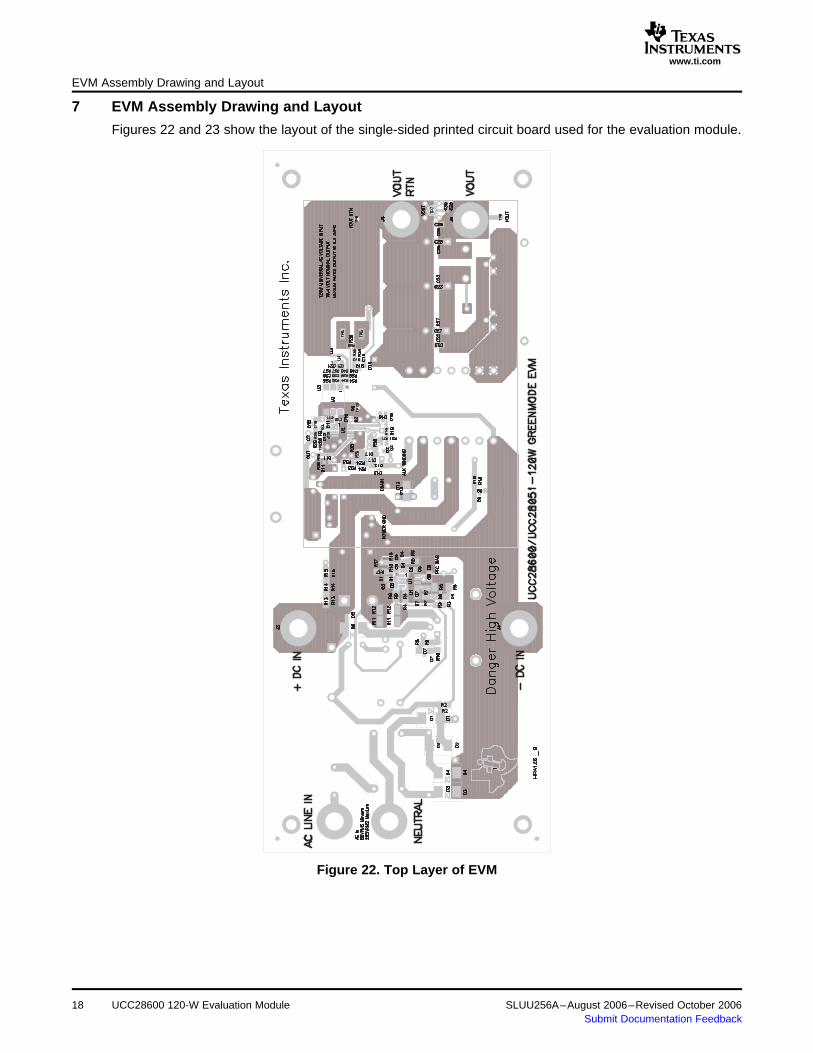
7 EVM Assembly Drawing and Layout
EVM Assembly Drawing and Layout
Figures 22 and 23 show the layout of the single-sided printed circuit board used for the evaluation module.
Figure 22. Top Layer of EVM
18 UCC28600 120-W Evaluation Module SLUU256A–August 2006–Revised October 2006Submit Documentation Feedback

www.ti.com
R31
R32
EVM Assembly Drawing and Layout
Figure 23. Bottom Layer of EVM
SLUU256A–August 2006–Revised October 2006 UCC28600 120-W Evaluation Module 19Submit Documentation Feedback

www.ti.com
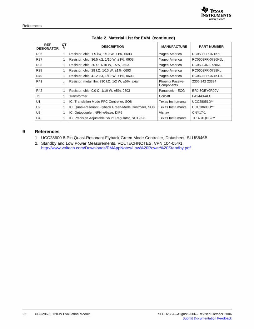
8 List of MaterialsList of Materials
Table 2. Material List for EVM (1) (2)
REF QT DESCRIPTION MANUFACTURE PART NUMBERDESIGNATOR Y
C1 Capacitor, metal poly, 0.39 µF, 630 V, -40/+85 °C, ±10%, ST Microelectronics ECQ-E6394KF1 0.236 x 1.043
C2 Capacitor, metal poly, 0.047 µF, 630 V, -40/+85 °C, ±10%, ST Microelectronics ECQ-E6473KF1 0.709 x 0.236
C3, C6 2 Capacitor, ceramic, 1 nF, 50 V, X7R, ±10%, 0805 ON Semiconductor C0805C102K5RACTU
C4 1 Capacitor, ceramic, 2.2 µF, 16 V, X7R, ±10%, 1206 Diodes Inc ECJ-3YB1C225K
C5 1 Capacitor, ceramic, 10 nF, 50 V, X7R, ±10%, 0805 Littelfuse C0805C103K5RACTU
C7 Capacitor, ceramic, 47 pF, 50 V, C0G, ±5%, 0805 Cooper Electronic C0805C470J5GACTU1 Technologies
C8 Capacitor, ceramic, 0.1 µF, 25 V, X7R, ±10%, 0805 Cooper Electronic ECJ-2VB1E104K1 Technologies
C9 Capacitor, aluminum electrolytic, 82 µF, 450 VDC, -40/+85 Coilcraft EET-ED2W820CA1 °C, ±20%, 0.984 inch Dia.
C10 Capacitor, ceramic, 0.022 µF, 25 V, X7R, ±10%, 0603 Infineon ECJ-1VB1E223K1 Technologies
C11 Capacitor, ceramic, 390 pF, 50 V, X7R, ±10%, 0603 Infineon GRM188R71H391KA01D1 Technologies
C12 Capacitor, ceramic, 100 pF, 100 V, C0G, ±5%, 0603 infineon GRM1885C2A101JA01D1 Technologies
C13 Capacitor, electrolytic, 10 µF, 100 V, -40/+105 °C, ±20%, Yageo America EEU-FC2A1001 0.200 inch
C14 Capacitor, ceramic, 1 µF, 50 V, X7R, ±10%, 0.200 x 0.256 Yageo America B37984M5105K0001 inch
C15 Capacitor, ceramic, 0.1 µF, 50 V, X7R, ±10%, 0.200 x Yageo America B37987F5104K0541 0.256 inch
C16 Capacitor, ceramic disc, 1 nF, 1 kV, X5R, ±10%, 0.265 x Panasonic - ECG 562R-10TSD101 0.472 inch
C17 Capacitor, polyester Film, 0.01 µF, 630 V, -40/+85 °C, Panasonic - ECG ECQ-E6103KF1 ±10%, 0.472 x 0.177 inch
C18 1 Capacitor, ceramic, 0.1 µF, 16 V, X7R, ±10%, 0603 Kemet C0603C104M4RACTU
C19 Capacitor, ceramic disc, 4.7 nF, 250 V, -25/+85 °C, ±20%, Panasonic - ECG ECK-ANA472ME1 0.394 x 0.315 inch
C20 1 Capacitor, ceramic, 220pF, 100 V, C0G, ±5%, 0603 Murata Electronics GRM1885C2A221JA01D
C21 Capacitor, ceramic, 0.22 µF, 25 V, X7R, ±10%, 0603 AVX 06033D224KAT2A1 CORPORATION
C22, C23, Capacitor, ceramic, 1 µF, 25 V, X5R, ±10%, 0805 Panasonic - ECG ECJ-2FB1E105KC25, C27, 6C29, C30
C24, C26, C28 Capacitor, aluminum electrolytic, 1800 µF, 25 V, ±20%, United Chemi-Con EKZE250ELL182MK30S3 0.571 inch
C31 1 Capacitor, electrolytic, 33 µF, 50 V, ±20%, 0.200 inch Panasonic - ECG EEU-FC1H330
D1, D2, D3, D4 4 Diode, rectifer GPP, 3 A, 600 V, SMC Diodes Inc S3J-13-F
D5 1 Diode, rectifier, 6 A, 400 A peak surge, 600 V, P600 Diodes Inc 6A6-T
D6, D7 2 Diode, fast recovery, 2 A, 600 V, SMA ST Microelectronics STTH2R06A
D8 1 Diode, ultra fast, 3 A, 600 V, SMC ON Semiconductor MURS360T3
D9 1 Diode, zener, 500 mW, 18 V, SOD-123 ON Semiconductor MMSZ18T1
D11 Diode, schottky, 1 A, 40 V, SOT-23 Central ZHCS10001 Semiconductor
D12, D17 2 Diode, ultra fast rectifier, 1 A, 100 V, SMA ON Semiconductor MURA110T3
(1) These assemblies are ESD sensitive, ESD precautions shall be observed.(2) These assemblies must comply with workmanship standards IPC-A-610 Class 2.
20 UCC28600 120-W Evaluation Module SLUU256A–August 2006–Revised October 2006Submit Documentation Feedback

www.ti.com
List of Materials
Table 2. Material List for EVM (continued)
REF QT DESCRIPTION MANUFACTURE PART NUMBERDESIGNATOR Y
D13 1 Diode, fast rectifier, 2 A, 600 V, SMB STMicroelectronics STTH2R06U
D14, D15 2 Diode, dual schottky, 2x10 A, 100 V, TO-220AB STMicroelectronics STPS20H100CT
D16 1 Diode, zener, 500 mW, 10 V, SOD-123 ON Semiconductor MMSZ5240BT1
D18 1 Diode, signal, 300 mA, 75 V, 350 mW, SOD-123 Diodes Inc 1N4148W-7
F1 1 Fuse, axial, fast acting, 4 A, 250 V, 0.145 x 0.300 inch Littelfuse 0263004.M
L1 Inductor, dual winding, 27 mH, 1.032 x 1.043 inch Cooper Electronic CTX16-169261 Technologies
L2 Xfmr, boost inductor, 232 µH, 1.122 x 1.122 inch Cooper Electronic CTX16-172981 Technologies
L3 1 Inductor, power choke, 4.7 µH, 0.500 inch Coilcraft PCV-0-472-10L
Q1 MOSFET, N-channel, 650 V, 11 A, 380 mΩ, TO-220V Infineon 11N60S51 Technologies
Q2 Bipolar, PNP, 40V, 200mA, SOT-23 Infineon MMBT3906LT11 Technologies
Q3 MOSFET, cool MOS power N-channel, 800 V, 11 A, 450 Infineon SPP11N80C31 mΩ, TO-220AB Technologies
R1 1 Resistor, chip, 10.2 kΩ, 1/4 W, ±1%, 1206 Yageo America RC1206FR-0710K2L
R2, R3, R4, Resistor, chip, 332 kΩ, 1/4 W, ±1%, 1206 Yageo America 9C12063A3323FKHFT6R14, R15, R16
R5 1 Resistor, chip, 6.04 kΩ, 1/4 W, ±1%, 1206 Yageo America 9C12063A6041FKHFT
R6 1 Resistor, chip, 100 Ω, 1/2 W, ±1%, 2010 Panasonic - ECG ERJ-12SF1000U
R7 1 Resistor, chip, 10 kΩ, 1/4 W, ±1%, 1210 Panasonic - ECG ERJ-14NF1002U
R8 1 Resistor, chip, 20 Ω, 1/4 W, ±1%, 1206 Yageo America RC1206FR-0720RL
R9 1 Resistor, chip, 0 Ω, 1/4 W, ±5%, 1206 Yageo America 9C12063A0R00JLHFT
R10 1 Resistor, chip, 10 Ω, 1/4 W, ±1%, 1206 Yageo America 9C12063A10R0FKHFT
R11, R12 2 Resistor, chip, 0.4 Ω, 1 W, ±1%, 2512 Vishay/Dale WSL2512R4000FEA
R13 1 Resistor, chip, 49.9 Ω, 1/4 W, ±1%, 1206 Yageo America RC1206FR-0749R9L
R17 1 Resistor, chip, 6.19 kΩ, 1/4 W, ±1%, 1206 Yageo America RC1206FR-076K19L
R18 1 Resistor, chip, 200 Ω, 1/8 W, ±1%, 0805 Rohm MCR10EZHF2000
R19 1 Resistor, chip, 5.6 kΩ, 1/10 W, ±5%, 0603 Rohm MCR03EZPJ562
R20 1 Resistor, chip, 47 Ω, 1/8 W, ±1%, 0805 Rohm MCR10EZHF47R0
R21 1 Resistor, chip, 8.2 kΩ, 1/10 W, ±5%, 0603 Yageo America RC0603JR-078K2L
R22 1 Resistor, metal film, 680 kΩ, 1/4 W, ±1%, axial, RN55 Panasonic - ECG ERO-S2PHF6803
R23, R24 2 Resistor, chip, 680 kΩ, 1/4 W, ±5%, 1206 Rohm ERJ-8GEYJ684V
R25 1 Resistor, chip, 20 Ω, 1/10 W, ±5%, 0603 Panasonic - ECG ERJ-3GEYJ200V
R26 1 Resistor, chip, 10 Ω, 1/16 W, ±1%, 0603 Panasonic - ECG ERJ-3EKF10R0V
R27 1 Resistor, metal film, 200 kΩ, 1/4 W, ±1%, axial, RN55 Yageo America MFR-25FRF-200K
R28 Resistor, metal film, 35.7 kΩ, 1/4 W, ±1%, 0.300 X 0.100 Yageo America MFR-25FBF-35K71 inch
R29 1 Resistor, chip, 1.78 kΩ, 1/10 W, ±1%, 0603 Rohm MCR03EZPFX2051
R30 1 Resistor, metal film, 10 kΩ, 1/4 W, ±1%, axial, RN55 Panasonic - ECG ERO-S2PHF1002
R31 Resistor, metal oxide, 47 Ω, 3 W, ±5%, 1.300 X 0.205 inch RCD Components RMF3-470-J1 Inc.
R32 Resistor, metal oxide, 15 kΩ, 3 W, ±5%, 1.300 X 0.205 Panasonic - ECG P15KW-3BK-ND1 inch
R33 Resistor, wirewound, 0.13 Ω, 3 W, ±1%, axial, 0.600 X Huntington Electric ALSR-3-.13-1%1 0.250 inch
R34, R35 2 Resistor, chip, 499 Ω, 1/10 W, ±1%, 0603 Yageo America RC0603FR-07499RL
SLUU256A–August 2006–Revised October 2006 UCC28600 120-W Evaluation Module 21Submit Documentation Feedback
www.ti.com
9 References
References
Table 2. Material List for EVM (continued)
REF QT DESCRIPTION MANUFACTURE PART NUMBERDESIGNATOR Y
R36 1 Resistor, chip, 1.5 kΩ, 1/10 W, ±1%, 0603 Yageo America RC0603FR-071K5L
R37 1 Resistor, chip, 36.5 kΩ, 1/10 W, ±1%, 0603 Yageo America RC0603FR-0736K5L
R38 1 Resistor, chip, 20 Ω, 1/10 W, ±5%, 0603 Yageo America RC0603JR-0720RL
R39 1 Resistor, chip, 28 kΩ, 1/10 W, ±1%, 0603 Yageo America RC0603FR-0728KL
R40 1 Resistor, chip, 4.12 kΩ, 1/10 W, ±1%, 0603 Yageo America RC0603FR-074K12L
R41 Resistor, metal film, 330 kΩ, 1/2 W, ±5%, axial Phoenix Passive 2306 242 233341 Components
R42 1 Resistor, chip, 0.0 Ω, 1/10 W, ±5%, 0603 Panasonic - ECG ERJ-3GEY0R00V
T1 1 Transformer Coilcaft FA2443-ALC
U1 1 IC, Transistion Mode PFC Controller, SO8 Texas Instrumants UCC28051D**
U2 1 IC, Quasi-Resonant Flyback Green-Mode Controller, SO8 Texas Instrumants UCC28600D**
U3 1 IC, Optocoupler, NPN w/base, DIP6 Vishay CNY17-1
U4 1 IC, Precision Adjustable Shunt Regulator, SOT23-3 Texas Instrumants TL1431QDBZ**
1. UCC28600 8-Pin Quasi-Resonant Flyback Green Mode Controller, Datasheet, SLUS646B2. Standby and Low Power Measurements, VOLTECHNOTES, VPN 104-054/1,
http://www.voltech.com/Downloads/PMAppNotes/Low%20Power%20Standby.pdf
22 UCC28600 120-W Evaluation Module SLUU256A–August 2006–Revised October 2006Submit Documentation Feedback
IMPORTANT NOTICE
Texas Instruments Incorporated and its subsidiaries (TI) reserve the right to make corrections, modifications,enhancements, improvements, and other changes to its products and services at any time and to discontinueany product or service without notice. Customers should obtain the latest relevant information before placingorders and should verify that such information is current and complete. All products are sold subject to TI’s termsand conditions of sale supplied at the time of order acknowledgment.
TI warrants performance of its hardware products to the specifications applicable at the time of sale inaccordance with TI’s standard warranty. Testing and other quality control techniques are used to the extent TIdeems necessary to support this warranty. Except where mandated by government requirements, testing of allparameters of each product is not necessarily performed.
TI assumes no liability for applications assistance or customer product design. Customers are responsible fortheir products and applications using TI components. To minimize the risks associated with customer productsand applications, customers should provide adequate design and operating safeguards.
TI does not warrant or represent that any license, either express or implied, is granted under any TI patent right,copyright, mask work right, or other TI intellectual property right relating to any combination, machine, or processin which TI products or services are used. Information published by TI regarding third-party products or servicesdoes not constitute a license from TI to use such products or services or a warranty or endorsement thereof.Use of such information may require a license from a third party under the patents or other intellectual propertyof the third party, or a license from TI under the patents or other intellectual property of TI.
Reproduction of information in TI data books or data sheets is permissible only if reproduction is withoutalteration and is accompanied by all associated warranties, conditions, limitations, and notices. Reproductionof this information with alteration is an unfair and deceptive business practice. TI is not responsible or liable forsuch altered documentation.
Resale of TI products or services with statements different from or beyond the parameters stated by TI for thatproduct or service voids all express and any implied warranties for the associated TI product or service andis an unfair and deceptive business practice. TI is not responsible or liable for any such statements.
Following are URLs where you can obtain information on other Texas Instruments products and applicationsolutions:
Products Applications
Amplifiers amplifier.ti.com Audio www.ti.com/audio
Data Converters dataconverter.ti.com Automotive www.ti.com/automotive
DSP dsp.ti.com Broadband www.ti.com/broadband
Interface interface.ti.com Digital Control www.ti.com/digitalcontrol
Logic logic.ti.com Military www.ti.com/military
Power Mgmt power.ti.com Optical Networking www.ti.com/opticalnetwork
Microcontrollers microcontroller.ti.com Security www.ti.com/security
Low Power Wireless www.ti.com/lpw Telephony www.ti.com/telephony
Video & Imaging www.ti.com/video
Wireless www.ti.com/wireless
Mailing Address: Texas Instruments
Post Office Box 655303 Dallas, Texas 75265
Copyright 2006, Texas Instruments Incorporated