ucc2817, ucc2818, ucc3817 and ucc3818 bicmos ... necessary for active power factor-corrected...
TRANSCRIPT

Copyright © 2016, Texas Instruments Incorporated
VREF9
2
16
1
15
10
5
4
DRVOUT
GND
CAI
VCC
OVP/EN
VAOUT
1.9 V
PKLMT
7.5 V REFERENCE
UVLO
16 V/10 V (UCC2817)
10.5 V/10 V (UCC2818)
VCC
3
OSCILLATOR
12
RT
14
CT
S Q
R
PWM
LATCH
+
t PWM
CAOUT
+
t
+
t
+
t
SS
VOLTAGE
ERROR AMP
8.0 V
13
7
11VSENSE
VFF 8
IAC 6
MOUT
MIRROR
2:1
X2
+
t
7.5 V
ENABLE
OVP
yX
XMULT
OSC
CLK
CLK
CURRENT
AMP
16 V (FOR UCC2817 ONLY)
+
t0.33 VZERO POWER
R
+
t
Product
Folder
Sample &Buy
Technical
Documents
Tools &
Software
Support &Community
An IMPORTANT NOTICE at the end of this data sheet addresses availability, warranty, changes, use in safety-critical applications,intellectual property matters and other important disclaimers. PRODUCTION DATA.
UCC2817, UCC2818, UCC3817, UCC3818SLUS395K –FEBRUARY 2000–REVISED OCTOBER 2015
UCC2817, UCC2818, UCC3817 and UCC3818 BiCMOS Power Factor Pregulator
1
1 Features1• Controls Boost Preregulator to Near-Unity Power
Factor• Limits Line Distortion• World Wide Line Operation• Over-Voltage Protection• Accurate Power Limiting• Average Current Mode Control• Improved Noise Immunity• Improved Feed-Forward Line Regulation• Leading Edge Modulation• 150-μA Typical Start-Up Current• Low-Power BiCMOS Operation• Up to 18-V Operation• Frequency Range 6 kHz to 220 kHz
2 Applications• PC Power• Consumer Electronics• Lighting• Industrial Power Supplies• IEC6100-3-2 Compliant Supplies Less Than
300 W
3 DescriptionThe UCCx817 and UCCx818 family provides all thefunctions necessary for active power factor-correctedpreregulators. The controller achieves near-unitypower factor by shaping the AC input line currentwaveform to correspond to that of the AC input linevoltage. Average current mode control maintainsstable, low distortion sinusoidal line current.
Designed in Texas Instrument’s BiCMOS process,the UCCx817 and UCCx818 offers new features suchas lower start-up current, lower power dissipation,overvoltage protection, a shunt UVLO detect circuitry,a leading-edge modulation technique to reduce ripplecurrent in the bulk capacitor, and an improved, low-offset (±2-mV) current amplifier to reduce distortion atlight load conditions.
Device Information(1)
PART NUMBER PACKAGE BODY SIZE (NOM)UCC2817,UCC2818,UCC3817,UCC3818
SOIC (16)3.91 mm × 9.9 mm7.5 mm × 10.3 mm
PDIP (16) 6.35 mm × 19.3 mm
(1) For all available packages, see the orderable addendum atthe end of the data sheet.
Block Diagram

2
UCC2817, UCC2818, UCC3817, UCC3818SLUS395K –FEBRUARY 2000–REVISED OCTOBER 2015 www.ti.com
Product Folder Links: UCC2817 UCC2818 UCC3817 UCC3818
Submit Documentation Feedback Copyright © 2000–2015, Texas Instruments Incorporated
Table of Contents1 Features .................................................................. 12 Applications ........................................................... 13 Description ............................................................. 14 Revision History..................................................... 25 Pin Configuration and Functions ......................... 36 Specifications......................................................... 4
6.1 Absolute Maximum Ratings ...................................... 46.2 ESD Ratings.............................................................. 56.3 Recommended Operating Conditions....................... 56.4 Thermal Information .................................................. 56.5 Electrical Characteristics........................................... 56.6 Typical Characteristics .............................................. 8
7 Detailed Description .............................................. 97.1 Overview ................................................................... 97.2 Functional Block Diagram ......................................... 97.3 Feature Description................................................. 107.4 Device Functional Modes........................................ 13
8 Application and Implementation ........................ 158.1 Application Information............................................ 158.2 Typical Application ................................................. 16
9 Power Supply Recommendations ...................... 249.1 Power Switch Selection .......................................... 24
10 Layout................................................................... 2510.1 Layout Guidelines ................................................. 2510.2 Layout Example .................................................... 27
11 Device and Documentation Support ................. 2811.1 Documentation Support ....................................... 2811.2 Related Links ........................................................ 2811.3 Receiving Notification of Documentation Updates 2811.4 Community Resources.......................................... 2811.5 Trademarks ........................................................... 2811.6 Electrostatic Discharge Caution............................ 2811.7 Glossary ................................................................ 28
12 Mechanical, Packaging, and OrderableInformation ........................................................... 29
4 Revision History
Changes from Revision J (March 2009) to Revision K Page
• Added ESD Ratings table, Feature Description section, Device Functional Modes, Application and Implementationsection, Power Supply Recommendations section, Layout section, Device and Documentation Support section, andMechanical, Packaging, and Orderable Information section. ................................................................................................ 1

IMOUT
IIAC
(VVAOUT
1)
VVFF
2K
=×
×
–
1
2
3
4
5
6
7
8
16
15
14
13
12
11
10
9
GND
PKLMT
CAOUT
CAI
MOUT
IAC
VAOUT
VFF
DRVOUT
VCC
CT
SS
RT
VSENSE
OVP/EN
VREF
3
UCC2817, UCC2818, UCC3817, UCC3818www.ti.com SLUS395K –FEBRUARY 2000–REVISED OCTOBER 2015
Product Folder Links: UCC2817 UCC2818 UCC3817 UCC3818
Submit Documentation FeedbackCopyright © 2000–2015, Texas Instruments Incorporated
5 Pin Configuration and Functions
D, DW, N, and PW Packages16 Pins
Top View
Pin FunctionsPIN
I/O DESCRIPTIONNAME NO.
GND 1 – Ground. All voltages measured with respect to ground. VCC and REF should be bypasseddirectly to GND with a 0.1-μF or larger ceramic capacitor.
PKLMT 2 I
PFC peak current limit. The threshold for peak limit is 0 V. Use a resistor divider from thenegative side of the current sense resistor to VREF to level shift this signal to a voltage leveldefined by the value of the sense resistor and the peak current limit. Peak current limit isreached when PKLMT voltage falls below 0 V.
CAOUT 3 OCurrent amplifier output. This is the output of a wide bandwidth operational amplifier thatsenses line current and commands the PFC pulse-width modulator (PWM) to force thecorrect duty cycle. Compensation components are placed between CAOUT and MOUT.
CAI 4 ICurrent amplifier noninverting input. Place a resistor between this pin and the GND side ofcurrent sense resistor. This input and the inverting input (MOUT) remain functional down toand below GND.
MOUT 5 I/O
Multiplier output and current amplifier inverting input. The output of the analog multiplier andthe inverting input of the current amplifier are connected together at MOUT. As the multiplieroutput is a current, this is a high-impedance input so the amplifier can be configured as adifferential amplifier. This configuration improves noise immunity and allows for the leading-edge modulation operation. The multiplier output current is limited to (2 × IIAC). The multiplieroutput current is given by the equation:
where• K = 1/V is the multiplier gain constant (1)
IAC 6 ICurrent proportional to input voltage. This input to the analog multiplier is a currentproportional to instantaneous line voltage. The multiplier is tailored for very low distortionfrom this current input (IIAC) to multiplier output. The recommended maximum IIAC is 500 μA.
VAOUT 7 OVoltage amplifier output. This is the output of the operational amplifier that regulates outputvoltage. The voltage amplifier output is internally limited to approximately 5.5 V to preventovershoot.
VFF 8 I Feed-forward voltage. The RMS voltage signal generated at this pin by mirroring 1/2 of theIIAC into a single pole external filter. At low line, the VFF voltage should be 1.4 V.
VREF 9 O
Voltage reference output. VREF is the output of an accurate 7.5-V voltage reference. Thisoutput is capable of delivering 20 mA to peripheral circuitry, and is internally short-circuitcurrent-limited. VREF is disabled and remains at 0 V when VVCC is below the UVLOthreshold. Bypass VREF to GND with a 0.1-μF or larger ceramic capacitor for best stability.Refer to Figure 1 and Figure 2 for VREF line and load regulation characteristics.
OVP/EN 10 IOver-voltage/enable. A window comparator input that disables the output driver if the boostoutput voltage is a programmed level above the nominal ,or disables both the PFC outputdriver and resets SS if pulled below 1.9 V (typ).

4
UCC2817, UCC2818, UCC3817, UCC3818SLUS395K –FEBRUARY 2000–REVISED OCTOBER 2015 www.ti.com
Product Folder Links: UCC2817 UCC2818 UCC3817 UCC3818
Submit Documentation Feedback Copyright © 2000–2015, Texas Instruments Incorporated
Pin Functions (continued)PIN
I/O DESCRIPTIONNAME NO.
VSENSE 11 I Voltage amplifier inverting input. This is normally connected to a compensation network andto the boost converter output through a divider network.
RT 12 IOscillator charging current. A resistor from RT to GND is used to program oscillator chargingcurrent. A resistor between 10 kΩ and 100 kΩ is recommended. Nominal voltage on this pinis 3 V.
SS 13 I
Soft-start. VSS is discharged for VVCC low conditions. When enabled, SS charges an externalcapacitor with a current source. This voltage is used as the voltage error signal during start-up, enabling the PWM duty cycle to increase slowly. In the event of a VVCC dropout, theOVP/EN is forced below 1.9 V (typ), SS quickly discharges to disable the PWM. Note: In anopen-loop test circuit, grounding the SS pin does not ensure 0% duty cycle. See theApplication and Implementation for details.
CT 14 I
Oscillator timing capacitor. A capacitor from CT to GND sets the PWM oscillator frequencyaccording to:
f ≈ 0.6/(RT × CT) (2)The lead from the oscillator timing capacitor to GND should be as short and direct aspossible.
VCC 15 I
Positive supply voltage. Connect to a stable source of at least 20 mA between 10 V and 17V for normal operation. Bypass VCC directly to GND to absorb supply current spikesrequired to charge external MOSFET gate capacitances. To prevent inadequate gate drivesignals, the output devices are inhibited unless VVCC exceeds the upper undervoltagelockout voltage threshold and remains above the lower threshold.
DRVOUT 16 O
Gate drive. The output drive for the boost switch is a totem-pole MOSFET gate driver onDRVOUT. Use a series gate resistor to prevent interaction between the gate impedance andthe output driver that might cause the DRVOUT to overshoot excessively. See Figure 6 todetermine minimum required gate resister value. Some overshoot of the DRVOUT output isalways expected when driving a capacitive load.
(1) Stresses beyond those listed under Absolute Maximum Ratings may cause permanent damage to the device. These are stress ratingsonly, which do not imply functional operation of the device at these or any other conditions beyond those indicated under RecommendedOperating Conditions. Exposure to absolute-maximum-rated conditions for extended periods may affect device reliability.
6 Specifications
6.1 Absolute Maximum Ratingsover operating free-air temperature range (unless otherwise noted) (1)
MIN MAX UNITSupply voltage VCC 18 VSupply current ICC 20 mAGate drive current, continuous 0.2 AGate drive current 1.2 AInput voltage, CAI, MOUT, SS 8 VInput voltage, PKLMT 5 VInput voltage, VSENSE, OVP/EN 10 VInput current, RT, IAC, PKLMT 10 mAInput current, VCC (no switching) 20 mAMaximum negative voltage, DRVOUT, PKLMT, MOUT –0.5 VPower dissipation 1 W
TJ Junction temperature –55 150 °CTstg Storage temperature –65 150 °CTsol Lead temperature (soldering, 10 seconds) 300 °C

5
UCC2817, UCC2818, UCC3817, UCC3818www.ti.com SLUS395K –FEBRUARY 2000–REVISED OCTOBER 2015
Product Folder Links: UCC2817 UCC2818 UCC3817 UCC3818
Submit Documentation FeedbackCopyright © 2000–2015, Texas Instruments Incorporated
(1) JEDEC document JEP155 states that 500-V HBM allows safe manufacturing with a standard ESD control process.(2) JEDEC document JEP157 states that 250-V CDM allows safe manufacturing with a standard ESD control process.
6.2 ESD RatingsVALUE UNIT
V(ESD) Electrostatic dischargeHuman-body model (HBM), per ANSI/ESDA/JEDEC JS-001 (1) ±2000
VCharged-device model (CDM), per JEDEC specification JESD22-C101 (2) ±1500
6.3 Recommended Operating Conditionsover operating free-air temperature range (unless otherwise noted)
MIN NOM MAX UNITVCC Input voltage 12 VVSENSE Input sense voltage 7.5 10 V
Input current for oscillator 1.36 10 mA
(1) For more information about traditional and new thermal metrics, For more information about traditional and new thermal metrics, see theSemiconductor and IC Package Thermal Metrics application report.
(2) Specified θja (junction to ambient) is for devices mounted to 5-inch2 FR4 PC board with one ounce copper, where noted. Whenresistance range is given, lower values are for 5 inch2 aluminum PC board. Test PWB was 0.062-inch thick and typically used 0.635-mmtrace widths for power packages and 1.3-mm trace widths for non-power packages with a 100-mil × 100-mil probe land area at the endof each trace.
(3) Modeled data. If value range given for θja, lower value is for 3×3 inch. 1 oz internal copper ground plane, higher value is for 1×1-inch.ground plane. All model data assumes only one trace for each non-fused lead.
6.4 Thermal Information
THERMAL METRIC (1)
UCC281x, UCC381x
UNITSOIC (D) SOIC (DW) PDIP (N) TSSOP(PW)
16 PINS 16 PINS 16 PINS 16 PINSRθJA Junction-to-ambient thermal resistance 73.9 (2) 74.1 (2) 49.3 (2) 98.9 (3) °C/WRθJC(top) Junction-to-case (top) thermal resistance 33.5 35.5 38.9 30.2 (3) °C/WRθJB Junction-to-board thermal resistance 31.4 38.9 29.4 44.8 °C/WψJT Junction-to-top characterization parameter 5.8 9.9 18.9 1.9 °C/WψJB Junction-to-board characterization parameter 31.1 38.3 29.2 44.1 °C/W
6.5 Electrical CharacteristicsTA = 0°C to 70°C for the UCC3817, and TA = −40°C to 85°C for the UCC2817, TA = TJ, VCC = 12 V, RT = 22 kΩ, CT = 270pF, (unless otherwise noted)
PARAMETER TEST CONDITIONS MIN TYP MAX UNITSUPPLY CURRENT
Supply current, off VCC = (VCC turn-on threshold−0.3 V) 150 300 µA
Supply current, on VCC = 12 V, No load onDRVOUT 2 4 6 mA
UVLOVCC turn-on threshold (UCCx817) 15.4 16 16.6 VVCC turn-off threshold (UCCx817) 9.4 9.7 VUVLO hysteresis (UCCx817) 5.8 6.3 VMaximum shunt voltage (UCCx817) IVCC = 10 mA 15.4 17 17.5 VVCC turn-on threshold (UCCx818) 9.7 10.2 10.8 VVCC turn-off threshold (UCCx818) 9.4 9.7 VUVLO hysteresis (UCCx818) 0.3 0.5 V
VOLTAGE AMPLIFIER

6
UCC2817, UCC2818, UCC3817, UCC3818SLUS395K –FEBRUARY 2000–REVISED OCTOBER 2015 www.ti.com
Product Folder Links: UCC2817 UCC2818 UCC3817 UCC3818
Submit Documentation Feedback Copyright © 2000–2015, Texas Instruments Incorporated
Electrical Characteristics (continued)TA = 0°C to 70°C for the UCC3817, and TA = −40°C to 85°C for the UCC2817, TA = TJ, VCC = 12 V, RT = 22 kΩ, CT = 270pF, (unless otherwise noted)
PARAMETER TEST CONDITIONS MIN TYP MAX UNIT
(1) Ensured by design, not production tested.(2) Reference variation for VCC < V is shown in Figure 1.
Input voltageTA = 0°C to 70°C 7.387 7.5 7.613
VTA = −40°C to 85°C 7.369 7.5 7.631
VSENSE bias current VSENSE = VREF, VAOUT = 2.5V 50 200 nA
Open loop gain VAOUT = 2 V to 5 V 50 90 dBHigh-level output voltage IL = −150 μA 5.3 5.5 5.6 VLow-level output voltage IL = 150 μA 0 50 150 mV
OVERVOLTAGE PROTECTION AND ENABLEOver voltage reference VREF +0.48 VREF +0.50 VREF +0.52 VHysteresis 300 500 600 mVEnable threshold 1.7 1.9 2.1 VEnable hysteresis 0.1 0.2 0.3 V
CURRENT AMPLIFIERInput offset voltage VCM = 0 V, VCAOUT = 3 V –3.5 0 2.5 mVInput bias current VCM = 0 V, VCAOUT = 3 V –50 –100 nAInput offset current VCM = 0 V, VCAOUT = 3 V 25 100 nA
Open loop gain VCM = 0 V, VCAOUT = 2 V to 5V 90 dB
Common-mode rejection ratio VCM = 0 V to 1.5 V, VCAOUT =3 V 60 80 dB
High-level output voltage IL = −120 μA 5.6 6.5 6.8 VLow-level output voltage IL = 1 mA 0.1 0.2 0.5 VGain bandwidth product (1)2.5 MHz
VOLTAGE REFERENCE
Input voltageTA = 0°C to 70°C 7.387 7.5 7.613
VTA = −40°C to 85°C 7.369 7.5 7.631
Load regulation IREF = 1 mA to 2 mA 0 10 mVLine regulation VCC = 10.8 V to 15 V, (2) 0 10 mVShort-circuit current VREF = 0 V –20 –25 –50 mA
OSCILLATORInitial accuracy TA = 25°C 85 100 115 kHzVoltage stability VCC = 10.8 V to 15 V –1% 1%Total variation Line, temp 80 120 kHzRamp peak voltage 4.5 5 5.5 VRamp amplitude voltage (peak topeak) 3.5 4 4.5 V
PEAK CURRENT LIMITPKLMT reference voltage –15 15 mVPKLMT propagation delay 150 350 500 ns
MULTIPLIERIMOUT, high line, low power outputcurrent, (0°C to 85°C)
IAC = 500 μA, VFF = 4.7 V,VAOUT = 1.25 V 0 –6 –20 µA
IMOUT, high line, low power outputcurrent, (–40°C to 85°C)
IAC = 500 μA, VFF = 4.7 V,VAOUT = 1.25 V 0 –6 –23 µA
IMOUT, high line, high power outputcurrent
IAC = 500 μA, VFF = 4.7 V,VAOUT = 5 V –70 –90 –105 µA

7
UCC2817, UCC2818, UCC3817, UCC3818www.ti.com SLUS395K –FEBRUARY 2000–REVISED OCTOBER 2015
Product Folder Links: UCC2817 UCC2818 UCC3817 UCC3818
Submit Documentation FeedbackCopyright © 2000–2015, Texas Instruments Incorporated
Electrical Characteristics (continued)TA = 0°C to 70°C for the UCC3817, and TA = −40°C to 85°C for the UCC2817, TA = TJ, VCC = 12 V, RT = 22 kΩ, CT = 270pF, (unless otherwise noted)
PARAMETER TEST CONDITIONS MIN TYP MAX UNITIMOUT, low line, low power outputcurrent
IAC = 150 μA, VFF = 1.4 V,VAOUT = 1.25 V –10 –19 –50 µA
IMOUT, low line, high power outputcurrent
IAC = 150 μA, VFF = 1.4 V,VAOUT = 5 V –268 –300 –345 µA
IMOUT, IAC limited output current IAC = 150 μA, VFF = 1.3 V,VAOUT = 5 V –250 –300 –400 µA
Gain constant (K) IAC = 300 μA, VFF = 3 V,VAOUT = 2.5 V 0.5 1 1.5 1/V
IMOUT, zero current
IAC = 150 μA, VFF = 1.4 V,VAOUT = 0.25 V 0 –2
µAIAC = 500 μA, VFF = 4.7 V,VAOUT = 0.25 V 0 –2
IMOUT, zero current, (0°C to 85°C) IAC = 500 μA, VFF = 4.7 V,VAOUT = 0.5 V 0 –3 µA
IMOUT, zero current, (–40°C to 85°C) IAC = 500 μA, VFF = 4.7 V,VAOUT = 0.5 V 0 –3.5 µA
Power limit (IMOUT x VFF) IAC = 150 μA, VFF = 1.4 V,VAOUT = 5 V –375 –420 –485 µW
FEED-FORWARDVFF output current IAC = 300 μA –140 –150 –160 µA
SOFT STARTSS charge current –6 –10 –16 µA
GATE DRIVERPullup resistance IO = –100 mA to −200 mA 5 12 Ω
Pulldown resistance IO = 100 mA 2 10 Ω
Output rise time CL = 1 nF, RL = 10 Ω,VDRVOUT = 0.7 V to 9.0 V 25 50 ns
Output fall time CL = 1 nF, RL = 10 Ω,VDRVOUT = 9.0 V to 0.7 V 10 50 ns
Maximum duty cycle 93% 95% 99%Minimum controlled duty cycle At 100 kHz 2%
ZERO POWERZero power comparator threshold Measured on VAOUT 0.20 0.33 0.50 V

VFF − Feedforward Voltage − V
1.0 2.0 3.0 4.0 5.0
100
300
400
500
0
200
VAOUT = 3 V
VAOUT = 2 V
VAOUT = 4 V
VAOUT = 5 V
(VF
F×
I MO
UT
)−
µW
0.0 10 12 14 16 20
10
14
15
17
8
12
18
9
11
13
16
RG
AT
E-R
eco
mm
en
ded
Min
imu
mG
ate
Resis
tan
ce
−Ω
VCC − Supply Voltage − V
0.0 1.0 2.0 3.0 4.0 5.0
50
200
250
350
0
100
300
150
I MO
UT
-M
ult
iplier
Ou
tpu
tC
urr
en
t−
µA
VAOUT − Voltage Error Amplifier Output − V
IAC = 150 µAVFF = 1.4 V
IAC = 300 µAVFF = 3.0 V
IAC = 500 µAVFF = 4.7 V
1.0 2.0 3.0 4.0 5.0
0.7
1.1
1.3
1.5
0.5
0.9IAC = 300 µ A
IAC = 500 µ A
IAC = 150 µ A
Mu
ltip
lier
Gain
−K
VAOUT − Voltage Error Amplifier Output − V
141210
7.45
7.50
7.55
7.60
7.40
VCC − Supply Voltage − V
13119
VR
EF
−R
efe
ren
ce
Vo
ltag
e−
V
0 5 10 15 20 25
7.495
7.500
7.505
7.510
7.490
VR
EF
−R
efe
ren
ce
Vo
ltag
e−
V
IVREF − Reference Current − mA
8
UCC2817, UCC2818, UCC3817, UCC3818SLUS395K –FEBRUARY 2000–REVISED OCTOBER 2015 www.ti.com
Product Folder Links: UCC2817 UCC2818 UCC3817 UCC3818
Submit Documentation Feedback Copyright © 2000–2015, Texas Instruments Incorporated
6.6 Typical Characteristics
Figure 1. Reference Voltage vs Supply Voltage Figure 2. Reference Voltage vs Reference Current
Figure 3. Multiplier Output Current vs Voltage ErrorAmplifier Output
Figure 4. Multiplier Gain vs Voltage Error Amplifier Output
Figure 5. Multiplier Constant Power Performance Figure 6. Recommended Minimum Gate Resistance vsSupply Voltage

Copyright © 2016, Texas Instruments Incorporated
VREF9
2
16
1
15
10
5
4
DRVOUT
GND
CAI
VCC
OVP/EN
VAOUT
1.9 V
PKLMT
7.5 V REFERENCE
UVLO
16 V/10 V (UCC2817)
10.5 V/10 V (UCC2818)
VCC
3
OSCILLATOR
12
RT
14
CT
S Q
R
PWM
LATCH
+
t PWM
CAOUT
+
t
+
t
+
t
SS
VOLTAGE
ERROR AMP
8.0 V
13
7
11VSENSE
VFF 8
IAC 6
MOUT
MIRROR
2:1
X2
+
t
7.5 V
ENABLE
OVP
yX
XMULT
OSC
CLK
CLK
CURRENT
AMP
16 V (FOR UCC2817 ONLY)
+
t0.33 VZERO POWER
R
+
t
9
UCC2817, UCC2818, UCC3817, UCC3818www.ti.com SLUS395K –FEBRUARY 2000–REVISED OCTOBER 2015
Product Folder Links: UCC2817 UCC2818 UCC3817 UCC3818
Submit Documentation FeedbackCopyright © 2000–2015, Texas Instruments Incorporated
7 Detailed Description
7.1 OverviewThe UCC3817 and the UCC3818 family of products provides PFC controllers all the necessary functions forachieving near unity PFC.
The UCC3817 and UCC3818, while being pin-compatible with other industry controllers providing similarfunctionality, offer many feature enhancements and tighter specifications, leading to an overall reduction insystem implementation cost.
The system performance is enhanced by incorporating many innovative features such as average current-modecontrol which maintains stable noise immune low distortion sinusoidal current. Also, the device features a leadingedge modulation which when synchronized properly with a second stage DC-DC converter can reduce the ripplecurrent on the output capacitor thereby increasing the overall lifetime of the power supply.
In addition to these features, the key difference between the UCC281x and the UCC381x is that the UCC2817can work over the extended temperature range of –40 to +85°C as opposed to 0 to +70°C in the case of theUCC3817.
7.2 Functional Block Diagram

0.6f
RT CT§ ·
| ¨ ¸u© ¹
10
UCC2817, UCC2818, UCC3817, UCC3818SLUS395K –FEBRUARY 2000–REVISED OCTOBER 2015 www.ti.com
Product Folder Links: UCC2817 UCC2818 UCC3817 UCC3818
Submit Documentation Feedback Copyright © 2000–2015, Texas Instruments Incorporated
7.3 Feature Description
7.3.1 Reference Section and Error AmplifierThe reference is a highly accurate 7-V reference with an accuracy of the reference is 1.5%.
The error amplifier is a classic voltage error amplifier and has a short circuit current capability of 20 mA.
7.3.2 Zero Power BlockWhen the output of the zero power comparator goes below 2.3 V, the zero power comparator latches the gatedrive signal low.
7.3.3 MultiplierThe multiplier has 3 inputs. The inputs to the multiplier are VAOUT, the voltage amplifier error signal, IIAC, arepresentation of the input rectified AC line voltage, and an input voltage feedforward signal, VVFF.
The multiplier performs the calculation in Equation 3.IMOUNT = IAC × (VVAOUT – 1) / (K × VVff2)
where• K = 1/V (3)
As the multiplier output is a current, this is a high-impedance input so the amplifier can be configured as adifferential amplifier. This configuration improves noise immunity and allows for the leading-edge modulationoperation.
7.3.4 Output Overvoltage ProtectionWhen the output voltage exceeds the OVP threshold, the IC stops switching. The OVP reference is at 1.07%.There is also a 500 mV of hysteresis at the pin.
7.3.5 Pin Descriptions
7.3.5.1 CAIPlace a resistor between this pin and the GND side of current sense resistor. This input and the inverting input(MOUT) remain functional down to and below GND.
7.3.5.2 CAOUTThis is the output of a wide bandwidth operational amplifier that senses line current and commands the PFCpulse-width modulator (PWM) to force the correct duty cycle. Compensation components are placed betweenCAOUT and MOUT.
7.3.5.3 CTA capacitor from CT to GND sets the PWM oscillator frequency according to Equation 4:
(4)
The lead from the oscillator timing capacitor to GND should be as short and direct as possible.

1K
V=
IAC VAOUTMOUT
2VFF
I (V 1)I
V K
u
u
MAX pulldownGATE
MAX
VCC I RR
I
u
11
UCC2817, UCC2818, UCC3817, UCC3818www.ti.com SLUS395K –FEBRUARY 2000–REVISED OCTOBER 2015
Product Folder Links: UCC2817 UCC2818 UCC3817 UCC3818
Submit Documentation FeedbackCopyright © 2000–2015, Texas Instruments Incorporated
Feature Description (continued)7.3.5.4 DRVOUTThe output drive for the boost switch is a totem-pole MOSFET gate driver on DRVOUT. To avoid the excessiveovershoot of the DRVOUT while driving a capacitive load, a series gate current-limiting/damping resistor isrecommended to prevent interaction between the gate impedance and the output driver. The value of the seriesgate resistor is based on the pulldown resistance (Rpulldown which is 4 Ω typical), the maximum VCC voltage(VCC), and the required maximum gate drive current (IMAX). Using Equation 5, a series gate resistance ofresistance 11 Ω would be required for a maximum VCC voltage of 18 V and for 1.2 A of maximum sink current.The source current will be limited to approximately 900 mA (based on the Rpullup of 9-Ω typical).
(5)
7.3.5.5 GNDAll voltages measured with respect to ground. VCC and REF should be bypassed directly to GND with a 0.1-µFor larger ceramic capacitor.
7.3.5.6 IACThis input to the analog multiplier is a current proportional to instantaneous line voltage. The multiplier is tailoredfor very low distortion from this current input (IIAC) to multiplier output. The recommended maximum IIAC is500 µA.
7.3.5.7 MOUTThe output of the analog multiplier and the inverting input of the current amplifier are connected together atMOUT. As the multiplier output is a current, this is a high-impedance input so the amplifier can be configured asa differential amplifier. This configuration improves noise immunity and allows for the leading-edge modulationoperation. The multiplier output current is limited to (2 × IIAC). The multiplier output current is given by Equation 6:
(6)
where is the multiplier gain constant.
7.3.5.8 OVP/ENA window comparator input that disables the output driver if the boost output voltage is a programmed levelabove the nominal or disables both the PFC output driver and resets SS if pulled below 1.9 V (typical).
7.3.5.9 PKLMTThe threshold for peak limit is 0 V. Use a resistor divider from the negative side of the current sense resistor toVREF to level shift this signal to a voltage level defined by the value of the sense resistor and the peak currentlimit. Peak current limit is reached when PKLMT voltage falls below 0 V.
7.3.5.10 RTA resistor from RT to GND is used to program oscillator charging current. TI recommends a resistor between10 kΩ and 100 kΩ. Nominal voltage on this pin is 3 V.

12
UCC2817, UCC2818, UCC3817, UCC3818SLUS395K –FEBRUARY 2000–REVISED OCTOBER 2015 www.ti.com
Product Folder Links: UCC2817 UCC2818 UCC3817 UCC3818
Submit Documentation Feedback Copyright © 2000–2015, Texas Instruments Incorporated
Feature Description (continued)7.3.5.11 SSVSS is discharged for VVCC low conditions. When enabled, SS charges an external capacitor with a currentsource. This voltage is used as the voltage error signal during start-up, enabling the PWM duty cycle to increaseslowly. In the event of a VVCC dropout, the OVP/EN is forced below 1.9 V (typ), SS quickly discharges to disablethe PWM.
NOTEIn an open-loop test circuit, grounding the SS pin does not ensure 0% duty cycle. See theapplication section for details.
7.3.5.12 VAOUTThis is the output of the operational amplifier that regulates output voltage. The voltage amplifier output isinternally limited to approximately 5.5 V to prevent overshoot.
7.3.5.13 VCCConnect to a stable source of at least 20 mA from 10 V to 17 V for normal operation. Bypass VCC directly toGND to absorb supply current spikes required to charge external MOSFET gate capacitances. To preventinadequate gate drive signals, the output devices are inhibited unless VVCC exceeds the upper undervoltagelockout voltage threshold and remains above the lower threshold.
7.3.5.14 VFFThe RMS voltage signal generated at this pin by mirroring 1/2 of the IIAC into a single pole external filter. At lowline, the VFF voltage should be 1.4 V.
7.3.5.15 VSENSEThis is normally connected to a compensation network and to the boost converter output through a dividernetwork.
7.3.5.16 VREFVREF is the output of an accurate 7.5-V voltage reference. This output is capable of delivering 20 mA toperipheral circuitry and is internally short-circuit current limited. VREF is disabled and remains at 0 V when VVCCis below the UVLO threshold. Bypass VREF to GND with a 0.1-µF or larger ceramic capacitor for best stability.See Figure 13 and Figure 14 for VREF line and load regulation characteristics.

UDG−02124
+
C
D
Load
+
RIAC
X
XMULT
L
S Q
R
Q
Gate Driver
Logic
VAC
IAC
÷
ZCD
IMOVEA
VREF
13
UCC2817, UCC2818, UCC3817, UCC3818www.ti.com SLUS395K –FEBRUARY 2000–REVISED OCTOBER 2015
Product Folder Links: UCC2817 UCC2818 UCC3817 UCC3818
Submit Documentation FeedbackCopyright © 2000–2015, Texas Instruments Incorporated
7.4 Device Functional Modes
7.4.1 Transition Mode ControlThe boost converter, the most common topology used for power factor correction, can operate in two modes:continuous conduction code (CCM) and discontinuous conduction mode (DCM). Transition mode control, alsoreferred to as critical conduction mode (CRM) or boundary conduction mode, maintains the converter at theboundary between CCM and DCM by adjusting the switching frequency.
The CRM converter typically uses a variation of hysteretic control, with the lower boundary equal to zero current.It is a variable frequency control technique that has inherently stable input current control while eliminatingreverse recovery rectifier losses. As shown in Figure 7, the switch current is compared to the reference signal(output of the multiplier) directly. This control method has the advantage of simple implementation and goodpower factor correction.
Figure 7. Basic Block Diagram of CRM Boost PFC

UDG−02123
IAVERAGE
(C) CRM
(b) DCM
(a) CCM
IPEAK
IAVERAGE
IPEAK
IAVERAGE
Note: Operating Frequency >> 120 Hz
14
UCC2817, UCC2818, UCC3817, UCC3818SLUS395K –FEBRUARY 2000–REVISED OCTOBER 2015 www.ti.com
Product Folder Links: UCC2817 UCC2818 UCC3817 UCC3818
Submit Documentation Feedback Copyright © 2000–2015, Texas Instruments Incorporated
Device Functional Modes (continued)The power stage equations and the transfer functions of the CRM are the same as the CCM. However,implementations of the control functions are different. Transition mode forces the inductor current to operate justat the border of CCM and DCM. The current profile is also different, and affects the component power loss andfiltering requirements. The peak current in the CRM boost is twice the amplitude of CCM, leading to higherconduction losses. The peak-to-peak ripple is twice the average current, which affects MOSFET switching lossesand magnetics AC losses.
For low to medium power applications up to approximately 300 W, the CRM boost has an advantage in losses.The filtering requirement is not severe, and therefore is not a disadvantage. For medium to higher powerapplications, where the input filter requirements dominate the size of the magnetics, the CCM boost is a goodchoice due to lower peak currents (which reduces conduction losses) and lower ripple current (which reducesfilter requirements). The main tradeoff in using CRM boost is lower losses due to no reverse recovery in theboost diode vs higher ripple and peak currents.
Figure 8. PFC Inductor Current Profiles

15
UCC2817, UCC2818, UCC3817, UCC3818www.ti.com SLUS395K –FEBRUARY 2000–REVISED OCTOBER 2015
Product Folder Links: UCC2817 UCC2818 UCC3817 UCC3818
Submit Documentation FeedbackCopyright © 2000–2015, Texas Instruments Incorporated
8 Application and Implementation
NOTEInformation in the following applications sections is not part of the TI componentspecification, and TI does not warrant its accuracy or completeness. TI’s customers areresponsible for determining suitability of components for their purposes. Customers shouldvalidate and test their design implementation to confirm system functionality.
8.1 Application InformationThe UCC3817 is a BiCMOS average current mode boost controller for high power factor, high efficiencypreregulator power supplies. Figure 9 shows the UCC3817 in a 250-W PFC preregulator circuit. Off-lineswitching power converters normally have an input current that is not sinusoidal. The input current waveform hasa high harmonic content because current is drawn in pulses at the peaks of the input voltage waveform. Anactive power-factor correction circuit programs the input current to follow the line voltage, forcing the converter tolook like a resistive load to the line. A resistive load has 0° phase displacement between the current and voltagewaveforms. Power factor can be defined in terms of the phase angle between two sinusoidal waveforms of thesame frequency:
PF = cos θ
Therefore, a purely resistive load would have a power factor of 1. In practice, power factors of 0.999 with THD(total harmonic distortion) of less than 3% are possible with a well-designed circuit. The following guidelines areprovided to design PFC boost converters using the UCC3817.
NOTESchottky diodes, D5 and D6, are required to protect the PFC controller from electrical overstress during system power up.

1
11
7
16GND DRVOUT
R17
20:
15
C3
1PF CER
VCC
C2
100PF AI EI
14
C1
560pF
13
C4 0.01PF
12
R1 12k
R3 20k
R2
499k
R4
249k
R5
10kC5 1PF
9
4
10
VREF
VCC
CT
SS
RT
VSENSE
OVP/EN
VREF
VAOUT
3
8
2
VFF
C6 2.2PF
C7 150nF
R7 100k
6
5
R9
4.02k
C8 270pF
R8 12k
D6
R10
4.02k
D5R11
10k
R12
2k
R14
0.25:
3W
C13
0.47PF
600V
C14
1.5PF
400V
R13
383k
IAC
R18
24k
R15
24k
R16
100:
VCC
C10
1PF
C11
1PF
D7
D8
L1
1mH
D2
6A, 600V
D1
8A, 600V
C12
220PF
450V
VOUT
385V-DC
+
t
PKLIMIT
CAOUT
CAI
MOUT
IAC
VO
UCC3817
VLINE
85-270 VAC
VREF
C9 1.2nF
R6 30k
6A 600V
D3 Q1
F1
VO
D4
R19
499k
R20 274k
R21
383k
AC2
AC1
C15 2.2PF
Copyright © 2016, Texas Instruments Incorporated
16
UCC2817, UCC2818, UCC3817, UCC3818SLUS395K –FEBRUARY 2000–REVISED OCTOBER 2015 www.ti.com
Product Folder Links: UCC2817 UCC2818 UCC3817 UCC3818
Submit Documentation Feedback Copyright © 2000–2015, Texas Instruments Incorporated
8.2 Typical Application
Figure 9. Typical Application Circuit
8.2.1 Design RequirementsTable 1 lists the parameters for this application.
Table 1. Design ParametersPARAMETER TEST CONDITIONS MIN TYP MAX UNIT
VIN Input RMS voltage 85 270 VInput frequency 50/60 Hz
VOUT Output Voltage 385 420 VPOUT Output Power 250 W
Holdup Time All line and load conditions 16 msEfficiency Efficiency at 85 Vrms, 100% Load 91%
CSS
10 A tDELAY
7.5 V=
µ ×
COUT
2 POUT
t
VOUT
2V
OUT(min)2
=( )
( )
× ×
–
Δ
LBOOST
VIN(min)
D
( I fs)=
( )×
×Δ
17
UCC2817, UCC2818, UCC3817, UCC3818www.ti.com SLUS395K –FEBRUARY 2000–REVISED OCTOBER 2015
Product Folder Links: UCC2817 UCC2818 UCC3817 UCC3818
Submit Documentation FeedbackCopyright © 2000–2015, Texas Instruments Incorporated
Typical Application (continued)Table 1. Design Parameters (continued)
PARAMETER TEST CONDITIONS MIN TYP MAX UNITTHD at Low Line 85 Vrms = 100% Load 5%THD at High Line 265 Vrms, 100% Load 15%
8.2.2 Detailed Design Procedure
8.2.2.1 Power Stage
8.2.2.1.1 LBOOST
The boost inductor value is determined by:
where• D is the duty cycle• ΔI is the inductor ripple current• fS is the switching frequency (7)
For the example circuit in Figure 9, a switching frequency of 100 kHz, a ripple current of 875 mA, a maximumduty cycle of 0.688, and a minimum input voltage of 85 VRMS give a boost inductor value of approximately 1 mH.The values used in this equation are at the peak of low line, where the inductor current and its ripple are at amaximum.
8.2.2.1.2 COUT
Two main criteria, the capacitance and the voltage rating, dictate the selection of the output capacitor. The valueof capacitance is determined by the holdup time required for supporting the load after input ac voltage isremoved. Holdup is the amount of time that the output stays in regulation after the input has been removed. Forthe circuit in Figure 9, the desired holdup time is approximately 16 ms. Expressing the capacitor value in terms ofoutput power, output voltage, and holdup time gives the equation:
(8)
In practice, the calculated minimum capacitor value may be inadequate, because output ripple voltagespecifications limit the amount of allowable output capacitor ESR. Attaining a sufficiently low value of ESR oftenrequires the use of a much larger capacitor value than calculated. The amount of output capacitor ESR allowedis determined by dividing the maximum specified output ripple voltage by the inductor ripple current. In the designin Figure 9, holdup time is the dominant determining factor, and a 220-μF, 450-V capacitor was chosen for theoutput voltage level of 385 VDC at 250 W.
8.2.2.2 SoftstartThe softstart circuitry prevents overshoot of the output voltage during start up by bringing up the voltage amplifieroutput (VVAOUT) slowly, which allows for the PWM duty cycle to increase slowly. Use the following equation toselect a capacitor for the softstart pin.
In this example, tDELAY is equal to 7.5 ms, which would yield a CSS of 10 nF.
(9)
In an open-loop test circuit, shorting the softstart pin to ground does not ensure 0% duty cycle. This is due to theinput offset voltage of the current amplifier, which could force the current amplifier output high or low dependingon the polarity of the offset voltage. However, in the typical application there is sufficient amount of inrush andbias current to overcome the offset voltage of the current amplifier.
RVFF
1.4 V
VIN(min)
0.9
2 RIAC
30 k=×
×
Ω≈
IMOUT
IIAC
VVAOUT
1
K VVFF
2= ××
( – )
18
UCC2817, UCC2818, UCC3817, UCC3818SLUS395K –FEBRUARY 2000–REVISED OCTOBER 2015 www.ti.com
Product Folder Links: UCC2817 UCC2818 UCC3817 UCC3818
Submit Documentation Feedback Copyright © 2000–2015, Texas Instruments Incorporated
8.2.2.3 MultiplierThe output of the multiplier of the UCC3817 is a signal representing the desired input line current. The multiplieris an input to the current amplifier, which programs the current loop to control the input current to give high powerfactor operation. As such, the proper functioning of the multiplier is key to the success of the design. The inputsto the multiplier are VAOUT, the voltage amplifier error signal, IIAC, a representation of the input rectified ac linevoltage, and an input voltage feedforward signal, VVFF. The output of the multiplier, IMOUT, can be expressed as:
where• K is a constant typically equal to 1/V (10)
Electrical Characteristics covers all the required operating conditions for designing with the multiplier.Additionally, Figure 3, Figure 4, and Figure 5 provide typical multiplier characteristics over its entire operatingrange.
The IIAC signal is obtained through a high-value resistor connected between the rectified ac line and the IAC pinof the UCC381x. This resistor (RIAC) is sized to give the maximum IIAC current at high line. For the UCC381x, themaximum IIAC current is approximately 500 μA. A higher current than this can drive the multiplier out of its linearrange. A smaller current level is functional, but noise can become an issue, especially at low input line. Assuminga universal line operation of 85 VRMS to 265 VRMS gives an RIAC value of 750 kΩ. Because of voltage ratingconstraints of standard 1/4-W resistor, use a combination of lower value resistors connected in series to give therequired resistance and distribute the high voltage amongst the resistors. For the design example in Figure 9,two 383-kΩ resistors are used in series.
The current into the IAC pin is mirrored internally to the VFF pin, where it is filtered to produce a voltage feedforward signal proportional to line voltage. The VFF voltage keeps the power stage gain constant, and to provideinput power limiting. Refer to Texas Instruments application note DN-66 UC3854A/B and UC3855A/B ProvidePower Limiting with Sinusoidal Input (SLUA196) for detailed explanation on how the VFF pin provides powerlimiting. The following equation can be used to size the VFF resistor (RVFF) to provide power limiting whereVIN(min) is the minimum RMS input voltage, and RIAC is the total resistance connected between the IAC pin andthe rectified line voltage.
(11)

IMOUT(max)
IIAC
@VIN(min)
VVAOUT(max)
1V
K VVFF
2(min)
=× ( – )
×
19
UCC2817, UCC2818, UCC3817, UCC3818www.ti.com SLUS395K –FEBRUARY 2000–REVISED OCTOBER 2015
Product Folder Links: UCC2817 UCC2818 UCC3817 UCC3818
Submit Documentation FeedbackCopyright © 2000–2015, Texas Instruments Incorporated
Because the VFF voltage is generated from line voltage, it must be adequately filtered to reduce total harmonicdistortion caused by the 120-Hz rectified line voltage. Refer to Unitrode Power Supply Design Seminar,SEM−700 Topic 7, [Optimizing the Design of a High Power Factor Preregulator.] A single pole filter is adequatefor the design in Figure 9. Assuming that an allocation of 1.5% total harmonic distortion from this input is allowed,and that the second harmonic ripple is 66% of the input AC line voltage, the amount of attenuation required bythis filter is:
1.5%/66% = 0.022
With a ripple frequency (fR) of 120 Hz and an attenuation of 0.022, the pole of the filter (fP) must be placed at:fP = 120 Hz × 0.022 ≈ 2.6 Hz (12)
The following equation can be used to select the filter capacitor (CVFF) required to produce the desired low passfilter.
CVFF = 1/(2 × π × RVFF × fP) ≈ 2.2 µF (13)
The RMOUT resistor is sized to match the maximum current through the sense resistor to the maximum multipliercurrent. The maximum multiplier current, or IMOUT(max), is determined by the equation:
(14)
IMOUT(max) for the design in Figure 9 is approximately 315 μA. The RMOUT resistor is then determined by:RMOUT = VRSENSE/IMOUT(max) (15)
In this example, VRSENSE is selected to give a dynamic operating range of 1.25 V, which gives an RMOUT ofapproximately 3.91 kΩ.
RIN
RD
+
−
Rf
Cf
VREF
VOUT
CZ
20
UCC2817, UCC2818, UCC3817, UCC3818SLUS395K –FEBRUARY 2000–REVISED OCTOBER 2015 www.ti.com
Product Folder Links: UCC2817 UCC2818 UCC3817 UCC3818
Submit Documentation Feedback Copyright © 2000–2015, Texas Instruments Incorporated
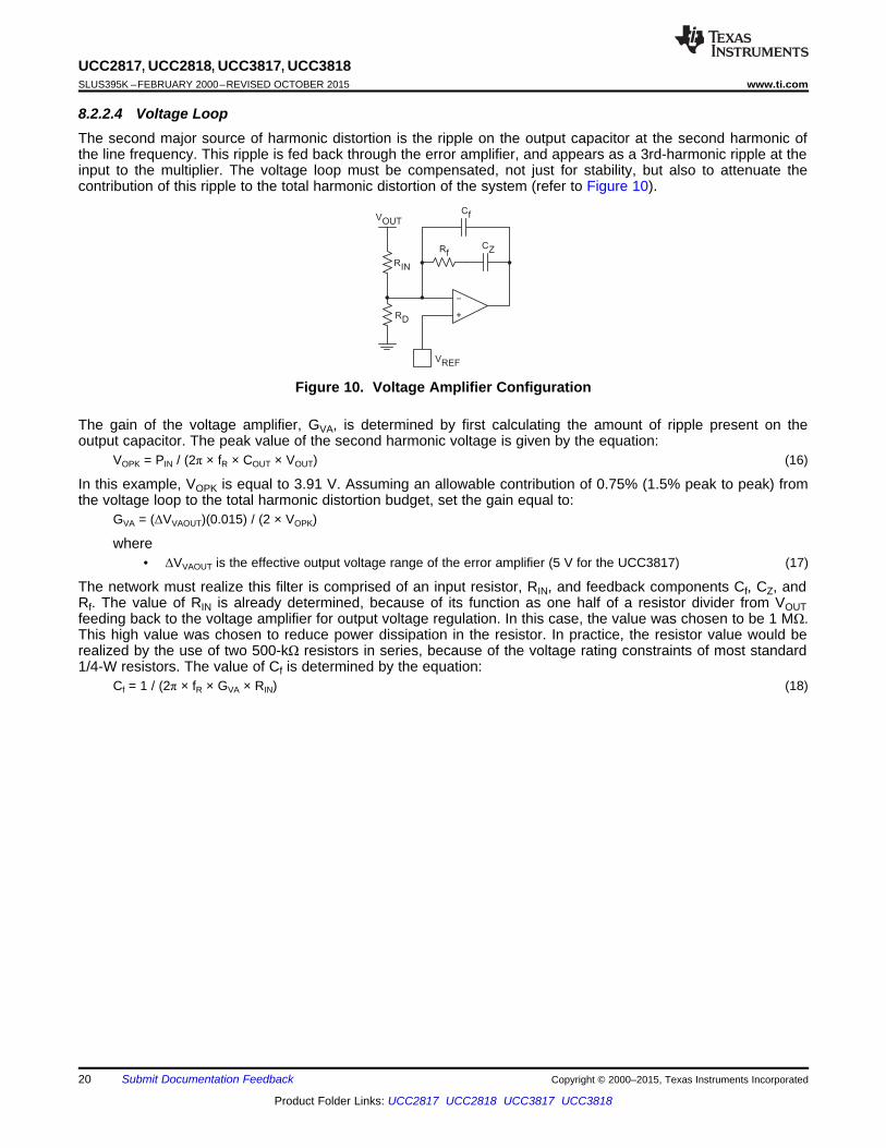
8.2.2.4 Voltage LoopThe second major source of harmonic distortion is the ripple on the output capacitor at the second harmonic ofthe line frequency. This ripple is fed back through the error amplifier, and appears as a 3rd-harmonic ripple at theinput to the multiplier. The voltage loop must be compensated, not just for stability, but also to attenuate thecontribution of this ripple to the total harmonic distortion of the system (refer to Figure 10).
Figure 10. Voltage Amplifier Configuration
The gain of the voltage amplifier, GVA, is determined by first calculating the amount of ripple present on theoutput capacitor. The peak value of the second harmonic voltage is given by the equation:
VOPK = PIN / (2π × fR × COUT × VOUT) (16)
In this example, VOPK is equal to 3.91 V. Assuming an allowable contribution of 0.75% (1.5% peak to peak) fromthe voltage loop to the total harmonic distortion budget, set the gain equal to:
GVA = (ΔVVAOUT)(0.015) / (2 × VOPK)
where• ΔVVAOUT is the effective output voltage range of the error amplifier (5 V for the UCC3817) (17)
The network must realize this filter is comprised of an input resistor, RIN, and feedback components Cf, CZ, andRf. The value of RIN is already determined, because of its function as one half of a resistor divider from VOUTfeeding back to the voltage amplifier for output voltage regulation. In this case, the value was chosen to be 1 MΩ.This high value was chosen to reduce power dissipation in the resistor. In practice, the resistor value would berealized by the use of two 500-kΩ resistors in series, because of the voltage rating constraints of most standard1/4-W resistors. The value of Cf is determined by the equation:
Cf = 1 / (2π × fR × GVA × RIN) (18)

CZ
1
2
fVI
10R
f
=
× π × ×
21
UCC2817, UCC2818, UCC3817, UCC3818www.ti.com SLUS395K –FEBRUARY 2000–REVISED OCTOBER 2015
Product Folder Links: UCC2817 UCC2818 UCC3817 UCC3818
Submit Documentation FeedbackCopyright © 2000–2015, Texas Instruments Incorporated
In this example, Cf equals 150 nF. Resistor Rf sets the dc gain of the error amplifier and thus determines thefrequency of the pole of the error amplifier. The location of the pole can be found by setting the gain of the loopequation to one, and solving for the crossover frequency. The frequency, expressed in terms of input power, canbe calculated by the equation:
fVI2 = PIN / (2π2 × ΔVVAOUT × VOUT × RIN × COUT × Cf) (19)
fVI for this converter is 10 Hz. A derivation of this equation can be found in the Unitrode Power Supply DesignSeminar SEM1000, Topic 1, [A 250-kHz, 500-W Power Factor Correction Circuit Employing Zero VoltageTransitions].
Solving for Rf becomes:Rf = 1 / (2π × fVI × Cf) (20)
or Rf equals 100 kΩ.
Due to the low output impedance of the voltage amplifier, capacitor CZ was added in series with RF to reduceloading on the voltage divider. To ensure the voltage loop crossed over at fVI, CZ was selected to add a zero at a10th of fVI. For the design in Figure 9, a 2.2-μF capacitor was chosen for CZ. The following equation can calculateCZ.
(21)

+
−+
−
RSENSE
+−
MULT
Zf
PWM
COMPARATORCA
QBOOST
LBOOST
VOUT
RI
+
−
Rf
CP
CAOUT
CZ
22
UCC2817, UCC2818, UCC3817, UCC3818SLUS395K –FEBRUARY 2000–REVISED OCTOBER 2015 www.ti.com
Product Folder Links: UCC2817 UCC2818 UCC3817 UCC3818
Submit Documentation Feedback Copyright © 2000–2015, Texas Instruments Incorporated
8.2.2.5 Current LoopThe gain of the power stage is:
GID(s) = (VOUT × RSENSE) / (s × LBOOST × VP) (22)
RSENSE has been chosen to give the desired differential voltage for the current sense amplifier at the desiredcurrent limit point. In this example, a current limit of 4 A and a reasonable differential voltage to the current ampof 1 V gives a RSENSE value of 0.25 Ω. VP in this equation is the voltage swing of the oscillator ramp, 4 V for theUCC3817. Setting the crossover frequency of the system to 1/10th of the switching frequency, or 10 kHz,requires a power stage gain at that frequency of 0.383. For the system to have a gain of 1 at the crossoverfrequency, the current amplifier must have a gain of 1/GID at that frequency. GEA, the current amplifier gain isthen:
GEA = (1/GID) = (1/0.383) = 2.611 (23)
RI is the RMOUT resistor, previously calculated to be 3.9 kΩ. (refer to Figure 11). The gain of the current amplifieris Rf/RI, so multiplying RI by GEA gives the value of Rf,which in this case is approximately 12 kΩ. Setting a zero atthe crossover frequency and a pole at half the switching frequency completes the current loop compensation.
CZ = 1 / (2 × π × Rf × fC) (24)CP = 1 / (2 × π × Rf × fS/2) (25)
Figure 11. Current Loop Compensation
The UCC3817 current amplifier has the input from the multiplier applied to the inverting input. This change inarchitecture from previous Texas Instruments PFC controllers improves noise immunity in the current amplifierand adds a phase inversion into the control loop. The UCC3817 takes advantage of this phase inversion toimplement leading-edge duty cycle modulation. Synchronizing a boost PFC controller to a downstream dc-to-dccontroller reduces the ripple current seen by the bulk capacitor between stages, reducing capacitor size and costand reducing EMI. This is explained in greater detail in Capacitor Ripple Reduction. The UCC3817 currentamplifier configuration is shown in Figure 12.
Figure 12. UCC3817 Current Amplifier Configuration

Output Power (W)
Pow
er F
acto
r
25 50 75 100 125 150 175 200 225 250 2750.4
0.48
0.56
0.64
0.72
0.8
0.88
0.96
1.04
1.12
1.2
D001
VIN = 85 VVIN = 175 VVIN = 265 V
Output Power
Effi
cien
cy (
%)
25 50 75 100 125 150 175 200 225 25075
80
85
90
95
100
D001
VIN = 85 VVIN = 175 VVIN = 265 V
23
UCC2817, UCC2818, UCC3817, UCC3818www.ti.com SLUS395K –FEBRUARY 2000–REVISED OCTOBER 2015
Product Folder Links: UCC2817 UCC2818 UCC3817 UCC3818
Submit Documentation FeedbackCopyright © 2000–2015, Texas Instruments Incorporated
8.2.2.6 Start UpThe UCC3818 version of the device is intended to have VCC connected to a 12-V supply voltage. The UCC3817has an internal shunt regulator, enabling the device to be powered from bootstrap circuitry as shown in Figure 9.The current drawn by the UCC3817 during undervoltage lockout, or start-up current, is typically 150 μA. OnceVCC is above the UVLO threshold, the device is enabled and draws 4 mA typically. A resistor connectedbetween the rectified ac line voltage and the VCC pin provides current to the shunt regulator during power up.Once the circuit is operational, the bootstrap winding of the inductor provides the VCC voltage. Sizing of thestart-up resistor is determined by the start-up time requirement of the system design.
IC = C(ΔV/Δt) (26)R = (VRMS × 0.9) / IC
where• IC is the charge current• C is the total capacitance at the VCC pin• ΔV is the UVLO threshold• Δt is the allowed start-up time (27)
Assuming a 1 second allowed start-up time, a 16-V VCC turn-on threshold, and a total VCC capacitance of 100μF, a resistor value of 51 kΩ is required at a low line input voltage of 85 VRMS. The IC start-up current issufficiently small as to be ignored in sizing the start-up resistor.
8.2.3 Application Curves
Figure 13. Efficiency vs Output PowerFigure 14. Power Factor vs Output Power

24
UCC2817, UCC2818, UCC3817, UCC3818SLUS395K –FEBRUARY 2000–REVISED OCTOBER 2015 www.ti.com
Product Folder Links: UCC2817 UCC2818 UCC3817 UCC3818
Submit Documentation Feedback Copyright © 2000–2015, Texas Instruments Incorporated
9 Power Supply Recommendations
9.1 Power Switch SelectionAs in any power supply design, tradeoffs between performance, cost, and size must be made. When selecting apower switch, calculate the total power dissipation in the switch for several different devices at the switchingfrequencies being considered for the converter. Total power dissipation in the switch is the sum of switching lossand conduction loss. Switching losses are the combination of the gate charge loss, COSS loss and turnon andturnoff losses:
PGATE = QGATE × VGATE × fS (28)PCOSS = 1/2 × COSS × V2
OFF × fS (29)PON + POFF = 1/2 × VOFF × IL × (tON + tOFF) × fS
where• QGATE is the total gate charge• VGATE is the gate drive voltage• fS is the clock frequency• COSS is the drain source capacitance of the MOSFET• IL is the peak inductor current• tON and tOFF are the switching times (estimated using device parameters RGATE, QGD and VTH)• VOFF is the voltage across the switch during the off time; in this case VOFF = VOUT (30)
Conduction loss is calculated as the product of the RDS(on) of the switch (at the worst case junction temperature)and the square of RMS current:
PCOND = RDS(on) × K × I2RMS
where• K is the temperature factor found in the manufacturer’s RDS(on) vs. junction temperature curves (31)
Calculating these losses and plotting against frequency gives a curve that enables the designer to determineeither which device has the best performance at the desired switching frequency, or which switching frequencyhas the least total loss for a particular power switch. For the design example in Figure 9, an IRFP450 HEXFETfrom International Rectifier was chosen because of its low RDS(on) and its VDSS rating. The IRFP450 RDS(on) of 0.4Ω and the maximum VDSS of 500 V made it an ideal choice. An excellent review of this procedure can be found inthe Unitrode Power Supply Design Seminar SEM1200, Topic 6, Design Review: 140 W, [Multiple Output HighDensity DC/DC Converter].

25
UCC2817, UCC2818, UCC3817, UCC3818www.ti.com SLUS395K –FEBRUARY 2000–REVISED OCTOBER 2015
Product Folder Links: UCC2817 UCC2818 UCC3817 UCC3818
Submit Documentation FeedbackCopyright © 2000–2015, Texas Instruments Incorporated
10 Layout
10.1 Layout Guidelines
10.1.1 Capacitor Ripple ReductionFor a power system where the PFC boost converter is followed by a dc-to-dc converter stage, it can be beneficialto synchronize the two converters. In addition to the usual advantages such as noise reduction and stability,proper synchronization can significantly reduce the ripple currents in the output capacitor of the boost circuit.Figure 15 helps illustrate the impact of proper synchronization, by showing a PFC boost converter together withthe simplified input stage of a forward converter.
The capacitor current during a single switching cycle depends on the status of the switches Q1 and Q2, and isshown in Figure 16. With a synchronization scheme that maintains conventional trailing-edge modulation on bothconverters, the capacitor current ripple is highest. The greatest ripple current cancellation is attained when theoverlap of Q1 offtime and Q2 ontime is maximized. One method of achieving this is to synchronize the turnon ofthe boost diode (D1) with the turnon of Q2. This approach implies that the leading edge of the boost converter ispulse-width modulated, while the forward converter is modulated with traditional trailing-edge PWM. TheUCC3817 is designed as a leading-edge modulator with easy synchronization to the downstream converter tofacilitate this advantage. Table 2 compares the ICB(rms) for D1/Q2 synchronization as offered by UCC3817 versusthe ICB(rms) for the other extreme of synchronizing the turnon of Q1 and Q2 for a 200-W power system with a VBSTof 385 V.
Figure 15. Simplified Representation of a 2-Stage PFC Power Supply

CT
RT
RT
CT
D2
D1
C1
Gate Drive
From Down
Stream PWM
UCC3817
26
UCC2817, UCC2818, UCC3817, UCC3818SLUS395K –FEBRUARY 2000–REVISED OCTOBER 2015 www.ti.com
Product Folder Links: UCC2817 UCC2818 UCC3817 UCC3818
Submit Documentation Feedback Copyright © 2000–2015, Texas Instruments Incorporated
Layout Guidelines (continued)
Figure 16. Timing Waveforms for Synchronization Scheme
Table 2. Effects of Synchronization on Boost Capacitor CurrentVIN = 85 V VIN = 120 V VIN = 240 V
D(Q2) Q1/Q2 D1/Q2 Q1/Q2 D1/Q2 Q1/Q2 D1/Q20.35 1.491 A 0.835 A 1.341 A 0.663 A 1.024 A 0.731 A0.45 1.432 A 0.93 A 1.276 A 0.664 A 0.897 A 0.614 A
Table 2 illustrates that the boost capacitor ripple current can be reduced by approximately 50% at nominal line,and about 30% at high line with the synchronization scheme facilitated by the UCC3817. Figure 17 shows thesuggested technique for synchronizing the UCC3817 to the downstream converter. With this technique,maximum ripple reduction as shown in Figure 16 is achievable. The output capacitance value can be significantlyreduced if its choice is dictated by ripple current, or the capacitor life can be increased as a result. In cost-sensitive designs where holdup time is not critical, this is a significant advantage.
An alternative method of synchronization makes it possible to achieve the same ripple reduction. In this method,the turnon of Q1 is synchronized to the turnoff of Q2. While this method yields almost identical ripple reductionand maintains trailing edge modulation on both converters, the synchronization is more difficult to achieve, andthe circuit can become susceptible to noise as the synchronizing edge itself is being modulated.
Figure 17. Synchronizing the UCC3817 to a Down-Stream Converter

R16R10
R9
R11
C9
C8
C10
C11
R21
R13
C2
C3U1
R5
R4
R3
R19
R2
R1
R20
SYNC
VCCR22
C1
C4
D4
C5
R6
R7
C14
C7
C15
C6
D5 D6
R8R12
FA1
UCC3817 EVALUATION BOARD
D3
AC1
XC12
AC2
C13
D8 L1
XL1
D7
R1
8
R1
5
D2
D1
V0
Q1
HS1
GND
C12
GND
R17
R14
HIGH TEMPERATURE - SEE
EVM WARNINGS AND
RESTRICTIONS
HIGH VOLTAGE -
SEE EVM WARNINGS AND
RESTRICTIONS
HIGH VOLTAGE -
SEE EVM WARNINGS AND
RESTRICTIONS
27
UCC2817, UCC2818, UCC3817, UCC3818www.ti.com SLUS395K –FEBRUARY 2000–REVISED OCTOBER 2015
Product Folder Links: UCC2817 UCC2818 UCC3817 UCC3818
Submit Documentation FeedbackCopyright © 2000–2015, Texas Instruments Incorporated
10.2 Layout Example
Figure 18. UCC3817EVM Evaluation Board Layout Assembly

28
UCC2817, UCC2818, UCC3817, UCC3818SLUS395K –FEBRUARY 2000–REVISED OCTOBER 2015 www.ti.com
Product Folder Links: UCC2817 UCC2818 UCC3817 UCC3818
Submit Documentation Feedback Copyright © 2000–2015, Texas Instruments Incorporated
11 Device and Documentation Support
11.1 Documentation Support
11.1.1 Related DocumentationFor related documentation see the following:1. Differences Between UCC3817A/18A/19A and UCC3817/18/19 (SLUA294)2. UCC3817 BiCMOS Power Factor Preregulator Evaluation Board (SLUU077)3. Synchronizing a PFC Controller from a Down Stream Controller Gate Drive (SLUA245)4. Seminar topic, High Power Factor Switching Preregulator Design Optimization, L.H. Dixon, SEM-700,1990.5. Seminar topic, High Power Factor Preregulator for Off-line Supplies, L.H. Dixon, SEM-600, 1988.
11.2 Related LinksThe table below lists quick access links. Categories include technical documents, support and communityresources, tools and software, and quick access to sample or buy.
Table 3. Related Links
PARTS PRODUCT FOLDER SAMPLE & BUY TECHNICALDOCUMENTS
TOOLS &SOFTWARE
SUPPORT &COMMUNITY
UCC2817 Click here Click here Click here Click here Click hereUCC2818 Click here Click here Click here Click here Click hereUC3817 Click here Click here Click here Click here Click hereUC3818 Click here Click here Click here Click here Click here
11.3 Receiving Notification of Documentation UpdatesTo receive notification of documentation updates, navigate to the device product folder on ti.com. In the upperright corner, click on Alert me to register and receive a weekly digest of any product information that haschanged. For change details, review the revision history included in any revised document.
11.4 Community ResourcesThe following links connect to TI community resources. Linked contents are provided "AS IS" by the respectivecontributors. They do not constitute TI specifications and do not necessarily reflect TI's views; see TI's Terms ofUse.
TI E2E™ Online Community TI's Engineer-to-Engineer (E2E) Community. Created to foster collaborationamong engineers. At e2e.ti.com, you can ask questions, share knowledge, explore ideas and helpsolve problems with fellow engineers.
Design Support TI's Design Support Quickly find helpful E2E forums along with design support tools andcontact information for technical support.
11.5 TrademarksE2E is a trademark of Texas Instruments.All other trademarks are the property of their respective owners.
11.6 Electrostatic Discharge CautionThese devices have limited built-in ESD protection. The leads should be shorted together or the device placed in conductive foamduring storage or handling to prevent electrostatic damage to the MOS gates.
11.7 GlossarySLYZ022 — TI Glossary.
This glossary lists and explains terms, acronyms, and definitions.

29
UCC2817, UCC2818, UCC3817, UCC3818www.ti.com SLUS395K –FEBRUARY 2000–REVISED OCTOBER 2015
Product Folder Links: UCC2817 UCC2818 UCC3817 UCC3818
Submit Documentation FeedbackCopyright © 2000–2015, Texas Instruments Incorporated
12 Mechanical, Packaging, and Orderable InformationThe following pages include mechanical, packaging, and orderable information. This information is the mostcurrent data available for the designated devices. This data is subject to change without notice and revision ofthis document. For browser-based versions of this data sheet, refer to the left-hand navigation.

PACKAGE OPTION ADDENDUM
www.ti.com 23-Aug-2017
Addendum-Page 1
PACKAGING INFORMATION
Orderable Device Status(1)
Package Type PackageDrawing
Pins PackageQty
Eco Plan(2)
Lead/Ball Finish(6)
MSL Peak Temp(3)
Op Temp (°C) Device Marking(4/5)
Samples
UCC2817D ACTIVE SOIC D 16 40 Green (RoHS& no Sb/Br)
CU NIPDAU Level-1-260C-UNLIM -40 to 85 UCC2817D
UCC2817DG4 ACTIVE SOIC D 16 40 Green (RoHS& no Sb/Br)
CU NIPDAU Level-1-260C-UNLIM -40 to 85 UCC2817D
UCC2817DTR ACTIVE SOIC D 16 2500 Green (RoHS& no Sb/Br)
CU NIPDAU Level-1-260C-UNLIM -40 to 85 UCC2817D
UCC2817DTRG4 ACTIVE SOIC D 16 2500 Green (RoHS& no Sb/Br)
CU NIPDAU Level-1-260C-UNLIM -40 to 85 UCC2817D
UCC2817DW ACTIVE SOIC DW 16 40 Green (RoHS& no Sb/Br)
CU NIPDAU Level-2-260C-1 YEAR -40 to 85 UCC2817DW
UCC2817DWG4 ACTIVE SOIC DW 16 40 Green (RoHS& no Sb/Br)
CU NIPDAU Level-2-260C-1 YEAR -40 to 85 UCC2817DW
UCC2817N ACTIVE PDIP N 16 25 Green (RoHS& no Sb/Br)
CU NIPDAU N / A for Pkg Type -40 to 85 UCC2817N
UCC2818D ACTIVE SOIC D 16 40 Green (RoHS& no Sb/Br)
CU NIPDAU Level-1-260C-UNLIM -40 to 85 UCC2818D
UCC2818DG4 ACTIVE SOIC D 16 40 Green (RoHS& no Sb/Br)
CU NIPDAU Level-1-260C-UNLIM -40 to 85 UCC2818D
UCC2818DTR ACTIVE SOIC D 16 2500 Green (RoHS& no Sb/Br)
CU NIPDAU Level-1-260C-UNLIM -40 to 85 UCC2818D
UCC2818DTRG4 ACTIVE SOIC D 16 2500 Green (RoHS& no Sb/Br)
CU NIPDAU Level-1-260C-UNLIM -40 to 85 UCC2818D
UCC2818DW ACTIVE SOIC DW 16 40 Green (RoHS& no Sb/Br)
CU NIPDAU Level-2-260C-1 YEAR -40 to 85 UCC2818DW
UCC2818DWG4 ACTIVE SOIC DW 16 40 Green (RoHS& no Sb/Br)
CU NIPDAU Level-2-260C-1 YEAR -40 to 85 UCC2818DW
UCC2818DWTR ACTIVE SOIC DW 16 2000 Green (RoHS& no Sb/Br)
CU NIPDAU Level-2-260C-1 YEAR -40 to 85 UCC2818DW
UCC2818DWTRG4 ACTIVE SOIC DW 16 2000 Green (RoHS& no Sb/Br)
CU NIPDAU Level-2-260C-1 YEAR -40 to 85 UCC2818DW
UCC2818N ACTIVE PDIP N 16 25 Green (RoHS& no Sb/Br)
CU NIPDAU N / A for Pkg Type -40 to 85 UCC2818N
UCC2818NG4 ACTIVE PDIP N 16 25 Green (RoHS& no Sb/Br)
CU NIPDAU N / A for Pkg Type -40 to 85 UCC2818N

PACKAGE OPTION ADDENDUM
www.ti.com 23-Aug-2017
Addendum-Page 2
Orderable Device Status(1)
Package Type PackageDrawing
Pins PackageQty
Eco Plan(2)
Lead/Ball Finish(6)
MSL Peak Temp(3)
Op Temp (°C) Device Marking(4/5)
Samples
UCC2818PW ACTIVE TSSOP PW 16 90 Green (RoHS& no Sb/Br)
CU NIPDAU Level-2-260C-1 YEAR -40 to 85 2818PW
UCC3817D ACTIVE SOIC D 16 40 Green (RoHS& no Sb/Br)
CU NIPDAU Level-1-260C-UNLIM 0 to 70 UCC3817D
UCC3817DG4 ACTIVE SOIC D 16 40 Green (RoHS& no Sb/Br)
CU NIPDAU Level-1-260C-UNLIM 0 to 70 UCC3817D
UCC3817DTR ACTIVE SOIC D 16 2500 Green (RoHS& no Sb/Br)
CU NIPDAU Level-1-260C-UNLIM 0 to 70 UCC3817D
UCC3817DTRG4 ACTIVE SOIC D 16 2500 Green (RoHS& no Sb/Br)
CU NIPDAU Level-1-260C-UNLIM 0 to 70 UCC3817D
UCC3817DW ACTIVE SOIC DW 16 40 Green (RoHS& no Sb/Br)
CU NIPDAU Level-2-260C-1 YEAR 0 to 70 UCC3817DW
UCC3817DWG4 ACTIVE SOIC DW 16 40 Green (RoHS& no Sb/Br)
CU NIPDAU Level-2-260C-1 YEAR 0 to 70 UCC3817DW
UCC3817DWTR ACTIVE SOIC DW 16 2000 Green (RoHS& no Sb/Br)
CU NIPDAU Level-2-260C-1 YEAR 0 to 70 UCC3817DW
UCC3817N ACTIVE PDIP N 16 25 Green (RoHS& no Sb/Br)
CU NIPDAU N / A for Pkg Type 0 to 70 UCC3817N
UCC3817NG4 ACTIVE PDIP N 16 25 Green (RoHS& no Sb/Br)
CU NIPDAU N / A for Pkg Type 0 to 70 UCC3817N
UCC3818D ACTIVE SOIC D 16 40 Green (RoHS& no Sb/Br)
CU NIPDAU Level-1-260C-UNLIM 0 to 70 UCC3818D
UCC3818DG4 ACTIVE SOIC D 16 40 Green (RoHS& no Sb/Br)
CU NIPDAU Level-1-260C-UNLIM 0 to 70 UCC3818D
UCC3818DTR ACTIVE SOIC D 16 2500 Green (RoHS& no Sb/Br)
CU NIPDAU Level-1-260C-UNLIM 0 to 70 UCC3818D
UCC3818DTRG4 ACTIVE SOIC D 16 2500 Green (RoHS& no Sb/Br)
CU NIPDAU Level-1-260C-UNLIM 0 to 70 UCC3818D
UCC3818DW ACTIVE SOIC DW 16 40 Green (RoHS& no Sb/Br)
CU NIPDAU Level-2-260C-1 YEAR 0 to 70 UCC3818DW
UCC3818DWTR ACTIVE SOIC DW 16 2000 Green (RoHS& no Sb/Br)
CU NIPDAU Level-2-260C-1 YEAR 0 to 70 UCC3818DW
UCC3818DWTRG4 ACTIVE SOIC DW 16 2000 Green (RoHS& no Sb/Br)
CU NIPDAU Level-2-260C-1 YEAR 0 to 70 UCC3818DW
UCC3818N ACTIVE PDIP N 16 25 Green (RoHS& no Sb/Br)
CU NIPDAU N / A for Pkg Type 0 to 70 UCC3818N

PACKAGE OPTION ADDENDUM
www.ti.com 23-Aug-2017
Addendum-Page 3
Orderable Device Status(1)
Package Type PackageDrawing
Pins PackageQty
Eco Plan(2)
Lead/Ball Finish(6)
MSL Peak Temp(3)
Op Temp (°C) Device Marking(4/5)
Samples
UCC3818NG4 ACTIVE PDIP N 16 25 Green (RoHS& no Sb/Br)
CU NIPDAU N / A for Pkg Type 0 to 70 UCC3818N
UCC3818PW ACTIVE TSSOP PW 16 90 Green (RoHS& no Sb/Br)
CU NIPDAU Level-2-260C-1 YEAR 0 to 70 3818PW
(1) The marketing status values are defined as follows:ACTIVE: Product device recommended for new designs.LIFEBUY: TI has announced that the device will be discontinued, and a lifetime-buy period is in effect.NRND: Not recommended for new designs. Device is in production to support existing customers, but TI does not recommend using this part in a new design.PREVIEW: Device has been announced but is not in production. Samples may or may not be available.OBSOLETE: TI has discontinued the production of the device.
(2) RoHS: TI defines "RoHS" to mean semiconductor products that are compliant with the current EU RoHS requirements for all 10 RoHS substances, including the requirement that RoHS substancedo not exceed 0.1% by weight in homogeneous materials. Where designed to be soldered at high temperatures, "RoHS" products are suitable for use in specified lead-free processes. TI mayreference these types of products as "Pb-Free".RoHS Exempt: TI defines "RoHS Exempt" to mean products that contain lead but are compliant with EU RoHS pursuant to a specific EU RoHS exemption.Green: TI defines "Green" to mean the content of Chlorine (Cl) and Bromine (Br) based flame retardants meet JS709B low halogen requirements of <=1000ppm threshold. Antimony trioxide basedflame retardants must also meet the <=1000ppm threshold requirement.
(3) MSL, Peak Temp. - The Moisture Sensitivity Level rating according to the JEDEC industry standard classifications, and peak solder temperature.
(4) There may be additional marking, which relates to the logo, the lot trace code information, or the environmental category on the device.
(5) Multiple Device Markings will be inside parentheses. Only one Device Marking contained in parentheses and separated by a "~" will appear on a device. If a line is indented then it is a continuationof the previous line and the two combined represent the entire Device Marking for that device.
(6) Lead/Ball Finish - Orderable Devices may have multiple material finish options. Finish options are separated by a vertical ruled line. Lead/Ball Finish values may wrap to two lines if the finishvalue exceeds the maximum column width.
Important Information and Disclaimer:The information provided on this page represents TI's knowledge and belief as of the date that it is provided. TI bases its knowledge and belief on informationprovided by third parties, and makes no representation or warranty as to the accuracy of such information. Efforts are underway to better integrate information from third parties. TI has taken andcontinues to take reasonable steps to provide representative and accurate information but may not have conducted destructive testing or chemical analysis on incoming materials and chemicals.TI and TI suppliers consider certain information to be proprietary, and thus CAS numbers and other limited information may not be available for release.
In no event shall TI's liability arising out of such information exceed the total purchase price of the TI part(s) at issue in this document sold by TI to Customer on an annual basis.
OTHER QUALIFIED VERSIONS OF UCC2818 :

PACKAGE OPTION ADDENDUM
www.ti.com 23-Aug-2017
Addendum-Page 4
• Enhanced Product: UCC2818-EP
NOTE: Qualified Version Definitions:
• Enhanced Product - Supports Defense, Aerospace and Medical Applications

TAPE AND REEL INFORMATION
*All dimensions are nominal
Device PackageType
PackageDrawing
Pins SPQ ReelDiameter
(mm)
ReelWidth
W1 (mm)
A0(mm)
B0(mm)
K0(mm)
P1(mm)
W(mm)
Pin1Quadrant
UCC2817DTR SOIC D 16 2500 330.0 16.4 6.5 10.3 2.1 8.0 16.0 Q1
UCC2818DTR SOIC D 16 2500 330.0 16.4 6.5 10.3 2.1 8.0 16.0 Q1
UCC2818DWTR SOIC DW 16 2000 330.0 16.4 10.75 10.7 2.7 12.0 16.0 Q1
UCC3817DTR SOIC D 16 2500 330.0 16.4 6.5 10.3 2.1 8.0 16.0 Q1
UCC3817DWTR SOIC DW 16 2000 330.0 16.4 10.75 10.7 2.7 12.0 16.0 Q1
UCC3818DTR SOIC D 16 2500 330.0 16.4 6.5 10.3 2.1 8.0 16.0 Q1
UCC3818DWTR SOIC DW 16 2000 330.0 16.4 10.75 10.7 2.7 12.0 16.0 Q1
PACKAGE MATERIALS INFORMATION
www.ti.com 24-Aug-2017
Pack Materials-Page 1
*All dimensions are nominal
Device Package Type Package Drawing Pins SPQ Length (mm) Width (mm) Height (mm)
UCC2817DTR SOIC D 16 2500 333.2 345.9 28.6
UCC2818DTR SOIC D 16 2500 333.2 345.9 28.6
UCC2818DWTR SOIC DW 16 2000 367.0 367.0 38.0
UCC3817DTR SOIC D 16 2500 333.2 345.9 28.6
UCC3817DWTR SOIC DW 16 2000 367.0 367.0 38.0
UCC3818DTR SOIC D 16 2500 333.2 345.9 28.6
UCC3818DWTR SOIC DW 16 2000 367.0 367.0 38.0
PACKAGE MATERIALS INFORMATION
www.ti.com 24-Aug-2017
Pack Materials-Page 2


GENERIC PACKAGE VIEW
Images above are just a representation of the package family, actual package may vary.Refer to the product data sheet for package details.
DW 16 SOIC - 2.65 mm max heightSMALL OUTLINE INTEGRATED CIRCUIT
4040000-2/H

www.ti.com
PACKAGE OUTLINE
C
TYP10.639.97
2.65 MAX
14X 1.27
16X 0.510.31
2X8.89
TYP0.330.10
0 - 80.30.1
(1.4)
0.25GAGE PLANE
1.270.40
A
NOTE 3
10.510.1
BNOTE 4
7.67.4
4220721/A 07/2016
SOIC - 2.65 mm max heightDW0016ASOIC
NOTES: 1. All linear dimensions are in millimeters. Dimensions in parenthesis are for reference only. Dimensioning and tolerancing per ASME Y14.5M. 2. This drawing is subject to change without notice. 3. This dimension does not include mold flash, protrusions, or gate burrs. Mold flash, protrusions, or gate burrs shall not exceed 0.15 mm, per side. 4. This dimension does not include interlead flash. Interlead flash shall not exceed 0.25 mm, per side.5. Reference JEDEC registration MS-013.
1 16
0.25 C A B
98
PIN 1 IDAREA
SEATING PLANE
0.1 C
SEE DETAIL A
DETAIL ATYPICAL
SCALE 1.500

www.ti.com
EXAMPLE BOARD LAYOUT
0.07 MAXALL AROUND
0.07 MINALL AROUND
(9.3)
14X (1.27)
R0.05 TYP
16X (2)
16X (0.6)
4220721/A 07/2016
SOIC - 2.65 mm max heightDW0016ASOIC
NOTES: (continued) 6. Publication IPC-7351 may have alternate designs. 7. Solder mask tolerances between and around signal pads can vary based on board fabrication site.
METAL SOLDER MASKOPENING
NON SOLDER MASKDEFINED
SOLDER MASK DETAILS
OPENINGSOLDER MASK METAL
SOLDER MASKDEFINED
LAND PATTERN EXAMPLESCALE:7X
SYMM
1
8 9
16
SEEDETAILS
SYMM

www.ti.com
EXAMPLE STENCIL DESIGN
R0.05 TYP
16X (2)
16X (0.6)
14X (1.27)
(9.3)
4220721/A 07/2016
SOIC - 2.65 mm max heightDW0016ASOIC
NOTES: (continued) 8. Laser cutting apertures with trapezoidal walls and rounded corners may offer better paste release. IPC-7525 may have alternate design recommendations. 9. Board assembly site may have different recommendations for stencil design.
SOLDER PASTE EXAMPLEBASED ON 0.125 mm THICK STENCIL
SCALE:7X
SYMM
SYMM
1
8 9
16


IMPORTANT NOTICE
Texas Instruments Incorporated (TI) reserves the right to make corrections, enhancements, improvements and other changes to itssemiconductor products and services per JESD46, latest issue, and to discontinue any product or service per JESD48, latest issue. Buyersshould obtain the latest relevant information before placing orders and should verify that such information is current and complete.TI’s published terms of sale for semiconductor products (http://www.ti.com/sc/docs/stdterms.htm) apply to the sale of packaged integratedcircuit products that TI has qualified and released to market. Additional terms may apply to the use or sale of other types of TI products andservices.Reproduction of significant portions of TI information in TI data sheets is permissible only if reproduction is without alteration and isaccompanied by all associated warranties, conditions, limitations, and notices. TI is not responsible or liable for such reproduceddocumentation. Information of third parties may be subject to additional restrictions. Resale of TI products or services with statementsdifferent from or beyond the parameters stated by TI for that product or service voids all express and any implied warranties for theassociated TI product or service and is an unfair and deceptive business practice. TI is not responsible or liable for any such statements.Buyers and others who are developing systems that incorporate TI products (collectively, “Designers”) understand and agree that Designersremain responsible for using their independent analysis, evaluation and judgment in designing their applications and that Designers havefull and exclusive responsibility to assure the safety of Designers' applications and compliance of their applications (and of all TI productsused in or for Designers’ applications) with all applicable regulations, laws and other applicable requirements. Designer represents that, withrespect to their applications, Designer has all the necessary expertise to create and implement safeguards that (1) anticipate dangerousconsequences of failures, (2) monitor failures and their consequences, and (3) lessen the likelihood of failures that might cause harm andtake appropriate actions. Designer agrees that prior to using or distributing any applications that include TI products, Designer willthoroughly test such applications and the functionality of such TI products as used in such applications.TI’s provision of technical, application or other design advice, quality characterization, reliability data or other services or information,including, but not limited to, reference designs and materials relating to evaluation modules, (collectively, “TI Resources”) are intended toassist designers who are developing applications that incorporate TI products; by downloading, accessing or using TI Resources in anyway, Designer (individually or, if Designer is acting on behalf of a company, Designer’s company) agrees to use any particular TI Resourcesolely for this purpose and subject to the terms of this Notice.TI’s provision of TI Resources does not expand or otherwise alter TI’s applicable published warranties or warranty disclaimers for TIproducts, and no additional obligations or liabilities arise from TI providing such TI Resources. TI reserves the right to make corrections,enhancements, improvements and other changes to its TI Resources. TI has not conducted any testing other than that specificallydescribed in the published documentation for a particular TI Resource.Designer is authorized to use, copy and modify any individual TI Resource only in connection with the development of applications thatinclude the TI product(s) identified in such TI Resource. NO OTHER LICENSE, EXPRESS OR IMPLIED, BY ESTOPPEL OR OTHERWISETO ANY OTHER TI INTELLECTUAL PROPERTY RIGHT, AND NO LICENSE TO ANY TECHNOLOGY OR INTELLECTUAL PROPERTYRIGHT OF TI OR ANY THIRD PARTY IS GRANTED HEREIN, including but not limited to any patent right, copyright, mask work right, orother intellectual property right relating to any combination, machine, or process in which TI products or services are used. Informationregarding or referencing third-party products or services does not constitute a license to use such products or services, or a warranty orendorsement thereof. Use of TI Resources may require a license from a third party under the patents or other intellectual property of thethird party, or a license from TI under the patents or other intellectual property of TI.TI RESOURCES ARE PROVIDED “AS IS” AND WITH ALL FAULTS. TI DISCLAIMS ALL OTHER WARRANTIES ORREPRESENTATIONS, EXPRESS OR IMPLIED, REGARDING RESOURCES OR USE THEREOF, INCLUDING BUT NOT LIMITED TOACCURACY OR COMPLETENESS, TITLE, ANY EPIDEMIC FAILURE WARRANTY AND ANY IMPLIED WARRANTIES OFMERCHANTABILITY, FITNESS FOR A PARTICULAR PURPOSE, AND NON-INFRINGEMENT OF ANY THIRD PARTY INTELLECTUALPROPERTY RIGHTS. TI SHALL NOT BE LIABLE FOR AND SHALL NOT DEFEND OR INDEMNIFY DESIGNER AGAINST ANY CLAIM,INCLUDING BUT NOT LIMITED TO ANY INFRINGEMENT CLAIM THAT RELATES TO OR IS BASED ON ANY COMBINATION OFPRODUCTS EVEN IF DESCRIBED IN TI RESOURCES OR OTHERWISE. IN NO EVENT SHALL TI BE LIABLE FOR ANY ACTUAL,DIRECT, SPECIAL, COLLATERAL, INDIRECT, PUNITIVE, INCIDENTAL, CONSEQUENTIAL OR EXEMPLARY DAMAGES INCONNECTION WITH OR ARISING OUT OF TI RESOURCES OR USE THEREOF, AND REGARDLESS OF WHETHER TI HAS BEENADVISED OF THE POSSIBILITY OF SUCH DAMAGES.Unless TI has explicitly designated an individual product as meeting the requirements of a particular industry standard (e.g., ISO/TS 16949and ISO 26262), TI is not responsible for any failure to meet such industry standard requirements.Where TI specifically promotes products as facilitating functional safety or as compliant with industry functional safety standards, suchproducts are intended to help enable customers to design and create their own applications that meet applicable functional safety standardsand requirements. Using products in an application does not by itself establish any safety features in the application. Designers mustensure compliance with safety-related requirements and standards applicable to their applications. Designer may not use any TI products inlife-critical medical equipment unless authorized officers of the parties have executed a special contract specifically governing such use.Life-critical medical equipment is medical equipment where failure of such equipment would cause serious bodily injury or death (e.g., lifesupport, pacemakers, defibrillators, heart pumps, neurostimulators, and implantables). Such equipment includes, without limitation, allmedical devices identified by the U.S. Food and Drug Administration as Class III devices and equivalent classifications outside the U.S.TI may expressly designate certain products as completing a particular qualification (e.g., Q100, Military Grade, or Enhanced Product).Designers agree that it has the necessary expertise to select the product with the appropriate qualification designation for their applicationsand that proper product selection is at Designers’ own risk. Designers are solely responsible for compliance with all legal and regulatoryrequirements in connection with such selection.Designer will fully indemnify TI and its representatives against any damages, costs, losses, and/or liabilities arising out of Designer’s non-compliance with the terms and provisions of this Notice.
Mailing Address: Texas Instruments, Post Office Box 655303, Dallas, Texas 75265Copyright © 2017, Texas Instruments Incorporated