ua78l00 series positive-voltage linear regulators
TRANSCRIPT
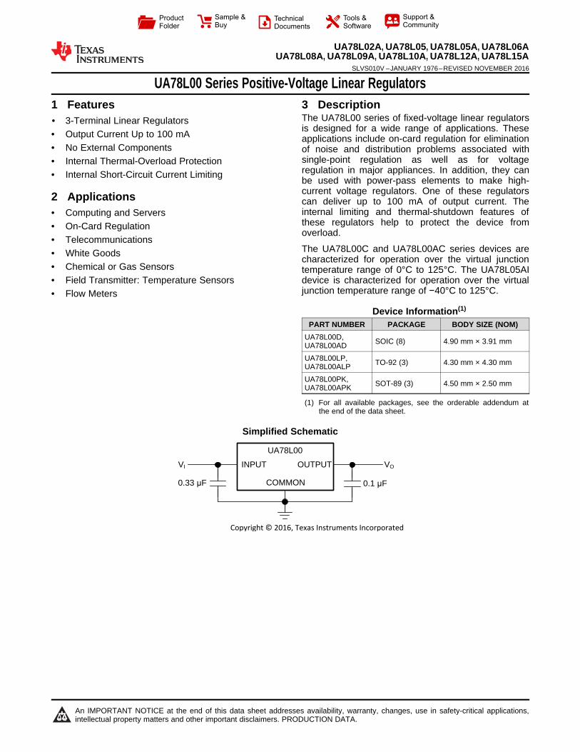
INPUT OUTPUT
COMMON
UA78L00
0.1 �F0.33 �F
VI VO
Copyright © 2016, Texas Instruments Incorporated
Product
Folder
Sample &Buy
Technical
Documents
Tools &
Software
Support &Community
An IMPORTANT NOTICE at the end of this data sheet addresses availability, warranty, changes, use in safety-critical applications,intellectual property matters and other important disclaimers. PRODUCTION DATA.
UA78L02A, UA78L05, UA78L05A, UA78L06AUA78L08A, UA78L09A, UA78L10A, UA78L12A, UA78L15A
SLVS010V –JANUARY 1976–REVISED NOVEMBER 2016
UA78L00 Series Positive-Voltage Linear Regulators
1
1 Features1• 3-Terminal Linear Regulators• Output Current Up to 100 mA• No External Components• Internal Thermal-Overload Protection• Internal Short-Circuit Current Limiting
2 Applications• Computing and Servers• On-Card Regulation• Telecommunications• White Goods• Chemical or Gas Sensors• Field Transmitter: Temperature Sensors• Flow Meters
3 DescriptionThe UA78L00 series of fixed-voltage linear regulatorsis designed for a wide range of applications. Theseapplications include on-card regulation for eliminationof noise and distribution problems associated withsingle-point regulation as well as for voltageregulation in major appliances. In addition, they canbe used with power-pass elements to make high-current voltage regulators. One of these regulatorscan deliver up to 100 mA of output current. Theinternal limiting and thermal-shutdown features ofthese regulators help to protect the device fromoverload.
The UA78L00C and UA78L00AC series devices arecharacterized for operation over the virtual junctiontemperature range of 0°C to 125°C. The UA78L05AIdevice is characterized for operation over the virtualjunction temperature range of −40°C to 125°C.
Device Information(1)
PART NUMBER PACKAGE BODY SIZE (NOM)UA78L00D,UA78L00AD SOIC (8) 4.90 mm × 3.91 mm
UA78L00LP,UA78L00ALP TO-92 (3) 4.30 mm × 4.30 mm
UA78L00PK,UA78L00APK SOT-89 (3) 4.50 mm × 2.50 mm
(1) For all available packages, see the orderable addendum atthe end of the data sheet.
Simplified Schematic
2
UA78L02A, UA78L05, UA78L05A, UA78L06AUA78L08A, UA78L09A, UA78L10A, UA78L12A, UA78L15ASLVS010V –JANUARY 1976–REVISED NOVEMBER 2016 www.ti.com
Product Folder Links: UA78L02A UA78L05 UA78L05A UA78L06A UA78L08A UA78L09A UA78L10A UA78L12AUA78L15A
Submit Documentation Feedback Copyright © 1976–2016, Texas Instruments Incorporated
Table of Contents1 Features .................................................................. 12 Applications ........................................................... 13 Description ............................................................. 14 Revision History..................................................... 25 Pin Configuration and Functions ......................... 36 Specifications......................................................... 4
6.1 Absolute Maximum Ratings ...................................... 46.2 ESD Ratings.............................................................. 46.3 Recommended Operating Conditions....................... 46.4 Thermal Information .................................................. 46.5 Electrical Characteristics: UA78L02.......................... 56.6 Electrical Characteristics: UA78L05.......................... 56.7 Electrical Characteristics: UA78L06.......................... 66.8 Electrical Characteristics: UA78L08.......................... 66.9 Electrical Characteristics: UA78L09.......................... 76.10 Electrical Characteristics: UA78L10........................ 76.11 Electrical Characteristics: UA78L12........................ 86.12 Electrical Characteristics: UA78L15........................ 86.13 Typical Characteristics ............................................ 9
7 Detailed Description ............................................ 10
7.1 Overview ................................................................. 107.2 Functional Block Diagram ....................................... 107.3 Feature Description................................................. 107.4 Device Functional Modes........................................ 10
8 Applications and Implementation ...................... 118.1 Application Information............................................ 118.2 Typical Application ................................................. 118.3 System Examples ................................................... 12
9 Power Supply Recommendations ...................... 1310 Layout................................................................... 13
10.1 Layout Guidelines ................................................. 1310.2 Layout Example .................................................... 13
11 Device and Documentation Support ................. 1411.1 Related Links ........................................................ 1411.2 Receiving Notification of Documentation Updates 1411.3 Community Resource............................................ 1411.4 Trademarks ........................................................... 1411.5 Electrostatic Discharge Caution............................ 1411.6 Glossary ................................................................ 14
12 Mechanical, Packaging, and OrderableInformation ........................................................... 14
4 Revision HistoryNOTE: Page numbers for previous revisions may differ from page numbers in the current version.
Changes from Revision U (January 2014) to Revision V Page
• Added Device Information table, ESD Ratings table, Feature Description section, Device Functional Modes,Application and Implementation section, Power Supply Recommendations section, Layout section, Device andDocumentation Support section, and Mechanical, Packaging, and Orderable Information section....................................... 1
• Added Applications ................................................................................................................................................................. 1• Changed θJA values in Thermal Information table From: 97 To: 115 (D), From: 140 To: 143.6 (LP), and From: 52 To:
54.7 (PK)................................................................................................................................................................................. 4• Changed θJC values in Thermal Information table From: 39 To: 60.3 (D), From: 55 To: 74.4 (LP), and From: 9 To:
88.1 (PK)................................................................................................................................................................................. 4
Changes from Revision T (May 2011) to Revision U Page
• Deleted Ordering Information table; see Product Option Addendum at the end of the data sheet........................................ 1• Updated document to new TI data sheet format - no specification changes ......................................................................... 1
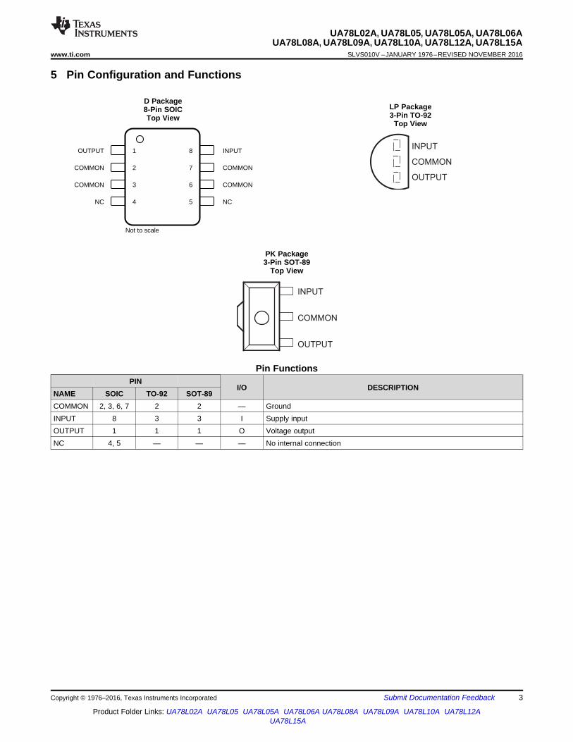
INPUT
COMMON
OUTPUT
1OUTPUT 8 INPUT
2COMMON 7 COMMON
3COMMON 6 COMMON
4NC 5 NC
Not to scale
INPUT
COMMON
OUTPUT
3
UA78L02A, UA78L05, UA78L05A, UA78L06AUA78L08A, UA78L09A, UA78L10A, UA78L12A, UA78L15A
www.ti.com SLVS010V –JANUARY 1976–REVISED NOVEMBER 2016
Product Folder Links: UA78L02A UA78L05 UA78L05A UA78L06A UA78L08A UA78L09A UA78L10A UA78L12AUA78L15A
Submit Documentation FeedbackCopyright © 1976–2016, Texas Instruments Incorporated
5 Pin Configuration and Functions
D Package8-Pin SOICTop View
LP Package3-Pin TO-92
Top View
PK Package3-Pin SOT-89
Top View
Pin FunctionsPIN
I/O DESCRIPTIONNAME SOIC TO-92 SOT-89COMMON 2, 3, 6, 7 2 2 — GroundINPUT 8 3 3 I Supply inputOUTPUT 1 1 1 O Voltage outputNC 4, 5 — — — No internal connection

4
UA78L02A, UA78L05, UA78L05A, UA78L06AUA78L08A, UA78L09A, UA78L10A, UA78L12A, UA78L15ASLVS010V –JANUARY 1976–REVISED NOVEMBER 2016 www.ti.com
Product Folder Links: UA78L02A UA78L05 UA78L05A UA78L06A UA78L08A UA78L09A UA78L10A UA78L12AUA78L15A
Submit Documentation Feedback Copyright © 1976–2016, Texas Instruments Incorporated
(1) Stresses beyond those listed under Absolute Maximum Ratings may cause permanent damage to the device. These are stress ratingsonly, and functional operation of the device at these or any other conditions beyond those indicated under Recommended OperatingConditions is not implied. Exposure to absolute-maximum-rated conditions for extended periods may affect device reliability.
6 Specifications
6.1 Absolute Maximum Ratingsover operating free-air temperature range (unless otherwise noted) (1)
MIN MAX UNIT
Input voltage, VIUA78L02AC, UA78L05C, UA78L09C, and UA78L10AC 30
VUA78L12C, UA78L12AC, UA78L15C, and UA78L15AC 35
Virtual junction temperature, TJ 150 °CStorage temperature, Tstg –65 150 °C
(1) JEDEC document JEP155 states that 500-V HBM allows safe manufacturing with a standard ESD control process.(2) JEDEC document JEP157 states that 250-V CDM allows safe manufacturing with a standard ESD control process.
6.2 ESD RatingsVALUE UNIT
V(ESD) Electrostatic dischargeHuman body model (HBM), per ANSI/ESDA/JEDEC JS-001, all pins (1) 1000
VCharged device model (CDM), per JEDEC specification JESD22-C101, allpins (2) 1000
6.3 Recommended Operating ConditionsMIN MAX UNIT
VI Input voltage
UA78L02AC 4.75 20
V
UA78L05C and UA78L05AC 7 20UA78L06C and UA78L06AC 8.5 20UA78L08C and UA78L08AC 10.5 23UA78L09C and UA78L09AC 11.5 24UA78L10AC 12.5 25UA78L12C and UA78L12AC 14.5 27UA78L15C and UA78L15AC 17.5 30
IO Output current 100 mA
TJ Operating virtual junction temperatureUA78L00C and UA78L00AC series 0 125
°CUA78L05AI –40 125
(1) For more information about traditional and new thermal metrics, see the Semiconductor and IC Package Thermal Metrics applicationreport.
6.4 Thermal Information
THERMAL METRIC (1)UA78L00
UNITD (SOIC) LP (TO-92) PK (SOT-89)8 PINS 3 PINS 3 PINS
RθJA Junction-to-ambient thermal resistance 115 143.6 54.7 °C/WRθJC(top) Junction-to-case (top) thermal resistance 60.3 74.4 88.1 °C/WRθJB Junction-to-board thermal resistance 55.6 — 9.6 °C/WψJT Junction-to-top characterization parameter 16.2 24.2 6.2 °C/WψJB Junction-to-board characterization parameter 55 120.9 9.7 °C/WRθJC(bot) Junction-to-case (bottom) thermal resistance — — 7.7 °C/W

5
UA78L02A, UA78L05, UA78L05A, UA78L06AUA78L08A, UA78L09A, UA78L10A, UA78L12A, UA78L15A
www.ti.com SLVS010V –JANUARY 1976–REVISED NOVEMBER 2016
Product Folder Links: UA78L02A UA78L05 UA78L05A UA78L06A UA78L08A UA78L09A UA78L10A UA78L12AUA78L15A
Submit Documentation FeedbackCopyright © 1976–2016, Texas Instruments Incorporated
(1) Applies to UA78L02AC.(2) Pulse-testing techniques maintain TJ as close to TA as possible. Thermal effects must be taken into account separately. All
characteristics are measured with a 0.33-µF capacitor across the input and a 0.1-µF capacitor across the output.
6.5 Electrical Characteristics: UA78L02at specified virtual junction temperature, VI = 9 V, and IO = 40 mA (unless otherwise noted) (1)
PARAMETER TEST CONDITIONS (2) MIN TYP MAX UNIT
Output voltagefVI = 4.75 V to 20 V, and IO = 1 mA to 40 mA
TJ = 25°C 2.5 2.6 2.7VTJ = 0°C to 125°C 2.45 2.75
IO = 1 mA to 70 mA, and TJ = 0°C to 125°C 2.45 2.75
Input voltage regulationVI = 4.75 V to 20 V, and TJ = 25°C 20 100
mVVI = 5 V to 20 V, and TJ = 25°C 16 75
Ripple rejection VI = 6 V to 20 V, f = 120 Hz, and TJ = 25°C 43 51 dB
Output voltage regulationIO = 1 mA to 100 mA, and TJ = 25°C 12 50
mVIO = 1 mA to 40 mA, and TJ = 25°C 6 25
Output noise voltage f = 10 Hz to 100 kHz, and TJ = 25°C 30 µVDropout voltage TJ = 25°C 1.7 V
Bias currentTJ = 25°C 3.6 6
mATJ = 125°C 5.5
Bias current changeVI = 5 V to 20 V, and TJ = 0°C to 125°C 2.5
mAIO = 1 mA to 40 mA, and TJ = 0°C to 125°C 0.1
(1) Pulse-testing techniques maintain TJ as close to TA as possible. Thermal effects must be taken into account separately. Allcharacteristics are measured with a 0.33-μF capacitor across the input and a 0.1-μF capacitor across the output. Full range for theUA78L05AC is TJ = 0°C to 125°C, and full range for the UA78L05AI is TJ = –40°C to 125°C.
6.6 Electrical Characteristics: UA78L05at specified virtual junction temperature, VI = 10 V, and IO = 40 mA (unless otherwise noted)
PARAMETER TEST CONDITIONS (1) MIN TYP MAX UNIT
Output voltage
VI = 7 V to 20 V, andIO = 1 mA to 40 mA
TJ = 25°CUA78L05C 4.6 5 5.4
V
UA78L05AC andUA78L05AI 4.8 5 5.2
TJ = full rangeUA78L05C 4.5 5.5UA78L05AC andUA78L05AI 4.75 5.25
IO = 1 mA to 70 mA, andTJ = full range
UA78L05C 4.5 5.5UA78L05AC and UA78L05AI 4.75 5.25
Input voltageregulation
VI = 7 V to 20 V, andTJ = 25°C
UA78L05C 32 200
mVUA78L05AC and UA78L05AI 32 150
VI = 8 V to 20 V, andTJ = 25°C
UA78L05C 26 150UA78L05AC and UA78L05AI 26 100
Ripple rejection VI = 8 V to 18 V, f = 120 Hz,and TJ = 25°C
UA78L05C 40 49dB
UA78L05AC and UA78L05AI 41 49
Output voltageregulation
IO = 1 mA to 100 mA, and TJ = 25°C 15 60mV
IO = 1 mA to 40 mA, and TJ = 25°C 8 30Output noise voltage f = 10 Hz to 100 kHz, and TJ = 25°C 42 μVDropout voltage TJ = 25°C 1.7 V
Bias currentTJ = 25°C 3.8 6
mATJ = 125°C 5.5
Bias current changeVI = 8 V to 20 V, and TJ = full range 1.5
mAIO = 1 mA to 40 mA, andTJ = full range
UA78L05C 0.2UA78L05AC and UA78L05AI 0.1
6
UA78L02A, UA78L05, UA78L05A, UA78L06AUA78L08A, UA78L09A, UA78L10A, UA78L12A, UA78L15ASLVS010V –JANUARY 1976–REVISED NOVEMBER 2016 www.ti.com
Product Folder Links: UA78L02A UA78L05 UA78L05A UA78L06A UA78L08A UA78L09A UA78L10A UA78L12AUA78L15A
Submit Documentation Feedback Copyright © 1976–2016, Texas Instruments Incorporated
(1) Pulse-testing techniques maintain TJ as close to TA as possible. Thermal effects must be taken into account separately. Allcharacteristics are measured with a 0.33-µF capacitor across the input and a 0.1-µF capacitor across the output.
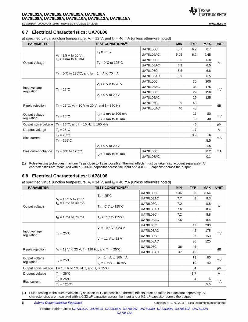
6.7 Electrical Characteristics: UA78L06at specified virtual junction temperature, VI = 12 V, and IO = 40 mA (unless otherwise noted)
PARAMETER TEST CONDITIONS (1) MIN TYP MAX UNIT
Output voltage
VI = 8.5 V to 20 V,IO = 1 mA to 40 mA
TJ = 25°CUA78L06C 5.7 6.2 6.7
V
UA78L06AC 5.95 6.2 6.45
TJ = 0°C to 125°CUA78L06C 5.6 6.8UA78L06AC 5.9 6.5
TJ = 0°C to 125°C, and IO = 1 mA to 70 mAUA78L06C 5.6 6.8UA78L06AC 5.9 6.5
Input voltageregulation TJ = 25°C
VI = 8.5 V to 20 VUA78L06C 35 200
mVUA78L06AC 35 175
VI = 9 V to 20 VUA78L06C 29 150UA78L06AC 29 125
Ripple rejection TJ = 25°C, VI = 10 V to 20 V, and f = 120 HzUA78L06C 39 48
dBUA78L06AC 40 48
Output voltageregulation TJ = 25°C
IO = 1 mA to 100 mA 16 80mV
IO = 1 mA to 40 mA 9 40Output noise voltage TJ = 25°C, and f = 10 Hz to 100 kHz 46 µVDropout voltage TJ = 25°C 1.7 V
Bias currentTJ = 25°C 3.9 6
mATJ = 125°C 5.5
Bias current change TJ = 0°C to 125°CVI = 9 V to 20 V 1.5
mAIO = 1 mA to 40 mA
UA78L06C 0.2UA78L06AC 0.1
(1) Pulse-testing techniques maintain TJ as close to TA as possible. Thermal effects must be taken into account separately. Allcharacteristics are measured with a 0.33-µF capacitor across the input and a 0.1-µF capacitor across the output.
6.8 Electrical Characteristics: UA78L08at specified virtual junction temperature, VI = 14 V, and IO = 40 mA (unless otherwise noted)
PARAMETER TEST CONDITIONS (1) MIN TYP MAX UNIT
Output voltage
VI = 10.5 V to 23 V,IO = 1 mA to 40 mA
TJ = 25°CUA78L08C 7.36 8 8.64
V
UA78L08AC 7.7 8 8.3
TJ = 0°C to 125°CUA78L08C 7.2 8.8UA78L08AC 7.6 8.4
IO = 1 mA to 70 mA TJ = 0°C to 125°CUA78L08C 7.2 8.8UA78L08AC 7.6 8.4
Input voltageregulation TJ = 25°C
VI = 10.5 V to 23 VUA78L08C 42 200
mVUA78L08AC 42 175
VI = 11 V to 23 VUA78L08C 36 150UA78L08AC 36 125
Ripple rejection VI = 13 V to 23 V, f = 120 Hz, and TJ = 25°CUA78L08C 36 46
dBUA78L08AC 37 46
Output voltageregulation TJ = 25°C
IO = 1 mA to 100 mA 18 80mV
IO = 1 mA to 40 mA 10 40Output noise voltage f = 10 Hz to 100 kHz, and TJ = 25°C 54 µVDropout voltage TJ = 25°C 1.7 V
Bias currentTJ = 25°C 4 6
mATJ = 125°C 5.5
7
UA78L02A, UA78L05, UA78L05A, UA78L06AUA78L08A, UA78L09A, UA78L10A, UA78L12A, UA78L15A
www.ti.com SLVS010V –JANUARY 1976–REVISED NOVEMBER 2016
Product Folder Links: UA78L02A UA78L05 UA78L05A UA78L06A UA78L08A UA78L09A UA78L10A UA78L12AUA78L15A
Submit Documentation FeedbackCopyright © 1976–2016, Texas Instruments Incorporated
Electrical Characteristics: UA78L08 (continued)at specified virtual junction temperature, VI = 14 V, and IO = 40 mA (unless otherwise noted)
PARAMETER TEST CONDITIONS (1) MIN TYP MAX UNIT
Bias current change TJ = 0°C to 125°CVI = 11 V to 23 V 1.5
mAIO = 1 mA to 40 mA
UA78L08C 0.2UA78L08AC 0.1
(1) Pulse-testing techniques maintain TJ as close to TA as possible. Thermal effects must be taken into account separately. Allcharacteristics are measured with a 0.33-µF capacitor across the input and a 0.1-µF capacitor across the output.
6.9 Electrical Characteristics: UA78L09at specified virtual junction temperature, VI = 16 V, and IO = 40 mA (unless otherwise noted)
PARAMETER TEST CONDITIONS (1) MIN TYP MAX UNIT
Output voltage
VI = 12 V to 24 V,IO = 1 mA to 40 mA
TJ = 25°CUA78L09C 8.3 9 9.7
V
UA78L09AC 8.6 9 9.4
TJ = 0°C to 125°CUA78L09C 8.1 9.9UA78L09AC 8.55 9.45
IO = 1 mA to 70 mA, and TJ = 0°C to 125°CUA78L09C 8.1 9.9UA78L09AC 8.55 9.45
Input voltageregulation TJ = 25°C
VI = 12 V to 24 VUA78L09C 45 225
mVUA78L09AC 45 175
VI = 13 V to 24 VUA78L09C 40 175UA78L09AC 40 125
Ripple rejection VI = 15 V to 25 V, f = 120 Hz, and TJ = 25°CUA78L09C 36 45
dBUA78L09AC 38 45
Output voltageregulation TJ = 25°C
IO = 1 mA to 100 mA 19 90mV
IO = 1 mA to 40 mA 11 40Output noise voltage f = 10 Hz to 100 kHz, and TJ = 25°C 58 µVDropout voltage TJ = 25°C 1.7 V
Bias currentTJ = 25°C 4.1 6
mATJ = 125°C 5.5
Bias current change TJ = 0°C to 125°CVI = 13 V to 24 V 1.5
mAIO = 1 mA to 40 mA
UA78L09C 0.2UA78L09AC 0.1
(1) Applies to UA78L10AC.(2) Pulse-testing techniques maintain TJ as close to TA as possible. Thermal effects must be taken into account separately. All
characteristics are measured with a 0.33-µF capacitor across the input and a 0.1-µF capacitor across the output.
6.10 Electrical Characteristics: UA78L10at specified virtual junction temperature, VI = 14 V, and IO = 40 mA (unless otherwise noted) (1)
PARAMETER TEST CONDITIONS (2) MIN TYP MAX UNIT
Output voltageVI = 13 V to 25 V, and IO =1 mA to 40 mA
TJ = 25°C 9.6 10 10.4VTJ = 0°C to 125°C 9.5 10.5
TJ = 0°C to 125°C, and IO = 1 mA to 70 mA 9.5 10.5
Input voltage regulation TJ = 25°CVI = 13 V to 25 V 51 175
mVVI = 14 V to 25 V 42 125
Ripple rejection TJ = 25°C, VI = 15 V to 25 V, and f = 120 Hz 37 44 dB
Output voltage regulation TJ = 25°CIO = 1 mA to 100 mA 20 90
mVIO = 1 mA to 40 mA 11 40
Output noise voltage TJ = 25°C, and f = 10 Hz to 100 kHz 62 µVDropout voltage TJ = 25°C 1.7 V

8
UA78L02A, UA78L05, UA78L05A, UA78L06AUA78L08A, UA78L09A, UA78L10A, UA78L12A, UA78L15ASLVS010V –JANUARY 1976–REVISED NOVEMBER 2016 www.ti.com
Product Folder Links: UA78L02A UA78L05 UA78L05A UA78L06A UA78L08A UA78L09A UA78L10A UA78L12AUA78L15A
Submit Documentation Feedback Copyright © 1976–2016, Texas Instruments Incorporated
Electrical Characteristics: UA78L10 (continued)at specified virtual junction temperature, VI = 14 V, and IO = 40 mA (unless otherwise noted)(1)
PARAMETER TEST CONDITIONS (2) MIN TYP MAX UNIT
Bias currentTJ = 25°C 4.2 6
mATJ = 125°C 5.5
Bias current change TJ = 0°C to 125°CVI = 14 V to 25 V 1.5
mAIO = 1 mA to 40 mA 0.1
(1) Pulse-testing techniques maintain TJ as close to TA as possible. Thermal effects must be taken into account separately. Allcharacteristics are measured with a 0.33-µF capacitor across the input and a 0.1-µF capacitor across the output.
6.11 Electrical Characteristics: UA78L12at specified virtual junction temperature, VI = 19 V, and IO = 40 mA (unless otherwise noted)
PARAMETER TEST CONDITIONS (1) MIN TYP MAX UNIT
Output voltage
VI = 14 V to 27 V, andIO = 1 mA to 40 mA
TJ = 25°CUA78L12C 11.1 12 12.9
V
UA78L12AC 11.5 12 12.5
TJ = 0°C to 125°CUA78L12C 10.8 13.2UA78L12AC 11.4 12.6
TJ = 0°C to 125°C, and IO = 1 mA to 70 mAUA78L12C 10.8 13.2UA78L12AC 11.4 12.6
Input voltage regulation TJ = 25°CVI = 14.5 V to 27 V 55 250
mVVI = 16 V to 27 V 49 200
Ripple rejection TJ = 25°C VI = 15 V to 25 V, and f= 120 Hz
UA78L12C 36 42dB
UA78L12AC 37 42
Output voltage regulation TJ = 25°CIO = 1 mA to 100 mA 22 100
mVIO = 1 mA to 40 mA 13 50
Output noise voltage TJ = 25°C, and f = 10 Hz to 100 kHz 70 µVDropout voltage TJ = 25°C 1.7 V
Bias currentTJ = 25°C 4.3 6.5
mATJ = 125°C 6
Bias current change TJ = 0°C to 125°CVI = 16 V to 27 V 1.5
mAIO = 1 mA to 40 mA
UA78L12C 0.2UA78L12AC 0.1
(1) Pulse-testing techniques maintain TJ as close to TA as possible. Thermal effects must be taken into account separately. Allcharacteristics are measured with a 0.33-µF capacitor across the input and a 0.1-µF capacitor across the output.
6.12 Electrical Characteristics: UA78L15at specified virtual junction temperature, VI = 23 V, and IO = 40 mA (unless otherwise noted)
PARAMETER TEST CONDITIONS (1) MIN TYP MAX UNIT
Output voltage
VI = 17.5 V to 30 V,and IO = 1 mA to 40mA
TJ = 25°CUA78L15C 13.8 15 16.2
V
UA78L15AC 14.4 15 15.6
TJ = 0°C to 125°CUA78L15C 13.5 16.5UA78L15AC 14.25 15.75
TJ = 0°C to 125°C, and IO = 1 mA to 70 mAUA78L15C 13.5 16.5UA78L15AC 14.25 15.75
Input voltage regulation TJ = 25°CVI = 17.5 V to 30 V 65 300
mVVI = 20 V to 30 V 58 250
Ripple rejection TJ = 25°C VI = 18.5 V to 28.5 V,and f = 120 Hz
UA78L15C 33 39dB
UA78L15AC 34 39
Input Voltage (VI) [V]
Out
put V
olta
ge (
VO
) [V
]
6 8 10 12 14 16 18 204.9
4.92
4.94
4.96
4.98
5
5.02
5.04
5.06
5.08
5.1
D003
TA = 25qCIO = 40 mA
Output Current (IO) [mA]
Out
put V
olta
ge (
VO
) [V
]
0 10 20 30 40 50 60 70 80 90 1004.9
4.92
4.94
4.96
4.98
5
5.02
5.04
5.06
5.08
5.1
D004
TA = 25qCVI = 10 V
Load Current (IO) [mA]
Bia
s C
urre
nt [m
A]
0 10 20 30 40 50 60 70 80 90 1004.16
4.162
4.164
4.166
4.168
4.17
4.172
4.174
D001
TA = 25qCVI = 10 V
Input Voltage (VI) [V]
Bia
s C
urre
nt [m
A]
8 10 12 14 16 18 203.75
4
4.25
4.5
4.75
5
5.25
D002
TA = 25qCIO = 40 mA
9
UA78L02A, UA78L05, UA78L05A, UA78L06AUA78L08A, UA78L09A, UA78L10A, UA78L12A, UA78L15A
www.ti.com SLVS010V –JANUARY 1976–REVISED NOVEMBER 2016
Product Folder Links: UA78L02A UA78L05 UA78L05A UA78L06A UA78L08A UA78L09A UA78L10A UA78L12AUA78L15A
Submit Documentation FeedbackCopyright © 1976–2016, Texas Instruments Incorporated
Electrical Characteristics: UA78L15 (continued)at specified virtual junction temperature, VI = 23 V, and IO = 40 mA (unless otherwise noted)
PARAMETER TEST CONDITIONS (1) MIN TYP MAX UNIT
Output voltage regulation TJ = 25°CIO = 1 mA to 100 mA 25 150
mVIO = 1 mA to 40 mA 15 75
Output noise voltage TJ = 25°C, and f = 10 Hz to 100 kHz 82 μVDropout voltage TJ = 25°C 1.7 V
Bias currentTJ = 25°C 4.6 6.5
mATJ = 125°C 6
Bias current change TJ = 0°C to 125°CVI = 10 V to 30 V 1.5
mAIO = 1 mA to 40 mA
UA78L15C 0.2UA78L15AC 0.1
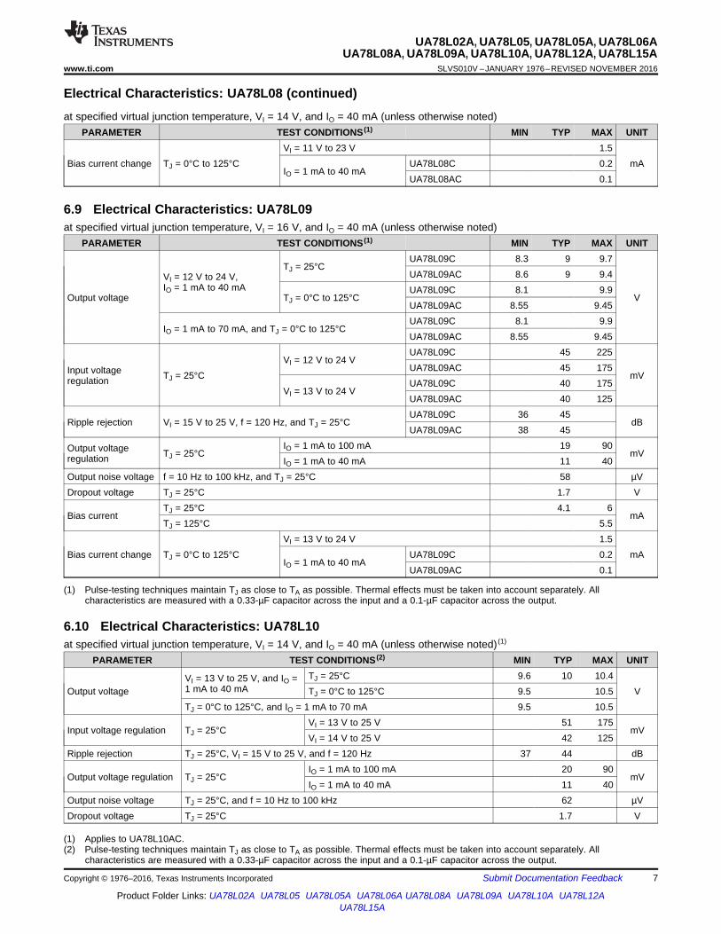
6.13 Typical Characteristics
Figure 1. Bias Current vs Load Current Figure 2. Bias Current vs Input Voltage
Figure 3. Line Regulation Figure 4. Load Regulation
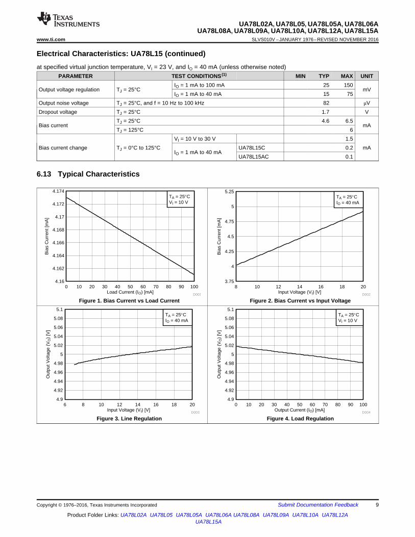
20 kW
INPUT
OUTPUT
COMMON
1 k to 14 kW W
1.4 kW
Copyright © 2016, Texas Instruments Incorporated
10
UA78L02A, UA78L05, UA78L05A, UA78L06AUA78L08A, UA78L09A, UA78L10A, UA78L12A, UA78L15ASLVS010V –JANUARY 1976–REVISED NOVEMBER 2016 www.ti.com
Product Folder Links: UA78L02A UA78L05 UA78L05A UA78L06A UA78L08A UA78L09A UA78L10A UA78L12AUA78L15A
Submit Documentation Feedback Copyright © 1976–2016, Texas Instruments Incorporated
7 Detailed Description
7.1 OverviewThe UA78L00 series of fixed-voltage integrated-circuit voltage regulators is designed for a wide range ofapplications. Each of these regulators can deliver up to 100 mA of output current at a fixed output voltagedepending on the device variant.
7.2 Functional Block Diagram
NOTE: Resistor values shown are nominal.
7.3 Feature DescriptionThe UA78L00 series of linear regulators are easy-to-use, fixed-output voltage regulators. The devices enable upto 100 mA of current and feature short-circuit current limiting and thermal overload protection.
7.4 Device Functional Modes
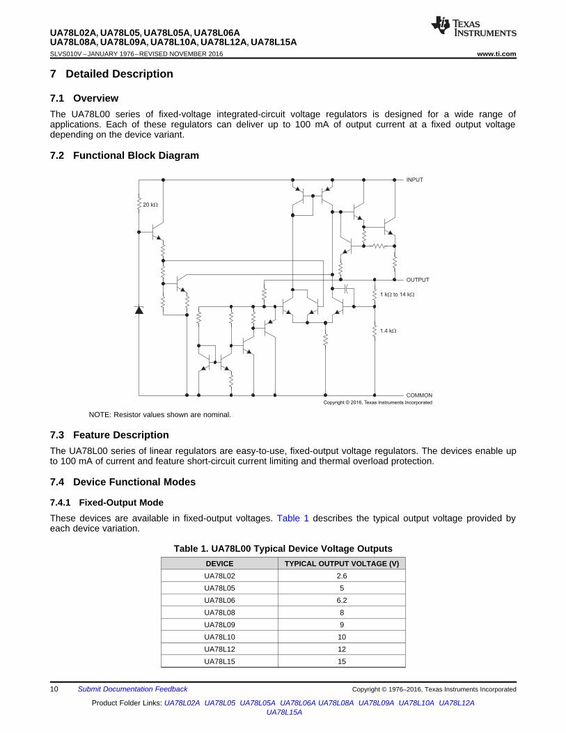
7.4.1 Fixed-Output ModeThese devices are available in fixed-output voltages. Table 1 describes the typical output voltage provided byeach device variation.
Table 1. UA78L00 Typical Device Voltage OutputsDEVICE TYPICAL OUTPUT VOLTAGE (V)UA78L02 2.6UA78L05 5UA78L06 6.2UA78L08 8UA78L09 9UA78L10 10UA78L12 12UA78L15 15

INPUT OUTPUT
COMMON
UA78L00
0.1 �F0.33 �F
VI VO
1N4001 or Equivalent
Copyright © 2016, Texas Instruments Incorporated
INPUT OUTPUT
COMMON
UA78L00
0.1 �F0.33 �F
VI VO
Copyright © 2016, Texas Instruments Incorporated
11
UA78L02A, UA78L05, UA78L05A, UA78L06AUA78L08A, UA78L09A, UA78L10A, UA78L12A, UA78L15A
www.ti.com SLVS010V –JANUARY 1976–REVISED NOVEMBER 2016
Product Folder Links: UA78L02A UA78L05 UA78L05A UA78L06A UA78L08A UA78L09A UA78L10A UA78L12AUA78L15A
Submit Documentation FeedbackCopyright © 1976–2016, Texas Instruments Incorporated
8 Applications and Implementation
NOTEInformation in the following applications sections is not part of the TI componentspecification, and TI does not warrant its accuracy or completeness. TI’s customers areresponsible for determining suitability of components for their purposes. Customers shouldvalidate and test their design implementation to confirm system functionality.
8.1 Application InformationThe UA78L00 devices are ideal for use as linear regulators with only a few external components needed. TheUA78L00 devices can also be used to clean power supply noise by attenuating ripple on the input signal.
8.2 Typical ApplicationThe UA78L00 devices are typically used as fixed-output linear regulators, sourcing current up to 100 mA into aload.
Figure 5. Fixed Output Regulator
8.2.1 Design RequirementsThe COMMON pin must be tied to ground to set the OUTPUT pin to the desired fixed output voltage.
Although not required, a 0.33-µF bypass capacitor is recommended on the input, and a 0.1-µF bypass capacitoris recommend on the output.
8.2.2 Detailed Design ProcedureOccasionally, the input voltage to the regulator can collapse faster than the output voltage. For example, this canoccur when the input supply is crowbarred during an output overvoltage condition. If the output voltage is greaterthan approximately 7 V, the emitter-base junction of the series-pass element (internal or external) could breakdown and be damaged. To prevent this, a diode shunt can be employed as shown in Figure 6.
Figure 6. Reverse-Bias-Protection Circuit

OO O
VI I Bias Current
R1
æ ö= +ç ÷
è ø
INPUT OUTPUT
COMMON
UA78L00
VI
GND
-VO
+
-
Copyright © 2016, Texas Instruments Incorporated
Input Voltage (VO) [V]
Out
put V
olta
ge (
VO
) [V
]
0 2 4 6 8 10 12 14 16 18 200
1
2
3
4
5
6
7
D005
TA = 25qCVO = 40 mA (@ 5V)
INPUT OUTPUT
COMMON
UA78L00
0.1 �F0.33 �F
VI VO
1N4001 or Equivalent
-VO
Copyright © 2016, Texas Instruments Incorporated
12
UA78L02A, UA78L05, UA78L05A, UA78L06AUA78L08A, UA78L09A, UA78L10A, UA78L12A, UA78L15ASLVS010V –JANUARY 1976–REVISED NOVEMBER 2016 www.ti.com
Product Folder Links: UA78L02A UA78L05 UA78L05A UA78L06A UA78L08A UA78L09A UA78L10A UA78L12AUA78L15A
Submit Documentation Feedback Copyright © 1976–2016, Texas Instruments Incorporated
Typical Application (continued)In many cases, a regulator powers a load that is not connected to ground, but instead, is connected to a voltagesource of opposite polarity (for example, operational amplifiers, level-shifting circuits, and so on). In these cases,a clamp diode should be connected to the regulator output as shown in Figure 7. This protects the regulator fromoutput polarity reversals during startup and short-circuit operation.
Figure 7. Output Polarity-Reversal-Protection Circuit
8.2.3 Application Curves
Figure 8. Output Voltage vs Input Voltage
8.3 System Examples
8.3.1 Positive Regulator in Negative Configuration
Figure 9. Positive Regulator in Negative Configuration (VI Must Float)
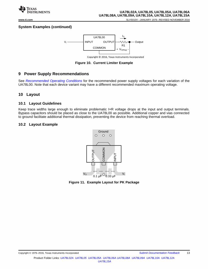
8.3.2 Current Limiter CircuitFigure 10 shows an example of using the UA78L00 as a current limiter. The output current limit is set byEquation 1.
(1)
OU
TP
UT
INP
UT
CO
MM
ON
0.1 �F 0.33 �FVIVO
Ground
INPUT OUTPUT
COMMON
UA78L00
VI Output
IO
R1VO(Reg)+ -
Copyright © 2016, Texas Instruments Incorporated
13
UA78L02A, UA78L05, UA78L05A, UA78L06AUA78L08A, UA78L09A, UA78L10A, UA78L12A, UA78L15A
www.ti.com SLVS010V –JANUARY 1976–REVISED NOVEMBER 2016
Product Folder Links: UA78L02A UA78L05 UA78L05A UA78L06A UA78L08A UA78L09A UA78L10A UA78L12AUA78L15A
Submit Documentation FeedbackCopyright © 1976–2016, Texas Instruments Incorporated
System Examples (continued)
Figure 10. Current Limiter Example
9 Power Supply RecommendationsSee Recommended Operating Conditions for the recommended power supply voltages for each variation of theUA78L00. Note that each device variant may have a different recommended maximum operating voltage.
10 Layout
10.1 Layout GuidelinesKeep trace widths large enough to eliminate problematic I×R voltage drops at the input and output terminals.Bypass capacitors should be placed as close to the UA78L00 as possible. Additional copper and vias connectedto ground facilitate additional thermal dissipation, preventing the device from reaching thermal overload.
10.2 Layout Example
Figure 11. Example Layout for PK Package

14
UA78L02A, UA78L05, UA78L05A, UA78L06AUA78L08A, UA78L09A, UA78L10A, UA78L12A, UA78L15ASLVS010V –JANUARY 1976–REVISED NOVEMBER 2016 www.ti.com
Product Folder Links: UA78L02A UA78L05 UA78L05A UA78L06A UA78L08A UA78L09A UA78L10A UA78L12AUA78L15A
Submit Documentation Feedback Copyright © 1976–2016, Texas Instruments Incorporated
11 Device and Documentation Support
11.1 Related LinksThe table below lists quick access links. Categories include technical documents, support and communityresources, tools and software, and quick access to sample or buy.
Table 2. Related Links
PARTS PRODUCT FOLDER SAMPLE & BUY TECHNICALDOCUMENTS
TOOLS &SOFTWARE
SUPPORT &COMMUNITY
UA78L02A Click here Click here Click here Click here Click hereUA78L05 Click here Click here Click here Click here Click here
UA78L05A Click here Click here Click here Click here Click hereUA78L06A Click here Click here Click here Click here Click hereUA78L08A Click here Click here Click here Click here Click hereUA78L09A Click here Click here Click here Click here Click hereUA78L10A Click here Click here Click here Click here Click hereUA78L12A Click here Click here Click here Click here Click hereUA78L15A Click here Click here Click here Click here Click here
11.2 Receiving Notification of Documentation UpdatesTo receive notification of documentation updates, navigate to the device product folder on ti.com. In the upperright corner, click on Alert me to register and receive a weekly digest of any product information that haschanged. For change details, review the revision history included in any revised document.
11.3 Community ResourceThe following links connect to TI community resources. Linked contents are provided "AS IS" by the respectivecontributors. They do not constitute TI specifications and do not necessarily reflect TI's views; see TI's Terms ofUse.
TI E2E™ Online Community TI's Engineer-to-Engineer (E2E) Community. Created to foster collaborationamong engineers. At e2e.ti.com, you can ask questions, share knowledge, explore ideas and helpsolve problems with fellow engineers.
Design Support TI's Design Support Quickly find helpful E2E forums along with design support tools andcontact information for technical support.
11.4 TrademarksE2E is a trademark of Texas Instruments.All other trademarks are the property of their respective owners.
11.5 Electrostatic Discharge CautionThese devices have limited built-in ESD protection. The leads should be shorted together or the device placed in conductive foamduring storage or handling to prevent electrostatic damage to the MOS gates.
11.6 GlossarySLYZ022 — TI Glossary.
This glossary lists and explains terms, acronyms, and definitions.
12 Mechanical, Packaging, and Orderable InformationThe following pages include mechanical, packaging, and orderable information. This information is the mostcurrent data available for the designated devices. This data is subject to change without notice and revision ofthis document. For browser-based versions of this data sheet, refer to the left-hand navigation.

PACKAGE OPTION ADDENDUM
www.ti.com 10-Mar-2022
Addendum-Page 1
PACKAGING INFORMATION
Orderable Device Status(1)
Package Type PackageDrawing
Pins PackageQty
Eco Plan(2)
Lead finish/Ball material
(6)
MSL Peak Temp(3)
Op Temp (°C) Device Marking(4/5)
Samples
UA78L02ACD ACTIVE SOIC D 8 75 RoHS & Green NIPDAU Level-1-260C-UNLIM 0 to 125 78L02A
UA78L02ACDG4 ACTIVE SOIC D 8 75 RoHS & Green NIPDAU Level-1-260C-UNLIM 0 to 125 78L02A
UA78L02ACLP ACTIVE TO-92 LP 3 1000 RoHS & Green SN N / A for Pkg Type 0 to 125 78L02AC
UA78L02ACLPE3 ACTIVE TO-92 LP 3 1000 RoHS & Green SN N / A for Pkg Type 0 to 125 78L02AC
UA78L05ACD ACTIVE SOIC D 8 75 RoHS & Green NIPDAU Level-1-260C-UNLIM 0 to 125 78L05A
UA78L05ACDE4 ACTIVE SOIC D 8 75 RoHS & Green NIPDAU Level-1-260C-UNLIM 0 to 125 78L05A
UA78L05ACDG4 ACTIVE SOIC D 8 75 RoHS & Green NIPDAU Level-1-260C-UNLIM 0 to 125 78L05A
UA78L05ACDR ACTIVE SOIC D 8 2500 RoHS & Green NIPDAU | SN Level-1-260C-UNLIM 0 to 125 78L05A
UA78L05ACDRE4 ACTIVE SOIC D 8 2500 RoHS & Green NIPDAU Level-1-260C-UNLIM 0 to 125 78L05A
UA78L05ACDRG4 ACTIVE SOIC D 8 2500 RoHS & Green NIPDAU Level-1-260C-UNLIM 0 to 125 78L05A
UA78L05ACLP ACTIVE TO-92 LP 3 1000 RoHS & Green SN N / A for Pkg Type 0 to 125 78L05AC
UA78L05ACLPE3 ACTIVE TO-92 LP 3 1000 RoHS & Green SN N / A for Pkg Type 0 to 125 78L05AC
UA78L05ACLPM ACTIVE TO-92 LP 3 2000 RoHS & Green SN N / A for Pkg Type 0 to 125 78L05AC
UA78L05ACLPME3 ACTIVE TO-92 LP 3 2000 RoHS & Green SN N / A for Pkg Type 0 to 125 78L05AC
UA78L05ACLPR ACTIVE TO-92 LP 3 2000 RoHS & Green SN N / A for Pkg Type 0 to 125 78L05AC
UA78L05ACLPRE3 ACTIVE TO-92 LP 3 2000 RoHS & Green SN N / A for Pkg Type 0 to 125 78L05AC
UA78L05ACPK ACTIVE SOT-89 PK 3 1000 RoHS & Green SN Level-2-260C-1 YEAR 0 to 125 F5
UA78L05ACPKE6 ACTIVE SOT-89 PK 3 1000 RoHS &Non-Green
SNBI Level-1-260C-UNLIM 0 to 125 F5
UA78L05ACPKG3 ACTIVE SOT-89 PK 3 1000 RoHS & Green SN Level-2-260C-1 YEAR 0 to 125 F5
UA78L05AID ACTIVE SOIC D 8 75 RoHS & Green NIPDAU Level-1-260C-UNLIM -40 to 125 78L05AI
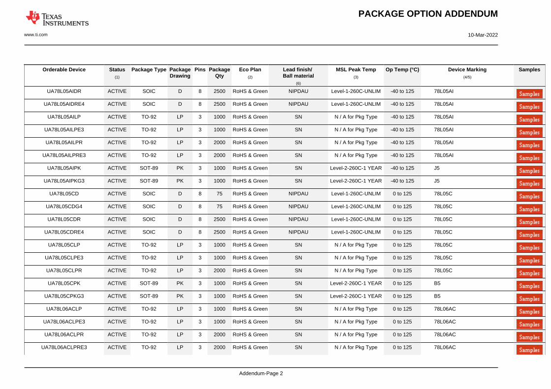
PACKAGE OPTION ADDENDUM
www.ti.com 10-Mar-2022
Addendum-Page 2
Orderable Device Status(1)
Package Type PackageDrawing
Pins PackageQty
Eco Plan(2)
Lead finish/Ball material
(6)
MSL Peak Temp(3)
Op Temp (°C) Device Marking(4/5)
Samples
UA78L05AIDR ACTIVE SOIC D 8 2500 RoHS & Green NIPDAU Level-1-260C-UNLIM -40 to 125 78L05AI
UA78L05AIDRE4 ACTIVE SOIC D 8 2500 RoHS & Green NIPDAU Level-1-260C-UNLIM -40 to 125 78L05AI
UA78L05AILP ACTIVE TO-92 LP 3 1000 RoHS & Green SN N / A for Pkg Type -40 to 125 78L05AI
UA78L05AILPE3 ACTIVE TO-92 LP 3 1000 RoHS & Green SN N / A for Pkg Type -40 to 125 78L05AI
UA78L05AILPR ACTIVE TO-92 LP 3 2000 RoHS & Green SN N / A for Pkg Type -40 to 125 78L05AI
UA78L05AILPRE3 ACTIVE TO-92 LP 3 2000 RoHS & Green SN N / A for Pkg Type -40 to 125 78L05AI
UA78L05AIPK ACTIVE SOT-89 PK 3 1000 RoHS & Green SN Level-2-260C-1 YEAR -40 to 125 J5
UA78L05AIPKG3 ACTIVE SOT-89 PK 3 1000 RoHS & Green SN Level-2-260C-1 YEAR -40 to 125 J5
UA78L05CD ACTIVE SOIC D 8 75 RoHS & Green NIPDAU Level-1-260C-UNLIM 0 to 125 78L05C
UA78L05CDG4 ACTIVE SOIC D 8 75 RoHS & Green NIPDAU Level-1-260C-UNLIM 0 to 125 78L05C
UA78L05CDR ACTIVE SOIC D 8 2500 RoHS & Green NIPDAU Level-1-260C-UNLIM 0 to 125 78L05C
UA78L05CDRE4 ACTIVE SOIC D 8 2500 RoHS & Green NIPDAU Level-1-260C-UNLIM 0 to 125 78L05C
UA78L05CLP ACTIVE TO-92 LP 3 1000 RoHS & Green SN N / A for Pkg Type 0 to 125 78L05C
UA78L05CLPE3 ACTIVE TO-92 LP 3 1000 RoHS & Green SN N / A for Pkg Type 0 to 125 78L05C
UA78L05CLPR ACTIVE TO-92 LP 3 2000 RoHS & Green SN N / A for Pkg Type 0 to 125 78L05C
UA78L05CPK ACTIVE SOT-89 PK 3 1000 RoHS & Green SN Level-2-260C-1 YEAR 0 to 125 B5
UA78L05CPKG3 ACTIVE SOT-89 PK 3 1000 RoHS & Green SN Level-2-260C-1 YEAR 0 to 125 B5
UA78L06ACLP ACTIVE TO-92 LP 3 1000 RoHS & Green SN N / A for Pkg Type 0 to 125 78L06AC
UA78L06ACLPE3 ACTIVE TO-92 LP 3 1000 RoHS & Green SN N / A for Pkg Type 0 to 125 78L06AC
UA78L06ACLPR ACTIVE TO-92 LP 3 2000 RoHS & Green SN N / A for Pkg Type 0 to 125 78L06AC
UA78L06ACLPRE3 ACTIVE TO-92 LP 3 2000 RoHS & Green SN N / A for Pkg Type 0 to 125 78L06AC
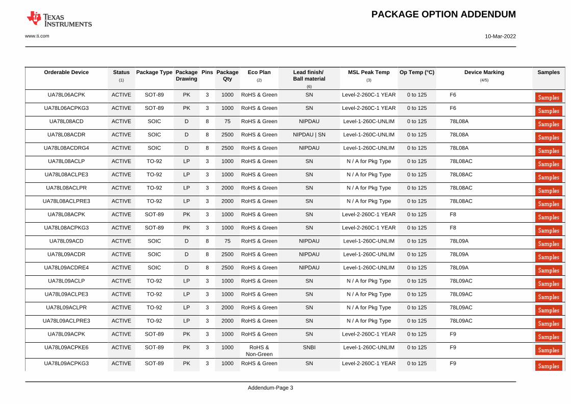
PACKAGE OPTION ADDENDUM
www.ti.com 10-Mar-2022
Addendum-Page 3
Orderable Device Status(1)
Package Type PackageDrawing
Pins PackageQty
Eco Plan(2)
Lead finish/Ball material
(6)
MSL Peak Temp(3)
Op Temp (°C) Device Marking(4/5)
Samples
UA78L06ACPK ACTIVE SOT-89 PK 3 1000 RoHS & Green SN Level-2-260C-1 YEAR 0 to 125 F6
UA78L06ACPKG3 ACTIVE SOT-89 PK 3 1000 RoHS & Green SN Level-2-260C-1 YEAR 0 to 125 F6
UA78L08ACD ACTIVE SOIC D 8 75 RoHS & Green NIPDAU Level-1-260C-UNLIM 0 to 125 78L08A
UA78L08ACDR ACTIVE SOIC D 8 2500 RoHS & Green NIPDAU | SN Level-1-260C-UNLIM 0 to 125 78L08A
UA78L08ACDRG4 ACTIVE SOIC D 8 2500 RoHS & Green NIPDAU Level-1-260C-UNLIM 0 to 125 78L08A
UA78L08ACLP ACTIVE TO-92 LP 3 1000 RoHS & Green SN N / A for Pkg Type 0 to 125 78L08AC
UA78L08ACLPE3 ACTIVE TO-92 LP 3 1000 RoHS & Green SN N / A for Pkg Type 0 to 125 78L08AC
UA78L08ACLPR ACTIVE TO-92 LP 3 2000 RoHS & Green SN N / A for Pkg Type 0 to 125 78L08AC
UA78L08ACLPRE3 ACTIVE TO-92 LP 3 2000 RoHS & Green SN N / A for Pkg Type 0 to 125 78L08AC
UA78L08ACPK ACTIVE SOT-89 PK 3 1000 RoHS & Green SN Level-2-260C-1 YEAR 0 to 125 F8
UA78L08ACPKG3 ACTIVE SOT-89 PK 3 1000 RoHS & Green SN Level-2-260C-1 YEAR 0 to 125 F8
UA78L09ACD ACTIVE SOIC D 8 75 RoHS & Green NIPDAU Level-1-260C-UNLIM 0 to 125 78L09A
UA78L09ACDR ACTIVE SOIC D 8 2500 RoHS & Green NIPDAU Level-1-260C-UNLIM 0 to 125 78L09A
UA78L09ACDRE4 ACTIVE SOIC D 8 2500 RoHS & Green NIPDAU Level-1-260C-UNLIM 0 to 125 78L09A
UA78L09ACLP ACTIVE TO-92 LP 3 1000 RoHS & Green SN N / A for Pkg Type 0 to 125 78L09AC
UA78L09ACLPE3 ACTIVE TO-92 LP 3 1000 RoHS & Green SN N / A for Pkg Type 0 to 125 78L09AC
UA78L09ACLPR ACTIVE TO-92 LP 3 2000 RoHS & Green SN N / A for Pkg Type 0 to 125 78L09AC
UA78L09ACLPRE3 ACTIVE TO-92 LP 3 2000 RoHS & Green SN N / A for Pkg Type 0 to 125 78L09AC
UA78L09ACPK ACTIVE SOT-89 PK 3 1000 RoHS & Green SN Level-2-260C-1 YEAR 0 to 125 F9
UA78L09ACPKE6 ACTIVE SOT-89 PK 3 1000 RoHS &Non-Green
SNBI Level-1-260C-UNLIM 0 to 125 F9
UA78L09ACPKG3 ACTIVE SOT-89 PK 3 1000 RoHS & Green SN Level-2-260C-1 YEAR 0 to 125 F9

PACKAGE OPTION ADDENDUM
www.ti.com 10-Mar-2022
Addendum-Page 4
Orderable Device Status(1)
Package Type PackageDrawing
Pins PackageQty
Eco Plan(2)
Lead finish/Ball material
(6)
MSL Peak Temp(3)
Op Temp (°C) Device Marking(4/5)
Samples
UA78L10ACD ACTIVE SOIC D 8 75 RoHS & Green NIPDAU Level-1-260C-UNLIM 0 to 125 78L10A
UA78L10ACDR ACTIVE SOIC D 8 2500 RoHS & Green NIPDAU Level-1-260C-UNLIM 0 to 125 78L10A
UA78L10ACDRE4 ACTIVE SOIC D 8 2500 RoHS & Green NIPDAU Level-1-260C-UNLIM 0 to 125 78L10A
UA78L10ACLP ACTIVE TO-92 LP 3 1000 RoHS & Green SN N / A for Pkg Type 0 to 125 78L10AC
UA78L10ACLPE3 ACTIVE TO-92 LP 3 1000 RoHS & Green SN N / A for Pkg Type 0 to 125 78L10AC
UA78L10ACLPR ACTIVE TO-92 LP 3 2000 RoHS & Green SN N / A for Pkg Type 0 to 125 78L10AC
UA78L10ACLPRE3 ACTIVE TO-92 LP 3 2000 RoHS & Green SN N / A for Pkg Type 0 to 125 78L10AC
UA78L10ACPK ACTIVE SOT-89 PK 3 1000 RoHS & Green SN Level-2-260C-1 YEAR 0 to 125 FA
UA78L10ACPKG3 ACTIVE SOT-89 PK 3 1000 RoHS & Green SN Level-2-260C-1 YEAR 0 to 125 FA
UA78L12ACD ACTIVE SOIC D 8 75 RoHS & Green NIPDAU Level-1-260C-UNLIM 0 to 125 78L12A
UA78L12ACDG4 ACTIVE SOIC D 8 75 RoHS & Green NIPDAU Level-1-260C-UNLIM 0 to 125 78L12A
UA78L12ACDR ACTIVE SOIC D 8 2500 RoHS & Green NIPDAU | SN Level-1-260C-UNLIM 0 to 125 78L12A
UA78L12ACDRE4 ACTIVE SOIC D 8 2500 RoHS & Green NIPDAU Level-1-260C-UNLIM 0 to 125 78L12A
UA78L12ACDRG4 ACTIVE SOIC D 8 2500 RoHS & Green NIPDAU Level-1-260C-UNLIM 0 to 125 78L12A
UA78L12ACLP ACTIVE TO-92 LP 3 1000 RoHS & Green SN N / A for Pkg Type 0 to 125 78L12AC
UA78L12ACLPE3 ACTIVE TO-92 LP 3 1000 RoHS & Green SN N / A for Pkg Type 0 to 125 78L12AC
UA78L12ACLPM ACTIVE TO-92 LP 3 2000 RoHS & Green SN N / A for Pkg Type 0 to 125 78L12AC
UA78L12ACLPR ACTIVE TO-92 LP 3 2000 RoHS & Green SN N / A for Pkg Type 0 to 125 78L12AC
UA78L12ACPK ACTIVE SOT-89 PK 3 1000 RoHS & Green SN Level-2-260C-1 YEAR 0 to 125 FC
UA78L12ACPKG3 ACTIVE SOT-89 PK 3 1000 RoHS & Green SN Level-2-260C-1 YEAR 0 to 125 FC
UA78L15ACD ACTIVE SOIC D 8 75 RoHS & Green NIPDAU Level-1-260C-UNLIM 0 to 125 78L15A

PACKAGE OPTION ADDENDUM
www.ti.com 10-Mar-2022
Addendum-Page 5
Orderable Device Status(1)
Package Type PackageDrawing
Pins PackageQty
Eco Plan(2)
Lead finish/Ball material
(6)
MSL Peak Temp(3)
Op Temp (°C) Device Marking(4/5)
Samples
UA78L15ACDR ACTIVE SOIC D 8 2500 RoHS & Green NIPDAU Level-1-260C-UNLIM 0 to 125 78L15A
UA78L15ACDRE4 ACTIVE SOIC D 8 2500 RoHS & Green NIPDAU Level-1-260C-UNLIM 0 to 125 78L15A
UA78L15ACLP ACTIVE TO-92 LP 3 1000 RoHS & Green SN N / A for Pkg Type 0 to 125 78L15AC
UA78L15ACLPE3 ACTIVE TO-92 LP 3 1000 RoHS & Green SN N / A for Pkg Type 0 to 125 78L15AC
UA78L15ACLPR ACTIVE TO-92 LP 3 2000 RoHS & Green SN N / A for Pkg Type 0 to 125 78L15AC
UA78L15ACLPRE3 ACTIVE TO-92 LP 3 2000 RoHS & Green SN N / A for Pkg Type 0 to 125 78L15AC
UA78L15ACPK ACTIVE SOT-89 PK 3 1000 RoHS & Green SN Level-2-260C-1 YEAR 0 to 125 FF
UA78L15ACPKG3 ACTIVE SOT-89 PK 3 1000 RoHS & Green SN Level-2-260C-1 YEAR 0 to 125 FF
(1) The marketing status values are defined as follows:ACTIVE: Product device recommended for new designs.LIFEBUY: TI has announced that the device will be discontinued, and a lifetime-buy period is in effect.NRND: Not recommended for new designs. Device is in production to support existing customers, but TI does not recommend using this part in a new design.PREVIEW: Device has been announced but is not in production. Samples may or may not be available.OBSOLETE: TI has discontinued the production of the device.
(2) RoHS: TI defines "RoHS" to mean semiconductor products that are compliant with the current EU RoHS requirements for all 10 RoHS substances, including the requirement that RoHS substancedo not exceed 0.1% by weight in homogeneous materials. Where designed to be soldered at high temperatures, "RoHS" products are suitable for use in specified lead-free processes. TI mayreference these types of products as "Pb-Free".RoHS Exempt: TI defines "RoHS Exempt" to mean products that contain lead but are compliant with EU RoHS pursuant to a specific EU RoHS exemption.Green: TI defines "Green" to mean the content of Chlorine (Cl) and Bromine (Br) based flame retardants meet JS709B low halogen requirements of <=1000ppm threshold. Antimony trioxide basedflame retardants must also meet the <=1000ppm threshold requirement.
(3) MSL, Peak Temp. - The Moisture Sensitivity Level rating according to the JEDEC industry standard classifications, and peak solder temperature.
(4) There may be additional marking, which relates to the logo, the lot trace code information, or the environmental category on the device.
(5) Multiple Device Markings will be inside parentheses. Only one Device Marking contained in parentheses and separated by a "~" will appear on a device. If a line is indented then it is a continuationof the previous line and the two combined represent the entire Device Marking for that device.

PACKAGE OPTION ADDENDUM
www.ti.com 10-Mar-2022
Addendum-Page 6
(6) Lead finish/Ball material - Orderable Devices may have multiple material finish options. Finish options are separated by a vertical ruled line. Lead finish/Ball material values may wrap to twolines if the finish value exceeds the maximum column width.
Important Information and Disclaimer:The information provided on this page represents TI's knowledge and belief as of the date that it is provided. TI bases its knowledge and belief on informationprovided by third parties, and makes no representation or warranty as to the accuracy of such information. Efforts are underway to better integrate information from third parties. TI has taken andcontinues to take reasonable steps to provide representative and accurate information but may not have conducted destructive testing or chemical analysis on incoming materials and chemicals.TI and TI suppliers consider certain information to be proprietary, and thus CAS numbers and other limited information may not be available for release.
In no event shall TI's liability arising out of such information exceed the total purchase price of the TI part(s) at issue in this document sold by TI to Customer on an annual basis.
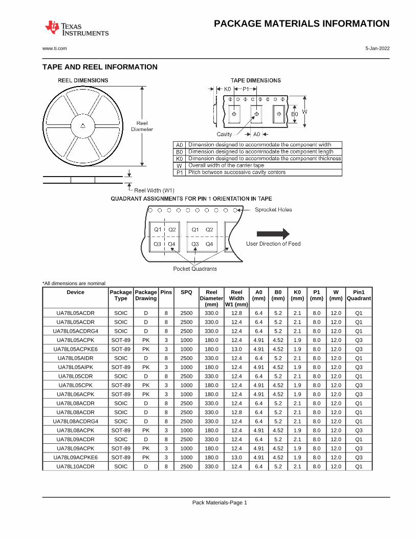
TAPE AND REEL INFORMATION
*All dimensions are nominal
Device PackageType
PackageDrawing
Pins SPQ ReelDiameter
(mm)
ReelWidth
W1 (mm)
A0(mm)
B0(mm)
K0(mm)
P1(mm)
W(mm)
Pin1Quadrant
UA78L05ACDR SOIC D 8 2500 330.0 12.8 6.4 5.2 2.1 8.0 12.0 Q1
UA78L05ACDR SOIC D 8 2500 330.0 12.4 6.4 5.2 2.1 8.0 12.0 Q1
UA78L05ACDRG4 SOIC D 8 2500 330.0 12.4 6.4 5.2 2.1 8.0 12.0 Q1
UA78L05ACPK SOT-89 PK 3 1000 180.0 12.4 4.91 4.52 1.9 8.0 12.0 Q3
UA78L05ACPKE6 SOT-89 PK 3 1000 180.0 13.0 4.91 4.52 1.9 8.0 12.0 Q3
UA78L05AIDR SOIC D 8 2500 330.0 12.4 6.4 5.2 2.1 8.0 12.0 Q1
UA78L05AIPK SOT-89 PK 3 1000 180.0 12.4 4.91 4.52 1.9 8.0 12.0 Q3
UA78L05CDR SOIC D 8 2500 330.0 12.4 6.4 5.2 2.1 8.0 12.0 Q1
UA78L05CPK SOT-89 PK 3 1000 180.0 12.4 4.91 4.52 1.9 8.0 12.0 Q3
UA78L06ACPK SOT-89 PK 3 1000 180.0 12.4 4.91 4.52 1.9 8.0 12.0 Q3
UA78L08ACDR SOIC D 8 2500 330.0 12.4 6.4 5.2 2.1 8.0 12.0 Q1
UA78L08ACDR SOIC D 8 2500 330.0 12.8 6.4 5.2 2.1 8.0 12.0 Q1
UA78L08ACDRG4 SOIC D 8 2500 330.0 12.4 6.4 5.2 2.1 8.0 12.0 Q1
UA78L08ACPK SOT-89 PK 3 1000 180.0 12.4 4.91 4.52 1.9 8.0 12.0 Q3
UA78L09ACDR SOIC D 8 2500 330.0 12.4 6.4 5.2 2.1 8.0 12.0 Q1
UA78L09ACPK SOT-89 PK 3 1000 180.0 12.4 4.91 4.52 1.9 8.0 12.0 Q3
UA78L09ACPKE6 SOT-89 PK 3 1000 180.0 13.0 4.91 4.52 1.9 8.0 12.0 Q3
UA78L10ACDR SOIC D 8 2500 330.0 12.4 6.4 5.2 2.1 8.0 12.0 Q1
PACKAGE MATERIALS INFORMATION
www.ti.com 5-Jan-2022
Pack Materials-Page 1
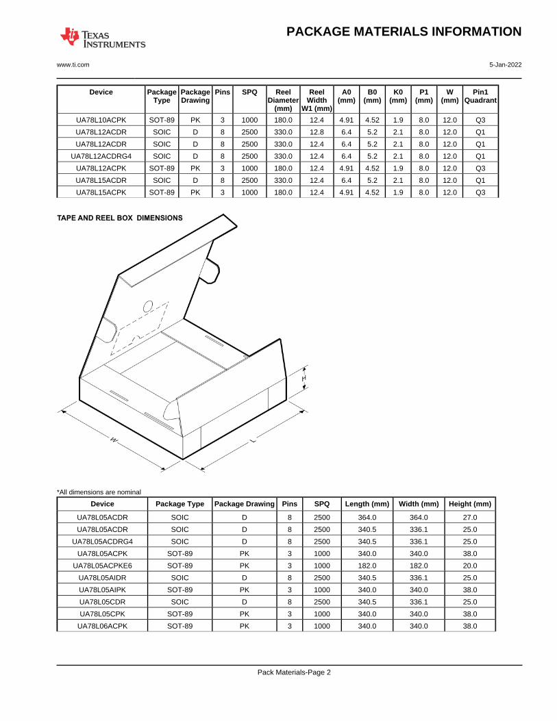
Device PackageType
PackageDrawing
Pins SPQ ReelDiameter
(mm)
ReelWidth
W1 (mm)
A0(mm)
B0(mm)
K0(mm)
P1(mm)
W(mm)
Pin1Quadrant
UA78L10ACPK SOT-89 PK 3 1000 180.0 12.4 4.91 4.52 1.9 8.0 12.0 Q3
UA78L12ACDR SOIC D 8 2500 330.0 12.8 6.4 5.2 2.1 8.0 12.0 Q1
UA78L12ACDR SOIC D 8 2500 330.0 12.4 6.4 5.2 2.1 8.0 12.0 Q1
UA78L12ACDRG4 SOIC D 8 2500 330.0 12.4 6.4 5.2 2.1 8.0 12.0 Q1
UA78L12ACPK SOT-89 PK 3 1000 180.0 12.4 4.91 4.52 1.9 8.0 12.0 Q3
UA78L15ACDR SOIC D 8 2500 330.0 12.4 6.4 5.2 2.1 8.0 12.0 Q1
UA78L15ACPK SOT-89 PK 3 1000 180.0 12.4 4.91 4.52 1.9 8.0 12.0 Q3
*All dimensions are nominal
Device Package Type Package Drawing Pins SPQ Length (mm) Width (mm) Height (mm)
UA78L05ACDR SOIC D 8 2500 364.0 364.0 27.0
UA78L05ACDR SOIC D 8 2500 340.5 336.1 25.0
UA78L05ACDRG4 SOIC D 8 2500 340.5 336.1 25.0
UA78L05ACPK SOT-89 PK 3 1000 340.0 340.0 38.0
UA78L05ACPKE6 SOT-89 PK 3 1000 182.0 182.0 20.0
UA78L05AIDR SOIC D 8 2500 340.5 336.1 25.0
UA78L05AIPK SOT-89 PK 3 1000 340.0 340.0 38.0
UA78L05CDR SOIC D 8 2500 340.5 336.1 25.0
UA78L05CPK SOT-89 PK 3 1000 340.0 340.0 38.0
UA78L06ACPK SOT-89 PK 3 1000 340.0 340.0 38.0
PACKAGE MATERIALS INFORMATION
www.ti.com 5-Jan-2022
Pack Materials-Page 2
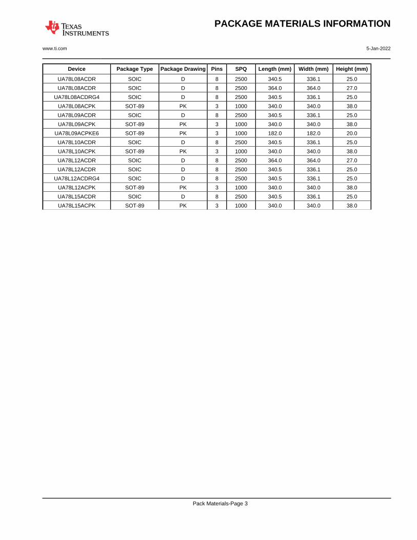
Device Package Type Package Drawing Pins SPQ Length (mm) Width (mm) Height (mm)
UA78L08ACDR SOIC D 8 2500 340.5 336.1 25.0
UA78L08ACDR SOIC D 8 2500 364.0 364.0 27.0
UA78L08ACDRG4 SOIC D 8 2500 340.5 336.1 25.0
UA78L08ACPK SOT-89 PK 3 1000 340.0 340.0 38.0
UA78L09ACDR SOIC D 8 2500 340.5 336.1 25.0
UA78L09ACPK SOT-89 PK 3 1000 340.0 340.0 38.0
UA78L09ACPKE6 SOT-89 PK 3 1000 182.0 182.0 20.0
UA78L10ACDR SOIC D 8 2500 340.5 336.1 25.0
UA78L10ACPK SOT-89 PK 3 1000 340.0 340.0 38.0
UA78L12ACDR SOIC D 8 2500 364.0 364.0 27.0
UA78L12ACDR SOIC D 8 2500 340.5 336.1 25.0
UA78L12ACDRG4 SOIC D 8 2500 340.5 336.1 25.0
UA78L12ACPK SOT-89 PK 3 1000 340.0 340.0 38.0
UA78L15ACDR SOIC D 8 2500 340.5 336.1 25.0
UA78L15ACPK SOT-89 PK 3 1000 340.0 340.0 38.0
PACKAGE MATERIALS INFORMATION
www.ti.com 5-Jan-2022
Pack Materials-Page 3

TUBE
*All dimensions are nominal
Device Package Name Package Type Pins SPQ L (mm) W (mm) T (µm) B (mm)
UA78L02ACD D SOIC 8 75 507 8 3940 4.32
UA78L02ACDG4 D SOIC 8 75 507 8 3940 4.32
UA78L05ACD D SOIC 8 75 507 8 3940 4.32
UA78L05ACDE4 D SOIC 8 75 507 8 3940 4.32
UA78L05ACDG4 D SOIC 8 75 507 8 3940 4.32
UA78L05AID D SOIC 8 75 507 8 3940 4.32
UA78L05CD D SOIC 8 75 507 8 3940 4.32
UA78L05CDG4 D SOIC 8 75 507 8 3940 4.32
UA78L08ACD D SOIC 8 75 507 8 3940 4.32
UA78L09ACD D SOIC 8 75 507 8 3940 4.32
UA78L10ACD D SOIC 8 75 507 8 3940 4.32
UA78L12ACD D SOIC 8 75 507 8 3940 4.32
UA78L12ACDG4 D SOIC 8 75 507 8 3940 4.32
UA78L15ACD D SOIC 8 75 507 8 3940 4.32
PACKAGE MATERIALS INFORMATION
www.ti.com 5-Jan-2022
Pack Materials-Page 4


www.ti.com
PACKAGE OUTLINE
C
.228-.244 TYP[5.80-6.19]
.069 MAX[1.75]
6X .050[1.27]
8X .012-.020 [0.31-0.51]
2X.150[3.81]
.005-.010 TYP[0.13-0.25]
0 - 8 .004-.010[0.11-0.25]
.010[0.25]
.016-.050[0.41-1.27]
4X (0 -15 )
A
.189-.197[4.81-5.00]
NOTE 3
B .150-.157[3.81-3.98]
NOTE 4
4X (0 -15 )
(.041)[1.04]
SOIC - 1.75 mm max heightD0008ASMALL OUTLINE INTEGRATED CIRCUIT
4214825/C 02/2019
NOTES: 1. Linear dimensions are in inches [millimeters]. Dimensions in parenthesis are for reference only. Controlling dimensions are in inches. Dimensioning and tolerancing per ASME Y14.5M. 2. This drawing is subject to change without notice. 3. This dimension does not include mold flash, protrusions, or gate burrs. Mold flash, protrusions, or gate burrs shall not exceed .006 [0.15] per side. 4. This dimension does not include interlead flash.5. Reference JEDEC registration MS-012, variation AA.
18
.010 [0.25] C A B
54
PIN 1 ID AREA
SEATING PLANE
.004 [0.1] C
SEE DETAIL A
DETAIL ATYPICAL
SCALE 2.800
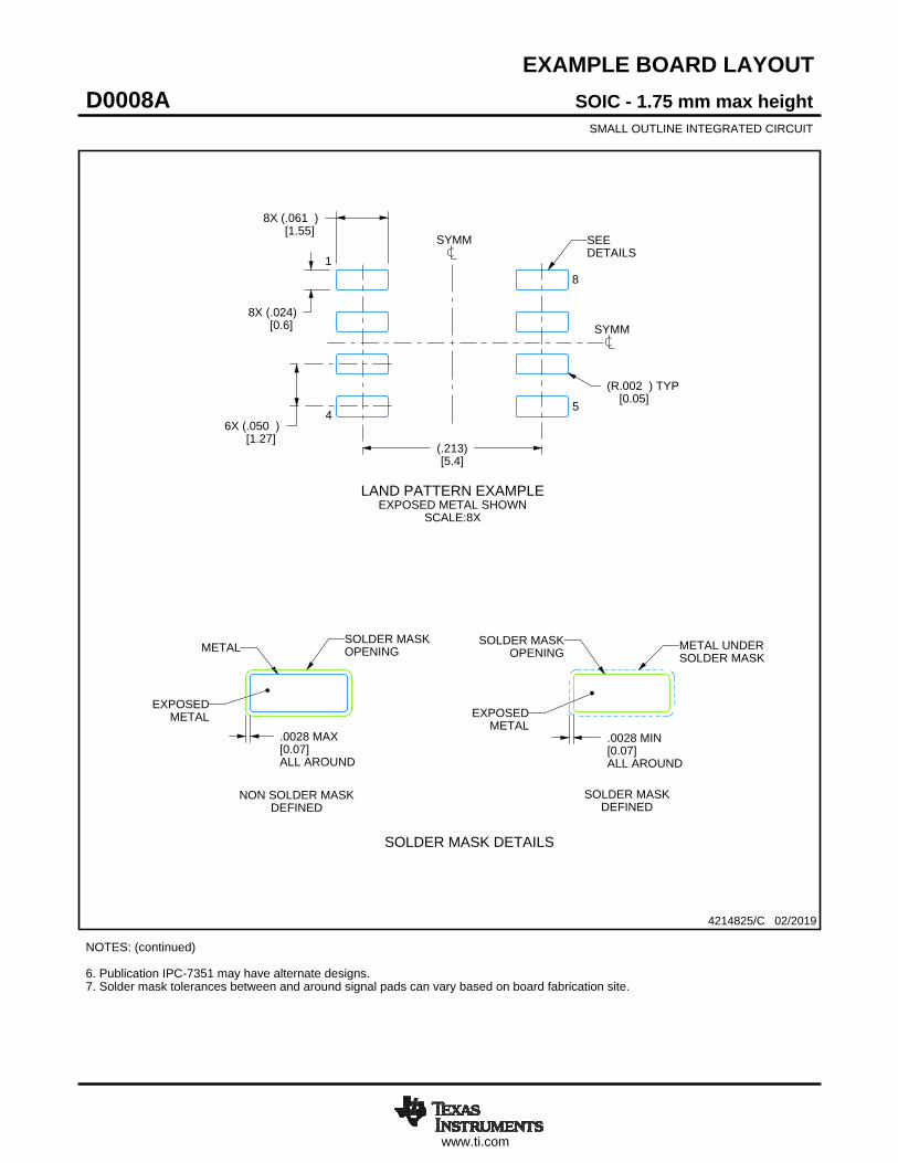
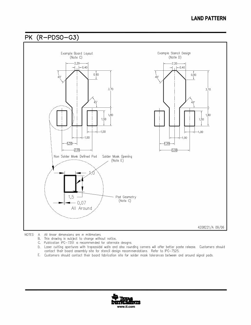
www.ti.com
EXAMPLE BOARD LAYOUT
.0028 MAX[0.07]ALL AROUND
.0028 MIN[0.07]ALL AROUND
(.213)[5.4]
6X (.050 )[1.27]
8X (.061 )[1.55]
8X (.024)[0.6]
(R.002 ) TYP[0.05]
SOIC - 1.75 mm max heightD0008ASMALL OUTLINE INTEGRATED CIRCUIT
4214825/C 02/2019
NOTES: (continued) 6. Publication IPC-7351 may have alternate designs. 7. Solder mask tolerances between and around signal pads can vary based on board fabrication site.
METALSOLDER MASKOPENING
NON SOLDER MASKDEFINED
SOLDER MASK DETAILS
EXPOSEDMETAL
OPENINGSOLDER MASK METAL UNDER
SOLDER MASK
SOLDER MASKDEFINED
EXPOSEDMETAL
LAND PATTERN EXAMPLEEXPOSED METAL SHOWN
SCALE:8X
SYMM
1
45
8
SEEDETAILS
SYMM

www.ti.com
EXAMPLE STENCIL DESIGN
8X (.061 )[1.55]
8X (.024)[0.6]
6X (.050 )[1.27]
(.213)[5.4]
(R.002 ) TYP[0.05]
SOIC - 1.75 mm max heightD0008ASMALL OUTLINE INTEGRATED CIRCUIT
4214825/C 02/2019
NOTES: (continued) 8. Laser cutting apertures with trapezoidal walls and rounded corners may offer better paste release. IPC-7525 may have alternate design recommendations. 9. Board assembly site may have different recommendations for stencil design.
SOLDER PASTE EXAMPLEBASED ON .005 INCH [0.125 MM] THICK STENCIL
SCALE:8X
SYMM
SYMM
1
45
8
www.ti.com
PACKAGE OUTLINE
3X 2.672.03
5.214.44
5.344.32
3X12.7 MIN
2X 1.27 0.13
3X 0.550.38
4.193.17
3.43 MIN
3X 0.430.35
(2.54)NOTE 3
2X2.6 0.2
2X4 MAX
SEATINGPLANE
6X0.076 MAX
(0.51) TYP
(1.5) TYP
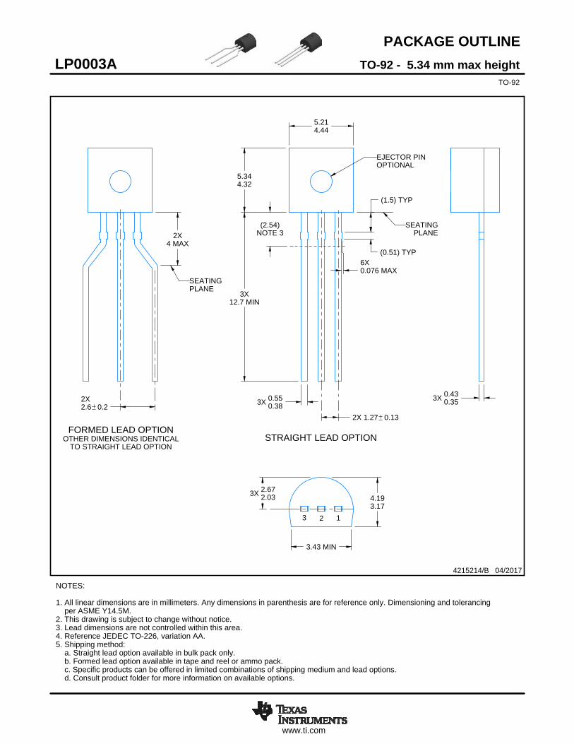
TO-92 - 5.34 mm max heightLP0003ATO-92
4215214/B 04/2017
NOTES: 1. All linear dimensions are in millimeters. Any dimensions in parenthesis are for reference only. Dimensioning and tolerancing per ASME Y14.5M.2. This drawing is subject to change without notice.3. Lead dimensions are not controlled within this area.4. Reference JEDEC TO-226, variation AA.5. Shipping method: a. Straight lead option available in bulk pack only. b. Formed lead option available in tape and reel or ammo pack. c. Specific products can be offered in limited combinations of shipping medium and lead options. d. Consult product folder for more information on available options.
EJECTOR PINOPTIONAL
PLANESEATING
STRAIGHT LEAD OPTION
3 2 1
SCALE 1.200
FORMED LEAD OPTIONOTHER DIMENSIONS IDENTICAL
TO STRAIGHT LEAD OPTION
SCALE 1.200
www.ti.com
EXAMPLE BOARD LAYOUT
0.05 MAXALL AROUND
TYP
(1.07)
(1.5) 2X (1.5)
2X (1.07)(1.27)
(2.54)
FULL RTYP
( 1.4)0.05 MAXALL AROUND
TYP
(2.6)
(5.2)
(R0.05) TYP
3X ( 0.9) HOLE
2X ( 1.4)METAL
3X ( 0.85) HOLE
(R0.05) TYP
4215214/B 04/2017
TO-92 - 5.34 mm max heightLP0003ATO-92
LAND PATTERN EXAMPLEFORMED LEAD OPTIONNON-SOLDER MASK DEFINED
SCALE:15X
SOLDER MASKOPENING
METAL
2XSOLDER MASKOPENING
1 2 3
LAND PATTERN EXAMPLESTRAIGHT LEAD OPTIONNON-SOLDER MASK DEFINED
SCALE:15X
METALTYP
SOLDER MASKOPENING
2XSOLDER MASKOPENING
2XMETAL
1 2 3
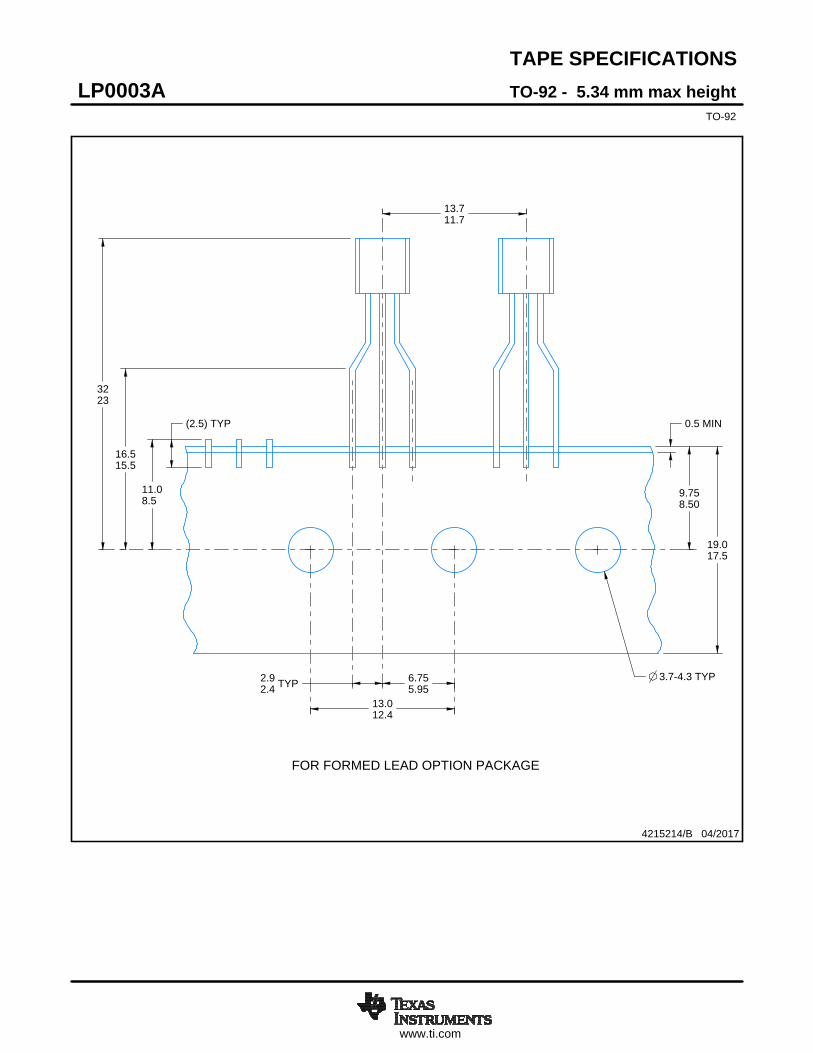
www.ti.com
TAPE SPECIFICATIONS
19.017.5
13.711.7
11.08.5
0.5 MIN
TYP-4.33.7
9.758.50
TYP2.92.4
6.755.95
13.012.4
(2.5) TYP
16.515.5
3223
4215214/B 04/2017
TO-92 - 5.34 mm max heightLP0003ATO-92
FOR FORMED LEAD OPTION PACKAGE

IMPORTANT NOTICE AND DISCLAIMERTI PROVIDES TECHNICAL AND RELIABILITY DATA (INCLUDING DATA SHEETS), DESIGN RESOURCES (INCLUDING REFERENCE DESIGNS), APPLICATION OR OTHER DESIGN ADVICE, WEB TOOLS, SAFETY INFORMATION, AND OTHER RESOURCES “AS IS” AND WITH ALL FAULTS, AND DISCLAIMS ALL WARRANTIES, EXPRESS AND IMPLIED, INCLUDING WITHOUT LIMITATION ANY IMPLIED WARRANTIES OF MERCHANTABILITY, FITNESS FOR A PARTICULAR PURPOSE OR NON-INFRINGEMENT OF THIRD PARTY INTELLECTUAL PROPERTY RIGHTS.These resources are intended for skilled developers designing with TI products. You are solely responsible for (1) selecting the appropriate TI products for your application, (2) designing, validating and testing your application, and (3) ensuring your application meets applicable standards, and any other safety, security, regulatory or other requirements.These resources are subject to change without notice. TI grants you permission to use these resources only for development of an application that uses the TI products described in the resource. Other reproduction and display of these resources is prohibited. No license is granted to any other TI intellectual property right or to any third party intellectual property right. TI disclaims responsibility for, and you will fully indemnify TI and its representatives against, any claims, damages, costs, losses, and liabilities arising out of your use of these resources.TI’s products are provided subject to TI’s Terms of Sale or other applicable terms available either on ti.com or provided in conjunction with such TI products. TI’s provision of these resources does not expand or otherwise alter TI’s applicable warranties or warranty disclaimers for TI products.TI objects to and rejects any additional or different terms you may have proposed. IMPORTANT NOTICE
Mailing Address: Texas Instruments, Post Office Box 655303, Dallas, Texas 75265Copyright © 2022, Texas Instruments Incorporated