twr-kv11z75m tower system module user's...
TRANSCRIPT
© 2015 Freescale Semiconductor, Inc. All rights reserved.
TWR-KV11Z75M Tower System Module
User’s Guide
1. Overview
The TWR-KV11Z75M Tower System Module is the
entry level member of the Kinetis-based Microcontroller
family specifically labeled “Kinetis V-Series”. On a
single chip, it combines the processing power of up to 75
MHz ARM® Cortex®-M0+ CPU with up to 128 KB flash,
16 KB RAM, a motor control timer, and an ADC with
capability to capture two inputs simultaneously (two
current phase measurements), within a period of 800
nanosiemens (nS) to 1 microsiemens (uS). It has a full set
of programmable peripherals, including two 6 channel
PWM timers to drive two 3-phase complimentary inverter
stages, four 2 channel PWM timers, 2x 16 bit ADCs with
two capture and hold circuits and 1 uS conversion speed,
two UART, one SPI, I2C, CRC block, Analog
Comparators with DAC, CAN and on-chip/off-chip clock
sources, and a 12b DAC. Each peripheral can be
independently shut down to save power. It can work with
a power supply voltage range from 1.71 V to 3.6 V.
The KV11 board is targeted for low dynamic variable
speed with dual BLDC 6-step sensorless motor control
used in industrial pumps, compressors, fans, and power
conversion, as well as other general purpose applications.
The Tower board is designed to easily evaluate these
modules and help customers build the prototype for
development.
The TWR-KV11Z75M Tower System module has a 64-
LQFP chip soldered directly on the PCB. The module
works with temperatures ranging between -40゜C to
105゜C.
Freescale Semiconductor, Inc. Document Number: TWRKV11Z75MUG
User’s Guide Rev. 0 , 06/2015
Contents
1. Overview 1 2. Get to know the TWR-KV11Z75M Tower System
module 3 3. Hardware description 4
3.1. Block diagram ......................................................... 4 3.2. Microcontroller ....................................................... 4 3.3. Clocking .................................................................. 5 3.4. System power .......................................................... 5 3.5. Debug interface ....................................................... 6 3.6. Accelerometer ......................................................... 8 3.7. User interfaces ........................................................ 9 3.8. Interface connectors .............................................. 12
4. TWR-KV11Z75M Options and headers 14 5. References 16 6. Useful links 16 7. Revision History 16
Overview
TWR-KV11Z75M Tower System Module User’s Guide, User’s Guide, Rev. 0, 06/2015
2 Freescale Semiconductor, Inc.
The following list summarizes the features of the TWR-KV11Z75M Tower System module:
64-LQFP KV11 Microcontroller.
High-speed CAN transceiver TJA1051T/3.
On-board OpenSDA with USB connection used to debug code without an external debug
interface.
Header for standard min Cortex SWD connector used to debug code on either OpenSDA or
KV11 with external debug interface.
Power indication LED.
10 MHz crystal on board for the microcontroller.
FX0S87000CQ 3-axis digital accelerometer and magnetometer.
Eight LEDs connected with buffers to PWM channels for dimming.
Two push buttons for user input or interrupts to the microcontroller.
Four thermistors for single-ended or differential analog inputs.
Reset push button for KV11.
Elevator signal supporting TWR-MCLV3PH.
Header to connect to APMOTOR56F800E motor board.
Can be powered by an external supply such as the APMOTOR56F800E motor board and TWR-
MCLV3PH.
Headers to connect SCI0 and SCI1 signals to either OpenSDA or an elevator board.
2-pin jumper for current measurement.
Get to know the TWR-KV11Z75M Tower System module
TWR-KV11Z75M Tower System Module User’s Guide, User’s Guide, Rev. 0, 06/2015
Freescale Semiconductor, Inc. 3
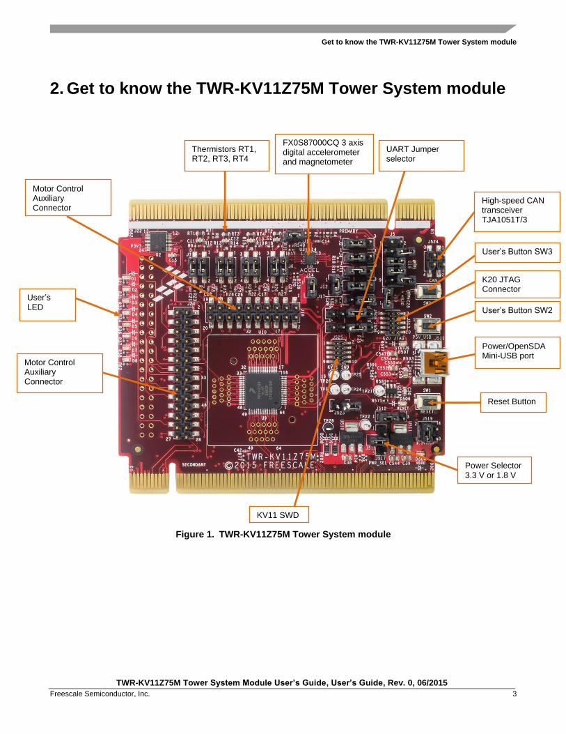
2. Get to know the TWR-KV11Z75M Tower System module
Figure 1. TWR-KV11Z75M Tower System module
Thermistors RT1, RT2, RT3, RT4
FX0S87000CQ 3 axis digital accelerometer and magnetometer
User’s LED
High-speed CAN transceiver TJA1051T/3
KV11 SWD Connector
User’s Button SW3
User’s Button SW2
Reset Button
Power/OpenSDA Mini-USB port
Motor Control Auxiliary Connector
Motor Control Auxiliary Connector
Power Selector 3.3 V or 1.8 V
K20 JTAG Connector
UART Jumper selector
Hardware description
TWR-KV11Z75M Tower System Module User’s Guide, User’s Guide, Rev. 0, 06/2015
4 Freescale Semiconductor, Inc.
3. Hardware description
This section provides specification details for the TWR-KV11Z75M Tower System module.
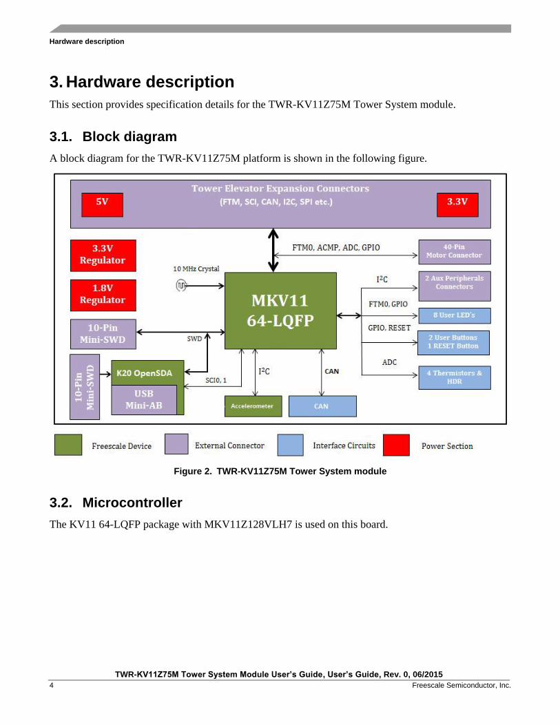
3.1. Block diagram
A block diagram for the TWR-KV11Z75M platform is shown in the following figure.
Figure 2. TWR-KV11Z75M Tower System module
3.2. Microcontroller
The KV11 64-LQFP package with MKV11Z128VLH7 is used on this board.
Hardware description
TWR-KV11Z75M Tower System Module User’s Guide, User’s Guide, Rev. 0, 06/2015
Freescale Semiconductor, Inc. 5
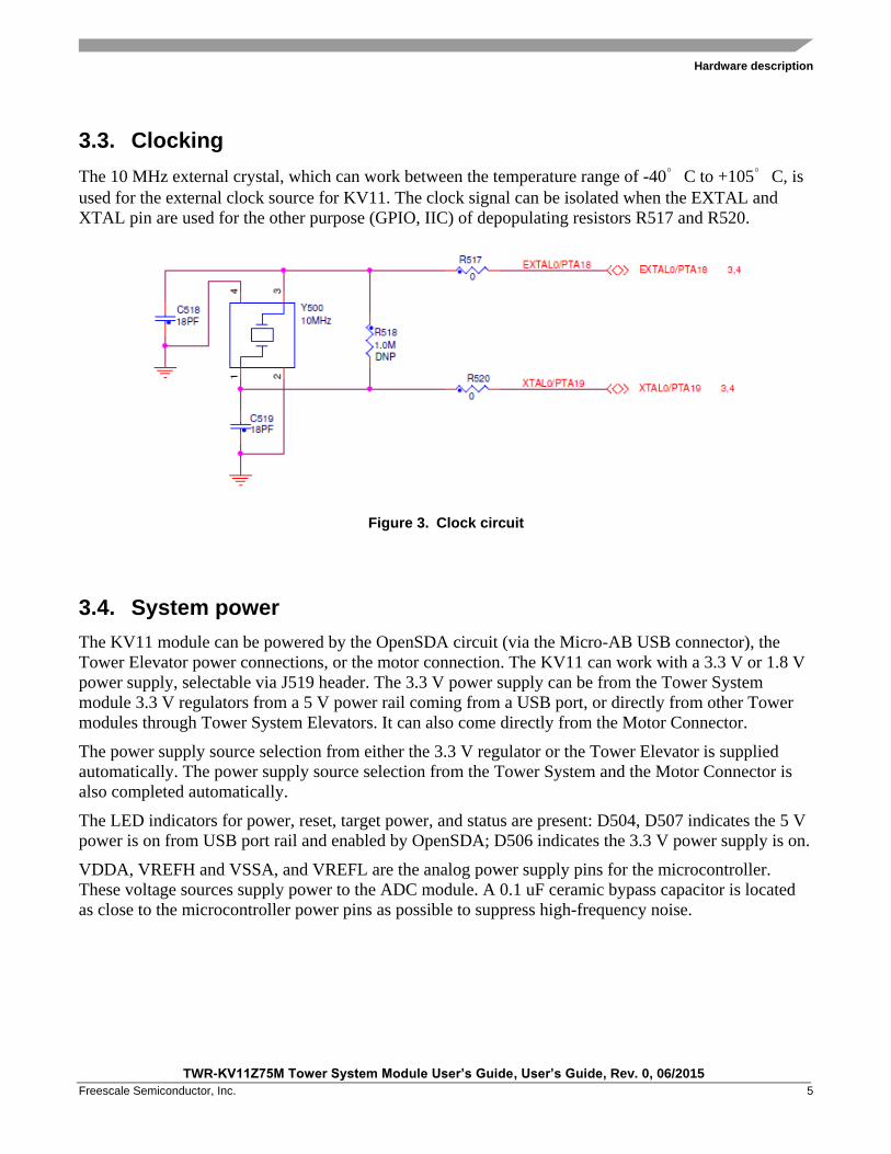
3.3. Clocking
The 10 MHz external crystal, which can work between the temperature range of -40゜C to +105゜C, is
used for the external clock source for KV11. The clock signal can be isolated when the EXTAL and
XTAL pin are used for the other purpose (GPIO, IIC) of depopulating resistors R517 and R520.
Figure 3. Clock circuit
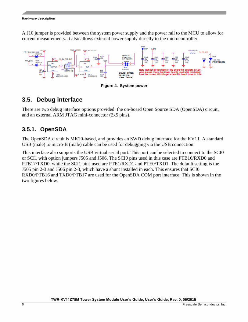
3.4. System power
The KV11 module can be powered by the OpenSDA circuit (via the Micro-AB USB connector), the
Tower Elevator power connections, or the motor connection. The KV11 can work with a 3.3 V or 1.8 V
power supply, selectable via J519 header. The 3.3 V power supply can be from the Tower System
module 3.3 V regulators from a 5 V power rail coming from a USB port, or directly from other Tower
modules through Tower System Elevators. It can also come directly from the Motor Connector.
The power supply source selection from either the 3.3 V regulator or the Tower Elevator is supplied
automatically. The power supply source selection from the Tower System and the Motor Connector is
also completed automatically.
The LED indicators for power, reset, target power, and status are present: D504, D507 indicates the 5 V
power is on from USB port rail and enabled by OpenSDA; D506 indicates the 3.3 V power supply is on.
VDDA, VREFH and VSSA, and VREFL are the analog power supply pins for the microcontroller.
These voltage sources supply power to the ADC module. A 0.1 uF ceramic bypass capacitor is located
as close to the microcontroller power pins as possible to suppress high-frequency noise.
Hardware description
TWR-KV11Z75M Tower System Module User’s Guide, User’s Guide, Rev. 0, 06/2015
6 Freescale Semiconductor, Inc.
A J10 jumper is provided between the system power supply and the power rail to the MCU to allow for
current measurements. It also allows external power supply directly to the microcontroller.
Figure 4. System power
3.5. Debug interface
There are two debug interface options provided: the on-board Open Source SDA (OpenSDA) circuit,
and an external ARM JTAG mini-connector (2x5 pins).
3.5.1. OpenSDA
The OpenSDA circuit is MK20-based, and provides an SWD debug interface for the KV11. A standard
USB (male) to micro-B (male) cable can be used for debugging via the USB connection.
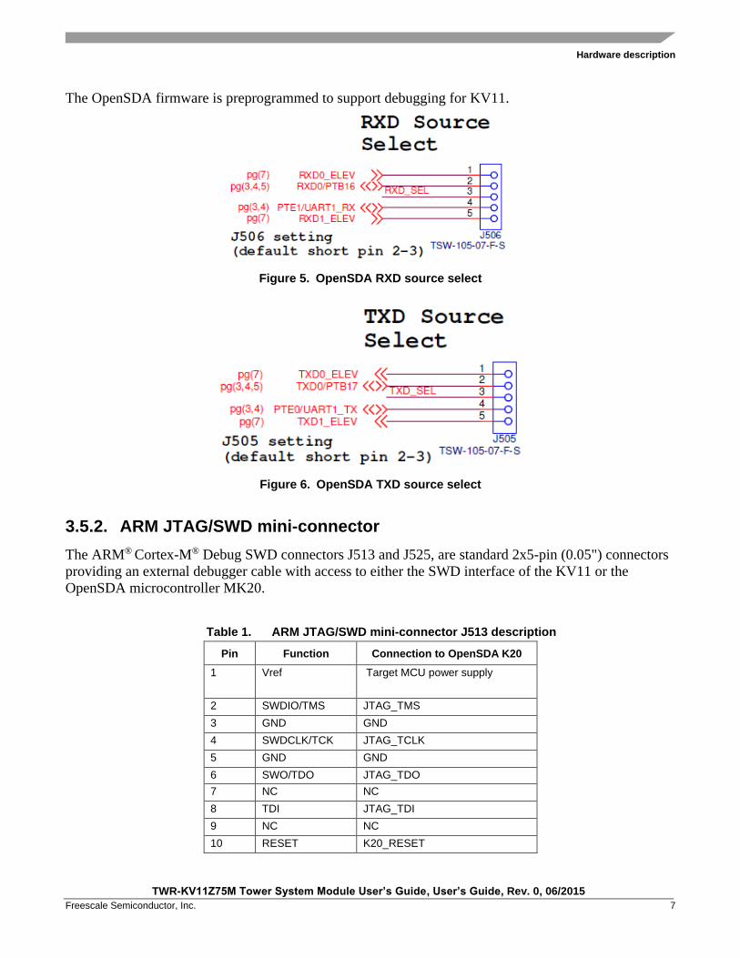
This interface also supports the USB virtual serial port. This port can be selected to connect to the SCI0
or SCI1 with option jumpers J505 and J506. The SCI0 pins used in this case are PTB16/RXD0 and
PTB17/TXD0, while the SCI1 pins used are PTE1/RXD1 and PTE0/TXD1. The default setting is the
J505 pin 2-3 and J506 pin 2-3, which have a shunt installed in each. This ensures that SCI0
RXD0/PTB16 and TXD0/PTB17 are used for the OpenSDA COM port interface. This is shown in the
two figures below.
Hardware description
TWR-KV11Z75M Tower System Module User’s Guide, User’s Guide, Rev. 0, 06/2015
Freescale Semiconductor, Inc. 7
The OpenSDA firmware is preprogrammed to support debugging for KV11.
Figure 5. OpenSDA RXD source select
Figure 6. OpenSDA TXD source select
3.5.2. ARM JTAG/SWD mini-connector
The ARM® Cortex-M® Debug SWD connectors J513 and J525, are standard 2x5-pin (0.05") connectors
providing an external debugger cable with access to either the SWD interface of the KV11 or the
OpenSDA microcontroller MK20.
Table 1. ARM JTAG/SWD mini-connector J513 description
Pin Function Connection to OpenSDA K20
1 Vref Target MCU power supply
2 SWDIO/TMS JTAG_TMS
3 GND GND
4 SWDCLK/TCK JTAG_TCLK
5 GND GND
6 SWO/TDO JTAG_TDO
7 NC NC
8 TDI JTAG_TDI
9 NC NC
10 RESET K20_RESET
Hardware description
TWR-KV11Z75M Tower System Module User’s Guide, User’s Guide, Rev. 0, 06/2015
8 Freescale Semiconductor, Inc.
Table 2. ARM JTAG/SWD mini-connector J525 description
Pin Function Connection to KV11
1 Vref Target MCU power supply
2 SWDIO/TMS PTA3/SWD_DIO
3 GND GND
4 SWDCLK/TCK PTA0/SWD_CLK
5 GND GND
6 SWO/TDO NC
7 NC NC
8 TDI NC
9 NC NC
10 RESET PTA20/RESET_B
3.6. Accelerometer
An FXOS8700CQ digital accelerometer is featured on board to facilitate validation of I2C of KV11.
Table 3. FXOS8700CQ Connection description
Pin Connection to KV11
SCL SCL0/PTC6, with header
SDA SDA0/PTC7, with header
INT1 PTB3,
INT2 PTA2
SA0 HIGH
SA1 LOW
Table 4. J11 Connector description
Pin Usage Description
1 Accelerometer
SDA
Pin 1-2 short: KV11 SDA0 to
accelerometer (default setting);
Pin 2-3 short: KV11 SDA0 to other
places 2 KV11
SDA0/PTC7
3 SDA0/PTC7 to
other places
than the
accelerometer
Hardware description
TWR-KV11Z75M Tower System Module User’s Guide, User’s Guide, Rev. 0, 06/2015
Freescale Semiconductor, Inc. 9
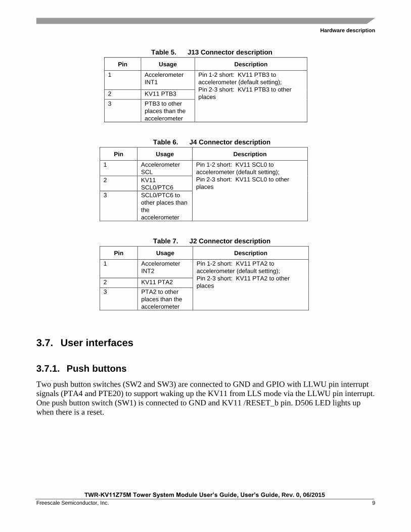
Table 5. J13 Connector description
Pin Usage Description
1 Accelerometer
INT1
Pin 1-2 short: KV11 PTB3 to
accelerometer (default setting);
Pin 2-3 short: KV11 PTB3 to other
places 2 KV11 PTB3
3 PTB3 to other
places than the
accelerometer
Table 6. J4 Connector description
Pin Usage Description
1 Accelerometer
SCL
Pin 1-2 short: KV11 SCL0 to
accelerometer (default setting);
Pin 2-3 short: KV11 SCL0 to other
places 2 KV11
SCL0/PTC6
3 SCL0/PTC6 to
other places than
the
accelerometer
Table 7. J2 Connector description
Pin Usage Description
1 Accelerometer
INT2
Pin 1-2 short: KV11 PTA2 to
accelerometer (default setting);
Pin 2-3 short: KV11 PTA2 to other
places 2 KV11 PTA2
3 PTA2 to other
places than the
accelerometer
3.7. User interfaces
3.7.1. Push buttons
Two push button switches (SW2 and SW3) are connected to GND and GPIO with LLWU pin interrupt
signals (PTA4 and PTE20) to support waking up the KV11 from LLS mode via the LLWU pin interrupt.
One push button switch (SW1) is connected to GND and KV11 /RESET_b pin. D506 LED lights up
when there is a reset.
Hardware description
TWR-KV11Z75M Tower System Module User’s Guide, User’s Guide, Rev. 0, 06/2015
10 Freescale Semiconductor, Inc.
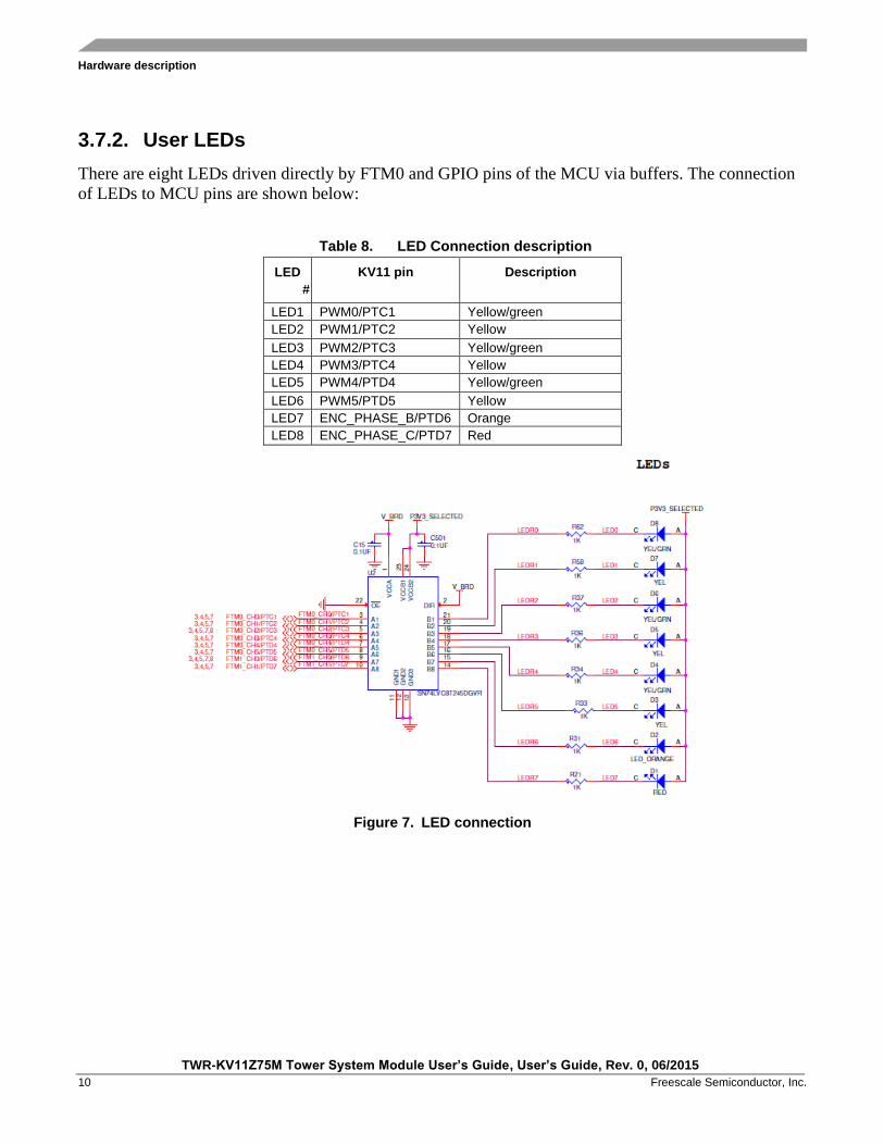
3.7.2. User LEDs
There are eight LEDs driven directly by FTM0 and GPIO pins of the MCU via buffers. The connection
of LEDs to MCU pins are shown below:
Table 8. LED Connection description
LED
#
KV11 pin Description
LED1 PWM0/PTC1 Yellow/green
LED2 PWM1/PTC2 Yellow
LED3 PWM2/PTC3 Yellow/green
LED4 PWM3/PTC4 Yellow
LED5 PWM4/PTD4 Yellow/green
LED6 PWM5/PTD5 Yellow
LED7 ENC_PHASE_B/PTD6 Orange
LED8 ENC_PHASE_C/PTD7 Red
Figure 7. LED connection
Hardware description
TWR-KV11Z75M Tower System Module User’s Guide, User’s Guide, Rev. 0, 06/2015
Freescale Semiconductor, Inc. 11
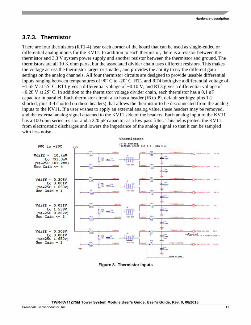
3.7.3. Thermistor
There are four thermistors (RT1-4) near each corner of the board that can be used as single-ended or
differential analog inputs for the KV11. In addition to each thermistor, there is a resistor between the
thermistor and 3.3 V system power supply and another resistor between the thermistor and ground. The
thermistors are all 10 K ohm parts, but the associated divider chain uses different resistors. This makes
the voltage across the thermistor larger or smaller, and provides the ability to try the different gain
settings on the analog channels. All four thermistor circuits are designed to provide useable differential
inputs ranging between temperatures of 90˚ C to -20˚ C. RT2 and RT4 both give a differential voltage of
~1.65 V at 25˚ C. RT1 gives a differential voltage of ~0.10 V, and RT3 gives a differential voltage of
~0.28 V at 25˚ C. In addition to the thermistor voltage divider chain, each thermistor has a 0.1 uF
capacitor in parallel. Each thermistor circuit also has a header (J6 to J9, default settings: pins 1-2
shorted, pins 3-4 shorted on these headers) that allows the thermistor to be disconnected from the analog
inputs to the KV11. If a user wishes to apply an external analog value, these headers may be removed,
and the external analog signal attached to the KV11 side of the headers. Each analog input to the KV11
has a 100 ohm series resistor and a 220 pF capacitor as a low pass filter. This helps protect the KV11
from electrostatic discharges and lowers the impedance of the analog signal so that it can be sampled
with less noise.
Figure 8. Thermistor inputs
Hardware description
TWR-KV11Z75M Tower System Module User’s Guide, User’s Guide, Rev. 0, 06/2015
12 Freescale Semiconductor, Inc.
3.8. Interface connectors
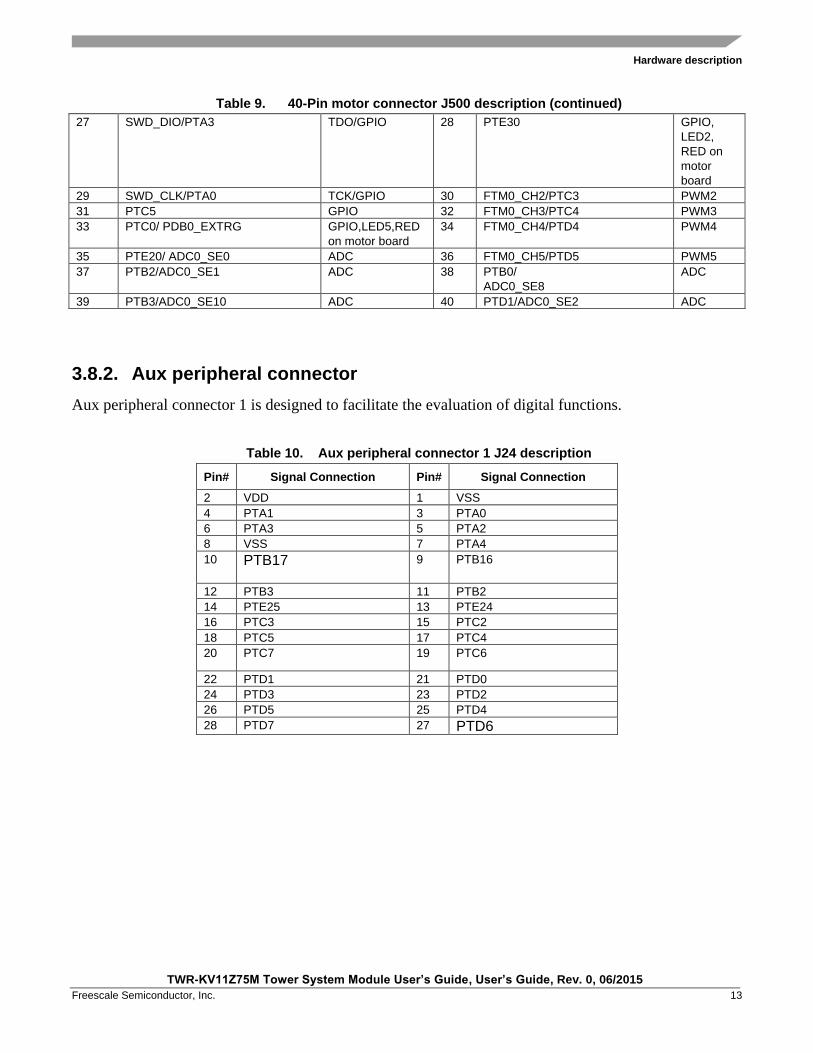
3.8.1. Motor connector
The KV11 board can be connected to a motor control board such as APMOTOR56F8000E. The motor
control connector (female) is located on the bottom of the board.
Some KV11 pins are connected to the motor control connector. Those pins, associated with analog
inputs, have 100 ohm resistors in series to provide some ESD protection for the analog inputs of the
KV11. The pins, providing analog signals from the motor control board, have 220 pF caps with the
resistors to provide a low pass filter. The connector pin out is shown in Table 11. Aux peripheral
connector 2 J18 description.
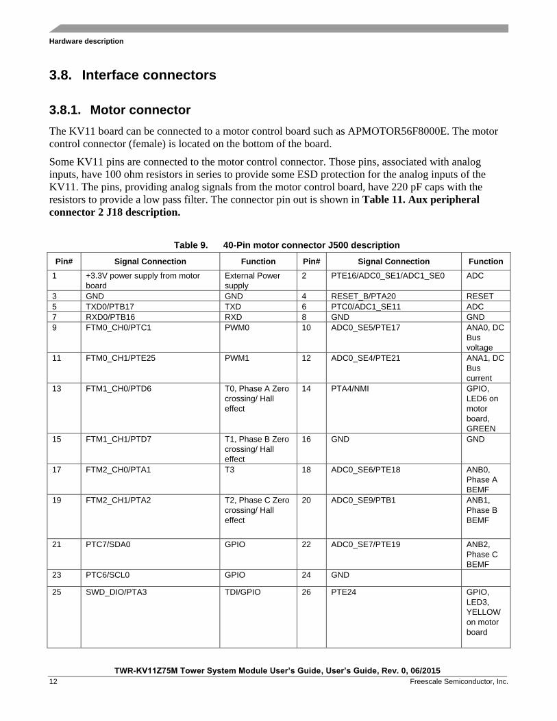
Table 9. 40-Pin motor connector J500 description
Pin# Signal Connection Function Pin# Signal Connection Function
1 +3.3V power supply from motor
board
External Power
supply
2 PTE16/ADC0_SE1/ADC1_SE0 ADC
3 GND GND 4 RESET_B/PTA20 RESET
5 TXD0/PTB17 TXD 6 PTC0/ADC1_SE11 ADC
7 RXD0/PTB16 RXD 8 GND GND
9 FTM0_CH0/PTC1 PWM0 10 ADC0_SE5/PTE17 ANA0, DC
Bus
voltage
11 FTM0_CH1/PTE25 PWM1 12 ADC0_SE4/PTE21 ANA1, DC
Bus
current
13 FTM1_CH0/PTD6
T0, Phase A Zero
crossing/ Hall
effect
14 PTA4/NMI GPIO,
LED6 on
motor
board,
GREEN
15 FTM1_CH1/PTD7
T1, Phase B Zero
crossing/ Hall
effect
16 GND GND
17 FTM2_CH0/PTA1 T3 18 ADC0_SE6/PTE18 ANB0,
Phase A
BEMF
19 FTM2_CH1/PTA2 T2, Phase C Zero
crossing/ Hall
effect
20 ADC0_SE9/PTB1 ANB1,
Phase B
BEMF
21 PTC7/SDA0 GPIO 22 ADC0_SE7/PTE19 ANB2,
Phase C
BEMF
23 PTC6/SCL0 GPIO 24 GND
25 SWD_DIO/PTA3 TDI/GPIO 26 PTE24 GPIO,
LED3,
YELLOW
on motor
board
Hardware description
TWR-KV11Z75M Tower System Module User’s Guide, User’s Guide, Rev. 0, 06/2015
Freescale Semiconductor, Inc. 13
Table 9. 40-Pin motor connector J500 description (continued)
27 SWD_DIO/PTA3 TDO/GPIO 28 PTE30 GPIO,
LED2,
RED on
motor
board
29 SWD_CLK/PTA0 TCK/GPIO 30 FTM0_CH2/PTC3 PWM2
31 PTC5 GPIO 32 FTM0_CH3/PTC4 PWM3
33 PTC0/ PDB0_EXTRG GPIO,LED5,RED
on motor board
34 FTM0_CH4/PTD4 PWM4
35 PTE20/ ADC0_SE0 ADC 36 FTM0_CH5/PTD5 PWM5
37 PTB2/ADC0_SE1 ADC 38 PTB0/
ADC0_SE8
ADC
39 PTB3/ADC0_SE10 ADC 40 PTD1/ADC0_SE2 ADC
3.8.2. Aux peripheral connector
Aux peripheral connector 1 is designed to facilitate the evaluation of digital functions.
Table 10. Aux peripheral connector 1 J24 description
Pin# Signal Connection Pin# Signal Connection
2 VDD 1 VSS
4 PTA1 3 PTA0
6 PTA3 5 PTA2
8 VSS 7 PTA4
10 PTB17
9 PTB16
12 PTB3 11 PTB2
14 PTE25 13 PTE24
16 PTC3 15 PTC2
18 PTC5 17 PTC4
20 PTC7 19 PTC6
22 PTD1 21 PTD0
24 PTD3 23 PTD2
26 PTD5 25 PTD4
28 PTD7 27 PTD6
TWR-KV11Z75M Options and headers
TWR-KV11Z75M Tower System Module User’s Guide, User’s Guide, Rev. 0, 06/2015
14 Freescale Semiconductor, Inc.
The aux peripheral connecter 2 is designed to facilitate the evaluation of analog functions.
Table 11. Aux peripheral connector 2 J18 description
Pin# Signal Connection Pin# Signal Connection
2 VDDA 1 VSSA
4 VREFH 3 VREFL
6 PTE17/ADC0_SE5/ADC1_SE5 5 PTE16/ADC0_SE1
8 PTE19/ADC0_SE7/ADC1_SE7 7 PTE18/ADC0_SE6
10 PTE21/ADC0_SE4 9 PTE20/ADC0_SE0
12 PTE29/ CMP0_IN5/CMP1_IN5 11 PTE30/ADC1_SE4
14 PTC1/ADC1_SE3 13 PTC0/ ADC1_SE11
16 PTC3/CMP1_IN1 15 PTC2/ADC0_SE11
18 PTB1/ ADC1_SE9 17 PTB0/ ADC0_SE8
20 PTB3/ADC1_SE2 19 PTB2/ADC0_SE10
4. TWR-KV11Z75M Options and headers
The following is a list of all the jumper options. The default installed jumper settings are indicated by
the text within the blue boxes.
Table 11. TWR-KV11Z75M Jumper table
Jumper Option Setting Description
J1 PTC3 select ON Connect PTC3 to J24 A38 and B47pin
OFF Connect PTC3 to J24 B47 pin only
J2 PTA2 selection 1-2 Connect PTA2 to FXOS87000CQ
2-3 Connect PTA2 to elevator J24 and auxiliary connector J6
J4 I2C0 SCL0(PTC6) selection 1-2 Connect SCL0 to elevator J24 A7 pin and J6
2-3 Connect this pin to accelerometer(U6)
J5 CAN signal selector
1-2 Enable pull-down to CAN - C_SLEEP signal
3-4 Connect PTA13 toCAN - C_SLEEP signa
5-6 Connect PTE25 to C_RXD signal
7-8 Connect PTE24 to C_TXD signal
9-10 Enable 120 ohm resistor load between CANL-CANH signals
J6
RT4 connection with KV11
PTB3
1-2 Connect one terminal of RT4 to KV11 PTB3 pin
OPEN Connect one terminal of RT3 to KV11 PTB3 pin
RT4 connection with KV11
PTB2
3-4 Connect one terminal of RT3 to KV11 PTB2 pin
Open Connect one terminal of RT3 to KV11 PTB2 pin
TWR-KV11Z75M Options and headers
TWR-KV11Z75M Tower System Module User’s Guide, User’s Guide, Rev. 0, 06/2015
Freescale Semiconductor, Inc. 15
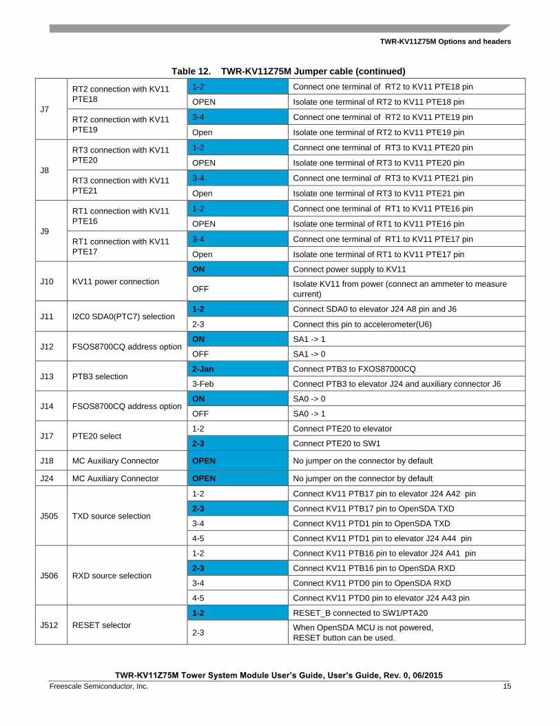
Table 12. TWR-KV11Z75M Jumper cable (continued)
J7
RT2 connection with KV11
PTE18
1-2 Connect one terminal of RT2 to KV11 PTE18 pin
OPEN Isolate one terminal of RT2 to KV11 PTE18 pin
RT2 connection with KV11
PTE19
3-4 Connect one terminal of RT2 to KV11 PTE19 pin
Open Isolate one terminal of RT2 to KV11 PTE19 pin
J8
RT3 connection with KV11
PTE20
1-2 Connect one terminal of RT3 to KV11 PTE20 pin
OPEN Isolate one terminal of RT3 to KV11 PTE20 pin
RT3 connection with KV11
PTE21
3-4 Connect one terminal of RT3 to KV11 PTE21 pin
Open Isolate one terminal of RT3 to KV11 PTE21 pin
J9
RT1 connection with KV11
PTE16
1-2 Connect one terminal of RT1 to KV11 PTE16 pin
OPEN Isolate one terminal of RT1 to KV11 PTE16 pin
RT1 connection with KV11
PTE17
3-4 Connect one terminal of RT1 to KV11 PTE17 pin
Open Isolate one terminal of RT1 to KV11 PTE17 pin
J10 KV11 power connection
ON Connect power supply to KV11
OFF Isolate KV11 from power (connect an ammeter to measure
current)
J11 I2C0 SDA0(PTC7) selection 1-2 Connect SDA0 to elevator J24 A8 pin and J6
2-3 Connect this pin to accelerometer(U6)
J12 FSOS8700CQ address option ON SA1 -> 1
OFF SA1 -> 0
J13 PTB3 selection 2-Jan Connect PTB3 to FXOS87000CQ
3-Feb Connect PTB3 to elevator J24 and auxiliary connector J6
J14 FSOS8700CQ address option ON SA0 -> 0
OFF SA0 -> 1
J17 PTE20 select 1-2 Connect PTE20 to elevator
2-3 Connect PTE20 to SW1
J18 MC Auxiliary Connector OPEN No jumper on the connector by default
J24 MC Auxiliary Connector OPEN No jumper on the connector by default
J505 TXD source selection
1-2 Connect KV11 PTB17 pin to elevator J24 A42 pin
2-3 Connect KV11 PTB17 pin to OpenSDA TXD
3-4 Connect KV11 PTD1 pin to OpenSDA TXD
4-5 Connect KV11 PTD1 pin to elevator J24 A44 pin
J506 RXD source selection
1-2 Connect KV11 PTB16 pin to elevator J24 A41 pin
2-3 Connect KV11 PTB16 pin to OpenSDA RXD
3-4 Connect KV11 PTD0 pin to OpenSDA RXD
4-5 Connect KV11 PTD0 pin to elevator J24 A43 pin
J512 RESET selector
1-2 RESET_B connected to SW1/PTA20
2-3 When OpenSDA MCU is not powered,
RESET button can be used.
Revision History
TWR-KV11Z75M Tower System Module User’s Guide, User’s Guide, Rev. 0, 06/2015
16 Freescale Semiconductor, Inc.
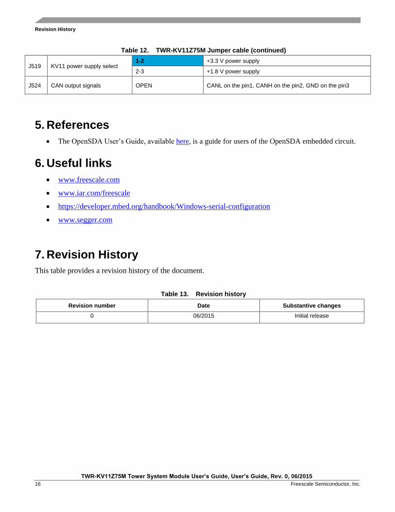
Table 12. TWR-KV11Z75M Jumper cable (continued)
J519 KV11 power supply select 1-2 +3.3 V power supply
2-3 +1.8 V power supply
J524 CAN output signals OPEN CANL on the pin1, CANH on the pin2, GND on the pin3
5. References
The OpenSDA User’s Guide, available here, is a guide for users of the OpenSDA embedded circuit.
6. Useful links
www.freescale.com
www.iar.com/freescale
https://developer.mbed.org/handbook/Windows-serial-configuration
www.segger.com
7. Revision History
This table provides a revision history of the document.
Table 13. Revision history
Revision number Date Substantive changes
0 06/2015 Initial release
Document Number: TWRKV11Z75MUG Rev. 0
06/2015
How to Reach Us:
Home Page:
freescale.com
Web Support:
freescale.com/support
Information in this document is provided solely to enable system and software implementers to
use Freescale products. There are no express or implied copyright licenses granted hereunder to
design or fabricate any integrated circuits based on the information in this document.
Freescale reserves the right to make changes without further notice to any products herein.
Freescale makes no warranty, representation, or guarantee regarding the suitability of its
products for any particular purpose, nor does Freescale assume any liability arising out of the
application or use of any product or circuit, and specifically disclaims any and all liability,
including without limitation consequential or incidental damages. “Typical” parameters that may
be provided in Freescale data sheets and/or specifications can and do vary in different
applications, and actual performance may vary over time. All operating parameters, including
“typicals,” must be validated for each customer application by customer's technical experts.
Freescale does not convey any license under its patent rights nor the rights of others. Freescale
sells products pursuant to standard terms and conditions of sale, which can be found at the
following address: freescale.com/SalesTermsandConditions.
Freescale, the Freescale logo, and Kinetis are trademarks of Freescale Semiconductor, Inc.
Tower is are trademark of Freescale Semiconductor, Inc. All other product or service names are
the property of their respective owners. ARM and Cortex are registered trademarks of ARM
Limited (or its subsidiaries) in the EU and/or elsewhere. mbed is a trademark of ARM Limited
(or its subsidiaries) in the EU and/or elsewhere. All rights reserved.
© 2015 Freescale Semiconductor, Inc.