tutorial indonesia final - sweetsweet.ua.pt/iouliia/papers/2006/iiwas_tutorial.pdf · karen...
TRANSCRIPT


G. Estrin, “Organization of Computer Systems – The Fixed Plus Variable Structure Computer”, Proc. Western Joint Computer Conf., New York, 1960, pp. 33-40.G. Estrin, “Reconfigurable Computer Origins: The UCLA Fixed-Plus-Variable (F+V) Structure Computer”, IEEE Annals of the History of Computing, 2002, pp. 3-9.
F VIn/Out
SupervisoryControl
Humans
A new way to evolve higherperformance computing from
any general purpose computer
Fixed + Variable structure computer
A standard processorF augmented by
an array of reconfigurablehardware V
Flexibility of software+
the speed of hardware

1947 Shockley, et al. – the first transistor at Bell Labs;1958 Jack Kilby – the first integrated circuit;1959-1960 G. Estrin, Reconfigurable Computer Origins;1962 Hofstein, et al. - metal-oxide semiconductor field-
effect transistor (MOSFET);1970 Intel – the first 1024-bit DRAM;1970 Fairchild – the first 256-bit SRAM;1970 Ron Cline (Signetics) – the first PLD (PLA);1971 Intel – the first microprocessor, 4004;1978 Monolithic Memories Inc. – the first PAL;1984 Altera – the first CPLD based on a combination of
CMOS and EPROM technologies;1985 Xilinx - the first FPGA, the XC2064™ - a
radical new form of programmable logic;1991 The world's first commercial reconfigurable
computer, the Algotronix CHS2X4

1. EE Times, “Semiconductor FPGA/PLD market to grow 14% in '06”, posted 30 May, 2006, available at: http://www.eetasia.com/ART_8800419580_499485_0e42dd84200605.HTM.
The market for FPGAs and other PLD is expected to grow from $3.2 billion in 2005 to $6.7 billion in 2010, according to Gartner Dataquest [1].
The FPGA/PLD market is dominated by Xilinx Inc. and AlteraCorp. (84% of the market in 2005 [1]).
Gartner's numbers contrast with those of In-Stat predicting the FPGA market to grow from $1.9 billion in 2005 to $2.75 billion in 2010 [1].
In-Stat's forecast covers only FPGAs, while the Garter forecast includes other PLDs.

Some interesting facts from [1]:
1. EE Times, “FPGA Market Will Reach $2.75 Billion by Decade's End”, posted 24 May, 2006, available at: http://www.us.design-reuse.com/news/news13441.html.
→ The largest FPGA consumers will be communications and industrial, whose combine market share of the FPGA market will increase from 73.8% in 2005, to 76.8% by 2010.
→ FPGAs find numerous applications in the scope of electronic system design, from glue logic to high-complexity application specific (ASIC-type) devices.
→ Pioneering products such as Xilinx’s Virtex or Altera’s Stratix families willfind their main applications in the development of high-volume products.

1. Karen Parnell, Roger Bryner, “Comparing and Contrasting FPGA and Microprocessor System Design and Development”, WP213 (v1.1) July 21, 2004. Available at: http://direct.xilinx.com/bvdocs/whitepapers/wp213.pdf
0%
10%
20%
30%
40%
50%
60%
Xilinx Altera Lattice Actel QuickLogic
Others
Xilinx – 51%, Altera – 32%, Lattice – 8%, Actel – 6%, QuickLogic – 2%, Others – 1%.

1. Karen Parnell, Roger Bryner, “Comparing and Contrasting FPGA and Microprocessor System Design and Development”, WP213 (v1.1) July 21, 2004. Available at: http://direct.xilinx.com/bvdocs/whitepapers/wp213.pdf
0%
10%
20%
30%
40%
50%
60%
Xilinx All others
Xilinx – 59%, All others – 41%.

1984. Ross Freeman, Bernie Vonderschmitt, and Jim Barnett found Xilinx.1985. Xilinx introduces its first product, the FPGA XC2064™.1991. The XC4000™ family of FPGAs is introduced.1998.Virtex™ FPGA family is introduced (Virtex / E / EM).1999. New low power and lower cost CPLD products.2001. Virtex ™-II family – the first platform FPGA.2003. Spartan™-3 family of products is introduced - the world's first 90nm FPGA. 2004. Virtex™-4 family of products is introduced (multi-platform FPGA family).2006. Virtex™-5 family of products is introduced - the world's first 65nm FPGA.
1. History of Xilinx. Available at: http://direct.xilinx.com/company/history.htm2. Virtex™ Family FPGAs: Highest System Performance. Available at:
http://www.xilinx.com/products/silicon_solutions/fpgas/virtex/index.htm3. Xilinx Earns Highest Ratings in FPGA Vendor Survey. Available at:: http://www.hpcwire.com/hpc/786279.html
In January, 2003, Xilinx was named number four on Fortune magazine's "100 Best Companies to Work For
in America" list.
0
2
4
6
8
10
12
14
2001 2002 2003 2004 2005
Xilinx Inc. took top honors for the third consecutive year in the FPGA EDA tool vendor survey conducted by EE Times in 2006 [3].

1. Revolutionary Architecture for the Next Generation Platform FPGAs, December 8, 2003. Available at: http://www.xilinx.com/company/press/kits/asmbl/asmbl_arch_pres.pdf.
2. Moore’s low. Available at: http://www.intel.com/technology/mooreslaw/index.htm. 3. Ralph H.J.M. Otten, Paul Stravers. Challenges in Physical Chip Design. Available at:
http://delivery.acm.org/10.1145/610000/602923/p84-otten.pdf?key1=602923&key2=5142353611&coll= GUIDE&dl=GUIDE&CFID=4553126&CFTOKEN=37443806
4. Available at: http://conferences.ece.ubc.ca/isfpga2007/www/2006/panel.html
4004 (1971) – 2300;8080 (1974) – 4500;8086 (1978) – 29000;Intel286 (1982) – 134000;Intel386 (1985) – 275000;Intel486 (1989) – 1.2×10⁶;Pentium (1993) – 3.1 ×10⁶;Pentium II (1997) – 7.5 ×10⁶;Pentium III (1999) – 9.5 ×10⁶.
Num
ber o
f tra
nsis
tors
×10
8
123456789
1011
Year1990 2000 2010
1G
64M
256M
Static memory
Virtex
Virt
ex-E
Virt
ex-II Virt
ex-II
Pro
Virt
ex-4
-5
Xilinx FPGA
Itanium 2 (9MB cache)
Intel processors
Pentium 4
Itanium 2
Dual core
“Moore’s law has allowed vendors to produce new FPGAs every two years with generally double the density, better performance, and improved features” [4]


• Programmable Logic Devices - PLD;• Field Programmable Gate Arrays - FPGA;• FPGA architectures;• Platform FPGA;• Multi-platform FPGA;• System-on-chip;• Network-on-chip;• Reconfigurable computing;• Reconfigurable systems.

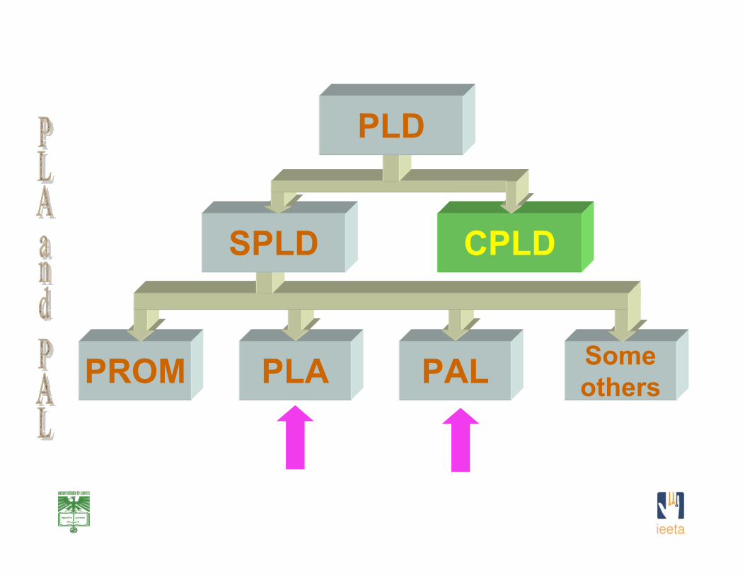
SomeothersPALPLAPROM
SPLD CPLD
PLD

BCD tosegments
BCD y1y2
y7
abcd
0 0 0 0 1 1 1 1 1 1 00 0 0 1 0 1 1 0 0 0 00 0 1 0 1 1 0 1 1 0 10 0 1 1 1 1 1 1 0 0 10 1 0 0 0 1 1 0 0 1 10 1 0 1 1 0 1 1 0 1 10 1 1 0 1 0 1 1 1 1 10 1 1 1 1 1 1 0 0 0 01 0 0 0 1 1 1 1 1 1 11 0 0 1 1 1 1 1 0 1 1
a b c d y1 y2 y3 y4 y5 y6 y7
BCD segments
1 (y1)2y2
3y3
y5= abcd ∨ abcd ∨ abcd ∨ abcd;4 variables

0 0 0 0 1 1 1 1 1 1 00 0 0 1 0 1 1 0 0 0 00 0 1 0 1 1 0 1 1 0 10 0 1 1 1 1 1 1 0 0 10 1 0 0 0 1 1 0 0 1 10 1 0 1 1 0 1 1 0 1 10 1 1 0 1 0 1 1 1 1 10 1 1 1 1 1 1 0 0 0 01 0 0 0 1 1 1 1 1 1 11 0 0 1 1 1 1 1 0 1 1
a b c d y1 y2 y3 y4 y5 y6 y7
BCD segments
address
RAM/ROM(PROM)
a b c d
y1 y2 y3 y4 y5 y6 y7
data
SomeothersPALPLAPROM
SPLD CPLD
PLD

y5= abcd ∨ abcd ∨ abcd ∨ abcd;y5= bcd ∨ acd;
a
b
c
d
y5

Beginy1
y2
x1
x2
End
1
10
0
y3,y4y3
a0
a1
a2 a3
a0
a0
a1
a2 a3
y1
y2
y3 y3,y4
1
x1
x1
x1
x1x2
x1x2x 1x 2
x 1x 2 x1x2
x1 x
2
a0 00 a1 01 1 D2y1a1 01 a0 00 x1 -y2 a2 10 x1x2 D1
a3 11 x1x2 D1D2a2 10 a0 00 x1 -y3 a2 10 x1x2 D1
a3 11 x1x2 D1D2a3 11 a0 00 x1 -y3 a2 10 x1x2 D1y4 a3 11 x1x2 D1D2
A trivial algorithm that enables us to count the
number of ones in a binary vector

F1F2
y1y2y3y4D1
D2
x1
x2

CPLD
SomeothersPALPLAPROM
SPLD
PLD

SPLD SPLD
Programmable interconnect matrix
SPLDSPLD
I/O I/O
I/O I/O
CPLD were introducedby Altera in 1984
EP300 PLDs introduced—world’s first reprogrammable PLD and first commercial programmable logic device patent. 20 years of Altera innovations. Available at: http://media.corporate-ir.net/media_files/irol/83/83265/2003ar.pdf

1. Karen Parnell & Nick Mehta, Programmable Logic Design Quick Start Hand Book. Available at: http://www.xilinx.com/publications/products/cpld/logic_handbook.pdf
I/OMcells PLA PLA I/O
Mcells
Pro
gram
mab
lein
terc
onne
ctm
atrix
(PIM
)
Logic block Logic blocki/o
i/o
i/o
i/o
16 Mcells per Logic block The design software hides the CPLD resources, which enables end users to work with higher level constructs and to abstract from the architectural details
2-24 Logic blocks per device
Each logic block – 36 x 48 PLA

1. Karen Parnell & Nick Mehta, Programmable Logic Design Quick Start Hand Book (2006). Available at: http://www.xilinx.com/publications/products/cpld/logic_handbook.pdf
1985 1990 1995 from 2000
Per
form
ance
and
Den
sity
CountersFSMs
Memory controllers,Bus interfaces,UARTs
High speed clocking,Delay lock loops,Digital delay lines
Cell phones,Cameras,DVD players,Portable GPS,PDAs,Home networking,MP3,Printers,Prototyping boards, controllers,Graphics cards,etc.

CLBCLB
PIPI
CLBCLB
PIPI
CLBCLB
PIPI
PIPI
PIPI
PIPI
PIPI
CLBCLB
PIPI
CLBCLB
PIPI
CLBCLB
PIPI
PIPI
PIPI
PIPI
PIPI
CLBCLB
PIPI
CLBCLB
PIPI
CLBCLB
CLBCLB Configurable Logic Block PIPI Programmable Interconnect

CLBCLB• Number and functionality of CLBs vary from device to device;
• Each CLB consists of a configurable switch matrix with 4 or 6 inputs,flip-flops and selection circuits;
• The switch matrix is very flexible and can be configured to handle combinatorial logic, shift registers, or RAM.
Getting Started with FPGAs. Available at: http://www.xilinx.com/company/gettingstarted/index.htm
PIPI
• PI makes routes between CLBs (IOBs) allowing to construct verycomplicated circuits and to provide an external interface with the circuit;
• The design software takes care about all the details and makes the interconnect routing task hidden to users.
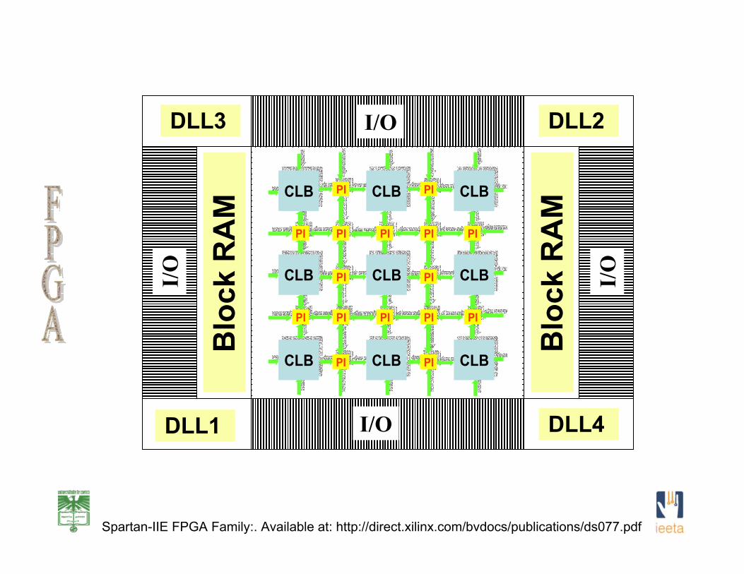
Spartan-IIE FPGA Family:. Available at: http://direct.xilinx.com/bvdocs/publications/ds077.pdf
Blo
ck R
AM
Blo
ck R
AM
DLL1
DLL2DLL3
DLL0
I/O
I/O
CLBCLB
PIPI
CLBCLB
PIPI
CLBCLB
PIPI
PIPI
PIPI
PIPI
PIPI
CLBCLB
PIPI
CLBCLB
PIPI
CLBCLB
PIPI
PIPI
PIPI
PIPI
PIPI
CLBCLB
PIPI
CLBCLB
PIPI
CLBCLB
I/O
Blo
ck R
AM
Blo
ck R
AM
DLL4
DLL2
DLL1
DLL3
I/O

Address2
Address1 Block RAM Data1
Data2
4096 × 1 2048 × 21024 × 4 512 × 8
256 × 16From 8 to 72 blocks
1. Eliminates skew;2. Provides four phases of
the clock;3. Doubles the clock;4. Divides the clock by 1.5,
2, 2.5, 3, 4, 5,8 or 16
DLLCLK0CLK90CLK180CLK270
Spartan-IIE FPGA Family:. Available at: http://direct.xilinx.com/bvdocs/publications/ds077.pdf

Standard FPGAs, which are targeted at multiple applications such as embedded systems, digital signal processing, etc. [1]
Multiple FPGA platforms make possible a specific platform to be optimizedspecifically for a certain domain of applications – such as logic, connectivity,DSP and embedded processing – to meet application requirements previously delivered only by ASICs while remaining programmable at heart [2]
1. Glossary of Terms. Available at: http://www.xilinx.com/company/terms.htm
2. Karen Parnell & Nick Mehta, Programmable Logic Design Quick Start Hand Book (2006). Available at: http://www.xilinx.com/publications/products/cpld/logic_handbook.pdf

CLBCLB
PIPI
CLBCLB
PIPI
CLBCLB
PIPI
PIPI
PIPI
PIPI
PIPI
CLBCLB
PIPI
CLBCLB
PIPI
CLBCLB
PIPI
PIPI
PIPI
PIPI
PIPI
CLBCLB
PIPI
CLBCLB
PIPI
CLBCLB
CLBCLB
PIPI
CLBCLB
PIPI
CLBCLB
PIPI
PIPI
PIPI
PIPI
PIPI
CLBCLB
PIPI
CLBCLB
PIPI
CLBCLB
PIPI
PIPI
PIPI
PIPI
PIPI
CLBCLB
PIPI
CLBCLB
PIPI
CLBCLB
CLBCLB
PIPI
CLBCLB
PIPI
CLBCLB
PIPI
PIPI
PIPI
PIPI
PIPI
CLBCLB
PIPI
CLBCLB
PIPI
CLBCLB
PIPI
PIPI
PIPI
PIPI
PIPI
CLBCLB
PIPI
CLBCLB
PIPI
CLBCLB
CLBCLB
PIPI
CLBCLB
PIPI
CLBCLB
PIPI
PIPI
PIPI
PIPI
PIPI
CLBCLB
PIPI
CLBCLB
PIPI
CLBCLB
PIPI
PIPI
PIPI
PIPI
PIPI
CLBCLB
PIPI
CLBCLB
PIPI
CLBCLB
I/OI/
O
I/O
I/O
Spartan-3 Architecture Layout [1]
1. Xilinx Spartan-3 FPGA Family: Complete Data Sheet. Available at: http://direct.xilinx.com/bvdocs/publications/ds099.pdf
DCMDCM
DCMDCM
Multiplier Block RAM MultiplierBlock RAM

CLBCLB
PIPI
Spartan-3 CLB = 4 slices
Each slice includes:• Two RAM-based logic function generators (two Look-Up Tables – LUTs );• Two storage elements (D-type flip-flop or a level-sensitive latch); • wide-function multiplexers; • carry logic;• arithmetic gates.
1. Xilinx Spartan-3 FPGA Family: Complete Data Sheet. Available at: http://direct.xilinx.com/bvdocs/publications/ds099.pdf
LUT can be configured as distributed RAM or a 16-bit shift register.
There are four types of interconnect, which passes signals amongthe functional elements. They are optimized for different clock frequencies, provide higher or smaller routing flexibilities, etc.
0 0 0 0 10 0 0 1 00 0 1 0 10 0 1 1 10 1 0 0 00 1 0 1 10 1 1 0 10 1 1 1 11 0 0 0 11 0 0 1 1
a b c d F

The DCM supports three major functions [1]:• Clock-skew Elimination;• Frequency Synthesis;• Phase Shifting.
1. Xilinx Spartan-3 FPGA Family: Complete Data Sheet. Available at: http://direct.xilinx.com/bvdocs/publications/ds099.pdf
From 4 to 104 18Kbit configurable, synchronous dual-port RAM blocks
From 4 to 104 embedded multipliers.Each multiplier takes two 18-bit
operands and produces a 36-bit product
From 2 to 4 DCMs

1. Xilinx Virtex-4 Family Overview. Available at: http://www.xilinx.com/bvdocs/publications/ds112.pdf2. Karen Parnell & Nick Mehta, Programmable Logic Design Quick Start Hand Book (2006). Available at: http://www.xilinx.com/publications/products/cpld/logic_handbook.pdf.
Virtex-4 Multi-platform FPGA Family [2]
Feature CFeature C
Feature BFeature B
Feature AFeature A
Feature CFeature C
Feature AFeature A
Advanced Silicon Modular Block (ASMBLTM) columnar architecture [1,2]
Feature CFeature C
Feature BFeature B
Feature AFeature A

1. Xilinx Virtex-4 Family Overview. Available at: http://www.xilinx.com/bvdocs/publications/ds112.pdf
Virtex-4 Multi-platform FPGA Family [1]
• LX: High-performance logic applications;
• SX: High-performance solution for digital signalprocessing (DSP);
• FX: High-performance, full-featured solution forembedded platform applications.

LX
SX
FXMax number of DSP
LX
SX
FXMax block memory
LX
SX
FXMax number of DCM
FXMax number of PowerPC
LX
SX
FXMax number of slices
FXRocketIO transceiver blocks
LX: high-performance logic; SX: High-performance DSP;FX: Embedded applications
1. Xilinx Virtex-5 Family Overview. Available at: http://www.xilinx.com/bvdocs/publications/ds100.pdf
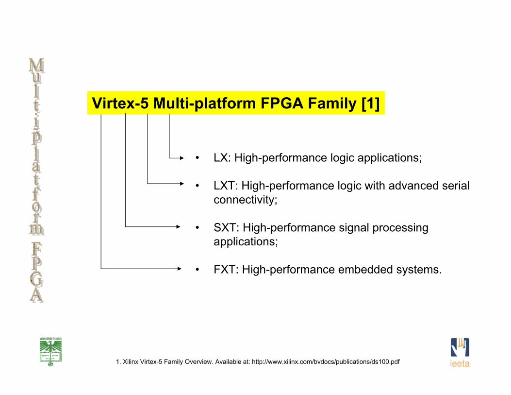
Virtex-5 Multi-platform FPGA Family [1]
• LX: High-performance logic applications;
• LXT: High-performance logic with advanced serial connectivity;
• SXT: High-performance signal processing applications;
• FXT: High-performance embedded systems.

1. Altera Product Catalog. October 2006. Available at: http://www.altera.co.jp/literature/sg/product-catalog.pdf
The Cyclon II FPGA family (90 nm) [1]
Phase-Locked Loops (PLL).Embedded Multipliers.Logic Array.M4K Memory Blocks.I/O Elements.

The Stratix III FPGA family (65 nm) [1]
L – Balanced logic, memory and DSP for general-purpose applications;E – Enhanced memory and DSP for DSP intensive applications;GX – Integrated transceivers for high bandwidth interface applications.
1. Altera Product Catalog. October 2006. Available at: http://www.altera.co.jp/literature/sg/product-catalog.pdf

1. The Programmable Logic Data Book. Xilinx, Inc., 1999.2. Achronix Semiconductor Announces 1.93 GHz 90nm 'ULTRA' FPGA Prototype First Silicon Success. APRIL 26 2006. Available at:
http://www.dsp-fpga.com/news/db/?26143. Xilinx Spartan-3 FPGA Family: Complete Data Sheet. Available at: http://direct.xilinx.com/bvdocs/publications/ds099.pdf
XC4000 FPGAs – system clock up to 80 MHz [1]
The fastest FPGAs of Achronix Semiconductor –up to 1.93 GHz [2]
Spartan FPGAs – Maximum system gates – 40K = 40 000 [1]
Spartan-3 FPGA – Maximum system gates – 5M = 5 000 000 [3]

0
500000
1000000
1500000
2000000
2500000
3000000
3500000
4000000
4500000
5000000
Spartan Spartan-II Spartan-IIE
Spartan-3
Max System Gates
0
1000
2000
3000
4000
5000
6000
7000
8000
9000
Spartan Spartan-II Spartan-IIE
Spartan-3
Max CLBs

0
100
200
300
400
500
600
Spartan Spartan-II Spartan-IIE
Spartan-3 Virtex-5
System Performance
Clo
ck (M
Hz)

0
2000
4000
6000
8000
10000
12000
S S-II S-IIE S-3 V-II V-IIPro V-4 V-5
Max Block RAM
Kbi
ts

1. About Structured ASICs. Available at: http://www.altera.com/products/devices/hardcopy/articles/hrd-articles.html2. Structured ASIC Design Flow Available at: http://www.altera.com/products/software/flows/asic/qts-structured_asic.html3. HardCopy Structured ASICs: ASIC Gain Without the Pain. Available at: http://www.altera.com/products/devices/hardcopy/hrd-index.html
“Structured ASICs leverage standard-cell technology and the most advanced semiconductor processes to embed logic and hard functions—such as memory, phase-locked loops (PLLs), clock networks, and power bussing—into pre-engineered, pre-verified base layers. The structured ASIC is customized using just the top metal layers” [1].
All layers ofstandard-cell
ASIC arecustom
All layers ofstandard-cell
ASIC arecustom
Customizationthrough top
layers instructured ASICs
Customizationthrough top
layers instructured ASICs
Pre-designed base layers with embedded logic
and reusable circuits

1. Structured ASIC Design Flow Available at: http://www.altera.com/products/software/flows/asic/qts-structured_asic.html2. HardCopy Structured ASICs: ASIC Gain Without the Pain. Available at: http://www.altera.com/products/devices/hardcopy/hrd-index.html
1. RTL design.2. Selection FPGA and HardCopy devices.3. Using synthesis tools.4. Place and route for FPGA and HardCopy devices.5. Verifying timing constraints.6. Verifying the complete design using FPGA.7. Submitting the project to HardCopy design center.8. Receive a HardCopy structured ASIC (10 weeks).
Design flow [1]
1. Bob Zeidman, The Death of the Structured ASIC. My list of the worst semiconductor products would include the Structured ASIC, a device that is not fictitious and is not a joke, but deserves to be one. Chip Design Magazine. April/May 2006. Available at: http://www.chipdesignmag.com/display.php?articleId=4342. Karen Parnell, Roger Bryner. Comparing and Contrasting FPGA and Microprocessor System Design and Development, WP213 (v1.1) July 21, 2004. Available at: http://direct.xilinx.com/bvdocs/whitepapers/wp213.pdf
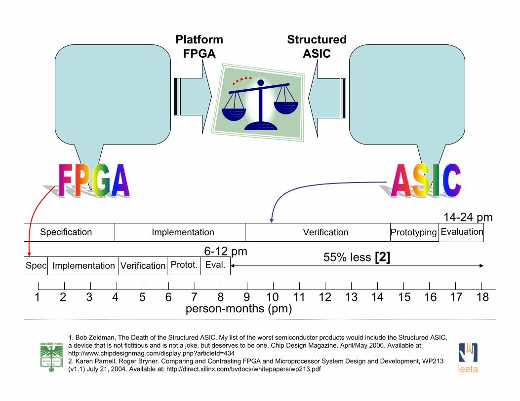
PlatformFPGA
StructuredASIC
1 2 3 4 5 6 7 8 9 10 11 12 13 14 15 16 17 18person-months (pm)
55% less [2]
Specification Implementation Verification Prototyping Evaluation14-24 pm
Spec Implementation Verification Protot. Eval.6-12 pm

Malachy Devlin. Multi-FPGA systems for High Performance Computing applications Available at:http://www.iee.org/oncomms/sector/electronics/Articles/Object/23057E18-0825-84BD-6C1F87BD5B887FF9Malachy Devlin, Reconfigurable Computing Architectures for High Performance Analysis. Available at:http://conferences.iee.org/medsip/Presentations/day1/Medsip-Reconfigurable-Computing-Architectures.pdf
0
200
400
600
800
1000
1200
1400
1600
Clock - MHz
Itanium-2Virtex 2VP100
0
20
40
60
80
100
120
140
P o wer co nsumptio n- Watt
0
5
10
15
20
25
30
35
40
Peak performance -GFLOPs
Sustainedperformance - GFLOPs

Malachy Devlin, Reconfigurable Computing Architectures for High Performance Analysis. Available at:http://conferences.iee.org/medsip/Presentations/day1/Medsip-Reconfigurable-Computing-Architectures.pdf
FPGAs [1]:Can be seen as ‘Soft’ ASICs;Introduce a new computing paradigm;Eliminate the necessity for von Neumann architecture although such architecture can be used if required; Enable the designers to implement algorithms directly in silicon;Make parallelism a key feature;Permit any required external interface to be established, etc.

(When) will FPGAs kill ASICs?The 38th conference on Design automation (2001)
Will Power Kill FPGAs? FPGA 2006 Panel
Did FPGAs kill Structured ASICs? [3]
1. Available at: http://ieeexplore.ieee.org/iel5/7445/20239/00935528.pdf2. Available at: http://conferences.ece.ubc.ca/isfpga2007/www/2006/panel.html3. Available at: http://www.edn.com/blog/1690000169/post/1430004743.html4. Available at: http://pd.pennnet.com/display_article/275920/21/ARTCL/none/none/Programmable_SoCs-_the_end_of_ASICs?/
Programmable SoCs- the end of ASICs? [4]
“FPGA have grown to become multi-million gate devices with system-level features that can implement complete system on a chip. More and more ASIC designers are using FPGAs while the number of designs moving from FPGAs to ASICs is reducing simultaneously”
“ASICs are already dead; they just don’t know it yet”
“Power consumption is now a limitation in many FPGA user applications”

1. SoC Article Series. Available at: http://www.ibm.com/developerworks/views/power/libraryview.jsp?search_by=SoC+drawer:&ca=dgr-wikiaSoCSeries)2. Embedded Processor and System-on-Chip Quick Reference Guide (http://www.linuxdevices.com/articles/AT4313418436.html)3. Luca Benini, Giovanni De Micheli, Networks on Chips: A New SoC Paradigm. Computer, January, 2002.4. John Donovan, Programmable SoCs- the end of ASICs? October, 2006. Available at: http://pd.pennnet.com/display_article/275920/21/ARTCL/none/none/Programmable_SoCs-_the_end_of_ASICs?/
System-on-a-chip (SoC) is a single microchip integrating components for a complex electronic device with typical applications in the scope of embedded systems, telecommunications, multimedia and consumer electronics
SoC includes such components as:• Microcontroller(s), microprocessor(s), DSP(s);• Memory;• Industry standard digital interfaces;• Analog interfaces;• Etc.

The Network on Chip (NoC) employs networking method for communication between sub-systems available on a chip and makes significant improvements over bus systems
To meet the communication requirements of large SoCs, a network-on-chip (NoC) paradigm is emerging as a new design methodology [1].
1. Partha Pratim Pande, Giovanni De Micheli, Cristian Grecu, André Ivanov, and Resve Saleh. Design, Synthesis, and Test of Networks on Chips. IEEE Design and Test of Computers, Volume 22, Issue 5, Sept.-Oct. 2005 pp. 404 – 413.
FPGAs can be seen as a very adequate and promising base for programmable SoCs and NoCs, because of the following:
• Platform FPGAs contain the majority of the required SoC/NoC components;
• Multi-platform FPGAs can be retargeted to the desired scope of SoC/NoC, such as embedded systems, telecommunications, multimedia, etc.;
• FPGA-based design has numerous advantages over other known design techniques.

Reconfigurable Computing [1]“A methodology of using programmable logic devices in a system design such that the hardware-based logic can be changed to perform various tasks”
1. Glossary of Terms. Available at: http://www.xilinx.com/company/terms.htm2. Wikipedia. Reconfigurable computing. Available at: http://en.wikipedia.org/wiki/Reconfigurable_computing3. G. Estrin , Organization of Computer Systems – The Fixed Plus Variable Structure Computer”. Proc. Western Joint
Computer Conf., New York, 1960, pp. 33-40.
Reconfigurable computing [2] “is computer processing with highly flexible computing fabrics. The principal difference whencompared to using ordinary microprocessors is the ability to make substantial changes to the data path itself in addition to the control flow”.
The world's first commercial reconfigurable computer, the Algotronix CHS2X4, was completed in 1991 [2].
The earliest work on reconfigurable computer architecture was done at the University of California at Los Angeles (UCLA) [3].

“The reconfigurable system concept enables different standards and protocols tobe tried, tested, and put on road trials; and if you don’t find them to be suitable, youcan just load in another bus interface and try it out until you find the best” [1]
Reconfigurable system is a system based on reprogrammable logic devices allowing to implement different functionality within the scope of predefined constraints
“A solution that designers are turning to is reconfigurable systems based on FPGAs that can be reprogrammed to accommodate changing standards and protocols late in the design process and even in production” [1]
1. Karen Parnell, Roger Bryner. Comparing and Contrasting FPGA and Microprocessor System Design and Development, WP213 (v1.1) July 21, 2004. Available at: http://direct.xilinx.com/bvdocs/whitepapers/wp213.pdf


• Molecular electronics;• Static and dynamic reconfiguration;• Design flow;• Applications in mobile computing and
multimedia;• Future of reconfigurable systems.

Transistor density of integrated circuits, with respect to minimTransistor density of integrated circuits, with respect to minimal al component cost, doubles every two years component cost, doubles every two years
1000
10000
100000
1000000
10000000
100000000
1000000000
1970
1972
1978
1985
1993
1999
2003
2006
40048008
8080
8086
IntelI286Intel386TM
Intel486TMIntelRPentiumR
IntelRPentiumR II IntelRPentiumR III
IntelRPentiumR 4
IntelRItaniumR IntelRItaniumR 2
IntelRItaniumR 2 (9MB cache)
Data from Intel

-- extends Moore’s Law to other technologiesextends Moore’s Law to other technologies
This file is licensed under Creative Commons Attribution 1.0 License
Kurzweil projects that a continuation of Moore's Law until
2019 will result in transistor features just a few atoms in width
Then, a new type of technology will replace curent integrated
circuit technology
“Moore’s Law cannot continue unabated for more than 600600 years for any technological civilization” 1
1 L.M. Krauss, G.D. Starkman, “Universal Limits of Computation”, http://arxiv.org/abs/astro-ph/0404510&e=10129

Short term: “enhanced CMOS” – heterogeneous integration of new technologies with the CMOS platform
Long term: Inventing fundamentally new approaches to information and signal processing
International Technology Roadmap for Semiconductors, International Technology Roadmap for Semiconductors, Emerging Research DevicesEmerging Research Devices

1D structures (carbon nanotubes, nanowires)
Resonant tunneling devices
SET
Ferromagnetic logic
Spin transistor
Molecular0
50
100
150
200
250
1D RTD SET FL ST M
1Data from ITRS’2005
Number of articles in technical journals that appeared in the Science Citation Index database for July 2003 – July 20051

“The concept of molecular electronicmolecular electronic devices is based on electronic properties of individual molecules tailored to perform logic operations and on the assembly of a large number of these functional building blocks into molecular circuits.” 1
1 International Technology Roadmap for Semiconductors, 2005, Emerging Research Devices
“Organic molecules exist which have two mechanically distinct parts, such as a ring and a rod or interlocking rings. Applying a programming voltage across the molecule adds or subtracts an electron, shifting the ring and changing the molecule’s conductivity. It functions as a non-volatile programmable molecular switch.” 2
2 M. Butts, A. DeHon, S.C. Goldstein, “Molecular Electronics: Devices, Systems and Tools for Gigagate, Gigabit Chips”, ICCAD’2002
“Molecular switches have no gain, so signals must be restored between switch array by devices with gain, such as CNW-FETs.” 2

“Carbon nanotube is a molecular sheet a single atom thick, which has wrapped around into a tube, as little as one nanometer wide” 1
1 M. Butts, A. DeHon, S.C. Goldstein, “Molecular Electronics: Devices, Systems and Tools for Gigagate, Gigabit Chips”, ICCAD’2002
“Nanowires can be grown to hundreds of microns or perhaps millimeters in length. However, at this high length to diameter ratio, they become highly susceptible to bending and ultimately breaking.” 2
2 A. DeHon, “Nanowire-Based Programmable Architectures”, ACM Journal on Emerging Technologies in Computing Systems, Vol. 1, No. 2, July 2005.
Arrays of modest-size crossed nanowires with switchable diodes at crosspoints can be used for constructing memory cores and programmable crossbar interconnect arrays.
Each NW has to be addresses uniquely in order to program individual crosspoints allowing to implement a given logic function and routing and to avoid defective NW.

In current technologies, FPGA area is greatly determined by the area of its programmable switches.
Molecular-scale programmable switches are estimated to be two orders of magnitude smaller than lithographic crosspoints.
Although molecular FPGA will have overhead for lithographic support and defect tolerance, it is expected that molecular FPGA will surpass lithographic CMOS ASICs in density in the early 2010s. 1
1 M. Butts, A. DeHon, S.C. Goldstein, “Molecular Electronics: Devices, Systems and Tools for Gigagate, Gigabit Chips”, ICCAD’2002
It was shown that fully programmable, post-fabrication configurable, FPGA can be built with all logic and restoration occurring at the nanoscale.

Very high device densities may be achieved;
Switching energy may be significantly reduced (comparing to CMOS) and may approach the thermodynamic limit;
The speed of molecular devices is limited and is expected to be much lower than that of CMOS;
Novel architectures will have to be more defect-tolerant relative to current CMOS devices;
Since FPGA are based on very regular crossbar structures they “offer the best chance for eventually fabricating nanocomputers with more than 1010
devices on a chip.” 1
Cost per gate in molecular devices is estimated to be much lower than for any other kind of device in the year 2016 (varying from $1E-12 to $1E-10 1).
1 International Technology Roadmap for Semiconductors, 2005, Emerging Research Devices

StaticStatic
Probleminstance Configuration Execution Result
Probleminstance
(modify)configuration Execution Result
DynamicDynamic• global • partial

Application Configuration

Application
A
B
C

Application
Main configuration
A B C

new configuration
new configuration
new configuration

- Ability to reconfigure selected FPGA areas anytime after its initial configuration
ActiveActive partial reconfiguration – reconfiguration is done while the design is operational and the device is active
StaticStatic partial reconfiguration – reconfiguration is done while the device is inactive
Advantages of partial reconfiguration:Advantages of partial reconfiguration:
Adaptability of hardware algorithms;
Ability to share hardware between applications;
Increased resource utilization, reduced device count, power consumption and overall costs;
Shorter reconfiguration times;
Ability to provide continuous hardware servicing;
Possibility to upgrade hardware remotely.

Examples: VirtexVirtexTMTM--44, SpartanSpartanTMTM--3/E3/E
Difference-based partial reconfiguration allows small changes to be made in an FPGA design and then bitstream is generated based on only the differences in the two designs.
Module-based partial reconfiguration uses modular design concepts to reconfigure large blocks of logic
Fixedlogic
Rec
onfig
urab
lem
odul
e
Rec
onfig
urab
lem
odul
e
Fixedlogic
Fixedlogic
Fixedlogic
BUS
MACRO
BUS
MACRO
BUS
MACRO

SpecificationSpecification
VerificationVerification
ImplementationImplementation
FPGA
SynthesisSynthesis
behavioralsimulation
functionalsimulation
timingsimulation
in-circuitverification

Schematic entryHardware description languagesSystem-level specification languagesGeneral-purpose languages
SpecificationSpecification
VerificationVerification
ImplementationImplementation
FPGA
SynthesisSynthesis

Celoxica DK Design Suite 1
Specificationin Handel-C
EDIFfile
Xilinx ISE 2
1 http://www.celoxica.com2 http://www.xilinx.com
Specificationin VHDL
XST
Implementation
SpecificationSpecification
VerificationVerification
ImplementationImplementation
FPGA
SynthesisSynthesis

Specificationin standard C/C++
1 http://www.celoxica.com2 http://www.xilinx.com
SpecificationSpecification
VerificationVerification
ImplementationImplementation
FPGA
SynthesisSynthesis
Algorithm simulation
Software/Hardware
partitioning
Export toimplementation
tools
Generate synthesizable
HDL code
Generate Software/Hardware
interfaces

Accelchip provides high-level FPGA design tools based on Matlab and Simulink. Agilent provides an effective solution for in-circuit debug of FPGA and surrounding systems. Aldec provides FPGA design and verification tools, including a popular HDL simulator. Altera provides FPGA design, sinthesis, implementation and verification tools.Altium provides FPGA synthesis and simulation tools, as well as royalty-free IP blocks that include processor cores. Annapolis Micro Systems, Inc. provides the CoreFire Design Suite for high-level design entry, and IP blocks for digital signal processing. Celoxica provides Handel-C tools for high-level design entry and verification. Gedae provides high-level FPGA and DSP programming tools allowing programmers to develop to hetergenous systems and related optimization and verification tools. Impulse provides the Impulse C compiler and related optimization and verification tools. LogicSim provides a free Windows-based Verilog simulator and debugger, useful for FPGA RTL verification. Lyrtech provides hardware combining FPGA and DSP technologies plus high-level FPGA-DSP design tools based on Matlab, Simulink, Xilinx Sysgen and Texas Instruments CCS. MathWorks provides Simulink, a tool that is used as a high level design entry for FPGAs. Mentor provides the Catapult C high-level design tools, as well as a wide range of HDL synthesis andsimulation tools. National Instruments provides FPGA development boards and LabVIEW FPGA, a high level graphical programming language with built-in IP blocks Synopsys provides HDL synthesis tools, as well as a broad range of verification and high-level design tools. Synplicity provides HDL synthesis, FPGA physical synthesis and verification tools. Xilinx provides HDL design, synthesis, implementation and in-circuit verification tools.
... not complete!... not complete!

0
0,5
1
1,5
2
2,5
3pe
rfor
man
ce
reso
urce
usag
e
porta
bilit
y
ease
to le
arn
ease
toch
ange
and
mai
ntai
nanc
e
deve
lopm
ent
time
SchematicHDLSLSLGPPL
“The days of designing FPGAs with schematics are gone.” 1
1 R. Goering, “FPGA users rank challenges, tasks”, EE Times, 07/31/2006

Chi
p co
mpl
exity
(lo
g sc
ale)
Time
Moore’s Law
Des
ign
prod
uctiv
ity(lo
g sc
ale)
Design productivity is a real challenge for future systemsDesign productivity is a real challenge for future systems
PlatformFPGA
PlatformPlatformFPGAFPGA
-- inherited from ASICinherited from ASIC
Design productivity

Reuse intellectual property (IP) to improve design productivity
1 International Technology Roadmap for Semiconductors, 2005
– design effort for the reused logic is only a portion of the effort needed for newly designed logic– reuse rate for system-level design is expected to increase from 32% in 2005 to
55% in 2020 1
Design abstraction levels must be raised
The level of automation must be increased
– further improvement in design tools
– automated HW/SW partitioning in high-level design stages
– “higher levels of abstraction allow many forms of verification to be performed much earlier in the design process, reducing time to market and lowering cost” 1
– reduce the number of iterations

Mobile and multimedia applications became an important driver foMobile and multimedia applications became an important driver for r FPGA products and technologiesFPGA products and technologies
The life cycle of mobile consumer products is short, and will stay short in the future. Therefore, the design effort cannot be increased - it needs to stay at the current level for the foreseeable future. 1
1 International Technology Roadmap for Semiconductors, 2005, System Drivers
Portable devices are highly power-dependant
Autonomous mobile devices used in applications (such as medical, space), where repair by human experts is for some reason impossible, may require to be either autonomously or remotely repaired
New design techniques: evolvable hardware – possibility to construct a circuit with a given specification, whose structure is previously unknown
– need to shorten time to market and to lower system costs (NRE, design and test)
– need to optimize processing per microwatt
– need for (remote) reconfigurability and adaptability, and also for simplifying recertification and preventing obsolescence issues
– need for self-reconfigurability

1 M. Uhm, “Making the Adaptivity of SDR and Cognitive Radio Affordable”, DSP Magazine, May 2006
-- Software defined radios and cognitive radios Software defined radios and cognitive radios 11
Feature demanded: adaptabilityadaptability- to spectral environment;- a waveform to compensate for channel fading;- collaborate with multiple radios to receive a weak signal;- accommodate damage to some of a radio’s processing resources byreconfiguring the remaining resources to support the most critical services;
- etc.
Partially reconfigurable platform FPGA have high processing throughput and can provide different levels of adaptability at low power and cost.
Service(radio services, anti-jam services)
Application(waveforms)
Component(digital converters)
Functional(filters, transforms)

1 M. Devlin, “Multi-FPGA systems for High Performance Computing applications”, IEE Developers Forum, October 2005
-- Algorithm acceleration in NallatechAlgorithm acceleration in Nallatech1,21,2
Seismic processing - Kirchhoff algorithm- calculations in IEEE 754- 64 times faster than a 2GHz Pentium 4- 200 times less power consumption
Biological sequencingReal-time video processingGravity simulation
2 “R. Associates Joins Nallatech’s Growing Channel Partner Program”, FPGA and Structured ASIC Journal, August 2005
“The FPGA solution saves more than $10,000 in electricity bills per year per 64-processor 19’’ rack, based on seven cents per kilowatt hour”2
Remote mobile computing for gas and oil exploration Remote mobile computing for gas and oil exploration ((Nallatech’sNallatech’s work with R. Associates)work with R. Associates) 22
performance improvement
reduced space

1 S. Margerm, “Reconfigurable Computing in Real-World Applications”, FPGA and Structured ASIC Journal, February 2006
-- Biotech applicationsBiotech applications
SmithSmith--Waterman algorithmWaterman algorithm – a life sciences application for comparing DNA and amino acid sequences against known genes and proteins 1
scoringmatrix
calculation
code
scoringmatrix
calculation(98 %)
time
scoringmatrix
calculation(98 %)
Cray XD1 2
64×
2 http://www.cray.com
FPGA(Xilinx Virtex-4)
FPGA(Xilinx Virtex-4)
CPU(AMD Opteron)
CPU(AMD Opteron)
CacheCache
high-speed I/O
RapidArray interconnect

1 http://www.sundance.com/
-- Image processingImage processing
- color space conversion;- transforms (DCT, FFT);- convolution;
Sundance image processing development platforms 1
- interactive gaming;- medical image scanning;- security systems (iris scanning, automatic number plate recognition);- etc.
Virtex-4FPGA
CoolRunner IICPLD
ZBTRAM2×2M×18
I/O
Clocking scheme
Flash PROM2×2M×18

-- Automotive infotainment Automotive infotainment 11
FPGAFPGAspeakers
TFT LCD
DVD
radio
graphicsacceleration
audioprocessing
filtering and formatting
CANcontroller
TFT timing
discretelogic
- reduced system cost;- low power;- increased flexibility.
1 M. Dickinson, “Tools for System Level Design”, Altera, 2005http://www.iee.org/oncomms/sector/electronics/Articles/Object/2301030F-AEFC-4F99-12D5DA60F20AA683

-- Speech enhancement Speech enhancement 11
- speech recognition systems;- surveillance;
1 D. Halupka, “FPGA-Based Speech Enhancement”, University of Toronto, October 2005http://www.iee.org/oncomms/sector/electronics/Articles/Object/13A61100-C5E8-B3D0-FDD78B36C6E2A0C6
GPP DSP FPGA (Cyclone 12 K)
ASIC
Design time 1-2 weeks 3-4 weeks 2-3 months over a year Power consumption
23 – 100 W 350 mW 183 mW 3.45 mW
Performance not real-time barely real-time real-time real-time

-- FunctionsFunctions
- searching;- sorting;- coding/decoding;- signal processing;- audio/video/image manipulation;- encryption;- error correction;- random number generation;- packet processing;- recovery from SEU;- etc.
- seismic processing;- acoustics;- astrophysics FFT;- adaptive optics;- cryptography;- graphics acceleration;- HDTV;- mobile radio;- car multimedia systems;- image recognition;- speech recognition;- security;- video format translation;- biotech applications;- vehicular traffic simulation;- financial modeling;- orbit, space, and extra-terrestrial applications
- etc.
-- ApplicationsApplications
Real-timeReal-time

0
10
20
30
40
50
60
70
Aerospace Video Military Automotive Networking Government Security
1 J. Turley, “Survey: Who uses custom chips”, Embedded Systems Design, 08/01/2005
41%41% of developers overall are using one or more FPGA in their projects 1
35%35% of developers overall do not use any custom logic in their projects 1

1 International Technology Roadmap for Semiconductors, 2005, Design
“The growing system complexity will make it impossible to ship designs without errors in the future. Hence, it is essential to be able to fix errors after fabrication. In addition, reconfigurability increases reuse, since existing devices can be reprogrammed to fulfill new tasks.” 1
0
10
20
30
40
50
60
70
2005 2006 2007 2008 2009 2010 2011 2012 2013 2014 2015 2016 2017 2018 2019 2020
% o
f SO
C fu
nctio
nally
reco
nfig
urab
le

Peripherals
PEPEPEPEPEPE
PEPEPEPEPEPE
PEPEPEPEPEPE
PEPEPEPEPEPE
PEPEPEPEPEPE
PEPEPEPEPEPEMain
processor
Mainmemory
High processing performanceHigh processing performance Low power consumptionLow power consumption

The number of PE will grow exponentially 1
0
100
200
300
400
500
600
700
800
900
2005 2006 2007 2008 2009 2010 2011 2012 2013 2014 2015 2016 2017 2018 2019 2020
# of
PE
1 International Technology Roadmap for Semiconductors, 2005, System Drivers

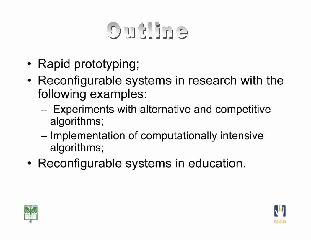
• Rapid prototyping;• Reconfigurable systems in research with the
following examples:– Experiments with alternative and competitive
algorithms;– Implementation of computationally intensive
algorithms;• Reconfigurable systems in education.

There are many prototyping boards available for engineering and research (see, for example, [1])
Experience with the following prototyping boards (systems):
Annapolis FireFlyTM (FPGA XC6216/6264) - 1997-2001;XESS XS40 (FPGA XC4010XL) - 1998-2002;Alpha Data ADM-XRC (FPGA Virtex-EM XCV812E) - 2000-2003;Alpha Data ADM-XPL (FPGA Virtex-II Pro XC2VP7) - from 2003;XESS XSA100 (FPGA Spartan-II XC2S100) - from 2002;Trenz TE-XC2Se (FPGAs Spartan-IIE XC2S300E/400E) - from 2002;Celoxica RC100 (FPGA Spartan-II XC2S200) - from 2002;Celoxica RC200 (FPGA Virtex-II XC2V1000) - from 2003;Celoxica RC10 (FPGA Spartan-3 XC3S1500L) - from 2005;DETIUA-S3 (FPGA Spartan-3 XC3S400 ) - from 2005.
1. Xilinx prototyping board list. Available at: http://www.xilinx.com/ Development boards
Designed at the department by Manuel AlmeidaSoftware was designed by Bruno Pimentel

Interfacesocket
Hardware designed by Manuel Almeida.
Software designed by Bruno Pimentel.

Bitstream for configurationFirst logical section
User bitstreamSecond logical section
User data / alternative bitstreams
Third logical section
Hardware designed by Manuel AlmeidaSoftware designed by Bruno Pimentel

USB module
Bluetooth module
Hardware designed by Manuel AlmeidaSoftware designed by Bruno PimentelPeripheral projects designed by the authors and students

interface with PC
USB module
Extension hardware forinteractions with sensors
and actuators
Simulation of an executionunit in virtual mode on PC
monitor screen
Hardware designed by Manuel AlmeidaSoftware designed by Bruno PimentelSimulation software designed by students
Ext
ensi
on h
ardw
are
for
inte
ract
ions
with
sen
sors
and
actu
ator
s

Extensions fordifferent
interfaces
Using devices designed by students
etc.

Bluetooth module
Embeddedcontroller
Wirelesscommunication
Bluetooth module
Embeddedcontroller
Wirelesscommunication
Hardware designed by Manuel AlmeidaSoftware designed by Bruno Pimentel

1) 172) 63) 184) 95) 56) 217) …
17root of a binary tree
6
left node because 6 < 17
right node because 18 > 17
18
9
right node ofthe node 6, because
9 < 17 and 9 > 6
5
left node ofthe node 6, because
5 < 17 and 5 < 6
21
right node ofthe node 18, because21 > 17 and 21 > 18

// Function template to create a root node or add a nodetemplate<class T> treenode<T> *addnode(treenode<T> *node, T value) {if(node==0) {
// constructing a new node of type treenode<T>node = new treenode<T>; // exception handlingnode->val = value; // Store new value in nodenode->count = 1; // Only one to start. At thenode->rnode = node->lnode = 0; // beginning we have just one node
} else if(value==node->val)node->count++; // increment the counter
else if(value < node->val)// traverse the tree or construct the left nodenode->lnode = addnode(node->lnode,value);
else// traverse the tree or construct the right nodenode->rnode = addnode(node->rnode,value);
return node; // return a pointer to the current node }
17
6 18
95

It is known that recursion is an extremely powerful problem-solving technique that permits a problem to be decomposed into smaller sub-problems that are of exactly the same form as the original problem
However this technique is not always appropriate, particularly when a clear efficient iterative solution exists
This is primarily due to the large amount of states that are accumulated during deep recursive calls
Besides in most high-level programming languages, a function call incurs a bookkeeping overhead. Recursive functions magnify this overhead because a single initial call to the function might generate a large number of recursive invocations of the function

// Function template to sort and output a treetemplate<class T> void treesort(treenode<T> *node) {if(node!=0) // if the node exists{ treesort(node->lnode); // Sort left sub-tree
// Display value after any hierarchical returncout << "value - " << node->val << "; repeated - " << node->count << endl;treesort(node->rnode); // Now sort right sub-tree
}}
Begin
x1
y3
0
1
a0
a1
a2
End, y5
a3
a4
y1,y2,z2
y1,y4,z2
Z2

17
6 18
3 12
10 15
13
14
Begin
x1
y3
0
1
a0
a1
a2
End, y5
a3
a4
y1,y2,z2
y1,y4,z2
Z2
avoid

17
6 18
3 12
10 15
13
14
Recursive calls
(recursive) returns
z2
Begin
x6
x7
y1,y2,zz22
y3
y1,y4,zz22
End, y5
1
1
0
0

z2
Begin
x6
x7
y1,y2,zz22
y3
y1,y4,zz22
End, y5
1
1
0
0
z1
Begin
x3
x1
x2
x4
y1,y2,zz11 y9y1,y4,zz11 y6,y8 y7,y8
End, y10
10
1 0
1 0
1 0
Begin
zz22
End
0
zz11
x5
1z0

X2
X4
Begin
y9
1
00
x6 x7
10
y2
y6,y8 y4y7,y8
1
0
0
1
X30
1
y10
xx21
x7
0
1
x6
y2
0
1y3
y4
End0
xx11
0
y1,y5
X10
1
sorting
construction of the tree

• Iterative implementation:– VHDL: (using Finite State Machines - FSM);– Handel-C: (using constructions similar to C language).
• Recursive and Modular implementation:– VHDL: (using Hierarchical Finite State Machines - HFSM);– Handel-C: (using Hierarchical Finite State Machines -
HFSM).

Implemented algorithms for:
– (P1) Sorting• based on a binary tree (tree-based)
– (P2) finding a minimal row cover of a binary matrix• 128x128 matrices; approximate method (cyclic)
– (P3) the Knapsack problem• exact binary search method (tree-based)
– (P4) GCD computation• GCD of 2 unsigned integers (cyclic)
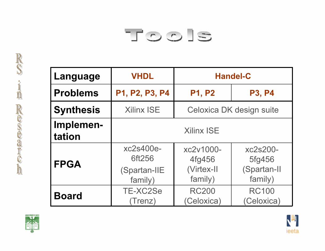
RC100 (Celoxica)
RC200 (Celoxica)
TE-XC2Se (Trenz)Board
xc2s200-5fg456
(Spartan-II family)
xc2v1000-4fg456
(Virtex-II family)
xc2s400e-6ft256
(Spartan-IIE family)
FPGA
Xilinx ISEImplemen-tation
Celoxica DK design suiteXilinx ISESynthesis
P3, P4P1, P2P1, P2, P3, P4Problems
Handel-CVHDLLanguage

Number of Slices of Recursive implementation
Number of Slices of Iterative implementation
Execution Time of Recursive implementation
Execution Time of Iterative implementation
Legend:
0
100
200
300
400
500
600
700
P1 P1/MI P1/MI/BM P1/MI/DM
Numberof Slices
0
500
1,000
1,500
2,000
2,500
ExecutionTime (ns)
140
145
150
155
160
165
170
P3 P3/MI P3/MI/BM P3/MI/DM
Numberof Slices
1,300
1,350
1,400
1,450
1,500
1,550
1,600
1,650
1,700
ExecutionTime (ns)
400
420
440
460
480
500
520
540
P4 P4/MI P4/MI/BM P4/MI/DM
Numberof Slices
0
50
100
150
200
250
300
ExecutionTime (ns)
P1 – Sorting (tree-based)
P3 – Knapsack (tree-based) P4 – GCD (cyclic)

0
1,000
2,000
3,000
4,000
5,000
6,000
Numberof Slices
0
1,000,000
2,000,000
3,000,000
4,000,000
5,000,000
6,000,000
7,000,000
8,000,000
ExecutionTime (ns)
0
200
400
600
800
1,000
1,200
1,400
Numberof Slices
0
500
1,000
1,500
2,000
2,500
ExecutionTime (ns)
0
100
200
300
400
500
600
700
Numberof Slices
0
2,000
4,000
6,000
8,000
10,000
12,000
14,000
ExecutionTime (ns)
0
50
100
150
200
250
300
Numberof Slices
0
50
100
150
200
250
300
350
400
ExecutionTime (ns)
P2 – Minimal Row Cover (cyclic)P1 – Sorting (tree-based)
P3 – Knapsack (tree-based) P4 – GCD (cyclic)

• Recursion can be implemented in hardware much more efficiently than in software;
• This is because any activation of a recursive subsequence of operations has been combined with the execution of the operations that are required by the respective algorithm. The same event takes place when any recursive sub-sequence is being terminated, i.e. when control has to be returned to the point after the last recursive call and an operation of the executing algorithm that follows the last recursive call has to be activated;
• The number of states required for the execution of a recursion in hardware can be reduced significantly compared with software but it is still greater than for iterative solutions;
• However such states are accumulated on stacks typically implemented on built-in memory blocks, which are relatively cheap;
• C/C++ implementations of iterative algorithms are faster comparing with recursive algorithms;
• VHDL-based projects for recursive algorithms give better results (resources and execution time) comparing with iterative algorithms;
• Handel-C based projects for iterative algorithms give better or similar results (resources and execution time) comparing with recursive algorithms.

111111111111111111111101100101110100010100001111111011010001001001110101100010001100001011110010110101011100
987654321
lkjihgfedcba
1
1
1
1
1
1
1
1
1
Discrete matrix can be seen as a very
adequate model for solving combinatorial problems in hardware.

=
101100000111111001001101110100011010
765432
M
lhgcba
=
0011111100
63
M
lhcba
=
111000011101101
764
M
lgcba
Applying reduction rules:delete rows 8,9; columns d, e, f, i, j, row 1; column k
column b
Applying reduction rules:delete columns a, h; row 7
column c
{b, c, l}
column l
[ ]15Ml
=
{b, l, ...}
column g
Applying reduction rules:delete columns a,b,h,l;
=
10110111010011111010
7543
M
lhgca
=
110011101
543
M
lgc
=
11
63
M
c
{c, g}
column h
delete rows 2,3,5; column hdelete rows 2,6; column b delete rows 2,4,5,7; column g
{h, ...}
[ ]114Mgc
=stop
stop
The decision tree is constructed during the search process and it is traversed starting from the root

A B C D E F G1 1 - - 1 - - -2 1 - - 0 - 1 -3 1 - - 1 - - 04 1 - - - - 0 -5 0 - 0 - 1 - -6 0 - 0 - 0 - -7 0 - 1 1 1 - 18 0 - 1 - 0 0 -
;
A B C D E F G0 - 1 0 - 1 -

General Purpose Computer FPGA
Data compressionin software ( TS )
Data decompressionin hardware ( Rh, Th )
Software partfor SAT solver
Hardware partfor SAT solver
Transmittingnon-compressed
result
Transmittingcompressed
data ( Tt )

1 2 3 4 5
6 7 8 9 10

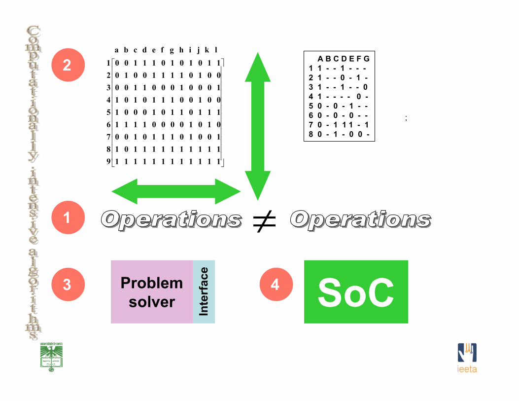
• Combinatorial search algorithms have two following distinctive features:They require a huge number of different variants (feasible solutions) to be considered;These variants can be ordered and examined with the aid of a decision tree that provides an efficient way for handling intermediate solutions.
• The decision tree is constructed during the search process and it is traversed starting from the root.
• Many combinatorial algorithms have to deal with a huge amount of data, which have to be transferred between a host computer and an FPGA-based accelerator. In many circumstances, due to the complexity, the problem cannot be completely solved just in an FPGA, and combined hardware/software solutions are employed. This involves multiple time consuming data transfers. To simplify the problem compression/ decompression technique can be used.
111111111111111111111101100101110100010100001111111011010001001001110101100010001100001011110010110101011100
987654321
lkjihgfedcba
A B C D E F G
1 1 - - 1 - - -2 1 - - 0 - 1 -3 1 - - 1 - - 04 1 - - - - 0 -5 0 - 0 - 1 - -6 0 - 0 - 0 - -7 0 - 1 1 1 - 18 0 - 1 - 0 0 -
;
≠Problemsolver
Inte
rfac
e
SoC
1
2
3 4
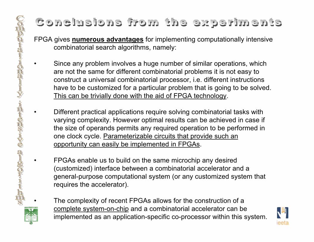
FPGA gives numerous advantages for implementing computationally intensive combinatorial search algorithms, namely:
• Since any problem involves a huge number of similar operations, which are not the same for different combinatorial problems it is not easy to construct a universal combinatorial processor, i.e. different instructions have to be customized for a particular problem that is going to be solved. This can be trivially done with the aid of FPGA technology.
• Different practical applications require solving combinatorial tasks with varying complexity. However optimal results can be achieved in case if the size of operands permits any required operation to be performed in one clock cycle. Parameterizable circuits that provide such an opportunity can easily be implemented in FPGAs.
• FPGAs enable us to build on the same microchip any desired (customized) interface between a combinatorial accelerator and ageneral-purpose computational system (or any customized system that requires the accelerator).
• The complexity of recent FPGAs allows for the construction of a complete system-on-chip and a combinatorial accelerator can be implemented as an application-specific co-processor within this system.


• FPGAs have proven their effectiveness in research and development.
• FPGA market is rapidly expanding its boundaries and this tendency will be kept in future.
• Available design tools allow for fast creation of highly optimized systems in vast varieties of application areas and at different levels of abstraction.
• The progress in FPGA technology is not sufficiently covered by the majority of university curricula.