ts 151 021 - v9.6.0 - digital cellular telecommunications ... · 3gpp ts 51.021 version 9.6.0...
TRANSCRIPT

ETSI TS 151 021 V9.6.0 (2011-06)
Technical Specification
Digital cellular telecommunications system (Phase 2+);Base Station System (BSS) equipment specification;
Radio aspects (3GPP TS 51.021 version 9.6.0 Release 9)
GLOBAL SYSTEM FOR MOBILE COMMUNICATIONS
R
ETSI
ETSI TS 151 021 V9.6.0 (2011-06)13GPP TS 51.021 version 9.6.0 Release 9
Reference RTS/TSGG-0151021v960
Keywords GSM
ETSI
650 Route des Lucioles F-06921 Sophia Antipolis Cedex - FRANCE
Tel.: +33 4 92 94 42 00 Fax: +33 4 93 65 47 16
Siret N° 348 623 562 00017 - NAF 742 C
Association à but non lucratif enregistrée à la Sous-Préfecture de Grasse (06) N° 7803/88
Important notice
Individual copies of the present document can be downloaded from: http://www.etsi.org
The present document may be made available in more than one electronic version or in print. In any case of existing or perceived difference in contents between such versions, the reference version is the Portable Document Format (PDF).
In case of dispute, the reference shall be the printing on ETSI printers of the PDF version kept on a specific network drive within ETSI Secretariat.
Users of the present document should be aware that the document may be subject to revision or change of status. Information on the current status of this and other ETSI documents is available at
http://portal.etsi.org/tb/status/status.asp
If you find errors in the present document, please send your comment to one of the following services: http://portal.etsi.org/chaircor/ETSI_support.asp
Copyright Notification
No part may be reproduced except as authorized by written permission. The copyright and the foregoing restriction extend to reproduction in all media.
© European Telecommunications Standards Institute 2011.
All rights reserved.
DECTTM, PLUGTESTSTM, UMTSTM, TIPHONTM, the TIPHON logo and the ETSI logo are Trade Marks of ETSI registered for the benefit of its Members.
3GPPTM is a Trade Mark of ETSI registered for the benefit of its Members and of the 3GPP Organizational Partners. LTE™ is a Trade Mark of ETSI currently being registered
for the benefit of its Members and of the 3GPP Organizational Partners. GSM® and the GSM logo are Trade Marks registered and owned by the GSM Association.

ETSI
ETSI TS 151 021 V9.6.0 (2011-06)23GPP TS 51.021 version 9.6.0 Release 9
Intellectual Property Rights IPRs essential or potentially essential to the present document may have been declared to ETSI. The information pertaining to these essential IPRs, if any, is publicly available for ETSI members and non-members, and can be found in ETSI SR 000 314: "Intellectual Property Rights (IPRs); Essential, or potentially Essential, IPRs notified to ETSI in respect of ETSI standards", which is available from the ETSI Secretariat. Latest updates are available on the ETSI Web server (http://webapp.etsi.org/IPR/home.asp).
Pursuant to the ETSI IPR Policy, no investigation, including IPR searches, has been carried out by ETSI. No guarantee can be given as to the existence of other IPRs not referenced in ETSI SR 000 314 (or the updates on the ETSI Web server) which are, or may be, or may become, essential to the present document.
Foreword This Technical Specification (TS) has been produced by ETSI 3rd Generation Partnership Project (3GPP).
The present document may refer to technical specifications or reports using their 3GPP identities, UMTS identities or GSM identities. These should be interpreted as being references to the corresponding ETSI deliverables.
The cross reference between GSM, UMTS, 3GPP and ETSI identities can be found under http://webapp.etsi.org/key/queryform.asp.

ETSI
ETSI TS 151 021 V9.6.0 (2011-06)33GPP TS 51.021 version 9.6.0 Release 9
Contents
Intellectual Property Rights ................................................................................................................................ 2
Foreword ............................................................................................................................................................. 2
Foreword ............................................................................................................................................................. 9
1 Scope ...................................................................................................................................................... 10
2 References .............................................................................................................................................. 11
3 Definitions, abbreviations, frequency bands and channels..................................................................... 12
3.1 Definitions ........................................................................................................................................................ 12
3.2 Abbreviations ................................................................................................................................................... 14
3.3 Frequency bands and channels ......................................................................................................................... 14
3.3.1 Frequency bands ......................................................................................................................................... 14
3.3.2 Channels and channel numbering ............................................................................................................... 15
4 General test conditions and declarations ................................................................................................ 15
4.1 Output power and determination of power class .............................................................................................. 15
4.2 Specified frequency range ................................................................................................................................ 16
4.3 Frequency hopping ........................................................................................................................................... 16
4.4 RF power control .............................................................................................................................................. 17
4.5 Downlink discontinuous transmission (DTX) .................................................................................................. 17
4.6 Test environments ............................................................................................................................................ 17
4.6.1 Normal test environment ............................................................................................................................ 17
4.6.2 Extreme test environment ........................................................................................................................... 17
4.6.2.1 Extreme temperature ............................................................................................................................. 18
4.6.3 Vibration ..................................................................................................................................................... 18
4.6.4 Power supply .............................................................................................................................................. 18
4.7 Acceptable uncertainty of measurement equipment ......................................................................................... 19
4.8 Interpretation of measurement results .............................................................................................................. 22
4.9 Selection of configurations for testing.............................................................................................................. 23
4.10 BTS Configurations .......................................................................................................................................... 23
4.10.1 Receiver diversity ....................................................................................................................................... 23
4.10.2 Duplexers .................................................................................................................................................... 24
4.10.3 Power supply options .................................................................................................................................. 24
4.10.4 Ancillary RF amplifiers .............................................................................................................................. 24
4.10.5 BSS using antenna arrays ........................................................................................................................... 25
4.10.6 BTS supporting 8-PSK modulation ............................................................................................................ 26
4.10.7 BTS supporting additional modulations in EGPRS2 .................................................................................. 26
4.10.8 Supported Symbol Rate .............................................................................................................................. 27
4.10.9 Support of RTTI and/or FANR .................................................................................................................. 27
4.10.10 Multicarrier BTS ......................................................................................................................................... 27
5 Format and interpretation of tests ........................................................................................................... 28
6 Transmitter ............................................................................................................................................. 29
6.1 Static Layer 1 functions .................................................................................................................................... 29
6.1.1 Test purpose ................................................................................................................................................ 29
6.1.2 Test case ..................................................................................................................................................... 29
6.1.3 Essential conformance ................................................................................................................................ 29
6.1.4 Complete conformance ............................................................................................................................... 29
6.1.5 Requirement reference ................................................................................................................................ 30
6.2 Modulation accuracy ........................................................................................................................................ 30
6.2.1 Test purpose ................................................................................................................................................ 30
6.2.2 Test case ..................................................................................................................................................... 30
6.2.3 Essential conformance ................................................................................................................................ 31
6.2.4 Complete conformance ............................................................................................................................... 32
6.2.5 Requirement reference ................................................................................................................................ 33
6.3 Mean transmitted RF carrier power .................................................................................................................. 33

ETSI
ETSI TS 151 021 V9.6.0 (2011-06)43GPP TS 51.021 version 9.6.0 Release 9
6.3.1 Test purpose ................................................................................................................................................ 33
6.3.2 Test case ..................................................................................................................................................... 33
6.3.3 Essential conformance ................................................................................................................................ 34
6.3.4 Complete conformance ............................................................................................................................... 35
6.3.5 Requirement reference ................................................................................................................................ 35
6.4 Transmitted RF carrier power versus time ....................................................................................................... 35
6.4.1 Test purpose ................................................................................................................................................ 35
6.4.2 Test case ..................................................................................................................................................... 35
6.4.3 Essential conformance ................................................................................................................................ 36
6.4.4 Complete conformance ............................................................................................................................... 36
6.4.5 Requirement reference ................................................................................................................................ 40
6.5 Adjacent channel power ................................................................................................................................... 40
6.5.1 Spectrum due to modulation and wideband noise....................................................................................... 40
6.5.1.1 Test purpose .......................................................................................................................................... 40
6.5.1.2 Test case ................................................................................................................................................ 40
6.5.1.3 Essential Conformance .......................................................................................................................... 41
6.5.1.4 Complete conformance ......................................................................................................................... 43
6.5.1.5 Requirement reference .......................................................................................................................... 44
6.5.2 Switching transients spectrum .................................................................................................................... 44
6.5.2.1 Test purpose .......................................................................................................................................... 44
6.5.2.2 Test case ................................................................................................................................................ 44
6.5.2.3 Essential conformance .......................................................................................................................... 45
6.5.2.4 Complete conformance ......................................................................................................................... 46
6.5.2.5 Requirement reference .......................................................................................................................... 46
6.6 Spurious emissions from the transmitter antenna connector ............................................................................ 46
6.6.1 Conducted spurious emissions from the transmitter antenna connector, inside the BTS transmit band ..... 46
6.6.1.1 Test Purpose .......................................................................................................................................... 46
6.6.1.2 Test Case ............................................................................................................................................... 46
6.6.1.3 Essential conformance .......................................................................................................................... 47
6.6.1.4 Complete conformance ......................................................................................................................... 47
6.6.1.5 Requirement Reference ......................................................................................................................... 47
6.6.2 Conducted spurious emissions from the transmitter antenna connector, outside the BTS transmit band ............................................................................................................................................................ 47
6.6.2.1 Applicability (Phase 2) .......................................................................................................................... 47
6.6.2.1.1 Test Purpose .................................................................................................................................... 47
6.6.2.1.2 Test Case ......................................................................................................................................... 47
6.6.2.1.3 Essential conformance ..................................................................................................................... 48
6.6.2.1.4 Complete conformance .................................................................................................................... 48
6.6.2.1.5 Requirement Reference ................................................................................................................... 49
6.6.2.2 Applicability (Phase 2+) ....................................................................................................................... 49
6.6.2.2.1 Test Purpose .................................................................................................................................... 49
6.6.2.2.2 Test Case ......................................................................................................................................... 49
6.6.2.2.3 Essential conformance ..................................................................................................................... 50
6.6.2.2.4 Complete conformance .................................................................................................................... 51
6.6.2.2.5 Requirement Reference ................................................................................................................... 51
6.6.2.3 Applicability (Release 1999 and later releases GSM 400, GSM 900 and DCS 1800) .......................... 52
6.6.2.3.1 Test Purpose .................................................................................................................................... 52
6.6.2.3.2 Test Case ......................................................................................................................................... 52
6.6.2.3.3 Essential conformance ..................................................................................................................... 53
6.6.2.3.4 Complete conformance .................................................................................................................... 53
6.6.2.3.5 Requirement Reference ................................................................................................................... 53
6.6.2.4 Applicability (Release 4 and later releases GSM 700, GSM 850 and PCS 1900) ................................ 53
6.6.2.4.1 Test Purpose .................................................................................................................................... 53
6.6.2.4.2 Test Case ......................................................................................................................................... 53
6.6.2.4.3 Essential conformance ..................................................................................................................... 54
6.6.2.4.4 Complete conformance .................................................................................................................... 54
6.6.2.4.5 Requirement Reference ................................................................................................................... 54
6.6.2.5 Applicability (Release 7 and later releases GSM 400, T-GSM 810, GSM 900 and DCS 1800) ........... 54
6.6.2.5.1 Test Purpose .................................................................................................................................... 54
6.6.2.5.2 Test Case ......................................................................................................................................... 55
6.6.2.5.3 Essential conformance ..................................................................................................................... 56
6.6.2.5.4 Complete conformance .................................................................................................................... 56

ETSI
ETSI TS 151 021 V9.6.0 (2011-06)53GPP TS 51.021 version 9.6.0 Release 9
6.6.2.5.5 Requirement Reference ................................................................................................................... 57
6.6.2.5a Applicability (Release 7 and later releases GSM 700, GSM 850 and PCS 1900) ................................ 57
6.6.2.5a.1 Test Purpose .................................................................................................................................... 57
6.6.2.5a.2 Test Case ......................................................................................................................................... 57
6.6.2.5a.3 Essential conformance ..................................................................................................................... 58
6.6.2.5a.4 Complete conformance .................................................................................................................... 58
6.6.2.5a.5 Requirement Reference ................................................................................................................... 58
6.6.2.6 Applicability (Release 8 and later releases GSM 400, T-GSM 810, GSM 900 and DCS 1800) ........... 58
6.6.2.6.1 Test Purpose .................................................................................................................................... 58
6.6.2.6.2 Test Case ......................................................................................................................................... 59
6.6.2.6.3 Essential conformance ..................................................................................................................... 60
6.6.2.6.4 Complete conformance .................................................................................................................... 61
6.6.2.6.5 Requirement Reference ................................................................................................................... 62
6.6.2.7 Applicability (Release 8 and later releases GSM 700, GSM 850 and PCS 1900) ................................ 62
6.6.2.7.1 Test Purpose .................................................................................................................................... 62
6.6.2.7.2 Test Case ......................................................................................................................................... 62
6.6.2.7.3 Essential conformance ..................................................................................................................... 63
6.6.2.7.4 Complete conformance .................................................................................................................... 64
6.6.2.7.5 Requirement Reference ................................................................................................................... 65
6.6.2.8 Applicability (Release 8 and later releases GSM 400, GSM 900 and DCS 1800) ................................ 65
6.6.2.8.1 Test Purpose .................................................................................................................................... 65
6.6.2.8.2 Test Case ......................................................................................................................................... 65
6.6.2.8.3 Essential conformance ..................................................................................................................... 66
6.6.2.8.4 Complete conformance .................................................................................................................... 66
6.6.2.8.5 Requirement Reference ................................................................................................................... 66
6.7 Intermodulation attenuation (GSM 400, GSM 900 and DCS 1800) ................................................................ 67
6.7.1 Test purpose ................................................................................................................................................ 67
6.7.2 Test case ..................................................................................................................................................... 67
6.7.3 Essential Conformance ............................................................................................................................... 68
6.7.4 Complete conformance ............................................................................................................................... 69
6.7.5 Requirement reference ................................................................................................................................ 70
6.8 Intra Base Station System intermodulation attenuation .................................................................................... 70
6.8.1 Test purpose ................................................................................................................................................ 70
6.8.2 Test case ..................................................................................................................................................... 70
6.8.3 Essential conformance ................................................................................................................................ 71
6.8.4 Complete conformance ............................................................................................................................... 72
6.8.5 Requirement reference ................................................................................................................................ 72
6.9 Intra Base Station System intermodulation attenuation, MXM 850 and MXM 1900 ...................................... 72
6.9.1 Test purpose ................................................................................................................................................ 72
6.9.2 Test cases .................................................................................................................................................... 72
6.9.2.1 200 kHz carriers-only ............................................................................................................................ 72
6.9.2.2 200 kHz and ANSI-136 30 kHz carriers ............................................................................................... 73
6.9.3 Essential conformance ................................................................................................................................ 73
6.9.4 Complete conformance ............................................................................................................................... 73
6.9.5 Requirement reference ................................................................................................................................ 73
6.10 Intra Base Station System intermodulation attenuation, PCS 1900, GSM 850 and GSM 700 ........................ 74
6.10.1 Test purpose ................................................................................................................................................ 74
6.10.2 Test case ..................................................................................................................................................... 74
6.10.3 Essential conformance ................................................................................................................................ 75
6.10.4 Complete conformance ............................................................................................................................... 75
6.10.5 Requirement reference ................................................................................................................................ 75
6.11 Intermodulation attenuation (GSM 700, GSM 850, MXM 850, PCS 1900 and MXM 1900) ......................... 75
6.11.1 Test purpose ................................................................................................................................................ 75
6.11.2 Test case ..................................................................................................................................................... 75
6.11.3 Essential Conformance ............................................................................................................................... 76
6.11.4 Complete conformance ............................................................................................................................... 78
6.11.5 Requirement reference ................................................................................................................................ 79
6.12 Wideband noise and intra BSS intermodulation attenuation in multicarrier operation .................................... 79
6.12.1 Test purpose ................................................................................................................................................ 79
6.12.2 Test case ..................................................................................................................................................... 79
6.12.3 Essential conformance ................................................................................................................................ 81
6.12.4 Complete conformance ............................................................................................................................... 82

ETSI
ETSI TS 151 021 V9.6.0 (2011-06)63GPP TS 51.021 version 9.6.0 Release 9
6.12.5 Requirement reference ................................................................................................................................ 82
7 Receivers ................................................................................................................................................ 82
7.1 Static Layer 1 receiver functions (nominal error ratios) ................................................................................... 83
7.1.1 Test Purpose................................................................................................................................................ 83
7.1.2 Test Case ..................................................................................................................................................... 83
7.1.3 Essential conformance ................................................................................................................................ 85
7.1.4 Complete conformance ............................................................................................................................... 85
7.1.5 Requirement Reference ............................................................................................................................... 86
7.2 Erroneous Frame Indication Performance ........................................................................................................ 86
7.2.1 Test Purpose................................................................................................................................................ 86
7.2.2 Test Case ..................................................................................................................................................... 86
7.2.3 Essential conformance ................................................................................................................................ 87
7.2.4 Complete conformance ............................................................................................................................... 87
7.2.5 Requirement reference ................................................................................................................................ 87
7.3 Static Reference Sensitivity Level .................................................................................................................... 87
7.3.1 Test Purpose................................................................................................................................................ 87
7.3.2 Test Case ..................................................................................................................................................... 87
7.3.3 Essential conformance ................................................................................................................................ 91
7.3.4 Complete conformance ............................................................................................................................... 92
7.3.5 Requirements Reference ............................................................................................................................. 94
7.4 Multipath Reference Sensitivity Level ............................................................................................................. 95
7.4.1 Test Purpose................................................................................................................................................ 95
7.4.2 Test Case ..................................................................................................................................................... 95
7.4.3 Essential conformance .............................................................................................................................. 101
7.4.4 Complete conformance ............................................................................................................................. 103
7.4.5 Requirement Reference ............................................................................................................................. 111
7.5 Reference interference level ........................................................................................................................... 111
7.5.1 Test Purpose.............................................................................................................................................. 111
7.5.2 Test Case ................................................................................................................................................... 111
7.5.3 Essential conformance .............................................................................................................................. 123
7.5.4 Complete conformance ............................................................................................................................. 128
7.5.5 Requirements Reference ........................................................................................................................... 141
7.6 Blocking Characteristics ................................................................................................................................. 141
7.6.1 Test Purpose.............................................................................................................................................. 141
7.6.2 Test Case ................................................................................................................................................... 141
7.6.3 Essential conformance .............................................................................................................................. 147
7.6.4 Complete conformance ............................................................................................................................. 149
7.6.5 Requirements reference ............................................................................................................................ 149
7.7 Intermodulation characteristics ...................................................................................................................... 149
7.7.1 Test Purpose.............................................................................................................................................. 149
7.7.2 Test Case ................................................................................................................................................... 149
7.7.3 Essential conformance .............................................................................................................................. 151
7.7.4 Complete conformance ............................................................................................................................. 151
7.7.5 Requirement Reference ............................................................................................................................. 152
7.8 AM suppression .............................................................................................................................................. 152
7.8.1 Test Purpose.............................................................................................................................................. 152
7.8.2 Test Case ................................................................................................................................................... 152
7.8.3 Essential conformance .............................................................................................................................. 155
7.8.4 Complete conformance ............................................................................................................................. 155
7.8.5 Requirement Reference ............................................................................................................................. 155
7.9 Spurious emissions from the receiver antenna connector ............................................................................... 156
7.9.1 Test Purpose.............................................................................................................................................. 156
7.9.2 Test Case ................................................................................................................................................... 156
7.9.3 Essential conformance .............................................................................................................................. 157
7.9.4 Complete conformance ............................................................................................................................. 157
7.9.5 Requirement Reference ............................................................................................................................. 157
8 Radiated spurious emissions ................................................................................................................ 157
8.1 Test Purpose ................................................................................................................................................... 157
8.2 Test Case ........................................................................................................................................................ 157
8.3 Essential conformance .................................................................................................................................... 158

ETSI
ETSI TS 151 021 V9.6.0 (2011-06)73GPP TS 51.021 version 9.6.0 Release 9
8.4 Complete conformance ................................................................................................................................... 159
8.5 Requirement reference ................................................................................................................................... 159
9 Radio link management ........................................................................................................................ 159
9.1 General ........................................................................................................................................................... 159
9.2 Synchronization .............................................................................................................................................. 159
9.2.1 Timing Tolerance ...................................................................................................................................... 160
9.2.1.1 Test purpose ........................................................................................................................................ 160
9.2.1.2 Test case .............................................................................................................................................. 160
9.2.1.3 Essential conformance ........................................................................................................................ 160
9.2.1.4 Complete conformance ....................................................................................................................... 160
9.2.1.5 Requirement reference ........................................................................................................................ 160
9.3 Frame structure ............................................................................................................................................... 160
9.3.1 BCCH Multiframe .................................................................................................................................... 161
9.3.1.1 Test purpose ........................................................................................................................................ 161
9.3.1.2 Test case .............................................................................................................................................. 161
9.3.1.3 Essential conformance ........................................................................................................................ 161
9.3.1.4 Complete conformance ....................................................................................................................... 161
9.3.1.5 Requirement reference ........................................................................................................................ 161
9.3.2 TDMA-frame structure ............................................................................................................................. 161
9.3.2.1 Test purpose ........................................................................................................................................ 161
9.3.2.2 Test case .............................................................................................................................................. 162
9.3.2.3 Essential conformance ........................................................................................................................ 162
9.3.2.4 Complete conformance ....................................................................................................................... 162
9.3.2.5 Requirement reference ........................................................................................................................ 162
9.4 Radio link measurements ............................................................................................................................... 162
9.4.1 Signal Strength .......................................................................................................................................... 162
9.4.1.1 Measurement Accuracy ....................................................................................................................... 162
9.4.1.1.1 Test purpose .................................................................................................................................. 162
9.4.1.1.2 Test case ........................................................................................................................................ 163
9.4.1.1.3 Essential conformance ................................................................................................................... 163
9.4.1.1.4 Complete conformance .................................................................................................................. 163
9.4.1.2 Selectivity of signal strength measurements ....................................................................................... 164
9.4.1.2.1 Test purpose .................................................................................................................................. 164
9.4.1.2.2 Test case ........................................................................................................................................ 164
9.4.1.2.3 Essential conformance ................................................................................................................... 165
9.4.1.2.4 Complete conformance .................................................................................................................. 165
9.4.1.2.5 Requirement reference ................................................................................................................... 165
9.4.2 Signal quality ............................................................................................................................................ 165
9.4.2.1 Test purpose ........................................................................................................................................ 165
9.4.2.2 Test case .............................................................................................................................................. 166
9.4.2.3 Essential conformance ........................................................................................................................ 166
9.4.2.4 Complete conformance ....................................................................................................................... 166
9.4.2.5 Requirement reference ........................................................................................................................ 167
9.4.3 Idle channel signal level ........................................................................................................................... 167
9.4.3.1 Test purpose ........................................................................................................................................ 167
9.4.3.2 Test case .............................................................................................................................................. 167
9.4.3.3 Essential conformance ........................................................................................................................ 168
9.4.3.4 Complete conformance ....................................................................................................................... 168
9.4.3.5 Requirement reference ........................................................................................................................ 168
9.5 Adaptive frame alignment .............................................................................................................................. 168
9.5.1 Test purpose .............................................................................................................................................. 168
9.5.2 Test case ................................................................................................................................................... 169
9.5.3 Essential conformance .............................................................................................................................. 169
9.5.4 Complete conformance ............................................................................................................................. 169
9.5.5 Requirement reference .............................................................................................................................. 170
Annex A (informative): Testing of statistical parameters ................................................................. 171
A.1 General theoretical methodology ......................................................................................................... 171
A.2 Detailed theoretical methodology ........................................................................................................ 173

ETSI
ETSI TS 151 021 V9.6.0 (2011-06)83GPP TS 51.021 version 9.6.0 Release 9
A.3 Limitations and corrections to the theoretical methodology ................................................................ 174
A.3.1 Independent errors .......................................................................................................................................... 174
A.3.2 Gaussian distribution ...................................................................................................................................... 174
A.3.3 Stationary random processes .......................................................................................................................... 174
A.3.4 Low error ratios .............................................................................................................................................. 175
A.3.5 Total corrections ............................................................................................................................................. 175
A.4 Alternative experimental methodology ................................................................................................ 175
A.5 Detailed definition of error events ........................................................................................................ 176
Annex B (informative): Description of special test equipment ......................................................... 177
B.1 Base Station System Test Equipment (BSSTE) ................................................................................... 177
B.1.1 Fading and multipath propagation simulator .................................................................................................. 177
B.2 Measurement set ups for TX intermodulation ...................................................................................... 177
B.2.1 Test set-up for Intermodulation Attenuation (6.7.) ......................................................................................... 177
B.2.1.1 RX-Band ................................................................................................................................................... 178
B.2.1.2 Outside RX Band ...................................................................................................................................... 178
B.2.2 Test set-up for Intra BSS Intermodulation Attenuation (6.8.) ........................................................................ 179
B.2.2.1 RX-Band ................................................................................................................................................... 179
B.2.2.2 TX-Band ................................................................................................................................................... 179
Annex C (informative): Number of samples needed for statistical testing ...................................... 180
C.1 GSM 900; Number of samples for testing ............................................................................................ 180
C.2 DCS 1800; Number of Samples for Testing......................................................................................... 200
Annex D (informative): Change history ............................................................................................. 221
History ............................................................................................................................................................ 226

ETSI
ETSI TS 151 021 V9.6.0 (2011-06)93GPP TS 51.021 version 9.6.0 Release 9
Foreword This Technical Specification has been produced by the 3rd Generation Partnership Project (3GPP).
The contents of the present document are subject to continuing work within the TSG and may change following formal TSG approval. Should the TSG modify the contents of the present document, it will be re-released by the TSG with an identifying change of release date and an increase in version number as follows:
Version x.y.z
where:
x the first digit:
1 presented to TSG for information;
2 presented to TSG for approval;
3 or greater indicates TSG approved document under change control.
y the second digit is incremented for all changes of substance, i.e. technical enhancements, corrections, updates, etc.
z the third digit is incremented when editorial only changes have been incorporated in the document.

ETSI
ETSI TS 151 021 V9.6.0 (2011-06)103GPP TS 51.021 version 9.6.0 Release 9
1 Scope The present document specifies the Radio Frequency (RF) test methods and conformance requirements for GSM 400, GSM 700, T-GSM 810, GSM 900 and DCS 1800, PCS 1900, GSM 850, MXM 850 and MXM 1900 Base Station Systems (BSS)s. These have been derived from, and are consistent with, the core GSM specifications specified in the requirements reference subclause of each test with the exception that requirements expressed as a reference to regulatory documents (e.g. FCC) have not been included in the present document.
The present document is applicable to BSS meeting the requirements of either GSM Phase 2 or GSM Phase 2+. Unless otherwise stated, all tests are applicable to BSS meeting Phase 2 and/or Phase 2+ GSM requirements, because the requirements of the Phase 2 and Phase 2+ core GSM specifications which are referenced in the test are consistent. Most differences between Phase 2 and Phase 2+ requirements represent Phase 2+ features which are optional for the BSS to support.
For each test, two conformance requirements are specified:
- essential conformance requirements;
- complete conformance requirements.
Essential conformance requirements are those which are required:
a) to ensure compatibility between the radio channels in the same cell;
b) to ensure compatibility between cells, both co-ordinated and unco-ordinated;
c) to ensure compatibility with existing systems in the same or adjacent frequency bands;
d) to verify the important aspects of the transmission quality of the system.
Essential conformance requirements are sufficient to verify the performance of the equipment for radio type approval purposes, in countries where this is applicable. For GSM 700, GSM 850, MXM 850, PCS 1900 and MXM 1900 only the complete conformance requirements are applicable.
Complete conformance requirements may be tested to verify all aspects of the performance of a BSS. These requirements are intended to be used by manufacturers and operators to allow conformance and acceptance testing to be performed in a consistent manner; the tests to be performed should be agreed between the parties.
In some tests there are separate requirements for micro-BTS and BTS. If there is no separate requirement for a micro-BTS, the requirements for the BTS apply to a micro-BTS.
In Rel-7, higher symbol rate is introduced for EGPRS2-B. EGPRS2-A and all other channels use normal symbol rate. For definition of normal and higher symbol rate see 3GPP TS 45.004. All tests and requirements apply to both symbol rates except otherwise stated in the test.
In some tests there are separate requirements for multicarrier BTS. If there is no separate requirement for a multicarrier BTS, the requirements for the BTS apply to a multicarrier BTS.
In the present document, the reference point for RF connections (except for the measurement of mean transmitted RF carrier power) is the antenna connector, as defined by the manufacturer. The present document does not apply to repeaters or RF devices which may be connected to an antenna connector of a BSS, except as specified in subclause 4.10.
NOTE: The present document contains both essential conformance requirements and complete conformance requirements. Essential conformance requirements are those requirements which may be deemed sufficient for radio type approval purposes, complete conformance requirements cover all conformance aspects.

ETSI
ETSI TS 151 021 V9.6.0 (2011-06)113GPP TS 51.021 version 9.6.0 Release 9
2 References The following documents contain provisions which, through reference in this text, constitute provisions of the present document.
• References are either specific (identified by date of publication, edition number, version number, etc.) or non-specific.
• For a specific reference, subsequent revisions do not apply.
• For a non-specific reference, the latest version applies. In the case of a reference to a 3GPP document (including a GSM document), a non-specific reference implicitly refers to the latest version of that document in the same Release as the present document.
[1] 3GPP TR 21.905: " Vocabulary for 3GPP Specifications ".
[2] GSM 04.22: "Digital cellular telecommunications system (Phase 2+); Radio Link Protocol (RLP) for data and telematic services on the Mobile Station - Base Station System (MS - BSS) interface and the Base Station System - Mobile-services Switching Centre (BSS - MSC) interface".
[3] GSM 05.01: "Digital cellular telecommunications system (Phase 2); Physical layer on the radio path; General description".
[4] GSM 05.02 (ETS 300 574): "Digital cellular telecommunications system (Phase 2); Multiplexing and multiple access on the radio path".
[5] GSM 05.03 (ETS 300 575): "Digital cellular telecommunications system (Phase 2); Channel coding".
[6] GSM 05.04 (ETS 300 576): "Digital cellular telecommunications system (Phase 2); Modulation".
[7] GSM 05.05 (ETS 300 577): "Digital cellular telecommunications system (Phase 2); Radio transmission and reception".
[8] GSM 05.08 (ETS 300 578): "Digital cellular telecommunications system (Phase 2); Radio subsystem link control".
[9] GSM 05.10 (ETS 300 579): "Digital cellular telecommunications system (Phase 2); Radio subsystem synchronization".
[10] 3GPP TS 08.20: "Digital cellular telecommunications system (Phase 2); Rate adaption on the Base Station System - Mobile-services Switching Centre (BSS - MSC) interface".
[11] ETSI EN 300 019-1: "Equipment Engineering (EE); Environmental conditions and environmental tests for telecommunications equipment Part 1-0: Classification of environmental conditions Introduction".
[12] IEC 60 068-2: "Basic environmental testing procedures; Part 2: Tests".
[13] IEC 60 721: "Classification of environmental conditions".
[14] ETSI ETR 027: "Radio and Equipment Systems; methods of measurement for mobile radio equipment".
[15] ETSI ETR 028: "Radio and Equipment Systems; Uncertainties in the measurement of mobile radio equipment characteristics".
[16] ITU-R Rec. SM.329-7: "Spurious emissions"
[17] 3GPP TS 05.05: " Digital cellular telecommunications system (Phase 2+); Radio transmission and reception ".
[18] 3GPP TS 45.001: "Physical layer on the radio path; General description".
[19] 3GPP TS 45.002: "Multiplexing and multiple access on the radio path".

ETSI
ETSI TS 151 021 V9.6.0 (2011-06)123GPP TS 51.021 version 9.6.0 Release 9
[20] 3GPP TS 45.003: "Channel coding".
[21] 3GPP TS 45.004: "Modulation".
[22] 3GPP TS 45.005: "Radio transmission and reception".
[23] 3GPP TS 45.008: "Radio subsystem link control".
[24] 3GPP TS 45.010: "Radio subsystem synchronization".
[25] TIA/EIA-136-C: 'TDMA Third Generation Wireless'.
[26] EN 300 019-1-3: "Equipment Engineering (EE): Environmental conditions and environmental tests for telecommunications equipment Part 1-3; Classification of environmental conditions, Stationary use at weather-protected locations".
[27] EN 300 019-1-4: "Equipment Engineering (EE): Environmental conditions and environmental tests for telecommunications equipment Part 1-4; Classification of environmental conditions, Stationary use at non-weather-protected locations".
[28] IEC 60 721-3-3 "Stationary use at weather protected locations".
[29] IEC 60 721-3-4 "Stationary use at non weather protected locations".
[30] 3GPP TS 24.022 'Radio Link Protocol (RLP) for circuit switched bearer and teleservices'.
[31] 3GPP TS 48.020 'Rate adaption on the Base Station System - Mobile services Switching Centre (BSS - MSC) interface'.
3 Definitions, abbreviations, frequency bands and channels
3.1 Definitions For the purposes of the present document, the following terms and definitions apply.
8-PSK: modulation type as defined 3GPP TS 45.004 clause 3.
Carrier Frequency: centre of the ARFCN under test.
GMSK: modulation type as defined by 3GPP TS 45.004 clause 2.
GSM: unless otherwise specified, references to GSM include GSM 400, GSM 700, T-GSM 810, GSM 850, GSM 900, DCS1800, PCS 1900, MXM 850 and MXM 1900.
BSS: in the present document, the term BSS (or base station subsystem) applies to both a BTS and integrated BSS. If a separate BSC is required to perform tests on a BTS, the BSC may be regarded as test equipment and the environmental conditions of the BSC need not be controlled.
pico-BTS: as defined in 3GPP TS 45.005. In the present document, this also includes a BSS which incorporates a pico-BTS.
micro-BTS: as defined in 3GPP TS 05.05 and 3GPP TS 45.005. In the present document, this also includes a BSS which incorporates a micro-BTS.
Multicarrier BTS: defined as a class of BTS, characterized by the ability to, in addition to single carrier operation, process two or more carriers in common active components simultaneously, either in multicarrier transmitter only or, in both multicarrier transmitter and multicarrier receiver.
MXM: mixed Mode system. Mixed-mode is defined as a network that deploys both 30 kHz RF carriers and 200 kHz RF carriers in geographic regions where the Federal Communications Commission (FCC) or similar regulations are applied. In the present document MXM 850 and MXM 1900 are defined.

ETSI
ETSI TS 151 021 V9.6.0 (2011-06)133GPP TS 51.021 version 9.6.0 Release 9
normal BTS: any BTS or BSS as defined by 3GPP TS 05.05 and 3GPP TS 45.005 which is not a micro-BTS or pico-BTS.
BSSTE: base Station System Test Equipment; see annex B.
manufacturer: in the present document, a reference to a manufacturer shall also apply to an agent of the manufacturer.
T-GSM 810: Trunking GSM 810 band. For T-GSM 810 the requirements for GSM 900 shall apply, apart for those parameters for which a separate requirement exists.
P-GSM: primary GSM 900 band.
E-GSM: extended GSM 900 band (includes P-GSM band).
R-GSM: Railways GSM 900 band (includes P-GSM band and E-GSM band).
GSM 400: unless otherwise specified, references to GSM 400 include GSM 450 and GSM 480 band.
GSM 700: unless otherwise specified, references to GSM 700 include GSM 710 and GSM 750 band.
Relevant TX band (or relevant transmit band): transmit band defined in subclause 3.3.1 for the frequency band of BTS declared by the manufacturer.
Relevant RX band (or relevant receive band): receive band defined in subclause 3.3.1 for the frequency band of BTS declared by the manufacturer.
Operating band: transmit and receive operating bands together comprise the frequency band supported by the BSS; (see subclause 4.2).
Base Station RF bandwidth: The instantaneous bandwidth in which a multicarrier BTS transceiver transmits or transmits and receives multiple carriers simultaneously.
Maximum Base Station RF bandwidth: The maximum bandwidth in which a multicarrier BTS transceiver transmits or transmits and receives multiple carriers simultaneously.
Maximum Transmit Filter bandwidth: The maximum bandwidth of the duplexer or the transmit filter used in a multicarrier BTS when transmitting carriers simultaneously.
Circuit switched logical channels: all the standard GSM logical channels, including traffic channels (TCH), common control channels (RACH) and dedicated control channels (SDCCH, SACCH).
Packet switched logical channels: all the General Packet Radio Services (GPRS) packet data logical channels, including packet traffic channels (PDTCH and PACCH) and packet common control channels (PRACH).
GPRS: any subset of the packet traffic channels PDTCH/CS-1 to CS-4 and related control channels.
EGPRS: any subset of the packet traffic channels PDTCH/MCS-1 to MCS-9 and related control channels.
ECSD: any subset of the E-TCH traffic channels and related control channels.
EGPRS2-A: packet traffic channels utilizing any subset of the packet traffic channels MCS-1 to 6 and PDTCH/UAS-7 to UAS-11 in uplink, together with MCS-1 to 4 and PDTCH/DAS-5 to DAS-12 in downlink, and related control channels. In addition, MCS-7 and MCS-8 may be used in downlink when either the USF or the PAN or both are addressed to one or more EGPRS mobile stations.
EGPRS2-B: packet traffic channels utilizing any subset of the packet traffic channels MCS-1 to 4 and PDTCH/UBS-5 to UBS-12 in uplink, together with MCS-1 to 4 and PDTCH/DBS-5 to DBS-12 in downlink, and related control channels. In addition, MCS-6 to MCS-9, DAS-5, DAS-6, DAS-8, DAS-9, DAS-10 pad, DAS-11, and DAS-12pad may be used in downlink under the conditions specified in 3GPP TS 44.060.
EGPRS2: Any of EGPRS2-A and EGPRS2-B
16-QAM: modulation type as defined 3GPP TS 45.004 clause 4 for EGPRS2-A and clause 5 for EGRPS2-B.
32-QAM: modulation type as defined 3GPP TS 45.004 clause 4 for EGPRS2-A and clause 5 for EGRPS2-B.
QPSK: modulation type as defined 3GPP TS 45.004 clause 5, used in EGPRS2-B.

ETSI
ETSI TS 151 021 V9.6.0 (2011-06)143GPP TS 51.021 version 9.6.0 Release 9
VAMOS mode: as defined in 3GPP TS 45.001 clause 13.1.
AQPSK: modulation type as defined in 3GPP TS 45.004 clause 6.
VAMOS sub-channel: as defined in 3GPP TS 45.001 clause 13.1.
SCPIR_UL: as defined in 3GPP TS 45.005 clause 1.3.
SCPIR_DL: as defined in 3GPP TS 45.004 clause 6.
3.2 Abbreviations Unless otherwise stated, abbreviations used in the present document shall have the meaning given in 3GPP TR 21.905.
AQPSK Adaptive Quadrature Phase Shift Keying B "Bottom"; the lowest frequency on which a test is performed, i.e. within the operating RX and TX
band respectively BTTI Basic Transmission Time Interval FANR Fast Ack/Nack Reporting M "Middle"; a frequency in the middle portion of the operating band of the BSS on which a test is
performed PAN Piggy-backed Ack/Nack message RTTI Reduced Transmission Time Interval SCPIR Sub-Channel Power Imbalance Ratio SCPIR_UL Sub-Channel Power Imbalance Ratio on Uplink SCPIR_DL Sub-Channel Power Imbalance Ratio on Downlink SFH Slow Frequency Hopping T "Top"; the highest frequency on which a test is performed, i.e. within the operating RX and TX
band respectively TRX Transceiver VAMOS Voice services over Adaptive Multi-user Channels on One Slot VUTS VAMOS Uplink Test Scenario
3.3 Frequency bands and channels
3.3.1 Frequency bands
The frequency bands for the Base Station System are given in table 3.3-1.
Table 3.3-1: Frequency bands for GSM Base Station Systems
TX: RX: P-GSM900 935 MHz to 960 MHz 890 MHz to 915 MHz DCS1800 1 805 MHz to1 880 MHz 1 710 MHz to 1 785 MHz E-GSM900 925 MHz to 960 MHz 880 MHz to 915 MHz R-GSM900 921 MHz to 960 MHz 876 MHz to 915 MHz GSM 450 460,4 MHz to 467,6 MHz 450,4 MHz to 457,6 MHz GSM 480 488,8 MHz to 496 MHz 478.8 MHz to 486 MHz GSM 850 and MXM 850 869 MHz to 894 MHz 824 MHz to 849 MHz PCS 1900 and MXM 1900 1 930 MHz to 1 990 MHz 1 850 MHz to 1 910 MHz GSM 710 728 MHz to 746 MHz 698 MHz to 716 MHz GSM 750 747 MHz to 763 MHz 777 MHz to 793 MHz T-GSM 810 851 MHz to 866 MHz 806 MHz to 821 MHz
NOTE: It is up to the operator to choose any subset of these bands (or the complete band) on a location basis
within a frequency band assigned to the operator by the authority responsible for frequency management issues.

ETSI
ETSI TS 151 021 V9.6.0 (2011-06)153GPP TS 51.021 version 9.6.0 Release 9
3.3.2 Channels and channel numbering
The channel numbers (ARFCN) for the carrier frequencies (RF channels) within the frequency bands defined above (as defined in 3GPP TS 45.005, are given in table 3.3-2. Fl(n) is the frequency of the centre of the RF channel n in the lower band (=RX) and Fu(n) the corresponding frequency in the upper band (=TX).
Table 3.3-2: Channel Numbering: Frequencies are in MHz
P-GSM900 Fl(n)=890+0,2*n 1<=n<=124 Fu(n)=Fl(n)+45 E-GSM900 Fl(n)=890+0,2*n
FI(n)=890+0,2*(n-1 024) 0 <=n<=124
975<=n<=1023 Fu(n)=Fl(n)+45
R-GSM900 Fl(n)=890+0,2*n FI(n)=890+0,2*(n-1 024)
0 <=n<=124 955<=n<=1023
Fu(n)=Fl(n)+45
DCS1800 Fl(n)=1 710,2+0,2*(n-512) 512<=n<=885 Fu(n)=Fl(n)+95 PCS 1900 and
MXM 1900 FI(n) = 1 850,2 + 0,2*(n-512) 512 ≤ n ≤ 810 Fu(n) = FI(n) + 80
GSM 450 FI(n) = 450,6 + 0,2*(n-259) 259 ≤ n ≤ 293 Fu(n) = FI(n) + 10 GSM 480 FI(n) = 479 + 0,2*(n-306) 306 ≤ n ≤ 340 Fu(n) = FI(n) + 10
GSM 850 and MXM 850 Fl(n) = 824,2 + 0,2*(n-128) 128 ≤ n ≤ 251 Fu(n) = Fl(n) + 45 The channel numbers for the carrier frequencies within the T-GSM 810 band can only be indicated by dynamic ARFCN mapping (see 3GPP TS 45.005), and are given in Table 3.3-3.
Table 3.3-3: Channel Numbering: Frequencies are in MHz
T-GSM 810 Fl(n) = 806.2 + 0.2*(n-x+y) x ≤ n ≤ x+z Fu(n)=Fl(n) + 45 GSM 710 Fl(n) = 698.2 + 0.2*(n-x+y) x ≤ n ≤ x+z Fu(n) = Fl(n) + 30 GSM 750 Fl(n) = 747.2 + 0.2*(n-x+y) x ≤ n ≤ x+z Fu(n) = Fl(n) + 30
where x = ARFCN_FIRST, y = BAND_OFFSET and z = ARFCN_RANGE (see 3GPP TS 44.018).
4 General test conditions and declarations The requirements of this clause apply to all tests in the present document, when applicable.
The general conditions during the tests should be according to the relevant parts of ETR 027 (methods of measurement for mobile radio equipment) with the exceptions and additions defined in the individual tests.
Many of the tests in the present document measure a parameter relative to a value which is not fully specified in the GSM specifications. For these tests, the conformance requirement is determined relative to a nominal value specified by the manufacturer.
Certain functions of a BTS are optional in the GSM specifications.
When specified in a test, the manufacturer shall declare the nominal value of a parameter, or whether an option is supported.
4.1 Output power and determination of power class The manufacturer shall declare the rated maximum power per TRX for each supported modulation. For a micro or pico-BTS, this shall be specified at the antenna connector. For a normal BTS, it shall be stated whether this is specified at the input to the combiner or at the antenna connector of the BSS.
For BTS belonging to a multicarrier BTS class, the manufacturer shall declare the maximum output power per carrier in case that all carriers are operated at the same nominal output power. The declaration shall be given for each modulation and for each supported number of carriers up to the maximum number on each antenna port. Additionally, the maximum total power supported shall be declared.
ETSI
ETSI TS 151 021 V9.6.0 (2011-06)163GPP TS 51.021 version 9.6.0 Release 9
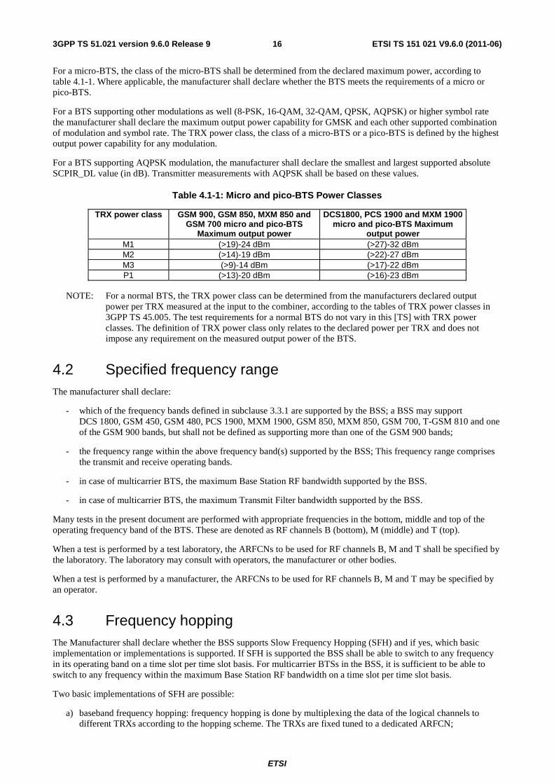
For a micro-BTS, the class of the micro-BTS shall be determined from the declared maximum power, according to table 4.1-1. Where applicable, the manufacturer shall declare whether the BTS meets the requirements of a micro or pico-BTS.
For a BTS supporting other modulations as well (8-PSK, 16-QAM, 32-QAM, QPSK, AQPSK) or higher symbol rate the manufacturer shall declare the maximum output power capability for GMSK and each other supported combination of modulation and symbol rate. The TRX power class, the class of a micro-BTS or a pico-BTS is defined by the highest output power capability for any modulation.
For a BTS supporting AQPSK modulation, the manufacturer shall declare the smallest and largest supported absolute SCPIR_DL value (in dB). Transmitter measurements with AQPSK shall be based on these values.
Table 4.1-1: Micro and pico-BTS Power Classes
TRX power class GSM 900, GSM 850, MXM 850 and GSM 700 micro and pico-BTS
Maximum output power
DCS1800, PCS 1900 and MXM 1900 micro and pico-BTS Maximum
output power M1 (>19)-24 dBm (>27)-32 dBm M2 (>14)-19 dBm (>22)-27 dBm M3 (>9)-14 dBm (>17)-22 dBm P1 (>13)-20 dBm (>16)-23 dBm
NOTE: For a normal BTS, the TRX power class can be determined from the manufacturers declared output
power per TRX measured at the input to the combiner, according to the tables of TRX power classes in 3GPP TS 45.005. The test requirements for a normal BTS do not vary in this [TS] with TRX power classes. The definition of TRX power class only relates to the declared power per TRX and does not impose any requirement on the measured output power of the BTS.
4.2 Specified frequency range The manufacturer shall declare:
- which of the frequency bands defined in subclause 3.3.1 are supported by the BSS; a BSS may support DCS 1800, GSM 450, GSM 480, PCS 1900, MXM 1900, GSM 850, MXM 850, GSM 700, T-GSM 810 and one of the GSM 900 bands, but shall not be defined as supporting more than one of the GSM 900 bands;
- the frequency range within the above frequency band(s) supported by the BSS; This frequency range comprises the transmit and receive operating bands.
- in case of multicarrier BTS, the maximum Base Station RF bandwidth supported by the BSS.
- in case of multicarrier BTS, the maximum Transmit Filter bandwidth supported by the BSS.
Many tests in the present document are performed with appropriate frequencies in the bottom, middle and top of the operating frequency band of the BTS. These are denoted as RF channels B (bottom), M (middle) and T (top).
When a test is performed by a test laboratory, the ARFCNs to be used for RF channels B, M and T shall be specified by the laboratory. The laboratory may consult with operators, the manufacturer or other bodies.
When a test is performed by a manufacturer, the ARFCNs to be used for RF channels B, M and T may be specified by an operator.
4.3 Frequency hopping The Manufacturer shall declare whether the BSS supports Slow Frequency Hopping (SFH) and if yes, which basic implementation or implementations is supported. If SFH is supported the BSS shall be able to switch to any frequency in its operating band on a time slot per time slot basis. For multicarrier BTSs in the BSS, it is sufficient to be able to switch to any frequency within the maximum Base Station RF bandwidth on a time slot per time slot basis.
Two basic implementations of SFH are possible:
a) baseband frequency hopping: frequency hopping is done by multiplexing the data of the logical channels to different TRXs according to the hopping scheme. The TRXs are fixed tuned to a dedicated ARFCN;

ETSI
ETSI TS 151 021 V9.6.0 (2011-06)173GPP TS 51.021 version 9.6.0 Release 9
b) synthesizer frequency hopping: frequency hopping is done by tuning the TRX on a timeslot per timeslot basis. The logical channels are dedicated to a hopping TRX.
The detailed description of the frequency hopping scheme is described in 3GPP TS 45.002.
4.4 RF power control RF power control functions ("dynamic power control") may optionally be implemented in GSM Base Station Systems according to 3GPP TS 45.008 as an operator choice. If implemented, the BSS shall be able to hop between any defined power level on a time slot per time slot basis. The manufacturer shall declare how many static power steps and how many dynamic steps are supported by the BSS. The number of static power steps and the total number of power control steps may be different for GMSK and other modulations (8-PSK, 16-QAM, 32-QAM, QPSK, AQPSK).
4.5 Downlink discontinuous transmission (DTX) Downlink discontinuous transmission (DTX), as defined in the GSM 06-series of specifications for full-rate speech channels and in 3GPP TS 24.022 [30] and 3GPP TS 48.020 [31] for non-transparent data, may optionally be implemented in the downlink BSS (transmitter) as an operator choice. All requirements in the present document, unless otherwise stated, apply whether downlink DTX is used or not.
4.6 Test environments For each test in the present document, the environmental conditions under which the BSS is to be tested are defined:
4.6.1 Normal test environment
When a normal test environment is specified for a test, the test should be performed under any combination of conditions between the minimum and maximum limits stated in table 4.6-1.
Table 4.6-1: Limits of conditions for Normal Test Environment
Condition Minimum Maximum Barometric pressure 86 kPa 106 kPa Temperature 15°C 30°C Relative Humidity 20 % 85 % Power supply Nominal, as declared by the manufacturer Vibration Negligible
The ranges of barometric pressure, temperature and humidity represent the maximum variation expected in the uncontrolled environment of a test laboratory. If it is not possible to maintain these parameters within the specified limits, the actual values shall be recorded in the test report.
NOTE: This may, for instance, be the case for measurements of radiated emissions performed on an open field test site.
4.6.2 Extreme test environment
The manufacturer shall declare one of the following:
a) the equipment class for the equipment under test, as defined in EN 300 019-1-3 , (Equipment Engineering (EE) [26]; Environmental conditions and environmental test for telecommunications equipment, Part 1-3: Classification of environmental conditions, Stationary use at weather protected locations);
b) the equipment class for the equipment under test, as defined in EN 300 019-1-4 , (Equipment Engineering (EE) [27]; Environmental conditions and environmental test for telecommunications equipment, Part 1-4: Classification of environmental conditions, Stationary use at non-weather protected locations);
ETSI
ETSI TS 151 021 V9.6.0 (2011-06)183GPP TS 51.021 version 9.6.0 Release 9
c) for equipment that does not comply to an EN 300 019-1 class [11], the relevant classes from IEC 60 721 [13] documentation for Temperature, Humidity and Vibration shall be declared, as defined in IEC 60 721-3-3 "Stationary use at weather protected locations" [28] or IEC 60 721-3-4 "Stationary use at non weather protected locations" [29] respectively.
NOTE: Reduced functionality for conditions that fall out side of the standard operational conditions are not tested in the present document. These may be stated and tested separately.
4.6.2.1 Extreme temperature
When an extreme temperature test environment is specified for a test, the test shall be performed at the standard minimum and maximum operating temperatures defined by the manufacturer's declaration for the equipment under test.
Minimum temperature:
- The test shall be performed with the environmental test equipment and methods of inducing the required environmental phenomena into the equipment, conforming to the test procedure of IEC 60068-2-1, Environmental Testing, Part 2: Tests - Tests A: Cold [12]. The equipment shall be maintained at the stabilized condition for the duration of the test sequence.
Maximum temperature:
- The test shall be performed with the environmental test equipment and methods of inducing the required environmental phenomena in to the equipment, conforming to the test procedure of IEC 60068-2-2 (Environmental Testing, Part 2: Tests - Tests Bd Dry heat) [12]. The equipment shall be maintained at the stabilized condition for the duration of the test sequence.
NOTE: It is recommended that the equipment is made fully operational prior to the equipment being taken to its lower operating temperature.
4.6.3 Vibration
When vibration conditions are specified for a test, the test shall be performed while the equipment is subjected to a vibration sequence as defined by the manufacturers declaration for the equipment under test. This shall use the environmental test equipment and methods of inducing the required environmental phenomena in to the equipment, conforming to the test procedure of IEC 60068-2-6, Environmental Testing, Part 2: Tests - Test Fc and guidance [12]: Vibration (Sinusoidal) or IEC 60068-2-64, Test Fh: Vibration broad-band random (digital control) and guidance. Other environmental conditions shall be within the ranges specified in subclause 4.6.1, Normal test environment.
NOTE: The higher levels of vibration may induce undue physical stress in to equipment after a prolonged series of tests. The testing body should only vibrate the equipment during the RF measurement process.
4.6.4 Power supply
When extreme power supply conditions are specified for a test, the test shall be performed at the standard upper and lower limits of operating voltage defined by the manufacturer's declaration for the equipment under test.
Upper voltage limit
The equipment shall be supplied with a voltage equal to the upper limit declared by the manufacturer (as measured at the input terminals to the equipment). The tests shall be carried out at the steady state minimum and maximum temperature limits declared by the manufacturer for the equipment, to the methods described in IEC 60 68-2-1 Test Ab/Ad: Cold and IEC 60068-2-2 Test Bb/Bd: Dry Heat [12].
Lower voltage limit
The equipment shall be supplied with a voltage equal to the lower limit declared by the manufacturer (as measured at the input terminals to the equipment). The tests shall be carried out at the steady state minimum and maximum temperature limits declared by the manufacturer for the equipment, to the methods described in IEC 60068-2-1 [12] Test Ab/Ad: Cold and IEC 60 068-2-2 Test Bb/Bd: Dry Heat [12].

ETSI
ETSI TS 151 021 V9.6.0 (2011-06)193GPP TS 51.021 version 9.6.0 Release 9
4.7 Acceptable uncertainty of measurement equipment The maximum acceptable uncertainty of measurement equipment is specified separately for each test, where appropriate. The measurement equipment shall enable the stimulus signals in the test case to be adjusted to within the specified tolerance, and the conformance requirement to be measured with an uncertainty not exceeding the specified values. All tolerances and uncertainties are absolute values, unless otherwise stated.
For the test methods, according to the present document, the measurement uncertainty figures shall be calculated in accordance with ETR 028 and shall correspond to an expansion factor (coverage factor) k = 1,96 or k = 2 (which provide confidence levels of respectively 95% and 95,45% in the case where the distributions characterising the actual measurement uncertainties are normal (Gaussian).
Subclause 4.6, Test environments:
Pressure ±5 kPa Temperature ±2 degrees Relative Humidity ±5 % DC Voltage ±1,0 % AC Voltage ±1,5 % Vibration 10 % Vibration frequency 0,1 Hz The above values shall apply unless the test environment is controlled and the specification for the control of the test environment specifies the uncertainty for the parameter.
Transmitter
Subclause 6.2, Modulation accuracy:
Conformance requirement:
Frequency, GMSK ±10 Hz ± 5 Hz for GSM 400
Phase 1,5 degree rms
5 degrees peak
EVM -(0,75 + 0,025RMS_EVM) – +(0,75 + 0,025RMV_EVM) % RMS
± 4 % for individual measurement samples
Origin Offset suppression ± 1,5 dB
Frequency , 8-PSK ± 16 Hz
16-QAM ± 6 Hz
32-QAM ± 6 Hz
QPSK ± 6 Hz
AQPSK ± [6] Hz
NOTE 1: The value of the RMS EVM specification is a function of the value of RMS_EVM being measured. The
asymmetric specification results from the RMS EVM minimisation method used for parameter estimation (see 3GPP TS 45.005, Annex G). This method of measurement for RMS EVM always produces a result that is lower than the actual value of RMS EVM.
NOTE 2: The value for individual EVM samples assumes a Rayleigh distribution of measurement errors. It represents the maximum 95th percentile value test equipment should return when measuring a signal without error.
Subclause 6.3, Mean transmitted RF carrier power:

ETSI
ETSI TS 151 021 V9.6.0 (2011-06)203GPP TS 51.021 version 9.6.0 Release 9
Conformance requirement:
RF power, for static power step 0 ±1,0 dB
Relative RF Power, for other power steps ±0,7 dB
Subclause 6.4, Transmitted RF carrier power versus time:
Conformance requirement
RF power (0 dB reference) ±1,0 dB
RF power relative to 0 dB reference ±10 dB
Subclause 6.5.1, Spectrum due to modulation and wideband noise:
Conformance requirement
RF power (absolute limit values) ±1,0 dB
NOTE 1: This may require calibration of the power levels corresponding to the limit values.
Relative RF power:
Offset from carrier, MHz Power difference, dB Uncertainty of relative power, dB δf ≤ 0.1 MHz All ±0,5 dB 0.1 MHz < δf ≤1.8 MHz < 50 dB ±0,7 dB 0.1 MHz < δf ≤1.8 MHz ≥ 50 dB ±1,5 dB > 1.8 MHz All ±2,0 dB
Subclause 6.5.2, Switching transients spectrum:
Conformance requirement:
RF power: ±1,5 dB
Relative RF power:
Power difference < 50 dB ±0,7 dB
Power difference ≥ 50 dB ±1,5 dB
Subclause 6.6.1, Conducted spurious emissions from the transmitter antenna connector, inside the BTS transmit band:
Conformance requirement:
RF power: ±1,5 dB
Subclause 6.6.2, Conducted spurious emissions from the transmitter antenna connector, outside the BTS transmit band:
Conformance requirement:
Conformance requirement i) (in the receive band of the BSS):
RF power ±3 dB
Conformance requirements ii), iii) and iv) (elsewhere):
RF power:
f ≤ 2 GHz ±1,5 dB
2 GHz < f ≤ 4 GHz ±2,0 dB
f > 4 GHz ±4,0 dB

ETSI
ETSI TS 151 021 V9.6.0 (2011-06)213GPP TS 51.021 version 9.6.0 Release 9
Subclause 6.7, Intermodulation attenuation and
Subclause 6.8, Intra base station system intermodulation attenuation:
Test case:
Relative RF power (of injected signal); ±1,5 dB
Conformance requirement (outside RX band):
RF power; absolute limit values ±1,5 dB
RF power, relative measurements ±2,0 dB
Conformance requirement (inside RX band):
RF power; absolute limit values +4 dB - 3 dB
NOTE 2: The positive limit for uncertainty is greater than the negative limit because the measurement result can be increased (but not decreased) due to intermodulation products within the measurement apparatus.
Receiver
Where a measurement uncertainty of +5 dB -0 dB is specified for an input signal, the measured value of the input signal should be increased by an amount equal to the uncertainty with which it can be measured. This will ensure that the true value of the input signal is not below the specified nominal.
Subclause 7.1, Static layer 1 receiver functions:
Test case
RF power, lower limit +5 - 0 dB
RF power, -40 dBm nominal ±2,5 dB
RF power, -23 and -15 dBm nominal ±1,5 dB
Subclause 7.2, Erroneous frame indication performance:
Test case:
RF Power +5 - 0 dB
Subclause 7.3, Static reference sensitivity level:
Test case:
RF power ±1,0 dB
Relative RF power ( adjacent timeslots) ±3,0 dB
Subclause 7.4, Multipath reference sensitivity level:
Test case:
RF power ±1,5 dB
Relative RF power ±3,0 dB
Subclause 7.5, Reference interference level:
Test case:
RF power +5 - 0 dB
Relative RF power ±1,0 dB

ETSI
ETSI TS 151 021 V9.6.0 (2011-06)223GPP TS 51.021 version 9.6.0 Release 9
NOTE 3: The measurement uncertainty for a faded (multipath) input signal may depend on the time taken to average the power of the b signal from the fader. It may be possible to reduce the measurement time by measuring the power with the fader set to the same class of fade profile, but with an increased fade rate.
Subclause 7.6, Blocking characteristics:
Test case:
RF power, wanted signal ±1,0 dB
RF power, interfering signal;
f ≤ 2 GHz ±0,7 dB
2 GHz < f ≤ 4 GHz ±1,5 dB
f > 4 GHz ±3,0 dB
Subclause 7.7, Intermodulation characteristics and subclause 7.8 AM suppression:
Test case:
RF power, wanted signal ±1,0 dB
RF power, interfering signals ±0,7 dB
Subclause 7.9, Spurious emissions from the receiver antenna connector:
Conformance requirement:
RF power;
f ≤ 2 GHz ±1,5 dB
2 GHz < f ≤ 4 GHz ±2,0 dB
f > 4 GHz ±4,0 dB
Clause 8, Radiated spurious emissions:
Conformance requirement:
RF power; ±6,0 dB
Clause 9, Radio link management:
Test case:
RF power ±1,0 dB
Relative RF power ±0,7 dB
Conformance requirement:
Timing difference single measurement ±1/4 bit
average of 100 measurements ±0,1 bit
4.8 Interpretation of measurement results The measurement value related to the corresponding limit shall be used to decide whether an equipment meets a requirement in the present document.
The measurement uncertainty for the measurement of each parameter shall be included in the test report.

ETSI
ETSI TS 151 021 V9.6.0 (2011-06)233GPP TS 51.021 version 9.6.0 Release 9
The recorded value for the measurement uncertainty shall be, for each measurement, equal to or lower than the appropriate figure in subclause 4.7 of the present document.
NOTE: This procedure is recommended in ETR 028.
If the measurement apparatus for a test is known to have a measurement uncertainty greater than that specified in subclause 4.7, it is still permitted to use this apparatus provided that an adjustment is made to the measured value as follows.
The adjustment is made by subtracting the modulus of the specified measurement uncertainty in subclause 4.7 from the measurement uncertainty of the apparatus. The measured value is then increased or decreased by the result of the subtraction, whichever is most unfavourable in relation to the limit.
4.9 Selection of configurations for testing Most tests in the present document are only performed for a subset of the possible combinations of test conditions. For instance:
- not all TRXs in the configuration may be specified to be tested;
- only one RF channel may be specified to be tested;
- only one timeslot may be specified to be tested.
When a test is performed by a test laboratory, the choice of which combinations are to be tested shall be specified by the laboratory. The laboratory may consult with operators, the manufacturer or other bodies.
When a test is performed by a manufacturer, the choice of which combinations are to be tested may be specified by an operator.
4.10 BTS Configurations The present document has been written to specify tests for the standard configurations of BTS which have been assumed in GSM requirements specifications, In particular GSM 05.01, 05.02 and 05.05. However, there are other configurations of BTS which comply with these specifications, but for which the application of these specifications is not fully defined. For some such configurations there may be alternate ways to apply the requirements of this specification to testing of the configuration, or some variation in the test method may be necessary. It may therefore be necessary for the parties to the testing to reach agreement over the method of testing in advance.
If the BSS is supplied in a number of different environmental enclosures or configurations, it may not be necessary to test RF parameters for each environmental configuration, provided that it can be demonstrated that the equipment has been tested at the worst internal environmental conditions
If a BTS is supplied with a number of different configurations of passive TX antenna combiners, there may be alternate ways to demonstrate the compliance rather than performing the measurements for each configuration. As an example, the worst case configuration of the antenna combiners for a given test shall as a minimum be used for this purpose.
Where alternative interpretations of this specification are possible for a BSS configuration under test, the interpretation which has been adopted in performing the test shall be recorded with the test results.
Where variation in the test method within the present document has been necessary to enable a BSS configuration to be tested, the variation in the test method which has been made in performing the test shall be recorded with the test results. Where possible, agreement should be reached in advance about the nature of such a variation with any party who will later receive the test results.
Possible interpretations of the present document for some common configurations are given in the following subclauses.
4.10.1 Receiver diversity
i) For the tests in clause 7 of the present document, the specified test signals may be applied to one receiver antenna connector, with the remaining receiver antenna connectors being terminated with 50 ohms.

ETSI
ETSI TS 151 021 V9.6.0 (2011-06)243GPP TS 51.021 version 9.6.0 Release 9
or
ii) For the tests in clause 7 of the present document, the specified test signals may be simultaneously applied to each of the receiver antenna connectors.
4.10.2 Duplexers
The requirements of the present document shall be met with a duplexer fitted, if a duplexer is supplied as part of the BSS. If the duplexer is supplied as an option by the manufacturer, sufficient tests should be repeated with and without the duplexer fitted to verify that the BSS meets the requirements of the present document in both cases.
The following tests should be performed with the duplexer fitted, and without it fitted if this is an option.
1) Subclause 6.3, Mean transmitted RF power, for the highest static power step only, if this is measured at the antenna connector.
2) Subclause 6.6.2, Conducted spurious emissions from the transmitter antenna connector; outside the BTS transmit band.
3) Subclause 6.8, Intra base station system intermodulation attenuation.
4) Subclause 7.4, Multipath reference sensitivity; for the testing of essential conformance, the ARFCNs should be selected to minimize intermodulation products from the transmitters falling in receive channels.
The remaining tests may be performed with or without the duplexer fitted.
NOTE 1: When performing receiver tests with a duplexer fitted, it is important to ensure that the output from the transmitters does not affect the test apparatus. This can be achieved using a combination of attenuators, isolators and filters.
NOTE 2: When duplexers are used, intermodulation products will be generated, not only in the duplexer but also in the antenna system. The intermodulation products generated in the antenna system are not controlled by ETSI specifications, and may degrade during operation (e.g. due to moisture ingress). Therefore, to ensure continued satisfactory operation of a BSS, an operator will normally select ARFCNs to minimize intermodulation products falling on receive channels. For testing of complete conformance, an operator may specify the ARFCNs to be used.
4.10.3 Power supply options
If the BSS is supplied with a number of different power supply configurations, it may not be necessary to test RF parameters for each of the power supply options, provided that it can be demonstrated that the range of conditions over which the equipment is tested is at least as great as the range of conditions due to any of the power supply configurations.
This applies particularly if a BSS contains a DC rail which can be supplied either externally or from an internal mains power supply. In this case, the conditions of extreme power supply for the mains power supply options can be tested by testing only the external DC supply option. The range of DC input voltages for the test should be sufficient to verify the performance with any of the power supplies, over its range of operating conditions within the BTS, including variation of mains input voltage, temperature and output current.
4.10.4 Ancillary RF amplifiers
Ancillary RF amplifier: a piece of equipment, which when connected by RF coaxial cables to the BTS, has the primary function to provide amplification between the transmit and/or receive antenna connector of a BTS and an antenna without requiring any control signal to fulfil its amplifying function.
The requirements of the present document shall be met with the ancillary RF amplifier fitted. At tests according to clauses 6 and 7 for TX and RX respectively, the ancillary amplifier is connected to the BTS by a connecting network (including any cable(s), attenuator(s), etc.) with applicable loss to make sure the appropriate operating conditions of the ancillary amplifier and the BTS. The applicable connecting network loss range is declared by the manufacturer. Other characteristics and the temperature dependence of the attenuation of the connecting network are neglected. The actual attenuation value of the connecting network is chosen for each test as one of the applicable extreme values. The lowest value is used unless otherwise stated.

ETSI
ETSI TS 151 021 V9.6.0 (2011-06)253GPP TS 51.021 version 9.6.0 Release 9
Sufficient tests should be repeated with the ancillary amplifier fitted and, if it is optional, without the ancillary RF amplifier to verify that the BSS meets the requirements of the present document in both cases.
When testing for essential conformance, the following tests should be repeated with the optional ancillary amplifier fitted according to the table below, where x denotes that the test is applicable:
Subclause TX amplifier only RX amplifier only TX/RX amplifiers combined (Note)
Receiver 7.3 x x tests 7.6 x x
7.7 x x 7.9 x 6.3 x x
Transmitter 6.5 (6.5.1 only) x x tests 6.6 x x
6.7 x x 6.8 x x
NOTE: Combining can be by duplex filters or any other network. The amplifiers can either be in RX or TX
branch or in both. Either one of these amplifiers could be a passive network.
For receiver tests only testing on TCH/FS is required
In test according to subclause 7.3 and 6.3 highest applicable attenuation value is applied.
4.10.5 BSS using antenna arrays
A BSS may be configured with a multiple antenna port connection for some or all of its TRXs or with an antenna array related to one cell (not one array per TRX). This section applies to a BSS which meets at least one of the following conditions:
- the transmitter output signals from one or more TRX appear at more than one antenna port; or
- there is more than one receiver antenna port for a TRX or per cell and an input signal is required at more than one port for the correct operation of the receiver (NOTE: diversity reception does not meet this requirement) thus the outputs from the transmitters as well as the inputs to the receivers are directly connected to several antennas (known as „air combining"); or
- transmitters and receivers are connected via duplexers to more than one antenna.
If a BSS is used, in normal operation, in conjunction with an antenna system which contains filters or active elements which are necessary to meet the GSM requirements, the tests of essential conformance may be performed on a system comprising the BSS together with these elements, supplied separately for the purposes of testing. In this case, it must be demonstrated that the performance of the configuration under test is representative of the system in normal operation, and the conformance assessment is only applicable when the BSS is used with the antenna system.
For testing of essential conformance of such a BSS, the following procedure may be used.
Receiver tests
For each test, the test signals applied to the receiver antenna connectors shall be such that the sum of the powers of the signals applied equals the power of the test signal(s) specified in the test.
An example of a suitable test configuration is shown in figure 4.10-1.
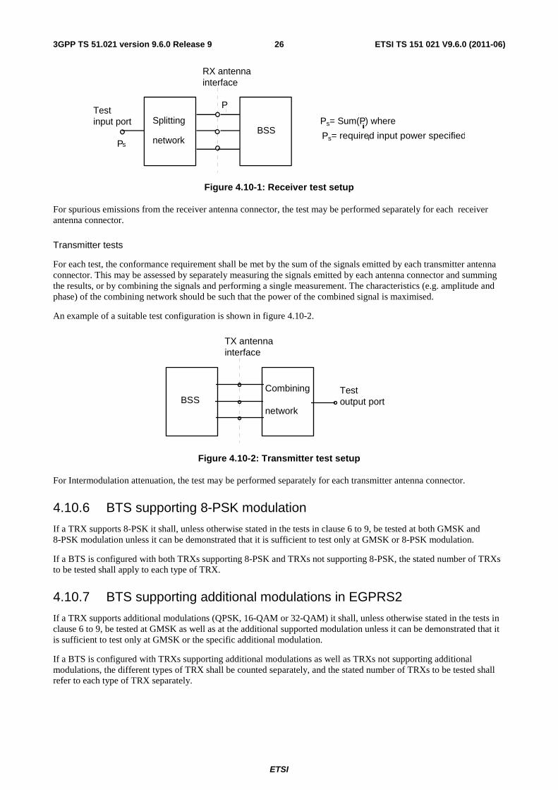
ETSI
ETSI TS 151 021 V9.6.0 (2011-06)263GPP TS 51.021 version 9.6.0 Release 9
RX antennainterface
Splitting
network
Testinput port
BSS
Pi
Ps= Sum(Pi) where
PsPs= required input power specifiedi
Figure 4.10-1: Receiver test setup
For spurious emissions from the receiver antenna connector, the test may be performed separately for each receiver antenna connector.
Transmitter tests
For each test, the conformance requirement shall be met by the sum of the signals emitted by each transmitter antenna connector. This may be assessed by separately measuring the signals emitted by each antenna connector and summing the results, or by combining the signals and performing a single measurement. The characteristics (e.g. amplitude and phase) of the combining network should be such that the power of the combined signal is maximised.
An example of a suitable test configuration is shown in figure 4.10-2.
TX antennainterface
Combining
network
Testoutput portBSS
Figure 4.10-2: Transmitter test setup
For Intermodulation attenuation, the test may be performed separately for each transmitter antenna connector.
4.10.6 BTS supporting 8-PSK modulation
If a TRX supports 8-PSK it shall, unless otherwise stated in the tests in clause 6 to 9, be tested at both GMSK and 8-PSK modulation unless it can be demonstrated that it is sufficient to test only at GMSK or 8-PSK modulation.
If a BTS is configured with both TRXs supporting 8-PSK and TRXs not supporting 8-PSK, the stated number of TRXs to be tested shall apply to each type of TRX.
4.10.7 BTS supporting additional modulations in EGPRS2
If a TRX supports additional modulations (QPSK, 16-QAM or 32-QAM) it shall, unless otherwise stated in the tests in clause 6 to 9, be tested at GMSK as well as at the additional supported modulation unless it can be demonstrated that it is sufficient to test only at GMSK or the specific additional modulation.
If a BTS is configured with TRXs supporting additional modulations as well as TRXs not supporting additional modulations, the different types of TRX shall be counted separately, and the stated number of TRXs to be tested shall refer to each type of TRX separately.

ETSI
ETSI TS 151 021 V9.6.0 (2011-06)273GPP TS 51.021 version 9.6.0 Release 9
4.10.8 Supported Symbol Rate
The tests in this specification are applicable to both normal symbol rate and higher symbol rate configurations, unless otherwise stated.
4.10.9 Support of RTTI and/or FANR
All tests are performed for BTTI configuration and without PAN, unless otherwise stated. Additional tests marked as specifically RTTI requirements without and with PAN, as well as BTTI with PAN shall be performed if BTS is declared to support these features.
4.10.10 Multicarrier BTS
If the BTS belongs to the multicarrier BTS class the configuration and number of TRXs to be used in the test corresponds to the configuration and number of active carriers at each transmitting antenna connector (i.e. at each transmitter output of a multicarrier transmitter or transceiver). The tests shall be repeated for each transmitting antenna connector, if connected to a multicarrier transmitter. If the maximum Base Station RF bandwidth is less than the relevant transmit band, and the transmitter is capable of operating on all parts of the relevant transmit band or a declared part of it (operating TX band according to subclause 4.2) by tuning, the transmitter tests are repeated until the whole relevant transmit band or the declared operating band is tested.
For multicarrier BTS testing, when the definition minimum frequency spacing is used, the carrier spacing of 600 kHz shall apply for that test case.
The tests in this specification are based on the testing of multicarrier configurations for the supported numbers of carriers, operating at declared maximum power for each number of carriers equally distributed among the carriers. All supported numbers of carriers shall be included in the tests unless otherwise stated in the test case. Equipment that passes all the tests in this specification shall also comply in other configurations, with unequal distribution of power among the carriers, as long as these configurations are defined within the limits of total power, power control margin and maximum number of carriers in the multicarrier transmitter. To verify this compliance a test case with unequal power distribution shall be tested when stated in the subclause:
• If support of four or more active carriers is declared: two carriers are configured to 2 dB higher power and two to 4 dB lower power than the declared maximum power at equal distribution. Any additional carrier shall be configured to the declared maximum power at equal distribution. If one carrier needs to be defined as BCCH carrier according to test case, the carrier with highest power shall be used for BCCH.
• If support of less than four active carriers is declared: One carrier is configured to 2 dB higher power and one to 4 dB lower power than the declared maximum power at equal distribution. Any additional carrier shall be configured to the declared maximum power at equal distribution. If one carrier needs to be defined as BCCH carrier according to test case, the carriers with highest power shall be used for BCCH.
If the BTS belongs to the multicarrier BTS class the manufacturer shall declare the supported combinations of number of carriers, output powers and the maximum Base Station RF bandwidth.
The manufacturer shall also declare if the multicarrier BTS is equipped with multicarrier receiver and any equivalent receiver paths. The tests shall be repeated for each antenna connector, if connected to a multicarrier receiver. It is sufficient to test one of the equivalent receiver paths. If the maximum Base Station RF bandwidth is less than the relevant receive band, and the receiver is capable of operating on all parts of the relevant receive band or a declared part of it (operating RX band according to subclause 4.2) by tuning, the receiver tests are repeated until the whole relevant receive band or the declared operating band is tested.
For any test that applies to a multicarrier BTS with multicarrier receiver, the required receiver resources for the maximum supported number of wanted signals shall be allocated and activated simultaneously at frequencies as evenly distributed as possible over the declared maximum Base Station RF bandwidth including the band edges of the Base Station RF bandwidth during the complete test, unless otherwise stated. The actual number and allocation of the applied input signals shall be as defined in each respective test. In case the supported maximum number of signals is higher than the number of applied wanted signals the remaining resources are allocated and activated for frequencies, not under test.
The declared configuration and stated performance shall be tested and fulfilled for any channel using the resource allocation and input signal configuration stated above.

ETSI
ETSI TS 151 021 V9.6.0 (2011-06)283GPP TS 51.021 version 9.6.0 Release 9
For any test that applies to a multicarrier configuration in case of a multicarrier BTS all carriers shall apply the GMSK modulation, unless otherwise stated.
In test cases regarding unwanted emissions inband, i.e. including spectrum due to modulation and wideband noise, spurious emissions and Intermodulation attenuation, detector mode AVG or RMS can be used for conformance testing. If the requirements are fulfilled in either detector mode, the tests are sufficient for compliance. The detector mode used, shall be stated in the conformance test report.
The vendor shall declare if the multicarrier BTS supports non-contiguous frequency allocation, defined as an allocation where two groups of frequencies are separated with at least 5.4 MHz.
5 Format and interpretation of tests Each test in the following clauses has a standard format:
X Title
All tests are applicable to all equipment within the scope of this specification, unless the title of the test is Applicability (Phase 2) or Applicability (Phase 2+), and the applicability is defined below.
X.1 Test purpose
This subclause defines the purpose of the test.
X.2 Test case
This subclause describes the steps necessary to perform the test. The general test conditions described in clause 4 also apply.
X.3 Essential conformance
The essential conformance describes the conformance requirements necessary to ensure compatibility and to verify the important aspects of the transmission quality of the system. This subclause is divided into two parts:
Test environment
This subclause describes the test environment or environments under which the test shall be performed. Where more than one test environment is specified, the extent of testing is specified for each environment.
Conformance requirement
This subclause describes the requirement which shall be met for the specified tests.
The test case describes the testing for full conformance; for most tests a subset of these tests is specified for essential conformance. Therefore, any definition of testing in the essential conformance shall take precedence over the test case.
X.4 Complete conformance
The complete conformance describes the complete set of tests which may be performed to fully characterize all aspects of one performance parameter of the BSS.
Test environment
This subclause describes the test environment or environments under which the test shall be performed. Where more than one test environment is specified, the extent of testing is specified for each environment.
Conformance requirement
This subclause describes the requirement which shall be met for the specified tests.
X.5 Requirement reference
This subclause gives the reference to the subclauses in the GSM specifications from which the test requirements have been derived. Where the Requirement reference subclause references the ETSs corresponding to both the Phase 2 and Phase 2+ versions of the same GSM specification, the Phase 2 and Phase 2+ requirements which are referenced are

ETSI
ETSI TS 151 021 V9.6.0 (2011-06)293GPP TS 51.021 version 9.6.0 Release 9
consistent. If the test case and/or requirements are different for Phase 2 (ETS) and the various releases of Phase 2+ (3GPP TS), this is stated in the applicability part of the subclause. When no applicability is stated the requirements are consistent and the referenced requirements apply to all referenced specifications (ETS or TS).
6 Transmitter All tests in this Clause shall be conducted on Base Station Systems fitted with a full complement of Transceivers for the configuration unless otherwise stated. Measurements shall be made at the BTS Tx antenna connector, unless otherwise stated.
Power levels are expressed in dBm.
For measurements in VAMOS mode, VAMOS sub-channel 1 shall use TSC-5 from TSC Set 1 and VAMOS sub-channel 2 shall use TSC-5 from TSC Set 2. Independent pseudo random bit streams shall be assumed for the encrypted bits of VAMOS sub-channel 1 and VAMOS sub-channel 2. Measurements shall be performed for the smallest and largest supported absolute SCPIR_DL value (in dB) unless otherwise stated.
6.1 Static Layer 1 functions
6.1.1 Test purpose
To verify the following static Layer 1 transmitter functions:
1) the RF equipment;
2) the multiplexing and multiple access functions;
3) the interleaving and the channel encoding on the transmit side.
6.1.2 Test case
The BSS shall be configured with the maximum number of TRXs, with ARFCNs which shall be distributed over the entire declared bandwidth of operation for the BSS under test. One TRX shall be configured to support the BCCH. If the manufacturer declares that slow frequency hopping is supported, this shall be enabled.
Each TRX shall transmit a normal GSM modulated signal and the BSSTE shall be connected to the transmitter antenna connector. A known bit sequence exceeding a length of a superframe (1326 TDMA-frames) shall be input before channel encoding in the BSS and a bit sequence shall be output after channel decoding in the BSSTE.
All logical channel types supported by the BSS shall be tested. The test shall be repeated for each TRX in the BSS configuration, for each logical channel supported by it.
NOTE: Some logical channels are only supported by the TRX configured to support the BCCH.
For measurements in VAMOS mode the test shall be performed on both VAMOS sub-channels for the smallest supported absolute SCPIR_DL value (in dB).
6.1.3 Essential conformance
This test need not be performed.
6.1.4 Complete conformance
Test Environment
Normal.
Conformance requirement

ETSI
ETSI TS 151 021 V9.6.0 (2011-06)303GPP TS 51.021 version 9.6.0 Release 9
The output bit sequence shall be bit exact for all logical channel types.
6.1.5 Requirement reference
3GPP TS 45.001, 3GPP TS 45.002, 3GPP TS 45.003 and 3GPP TS 45.005.
6.2 Modulation accuracy
6.2.1 Test purpose
1) To verify the correct implementation of the pulse shaping filtering.
2) To verify that at GMSK modulation the phase error during the active part of the time slot does not exceed the specified limits under normal and extreme test conditions and when subjected to vibration.
3) To verify that the frequency error during the active part of the time slot does not exceed the specified limits under normal and extreme test conditions and when subjected to vibration.
4) To verify that at supported modulations 8-PSK, QPSK, AQPSK, 16-QAM and 32-QAM the Error Vector Magnitude (EVM) and the origin offset during the active part of the time slot do not exceed the specified limits under normal and extreme test conditions and when subjected to vibration.
6.2.2 Test case
All TRXs in the configuration shall be switched on transmitting full power in all time slots for at least 1 hour before starting the test.
In case of a multicarrier BTS, the tests shall be performed with one carrier active and with the declared maximum number of carriers active at declared maximum output power equally distributed.
If the Manufacturer declares that Synthesizer Slow Frequency Hopping is supported by the BSS, the BSS shall be configured with the maximum number of TRXs with ARFCNs which shall be distributed over the entire declared bandwidth of operation for the BSS under test, and including B, M and T, and three tests shall be performed. These tests may either use a test apparatus which employs the same hopping sequence as the BSS, or a fixed frequency apparatus on the radio frequency channels B, M and T. If only Baseband SFH is supported or SFH is not supported, one test shall be performed for each of the radio frequency channels B, M and T, using different TRXs to the extent possible for the configuration. As a minimum, one time slot shall be tested on each TRX specified to be tested.
GMSK modulation
The transmitted GMSK modulated signal from the TRX under test shall be extracted in the BSSTE for a pseudo-random known bit stream of encrypted bits into the TRX modulator (the BSSTE is defined in annex B.1). The pseudo-random bit stream shall be any 148 bit sub-sequence of the 511 bit pseudo-random bit stream defined in recommendation CCITT Q.153 fascicle IV.4. This pseudo-random bit stream may be generated by another pseudo-random bit stream inserted before channel encoding in the TRX and shall generate at least 200 different bursts. The phase trajectory (phase versus time) for the useful part of the time slots (147 bits in the centre of the burst - see 3GPP TS 45.004 and 3GPP TS 45.010 for further information) shall be extracted with a resolution of at least 2 samples per modulating bit. The RF receiver parts of the BSSTE shall not limit the measurement.
The theoretical phase trajectory from the known pseudo-random bit stream shall be calculated in the BSSTE.
The phase difference trajectory shall be calculated as the difference between the measured and the theoretical phase trajectory. The mean frequency error across the burst shall then be calculated as the derivative of the regression line of the phase difference trajectory. The regression line shall be calculated using the Mean Square Error (MSE) method.
The phase error is then finally the difference between the phase difference trajectory and its linear regression line.
ETSI
ETSI TS 151 021 V9.6.0 (2011-06)313GPP TS 51.021 version 9.6.0 Release 9
8-PSK, QPSK, AQPSK, 16-QAM and 32-QAM modulation
The transmitted 8-PSK, QPSK, AQPSK, 16-QAM or 32-QAM modulated signal from the TRX under test shall be extracted in the BSSTE for a pseudo-random known bit stream of encrypted bits into the TRX modulator (the BSSTE is defined in annex B.1). The pseudo-random bit stream shall be any bit sub-sequence of the 32767-bit pseudo-random bit stream defined in recommendation CCITT O.151 10/1997.
The error vector between the vector representing the transmitted signal and the vector representing the error-free modulated signal defines modulation accuracy. The magnitude of the error vector is called Error Vector Magnitude (EVM). Origin suppression is defined to be the ratio of the carrier leakage to the modulated signal. For definition and calculation of EVM, see 3GPP TS 45.005 Annex G.
The following steps 1) to 5) shall be performed according to 3GPP TS 45.005 subclause 4.6.2 and annex G.
1) The RMS EVM shall be measured and calculated over the useful part of the burst (excluding tail bits) for at least 200 bursts.
2) The origin offset suppression shall be measured and calculated.
3) The frequency offset shall be measured and calculated.
4) The peak EVM shall be measured and calculated. The peak EVM is the peak error deviation within a burst, measured at each symbol interval, averaged over at least 200 bursts. The bursts shall have a minimum distance in time of 7 idle timeslots between them. The peak EVM values are acquired during the useful part of the burst, excluding tail bits.
5) The 95:th percentile EVM shall be measured and calculated. The 95:th percentile EVM is the point where 95% of the individual EVM, measured at each symbol interval, is below that point. That is, only 5% of the symbols are allowed to have an EVM exceeding the 95:th-percentile point. The EVM values are acquired during the useful part of the burst, excluding tail bits, over 200 bursts.
6.2.3 Essential conformance
Test Environment
Normal: One test shall be performed on each of B, M and T.
Extreme Power supply: One test shall be performed on each of B, M and T.
NOTE: tests under extreme power supply are carried out at extreme temperature limits.
In case of multicarrier BTS the tests shall be performed for single carrier operation at B, M and T of the operating transmit band, and with declared maximum number of carriers distributed according to test case b) in subclause 6.12.2 throughout the maximum Base Station RF bandwidth. For the test with maximum number of carriers, all carriers shall apply the same modulation type and operate at equal, maximum declared carrier power for this modulation type. The test shall be repeated for each modulation type supported by the multicarrier BTS.
Conformance requirement
GMSK modulation
The phase error shall not exceed:
5 degrees rms
20 degrees peak
For normal and micro BTSs the mean frequency error across the burst shall not exceed:
0,05 ppm
For pico BTSs the mean frequency error across the burst shall not exceed:
0,1 ppm
Higher order modulation

ETSI
ETSI TS 151 021 V9.6.0 (2011-06)323GPP TS 51.021 version 9.6.0 Release 9
The RMS EVM values, measured after any active element and excluding the effect of passive combining equipment, shall not exceed:
Normal symbol rate Higher symbol rate
AQPSK 8-PSK 16-QAM
32-QAM
QPSK 16-QAM
32-QAM
under normal conditions
[tbd] 7,0 % 5,0 % 5,0 % 7,0 % 4,0 % 4,0 %
under extreme conditions
[tbd] 8,0 % 6,0 % 6,0 % 8,0 % 5,0 % 5,0 %
The RMS EVM values, measured after any active element and including the effect of passive combining equipment, shall not exceed:
Normal symbol rate Higher symbol rate
AQPSK 8-PSK 16-QAM
32-QAM
QPSK 16-QAM
32-QAM
under normal conditions
[tbd] 8,0 % 6,0 % 6,0 % 8,0 % 5,5 % 5,5 %
under extreme conditions
[tbd] 9,0 % 7,0 % 7,0 % 9,0 % 6,5 % 6,5 %
The origin offset suppression shall exceed:
35 dB
For normal and micro BTSs the frequency offset shall not exceed:
0,05 ppm
For pico BTSs the frequency offset shall not exceed:
0,1 ppm
The peak EVM values, excluding the effect of passive combining equipment, shall not exceed:
22 %
The 95:th percentile EVM value, excluding the effect of passive combining equipment, shall not exceed:
11 %
6.2.4 Complete conformance
Test Environment
Normal: The test shall be repeated until 3 TRXs or all TRXs (whichever is the less) have each been tested on B, M and T.
Extreme Power supply: One test shall be performed on each of B, M and T.
NOTE: tests under extreme power supply are carried out at extreme temperature limits.
Vibration : One test shall be performed on each of B, M and T.

ETSI
ETSI TS 151 021 V9.6.0 (2011-06)333GPP TS 51.021 version 9.6.0 Release 9
In case of multicarrier BTS the test shall be performed for single carrier operation at B, M and T of the operating transmit band, and with declared maximum number of carriers distributed according to test case b) in subclause 6.12.2 throughout the maximum Base Station RF bandwidth, except in vibration conditions as stated in subclause 4.6.3 where only single active carrier operation need to be tested.
Conformance requirement
The requirement of essential conformance shall apply.
6.2.5 Requirement reference
3GPP TS 45.004, clause 2; 3GPP TS 45.005, subclause 4.6; 3GPP TS 45.010, subclause 5.1.
6.3 Mean transmitted RF carrier power
6.3.1 Test purpose
To verify the accuracy of the mean transmitted RF carrier power across the frequency range and at each power step.
This test is also used to determine the parameter "power level", used in subclause 6.5.1.2.
6.3.2 Test case
For a normal BTS, this measurement the power shall be measured at the input of the TX combiner or at the BSS antenna connector. For a micro-BTS, the power shall be measured at the BSS antenna connector. For a multicarrier BTS the power shall be measured at each transmitting BSS antenna connector. The Manufacturer shall declare the maximum output power of the BSS for each supported modulation at the same reference point as the measurement is made. The TX combiner shall have the maximum number of TRXs connected to it so that the measurement can be used as a reference for the measurement of transmitted carrier power versus time in subclause 6.4.
NOTE: The value of the output power measured at the antenna connector is generally more useful for cell planning, and may be required for regulatory purposes
All TRXs in the configuration shall be switched on transmitting full power in all time slots for at least 1 hour before starting the test.
The Manufacturer shall declare how many TRXs the BSS supports:
1 TRX: The TRX shall be tested at B, M and T;
2 TRX: The TRXs shall each be tested at B, M and T;
3 TRX or more: Three TRXs shall each be tested at B, M and T.
In case of multicarrier BTS the tests shall be performed for the declared number(s) of carriers, operating at maximum and equally distributed power at minimum frequency spacing and grouped at B, M and T, for each antenna connector.
In addition the test case with unequal power distribution according to subclause 4.10.10 shall be performed for the declared maximum number of carriers.
If the Manufacturer declares that Synthesizer Slow Frequency Hopping is supported by the BSS, the BSS shall be configured with the number of TRXs and frequency allocation defined above and SFH enabled.
The BSS under test shall be set to transmit at least 3 adjacent time slots in a TDMA-frame at the same power level. The RMS power level shall be measured on a time slot basis over the useful part of one of the active time slots and then the average of the logarithmic value taken over at least 200 time slots. Only active bursts shall be included in the averaging process. Whether SFH is supported or not, the measurement shall be carried out on all of the 3 frequencies in turn. The measurement bandwidth shall be at least 300 kHz.
For the definition of the useful part of the time slot see figure 6.4-1, and for further details 3GPP TS 45.004 and 3GPP TS 45.010. For timing on a per time slot basis , in case of normal symbol rate, each time slot may contain 156.25 modulating symbols, or 2 time slots may contain 157 and 6 time slots 156 modulating symbols according to 3GPP

ETSI
ETSI TS 151 021 V9.6.0 (2011-06)343GPP TS 51.021 version 9.6.0 Release 9
TS 45.010. In case of higher symbol rate each time slot may contain 187,5 symbols or 188,4 symbols on timeslot 0 and 4 and 187,2 symbols on the remaining timeslots in a TDMA-frame according to 3GPP TS 45.010.
The power shall be measured at each nominal power level as specified. As a minimum, one time slot shall be tested on each TRX. Any TRX which is a dedicated BCCH shall only be tested at highest static power step.
6.3.3 Essential conformance
Test Environment
Normal: Each TRX specified in the test case shall be tested.
Extreme power supply: One TRX shall be tested, on one ARFCN, for highest static power step only.
NOTE: tests under extreme power supply are carried out at extreme temperature limits.
Conformance requirement
The BSS shall support Nmax steps of Static Power Control for each supported modulation with respect to the declared output power as declared by the manufacturer. For the modulation with the highest output power, Nmax shall be at least 6.
The static power step N has the range from the highest static power level to Nmax inclusive, where
- The Highest Static Power Level corresponds to the maximum single carrier output power declared by the manufacturer. For multicarrier BTS, the Highest Static Power Level corresponds to maximum output power per carrier for each supported number of carriers declared by the manufacturer.
- The Lowest Static Power Level is defined as the Highest Static Power Level reduced by Nmax power steps, where the number of power steps can be different for each supported modulation.
The power measured when the TRX is set to Highest Static Power Control Level shall have a tolerance of ±2 dB under normal conditions and ±2,5 dB under extreme conditions, relative to the maximum power declared by the manufacturer for the modulation under test. In this test, this measured power is termed the maximum BTS output power. Static power control shall allow the RF output power to be reduced from the maximum BTS output power for the modulation with the highest output power capability in at least 6 steps of nominally 2 dB with a tolerance of ±1 dB for each modulation referenced to the previous level of the same modulation. In addition, the actual absolute output power for each supported modulation at each static RF power step (N) , with the exception below for the highest RF power level for 8-PSK, QPSK, AQPSK, 16-QAM and 32-QAM, shall be 2*N dB below the maximum BTS output power for the modulation with the highest output power capability with a tolerance of ±3 dB under normal conditions and ±4 dB under extreme conditions.
In addition to the Static Power Control levels the BSS may utilize up to M steps of dynamic Downlink Power Control. M can have an upper limit of 0 to 15.
Dynamic Downlink power control shall allow the RF output power to be reduced in M steps with a step size of 2 dB with a tolerance of ±1,5 dB referenced to the previous level.
Each dynamic Downlink Power Control level shall have a tolerance of ±3 dB under normal conditions and ±4 dB under extreme conditions relative to 2*Y dB below the maximum BTS output power for the modulation with the highest output power capability, where Y is the sum of the number of static and dynamic steps below Highest Static Power Control Level for the modulation with the highest output power capability.
For BTS supporting 8-PSK, QPSK, AQPSK, 16-QAM and/or 32-QAM the output power for GMSK, 8-PSK, QPSK, AQPSK, 16-QAM and 32-QAM shall be nominally the same for any supported static and dynamic power control level. An exception is allowed for the maximum output power of the respective modulation QPSK, AQPSK, 8-PSK, 16-QAM and 32-QAM, which may be lower than the GMSK output power for the same static or dynamic power control level. The nominal size of the first step down from the respective maximum power level of QPSK, 8-PSK, AQPSK, 16-QAM and 32-QAM may be in the range 0 to 2 dB. The output power of QPSK, 8-PSK, AQPSK, 16-QAM and 32-QAM for the respective second highest static or dynamic power control level shall be the same as the GMSK power for the corresponding static or dynamic power control level within a tolerance of ±1 dB The number of static RF power steps and the total number of power control steps may be different for GMSK and other supported modulations (8-PSK, QPSK, AQPSK, 16-QAM and 32-QAM).

ETSI
ETSI TS 151 021 V9.6.0 (2011-06)353GPP TS 51.021 version 9.6.0 Release 9
6.3.4 Complete conformance
The requirement of essential conformance shall apply.
6.3.5 Requirement reference
3GPP TS 45.005 subclause 4.1.2.
6.4 Transmitted RF carrier power versus time
6.4.1 Test purpose
To verify:
1) the time during which the transmitted power envelope should be stable (the useful part of the time slot);
2) the stability limits;
3) the maximum output power when nominally off between time slots.
It is not the purpose of this test to measure the detail of the power ramps; this is measured as adjacent channel power in subclause 6.5.
6.4.2 Test case
The Manufacturer shall declare how many TRXs the BSS supports, and declare any TRXs which are a dedicated BCCH carrier:
1 TRX: The BSS shall not be tested.
2 TRX: One TRX shall be configured to support the BCCH and the other shall be tested. Tests shall be performed on B, M and T, and both TRXs shall be tested on at least one frequency.
3 TRX: One TRX shall be configured to support the BCCH and the other two shall be tested at B, T and B, M. Tests shall be performed on B, M and T and both TRXs shall be tested on at least one frequency.
4 TRX or more: One TRX shall be configured to support the BCCH and three TRXs tested, one on B, one on M and one on T.
If the Manufacturer declares that Synthesizer Slow Frequency Hopping is supported by the BSS, the BSS shall be configured with the number of TRXs activated and frequency allocation defined above and SFH enabled. The TRX configured to support the BCCH shall not be tested.
If the TRX under test supports 8-PSK and/or other modulation(s), the test shall be performed at GMSK, 8-PSK and all other supported modulations.
A single time slot in a TDMA-frame shall be activated in all TRXs to be tested, all other time slots in the TDMA-frame shall be at Pidle.
Power measurements are made with a detector bandwidth of at least 300 kHz at the BTS antenna connector, at each frequency tested. Timing is related to T0 which, for the normal symbol rate case, is the transition time from symbol 13 to symbol 14 of the midamble training sequence for each time slot. For higher symbol rate T0 is defined as center of the 16th symbol. For timing on a per time slot basis each time slot, for the normal symbol rate case, may contain 156.25 modulating symbols, or 2 time slots may contain 157 and 6 time slots 156 modulating symbols according to 3GPP TS 45.010. In case of higher symbol rate each time slot may contain 187,5 symbols or 188,4 symbols on timeslot 0 and 4 and 187,2 symbols on the remaining timeslots in a TDMA-frame. Measurements shall be made at Pmax and Pmin. The time slots measured shall be displayed or stored for at least 100 complete cycles of the time slot power sequence for each measurement.
Pmax = Power measured in subclause 6.3 (Highest Static Power Control Level).

ETSI
ETSI TS 151 021 V9.6.0 (2011-06)363GPP TS 51.021 version 9.6.0 Release 9
Pmin = the Lowest Static Power Level measured in subclause 6.3.
Pidle Pmax -30 dB, or Pmin - 30 dB.
As a minimum, one time slot shall be tested on each TRX under test which is not a dedicated BCCH.
6.4.3 Essential conformance
Test Environment
Normal
Conformance requirement
The output power of each time slot tested relative to time shall conform with that illustrated in figure 6.4-1 and, if other modulations are supported, 6.4-2, 6.4-3, 6.4-4, 6.4-5 and 6.4-6. The residual output power, if a time slot is not activated, shall be maintained at, or below, the level of -30 dBc (300 kHz measurement bandwidth).
6.4.4 Complete conformance
The requirement of essential conformance shall apply.
power (dB)
-30 (Pidle)
-6
+4
useful part
147 bits
0
time (us)
147 bits = 542.8 us = 7056/13 us
1 timeslot = 576.9 us = 156.25 bits
T0
+1.0
-1.0
810 10 10 1087056/13 (542.8)
Power/time mask for GSM 400, GSM 900, DCS 1800, GSM 700, GSM 850 and MXM 850

ETSI
ETSI TS 151 021 V9.6.0 (2011-06)373GPP TS 51.021 version 9.6.0 Release 9
dB
t
- 30
+ 4
8µs 10µs 10µs 8µs7056/13 (542.8) µs 10µs
(*)10µs
- 1
+ 1
(147 bits)
0
Dashed Lines indicate reference points only
Power/time mask for PCS 1900 and MXM 1900
NOTE: The 0 dB reference is equal to the power Pmax or Pmin.
Figure 6.4-1: Power/time mask for power ramping of normal bursts at GMSK modulation
10 8 10 10 8 10 t (μs)
dB
-30
(*)
-6
+2,4
+4
-20
-2
(***)
(**)
2 2 22
7056/13 (542,8)μs
(147 symbols)
0
NOTE: The 0 dB reference is equal to the power Pmax or Pmin.
Figure 6.4-2: Power/time mask for power ramping of normal bursts at 8-PSK modulation

ETSI
ETSI TS 151 021 V9.6.0 (2011-06)383GPP TS 51.021 version 9.6.0 Release 9
dB
-30
(*)
-6
+3,5 +6,5
-3
(**)
(***)
10 8 10 10 8 10 t ( μ s )2 2 2
0
2
(****)
μ 7056/13 (542,8) s(147 symbols)
Figure 6.4-3: Power/Time mask for normal bursts (NB) at 16-QAM and 32-QAM modulation at normal symbol rate
dB
-30
(*)
-6
+3,9 +4,5
-20
0
(**)
(***)
10 8 10 10 8 10 t ( μ s) 2 2 1
+0,9
1
μ 7040/13 (541,5) s (176 symbols)
-1,1
2 2
Figure 6.4-4: Power/Time mask for higher symbol rate bursts (HB) at QPSK modulation with narrow pulse shaping filter

ETSI
ETSI TS 151 021 V9.6.0 (2011-06)393GPP TS 51.021 version 9.6.0 Release 9
dB
-30
(*)
-6
+4,2 +7
0
(**)
(***)
10 8 10 10 8 10 t ( μ s) 2 2 1
+0,8
1
(****)
μ 7040/13 (541,5) s (176 symbols)
-1,2
2 2
Figure 6.4-5: Power/Time mask for higher symbol rate bursts (HB) at 16-QAM and 32-QAM modulation with narrow pulse shaping filter
dB
-30
(*)
-6
+1,0 +4,5
-1,7
(**)
(***)
10 8 10 10 8 10 t ( μ s ) 2 2 2
0
2
(****)
μ 7056/13 (542,8) s (147 symbols)
-2,2
Figure 6.4-6: Power/time mask for power ramping of normal bursts at AQPSK modulation

ETSI
ETSI TS 151 021 V9.6.0 (2011-06)403GPP TS 51.021 version 9.6.0 Release 9
(*) For all BTS on all frequency bands no requirement below -30 dBc
(****) For all BTS on all frequency bands Lower limit within the useful part of burst is seen as undefined for 16-QAM and 32-QAM.
Remaining notes for **) and ***) in the figures are related to MS only
6.4.5 Requirement reference
3GPP TS 45.005 subclause 4.5.1.
6.5 Adjacent channel power The modulation, wideband noise and power level switching spectra can produce significant interference in the relevant TX and adjacent bands. The requirements for adjacent channel emissions are tested in two separate tests which intend to measure different sources of emission:
1) continuous modulation spectrum and wideband noise;
2) switching transients spectrum.
NOTE: Both requirements must be met, irrespective of the source of the emission at any particular frequency.
6.5.1 Spectrum due to modulation and wideband noise
6.5.1.1 Test purpose
To verify that the output RF spectrum due to modulation and wideband noise does not exceed the specified levels for an individual transceiver.
6.5.1.2 Test case
The system under test shall be tested with one TRX active or with the BTS equipped with only one TRX, at three frequencies (B, M and T).
a) All time slots shall be set up to transmit full power GMSK modulated with a pseudo-random bit sequence of encrypted bits apart from time slot 0 which shall be set up to transmit at full power but may be modulated with normal BCCH data. The pseudo-random bit sequence may be generated by another pseudo-random bit sequence inserted before channel encoding in the BSS.
b) The power level (as used in table 6.5-1) shall be measured using the method of subclause 6.3 for each power step to be tested.
c) Using a filter and video bandwidth of 30 kHz the power shall be measured at the antenna connector on the carrier frequency. The measurement shall be gated over 50 - 90 % of the useful part of the time slot excluding midamble, and the measured value over this part of the burst shall be averaged. The averaging shall be over at least 200 time slots and only the active burst shall be included in the averaging process. The test is performed on one timeslot and not on timeslot 0.
d) Step c) shall be repeated with the following offsets above and below the carrier frequency:
in case of BTS not belonging to a multicarrier BTS class:
- 100, 200, 250, 400 kHz; and
- 600 to 1 800 kHz in steps of 200 kHz.
in case of BTS belonging to a multicarrier BTS class:

ETSI
ETSI TS 151 021 V9.6.0 (2011-06)413GPP TS 51.021 version 9.6.0 Release 9
- 100, 200, 250, 400 kHz; and
- 600 up to and including 1 600 kHz in steps of 200 kHz.
e) With all time slots at the same power level, step c) and d) shall be repeated for all static power levels specified for the equipment (subclause 6.3).
f) With a filter and video bandwidth of 100 kHz and all time slots active, the power shall be measured at the antenna connector for frequency offsets beyond 1800 kHz up to 2 MHz outside either side of the relevant TX band in case of BTS not belonging to a multicarrier BTS class. In case of BTS belonging to a multicarrier BTS class the power shall also be measured at the frequency offset of 1.8 MHz. This test shall be made in a frequency scan mode, with a minimum sweep time of 75 ms and averaged over 200 sweeps.
g) With all time slots at the same power level, step f) shall be repeated for all static power levels specified for the equipment (subclause 6.3).
h) If the TRX supports QPSK, AQPSK, 8-PSK, 16-QAM or 32-QAM modulation, step a) to g) shall be repeated with all time slots set up to transmit with the respective modulation apart from timeslot 0 which may be modulated with normal BCCH data.
For a multicarrier BTS, the test methods and conditions in this subclause apply for configurations with one carrier active. For BTS configurations with more than one carrier active, the test in subclause 6.12 shall be performed.
6.5.1.3 Essential Conformance
Test Environment
Normal
Normal BTS Conformance requirement
The test shall be performed for one TRX. In case of a multicarrier BTS the test is performed for each transmitting antenna connector.
For each static power step, the power measured in steps d) to g) of the test cases shall not exceed the limits shown in table 6.5-1 for the power level measured in step b), except where one or more of the following exceptions and minimum measurement levels applies:
1) For a GSM 400, GSM900, GSM 850, MXM 850 or GSM 700 BTS, if the limit according to table 6.5-1 is below -65 dBm, a value of -65 dBm shall be used instead.
2) For a DCS 1800, PCS 1900 or MXM 1900 BTS, if the limit according to table 6.5-1 is below -57 dBm, a value of -57 dBm shall be used instead.
3) In the combined range 600 kHz to 6 MHz above and below the carrier frequency, in up to three bands of 200 kHz width centred on a frequency which is an integer multiple of 200 kHz, exceptions at up to -36 dBm are allowed.
4) Above 6 MHz offset from the carrier frequency, in up to 12 bands of 200 kHz width centred on a frequency which is an integer multiple of 200 kHz, exceptions at up to -36 dBm are allowed.
5) In case of multicarrier BTS operating with one carrier, the level and number of allowable exceptions up to 10MHz outside the relevant transmit band as defined in section 6.12.3 using N= 1 apply.
6) In case of multicarrier BTS for all applicable frequency bands, if the limit according to table 6.5-1 is below -47 dBm, this value shall be used instead.

ETSI
ETSI TS 151 021 V9.6.0 (2011-06)423GPP TS 51.021 version 9.6.0 Release 9
Table 6.5-1: Continuous modulation spectrum - maximum limits for BTS
Power level
Maximum relative level (dB) at specified carrier offsets (kHz), using specified measurement (filter)bandwidths (kHz):
(dBm) 100 200 250 400 600 to < 1 200
1 200 to < 1 800
1 800 to < 6 000
>6000 **
as measured in step b)
Measurement (filter)bandwidth; 30 kHz
Measurement (filter) bandwidth; 100 kHz
Case 1 ≥ 43 +0,5 -30 -33 -60* -70 -73 -75 -80 41 +0,5 -30 -33 -60* -68 -71 -73 -80 39 +0,5 -30 -33 -60* -66 -69 -71 -80 37 +0,5 -30 -33 -60* -64 -67 -69 -80 35 +0,5 -30 -33 -60* -62 -65 -67 -80 ≤ 33 +0,5 -30 -33 -60* -60 -63 -65 -80
* For equipment supporting QPSK, [AQPSK], 8-PSK, 16-QAM or 32-QAM, at normal symbol rate, the requirement at these modulations is -56 dB.
** For equipment belonging to a multicarrier BTS class, the requirement also applies for the frequency offset of 6 MHz. The requirements are specified, depending on symbol-rate and pulse-shaping filter used:
Case 1: Normal symbol rate using linearised GMSK pulse-shaping filter and higher symbol rate using spectrally narrow pulse shaping filter
The spectrally narrow pulse shaping filter in Case 1 and the spectrally wide pulse shaping filter in Case 2 are in this specification referred to as narrow and wide pulse shaping filter respectively. The limit values in table 6.5-1, at the listed offsets from carrier frequency (kHz), are the ratio of the measured power to the measured power in step c) for the same static power step.
Table 6.5-1 provides requirements at discrete power levels. For powers between those specified, linear interpolation should be applied.
Micro and Pico-BTS Conformance requirement
The test shall be performed for one TRX.
For each static power step, the power measures in steps d) and e) of the test case shall not exceed the limits shown in table 6.5-1 for the power level measured in step b), except where one or more of the micro or pico-BTS exceptions and minimum measurement levels applies.
For each static power step, the ratio of the power measured in steps f) and g) of the test case to the power measured in step c) for the same static power step shall not exceed the limits specified in table 6.5-2 for GSM900, GSM 850, MXM 850 and GSM 700 and table 6.5-3 for DCS1800, PCS 1900 and MXM 1900 systems, except where one or more of the micro or pico-BTS exceptions and minimum measurement levels applies.
Table 6.5-2: Continuous modulation spectrum - maximum limits for GSM900, GSM 850, MXM 850 and GSM 700 Micro and Pico-BTS
Power Class
Maximum relative level (dB) at specified carrier offsets (kHz), using specified measurement (filter)bandwidths (kHz):
1 800 to < 6 000 > 6 000 Measurement (filter) bandwidth; 100kHz
M1 to M3 Case 1 -70 -70 P1 Case 1 -70 -80

ETSI
ETSI TS 151 021 V9.6.0 (2011-06)433GPP TS 51.021 version 9.6.0 Release 9
Table 6.5-3: Continuous modulation spectrum - maximum limits for DCS1800, PCS 1900 and MXM 1900 Micro and Pico-BTS
Power Class
Maximum relative level (dB) at specified carrier offsets (kHz), using specified measurement (filter)bandwidths (kHz): 1 800 to < 6 000 > 6 000
Measurement (filter) bandwidth; 100kHz M1 to M3 Case 1 -76 -76 DCS 1800
P1 Case 1 -76 -80
PCS 1900 and
MXM 1900 P1
Case 1 -76 -76
The following exceptions and minimum measurement levels shall apply for the micro and pico-BTS.
1) In the combined range 600 kHz to 6 MHz above and below the carrier frequency, in up to three bands of 200 kHz width centred on a frequency which is an integer multiple of 200 kHz, exceptions at up to -36 dBm are allowed.
2) Above 6 MHz offset from the carrier frequency, in up to 12 bands of 200 kHz width centred on a frequency which is an integer multiple of 200 kHz, exceptions at up to -36 dBm are allowed.
3) If the limit as specified above is below the values in table 6.5-4, then the values in table 6.5-4 shall be used instead.
Table 6.5-4: Continuous modulation spectrum - minimum levels for micro and pico-BTS
Power Class Maximum spectrum due to modulation and noise in 100 kHz
GSM900, GSM 850, MXM 850 and GSM
700 (dBm)
DCS1800, PCS 1900 and MXM 1900 (dBm)
M1 -59 -57 M2 -64 -62 M3 -69 -67 P1 -68 -65
VAMOS mode is not applicable to pico BTS.
6.5.1.4 Complete conformance
Test Environment:
Normal.
Conformance requirement

ETSI
ETSI TS 151 021 V9.6.0 (2011-06)443GPP TS 51.021 version 9.6.0 Release 9
The test shall be repeated until each TRX in the configuration has been tested. The essential conformance requirement shall be met for each TRX. For a multicarrier BTS, the test shall be repeated for each transmitting antenna connector.
6.5.1.5 Requirement reference
3GPP TS 45.005 subclause 4.2.1.
6.5.2 Switching transients spectrum
6.5.2.1 Test purpose
To verify that the output RF spectrum due to switching transients does not exceed the specified limits.
6.5.2.2 Test case
The Manufacturer shall declare how many TRXs the BSS supports:
1 TRX: The TRX shall be tested at B, M and T.
2 TRX: One shall be configured to support the BCCH and the second TRX shall be activated and tested at B, M and T.
3 TRX: One shall be configured to support the BCCH and the other two shall be activated and tested. Tests shall be performed on B, M and T and both TRXs shall be tested on at least one frequency.
4 TRX or more: One shall be configured to support the BCCH and three TRXs shall be tested, one on B, one on M and one on T.
For a multicarrier BTS, the test is performed for a single active carrier at B, M and T for each antenna port, transmitting at declared maximum power.
If the TRX supporting the BCCH is physically different from the remaining TRX(s), it shall also be tested on B, M and T.
a) All active time slots shall be GMSK, 8-PSK, QPSK, AQPSK, 16-QAM or 32-QAM modulated with a pseudo-random bit sequence apart from time slot 0 of the TRX supporting the BCCH which may be modulated with normal data. The power shall be measured at the offsets listed below from one of the carrier frequencies in the configuration with the test equipment parameters below. The reference power for relative measurements is the power measured in a bandwidth of at least 300 kHz for the TRX under test for the time slot in this test with the highest power.
Resolution bandwidth: 30 kHz
Video bandwidth: 100 kHz
Zero frequency scan
Peak hold enabled
The following offsets from the carrier frequency shall be used:
400, 600, 1200, and 1800 kHz.
b) All timeslots of the TRX or TRXs under test shall be activated at the highest level of static power control and the power measured as described in step a). If synthesizer SFH is supported, the test shall be repeated for the TRX or TRXs which are activated and which do not support the BCCH, with them hopping between B, M and T.
c) All timeslots of the TRX or TRXs under test shall be activated at the lowest level of static power control and the power measured as described in step a). If synthesizer SFH is supported, the test shall be repeated for the TRX or TRXs which are activated and which do not support the BCCH, with them hopping between B, M and T.
d) Any active TRX which does not support the BCCH shall be configured with alternate timeslots active at the highest level of static power control and the remaining timeslots idle as illustrated in figure 6.5-2 and the power measured as described in step a).

ETSI
ETSI TS 151 021 V9.6.0 (2011-06)453GPP TS 51.021 version 9.6.0 Release 9
e) Any active TRX which does not support the BCCH shall be configured with alternate timeslots active at the lowest level of static power control and the remaining timeslots idle as illustrated in figure 6.5-2 and the power measured as described in step a).
f) If the BSS supports dynamic downlink power control, any active TRX which does not support the BCCH shall be configured with transitions between timeslots active at the highest level of static power control and timeslots active at the lowest available level of dynamic power control and idle timeslots, as illustrated in figure 6.5-1 and the power measured as described in step a).
timeslots
power
Static Power
Pdmin
Pidle
1 2 3 4 5 6 70
Level
NOTE: Pdmin = The lowest dynamic power step measured in subclause 6.3.
Figure 6.5-1: Power/time slot configuration (RF power control)
timeslots
power
Static Power Level
Pidle
1 2 3 4 5 6 70
Figure 6.5-2: Power/time slot configuration (no RF power control)
6.5.2.3 Essential conformance
Test environment:
Normal.
Conformance requirement
The power measured shall not exceed the limits shown in table 6.5-5, or -36 dBm, whichever value is highest.
For multicarrier BTS, the power measured shall not exceed the limits shown in table 6.5-5, or -36 dBm, whichever value is less stringent.

ETSI
ETSI TS 151 021 V9.6.0 (2011-06)463GPP TS 51.021 version 9.6.0 Release 9
6.5.2.4 Complete conformance
Test environment:
Normal.
Conformance requirement
The test shall be repeated until all the TRXs specified to be tested have each been tested on the B, M and T.
The power measured shall not exceed the limits shown in table 6.5-5, or -36 dBm, whichever value is highest.
For multicarrier BTS, the power measured shall not exceed the limits shown in table 6.5-5, or -36 dBm, whichever value is less stringent.
Table 6.5-5: Switching transients spectrum - maximum limits
Offset (kHz): Power (dBc): GSM 400, GSM900, GSM 850, MXM 850 and
GSM 700 (GMSK)
Power (dBc): GSM 400, GSM900, GSM 850, MXM 850 and
GSM 700 (8-PSK, QPSK,
AQPSK, 16-QAM, 32-QAM)
Power (dBc) DCS1800, PCS 1900
and MXM 1900 (GMSK)
Power (dBc) DCS1800, PCS 1900
and MXM 1900 (8-PSK, QPSK,
AQPSK, 16-QAM, 32-QAM)
400 -57 -52 -50 -50 600 -67 -62 -58 -58
1200 -74 -74 -66 -66 1800 -74 -74 -66 -66
6.5.2.5 Requirement reference
3GPP TS 45.005 subclause 4.2.2.
6.6 Spurious emissions from the transmitter antenna connector The test conditions for conducted emissions are defined separately for the BSS relevant transmit band, and elsewhere.
6.6.1 Conducted spurious emissions from the transmitter antenna connector, inside the BTS transmit band
6.6.1.1 Test Purpose
This test measures spurious emissions from the BSS transmitter antenna connector inside the BSS relevant transmit band, while one transmitter is in operation.
6.6.1.2 Test Case
The BTS shall be configured with one TRX active at its maximum output power on all time slots. The test shall be performed at RF channels B, M and T. Slow frequency hopping shall be disabled.
NOTE: It may be necessary to take steps to ensure that emissions from other transmitters which are not active do not influence the results. This may be achieved by, for example, equipping the BTS with only one TRX or by muting the outputs of the transmitters to a greater degree than otherwise required in GSM 05.05 (ETS 300 577), 3GPP TS 05.05 or 3GPP TS 45.005.
The transmitter antenna connector shall be connected to a spectrum analyser or selective voltmeter with the same characteristic impedance. Peak hold shall be enabled. In case of multicarrier BTS average detector mode shall be enabled instead. The power shall be measured.
For frequencies with an offset of 1.8 MHz ≤ f < 6 MHz from the carrier frequency, and which fall within the relevant TX band:

ETSI
ETSI TS 151 021 V9.6.0 (2011-06)473GPP TS 51.021 version 9.6.0 Release 9
- The detecting device shall be configured with a resolution bandwidth of 30 kHz and a video bandwidth of approximately three times this value.
For frequencies with an offset of ≥ 6 MHz from the carrier frequency, and which fall within the relevant TX band:
- The detecting device shall be configured with a resolution bandwidth of 100 kHz and a video bandwidth of approximately three times this value.
For a multicarrier BTS, the test methods and conditions in this subclause apply for configurations with one carrier active. For BTS configurations with more than one carrier active, the test in subclause 6.12 shall be performed in addition.
6.6.1.3 Essential conformance
Test Environment
Normal:
Conformance requirement
The maximum power measured shall not exceed -36 dBm. In case of multicarrier BTS, the requirements stated in section 6.5.1.3 for single carrier operation apply for the case of declared maximum output power.
6.6.1.4 Complete conformance
The requirement of essential conformance shall apply.
6.6.1.5 Requirement Reference
3GPP TS 05.05 subclause 4.3 or 3GPP TS 45.005 subclause 4.3.
6.6.2 Conducted spurious emissions from the transmitter antenna connector, outside the BTS transmit band
6.6.2.1 Applicability (Phase 2)
This test is applicable to equipment meeting the requirements of ETS 300 577 subclauses 4.3 and 4.7.2.
6.6.2.1.1 Test Purpose
This test measures spurious emissions from the BSS transmitter antenna connector outside the BSS relevant transmit band, while the transmitters are in operation. It also tests the intra-BTS intermodulation requirements outside the BTS transmit and receive bands.
6.6.2.1.2 Test Case
a) The BSS shall be configured with all transmitters active at their maximum output power on all time slots. If a TRX is designated as being a dedicated BCCH, it shall be allocated to RF channel M. All remaining TRXs shall be allocated in the following order; first to RF channel B, then to T, then distributed as evenly as possible throughout the BSS transmit operating band. Slow frequency hopping shall be disabled.
b) The transmitter antenna connector shall be connected to a spectrum analyser or selective voltmeter with the same characteristic impedance.
The detecting device shall be configured with a resolution and video bandwidth of 100 kHz. The minimum sweep time shall be at least 75 ms and the response shall be averaged over 200 sweeps.
The power shall be measured over the BSS receive operating band.
c) Step b) shall be repeated for the following frequency band:

ETSI
ETSI TS 151 021 V9.6.0 (2011-06)483GPP TS 51.021 version 9.6.0 Release 9
- for a GSM 900 BSS, the band 1 805 MHz to 1 880 MHz.
- for a DCS1800 BSS, the band 925 MHz to 960 MHz.
d) If the manufacturer declares that the BSS is suitable for the co-siting of GSM900 and DCS1800 BSSs the following test shall be performed:
Step b) shall be repeated for the following frequency band:
- for a GSM900 BSS, the band 1710 MHz to 1785 MHz.
- for a DCS1800 BSS, the band 880 MHz to 915 MHz.
e) The BSS shall be configured as in step a) except that each TRX which is not a dedicated BCCH shall transmit on full power on alternate time slots. The active timeslots should be the same for all TRXs. Either odd or even timeslots may be tested. If slow frequency hopping is supported, each TRX which is not a dedicated BCCH shall hop over the full range of frequencies defined in step a).
The detecting device shall be configured as defined in table 6.6-1. Peak hold shall be enabled, and the video bandwidth shall be approximately three times the resolution bandwidth. If this video bandwidth is not available on the detecting device, it shall be the maximum available, and at least 1 MHz.
The power shall be measured over those parts of the frequency range 100 kHz to 12.75 GHz which are outside the BTS relevant transmit band.
Table 6.6-1: Spurious Emissions Measurements outside the transmit band
Frequency Band Frequency offset Resolution Bandwidth 100 kHz - 50 MHz 10 kHz 50 MHz - 500 MHz 100 kHz
500 MHz - 12,75 GHz and outside the relevant transmit band
(offset from the edge of the relevant transmit band)
≥ 2 MHz 30 kHz ≥ 5 MHz 100 kHz ≥ 10 MHz 300 kHz ≥ 20 MHz 1 MHz ≥ 30 MHz 3 MHz
6.6.2.1.3 Essential conformance
Test Environment
Normal:
Conformance requirement
i) The maximum power measured at step c) shall not exceed -47 dBm for a GSM 900 BTS or -57 dBm for a DCS 1800 BTS
ii) The maximum power measured at step e) shall not exceed:
- -36 dBm for frequencies up to 1 GHz;
- -30 dBm for frequencies above 1 GHz.
6.6.2.1.4 Complete conformance
Test Environment
Normal:
Conformance requirement
1) The maximum power measured at step b) shall not exceed the requirements in table 6.6-2:

ETSI
ETSI TS 151 021 V9.6.0 (2011-06)493GPP TS 51.021 version 9.6.0 Release 9
Table 6.6-2: Requirements for transmitter spurious emissions in receiver bands
GSM BSS receive band (dBm) DCS 1800 BSS receive band (dBm) Normal BTS -98 -98 Micro BTS M1 -91 -96 Micro BTS M2 -86 -91 Micro BTS M3 -81 -86
2) The maximum power measured at step c) shall not exceed -47 dBm for a GSM 900 BSS or -57 dBm for a DCS
1800 BSS;
3) The maximum power measured at step e) shall not exceed:
- -36 dBm for frequencies up to 1 GHz;
- -30 dBm for frequencies above 1 GHz.
4) If the manufacturer declares that the BSS is suitable for co-siting of GSM 900 and DCS 1800 BSSs, the power measured in step d) shall not exceed the requirements in table 6.6-2.
6.6.2.1.5 Requirement Reference
3GPP TS 05.05 (ETS 300 577) subclauses 4.3 and 4.7.2.
6.6.2.2 Applicability (Phase 2+)
This test is applicable to equipment meeting the requirements of 3GPP TS 05.05 subclauses 4.3 and 4.7.2, or the requirements of 3GPP TS 45.005 subclauses 4.3 and 4.7.2.
6.6.2.2.1 Test Purpose
This test measures spurious emissions from the BSS transmitter antenna connector outside the BSS relevant transmit band, while the transmitters are in operation. It also tests the intra-BTS intermodulation requirements for GSM 400, GSM 850, GSM 900, DCS 1800 and PCS 1900 outside the BTS transmit and receive bands.
6.6.2.2.2 Test Case
a) The BSS shall be configured with all transmitters active at their maximum output power on all time slots. If a TRX is designated as being a dedicated BCCH, it shall be allocated to RF channel M. All remaining TRXs shall be allocated in the following order; first to RF channel B, then to T, then distributed as evenly as possible throughout the BSS operating transmit band. Slow frequency hopping shall be disabled.
b) The transmitter antenna connector shall be connected to a spectrum analyser or selective voltmeter with the same characteristic impedance.
The detecting device shall be configured with a resolution and video bandwidth of 100 kHz. The minimum sweep time shall be at least 75 ms and the response shall be averaged over 200 sweeps.
The power shall be measured over the BSS operating receive band.
c) Step b) shall be repeated for the following frequency band:
- for a GSM 900 or GSM 400 BSS, the band 1 805 MHz to 1 880 MHz.
- for a DCS1800 or GSM 400 BSS, the band 921 MHz to 960 MHz.
- for a GSM 850 or MXM 850 BSS, the band 1 930 MHz to 1 990 MHz.
- for a PCS 1900 or MXM 1900 BSS, the band 869 MHz to 894 MHz.
d) If the manufacturer declares that the BSS is suitable for the co-siting of GSM 400, GSM900 and DCS1800 BSSs or co-siting of MXM 850 and MXM 1900 BSS or co-siting of GSM 850 and PCS 1900 BSS the following test shall be performed:

ETSI
ETSI TS 151 021 V9.6.0 (2011-06)503GPP TS 51.021 version 9.6.0 Release 9
Step b) shall be repeated for the following frequency band:
- for a GSM900 or GSM 400 BSS, the band 1 710 MHz to 1 785 MHz.
- for a DCS1800 or GSM 400 BSS, the band 876 MHz to 915 MHz.
- for a GSM 900 or DCS 1800 BSS suitable for co-siting with a GSM 400 BSS, the bands 450,4 – 457,6 MHz and 478,8 – 486,0 MHz.
- for a GSM 850 or MXM 850 BSS, the band 1 850 MHz to 1 910 MHz.
- for a PCS 1900 or MXM 1900 BSS, the band 824 MHz to 849 MHz.
e) The BSS shall be configured as in step a) except that each TRX which is not a dedicated BCCH shall transmit on full power on alternate time slots. The active timeslots should be the same for all TRXs. Either odd or even timeslots may be tested. If slow frequency hopping is supported, each TRX which is not a dedicated BCCH shall hop over the full range of frequencies defined in step a).
The detecting device shall be configured as defined in table 6.6-3. Peak hold shall be enabled, and the video bandwidth shall be approximately three times the resolution bandwidth. If this video bandwidth is not available on the detecting device, it shall be the maximum available, and at least 1 MHz.
The power shall be measured over those parts of the frequency range 100 kHz to 12.75 GHz which are outside the BTS relevant transmit band.
f) If the manufacturer declares that the BSS protects co-coverage GSM 400 systems the following test shall be performed:
Step b) shall be repeated for the following frequency band:
- for a GSM900 or DCS 1800 BSS, the bands 460,4 – 467,6 MHz and 488,8 – 496,0 MHz.
Table 6.6-3: Spurious Emissions Measurements outside the transmit band
Frequency Band Frequency offset Resolution Bandwidth 100 kHz - 50 MHz 10 kHz
50 MHz - 500 MHz and outside the relevant transmit band
(offset from the edge of the relevant transmit band)
≥ 2 MHz 30 kHz
≥ 5 MHz 100 kHz
500 MHz - 12,75 GHz and outside the relevant transmit band
(offset from the edge of the relevant transmit band)
≥ 2 MHz 30 kHz ≥ 5 MHz 100 kHz ≥ 10 MHz 300 kHz ≥ 20 MHz 1 MHz ≥ 30 MHz 3 MHz
6.6.2.2.3 Essential conformance
Test Environment
Normal:
Conformance requirement
i) The maximum power measured at step c) shall not exceed:
-47 dBm for a GSM 900, GSM 850 or MXM 850 BSS;
-57 dBm for a DCS 1800, PCS 1900 or MXM 1900 BSS;
-47 dBm for a GSM 400 BSS in the band 1 805 MHz to 1 880 MHz;

ETSI
ETSI TS 151 021 V9.6.0 (2011-06)513GPP TS 51.021 version 9.6.0 Release 9
-57 dBm for a GSM 400 BSS in the band 925 MHz to 960 MHz.
ii) The maximum power measured at step e) or f) shall not exceed:
-36 dBm for frequencies up to 1 GHz;
-30 dBm for frequencies above 1 GHz.
6.6.2.2.4 Complete conformance
Test Environment
Normal:
Conformance requirement
1) The maximum power measured at step b) shall not exceed the requirements in table 6.6-4:
Table 6.6-4: Requirements for transmitter spurious emissions in receiver bands
GSM 400, GSM 900, GSM 850, MXM 850 and GSM 700 BSS
receive band (dBm)
DCS 1800, PCS 1900 and MXM 1900 BSS receive band (dBm)
Normal BTS -98 -98 Micro BTS M1 -91 -96 Micro BTS M2 -86 -91 Micro BTS M3 -81 -86 Pico-BTS P1 -70 -80 R-GSM 900 BTS -89 NOTE: Micro and pico-BTS is not defined for GSM400.
2) The maximum power measured at step c) shall not exceed:
-47 dBm for a GSM 900, GSM 850 or MXM 850 BSS;
-57 dBm for a DCS 1800, PCS 1900 or MXM 1900 BSS;
-47 dBm for a GSM 400 BSS in the band 1 805 MHz to 1 880 MHz;
-57 dBm for a GSM 400 BSS in the band 925 MHz to 960 MHz.
3) The maximum power measured at step e) shall not exceed:
-36 dBm for frequencies up to 1 GHz
-30 dBm for frequencies above 1 GHz
4) If the manufacturer declares that the BSS is suitable for co-siting of GSM 400, GSM 900 and DCS 1800 BSSs, the power measured in step d) shall not exceed the requirements in table 6.6-4.
5) If the manufacturer declares that the BSS is suitable for co-siting of MXM 850 and MXM 1900 BSSs or co-siting of GSM 850 and PCS 1900 BSSs, the power measured in step d) shall not exceed the requirements in table 6.6-4.
6) If the manufacturer declares that the BSS protects co-coverage GSM 400 systems the maximum power measured at step f) shall not exceed:
-57 dBm for a GSM 900, or DCS 1800 BSS
6.6.2.2.5 Requirement Reference
3GPP TS 05.05 subclauses 4.3 and 4.7.2, or 3GPP TS 45.005 subclauses 4.3 and 4.7.2.

ETSI
ETSI TS 151 021 V9.6.0 (2011-06)523GPP TS 51.021 version 9.6.0 Release 9
6.6.2.3 Applicability (Release 1999 and later releases GSM 400, GSM 900 and DCS 1800)
If this test is applicable subclause 6.6.2.2 is also applicable, unless anything else is stated.
This test is applicable to GSM 400, GSM 900 and DCS 1800 equipment supporting any of the release 1999 features GSM 400 or 8-PSK modulation with the following exceptions:
- If a BTS is built to a specification for Release 98 or earlier and is upgraded to Release 99 or later, by exchange to or addition of transceivers supporting 8-PSK, any transmitters not supporting 8-PSK shall be excluded in step a in subclause 6.6.2.3.2.
6.6.2.3.1 Test Purpose
This test measures spurious emissions from the BSS transmitter antenna connector in the UTRA UE and BS receive bands, while the transmitters are in operation.
6.6.2.3.2 Test Case
a) The BSS shall be configured with all transmitters, not excluded according to subclause 6.6.2.3, active at their maximum output power on all time slots. If a TRX is designated as being a dedicated BCCH, it shall be allocated to RF channel M. All remaining TRXs shall be allocated in the following order; first to RF channel B, then to T, then distributed as evenly as possible throughout the BSS operating transmit band. Slow frequency hopping shall be disabled.
b) The transmitter antenna connector shall be connected to a spectrum analyser or selective voltmeter with the same characteristic impedance.
The detecting device shall be configured with a resolution and video bandwidth of 100 kHz. The minimum sweep time shall be at least 75 ms and the response shall be averaged over 200 sweeps.
The power shall be measured for the following frequency band:
- the band 1900 - 1920 MHz.
- the band 1920 - 1980 MHz.
- the band 2010 - 2025 MHz.
- the band 2110 - 2170 MHz.
c) The BSS shall be configured with all transmitters active at their maximum output power on all time slots. If a TRX is designated as being a dedicated BCCH, it shall be allocated to RF channel M. All remaining TRXs shall be allocated in the following order; first to RF channel B, then to T, then distributed as evenly as possible throughout the BSS operating transmit band. Slow frequency hopping shall be disabled.
d) If the manufacturer declares that the BSS is suitable for the co-siting with UTRA BTS the following test shall be performed (with configuration according to step c) :
The transmitter antenna connector shall be connected to a spectrum analyser or selective voltmeter with the same characteristic impedance.
The detecting device shall be configured with a resolution and video bandwidth of 100 kHz. The minimum sweep time shall be at least 75 ms and the response shall be averaged over 200 sweeps.
The power shall be measured for the following frequency band:
- the band 1900 - 1920 MHz and 2010 – 2025 MHz for a BTS intended for co-siting with a UTRA/TDD BS.
- the band 1920 - 1980 MHz for a BTS intended for co-siting with a UTRA/FDD BS.
ETSI
ETSI TS 151 021 V9.6.0 (2011-06)533GPP TS 51.021 version 9.6.0 Release 9
6.6.2.3.3 Essential conformance
Test Environment
Normal:
Conformance requirement
The maximum power measured at step b) shall not exceed -62 dBm.
6.6.2.3.4 Complete conformance
Test Environment
Normal:
Conformance requirement
1) The maximum power measured at step b) shall not exceed -62 dBm.
2) If the manufacturer declares that the BSS is suitable for co-siting with one or more types of UTRA BTS, the power measured in step d) shall not exceed –96 dBm.
6.6.2.3.5 Requirement Reference
3GPP TS 05.05 subclause 4.3.2.2 or 3GPP TS 45.005 subclause 4.3.2.3.
6.6.2.4 Applicability (Release 4 and later releases GSM 700, GSM 850 and PCS 1900)
If this test is applicable subclause 6.6.2.2 is also applicable.
6.6.2.4.1 Test Purpose
This test measures spurious emissions from the BSS transmitter antenna connector outside the BSS relevant transmit band, while the transmitters are in operation. It also tests the intra-BTS intermodulation requirements for GSM 700, GSM 850 and PCS 1900 outside the BTS transmit and receive bands.
6.6.2.4.2 Test Case
a) The BSS shall be configured with all transmitters active at their maximum output power on all time slots. If a TRX is designated as being a dedicated BCCH, it shall be allocated to RF channel M. All remaining TRXs shall be allocated in the following order; first to RF channel B, then to T, then distributed as evenly as possible throughout the BSS operating transmit band. Slow frequency hopping shall be disabled.
b) The transmitter antenna connector shall be connected to a spectrum analyser or selective voltmeter with the same characteristic impedance.
The detecting device shall be configured with a resolution and video bandwidth of 100 kHz. The minimum sweep time shall be at least 75 ms and the response shall be averaged over 200 sweeps.
The power shall be measured over the BSS operating receive band.
c) Step b) shall be performed for the following frequency band:
- For a GSM 850 or PCS 1900 BSS, the band 747 – 763 MHz.
- For a GSM 700 BSS, the band 1 930 – 1 990 MHz.
- For a GSM 700 BSS, the band 869 – 894 MHz.
d) If the manufacturer declares that the BSS is suitable for the co-siting GSM 700, GSM 850 and PCS 1900 BSS the following test shall be performed:

ETSI
ETSI TS 151 021 V9.6.0 (2011-06)543GPP TS 51.021 version 9.6.0 Release 9
Step b) shall be performed for the following frequency band:
- for a GSM 850 or PCS 1900 BSS suitable for co-siting with a GSM 700 BSS, the band 777 – 793 MHz.
- for a GSM 700 BSS suitable for co-siting with a GSM 850 BSS, the band 824 – 849 MHz.
- for a GSM 700 BSS suitable for co-siting with a PCS 1900 BSS, the band 1 850 – 1 910 MHz.
6.6.2.4.3 Essential conformance
Test Environment
Normal:
Conformance requirement
i) The maximum power measured at step c) shall not exceed:
-47 dBm for a GSM 700 BSS in the band 1 930 – 1 990 MHz;
-57 dBm for a GSM 700 BSS in the band 869 – 894 MHz.
-57 dBm for a GSM 850 or PCS 1900 BSS in the band 747 – 763 MHz.
6.6.2.4.4 Complete conformance
Test Environment
Normal:
Conformance requirement
1) The maximum power measured at step b) shall not exceed the requirements in table 6.6-4:
2) The maximum power measured at step c) shall not exceed:
-47 dBm for a GSM 700 BSS in the band 1 930 – 1 990 MHz;
-57 dBm for a GSM 700 BSS in the band 869 – 894 MHz.
-57 dBm for a GSM 850 or PCS 1900 BSS in the band 747 – 763 MHz.
3) If the manufacturer declares that the BSS is suitable for co-siting of GSM 850, PCS 1900 and GSM 700 BSSs, the power measured in step d) shall not exceed the requirements in table 6.6-4.
6.6.2.4.5 Requirement Reference
3GPP TS 45.005 [22] subclauses 4.3.2 .
6.6.2.5 Applicability (Release 7 and later releases GSM 400, T-GSM 810, GSM 900 and DCS 1800)
If this test is applicable subclause 6.6.2.2 and 6.6.2.3 are also applicable.
This test is applicable to equipment meeting the requirements of 3GPP TS 45.005 subclauses 4.3 and 4.7.2.
6.6.2.5.1 Test Purpose
This test measures spurious emissions from the BSS transmitter antenna connector outside the BSS relevant transmit band, while the transmitters are in operation. It also tests the intra-BTS intermodulation requirements for GSM 400, T-GSM810, GSM 900 and DCS 1800 outside the BTS transmit and receive bands.

ETSI
ETSI TS 151 021 V9.6.0 (2011-06)553GPP TS 51.021 version 9.6.0 Release 9
6.6.2.5.2 Test Case
a) The BSS shall be configured with all transmitters active at their maximum output power on all time slots. If a TRX is designated as being a dedicated BCCH, it shall be allocated to RF channel M. All remaining TRXs shall be allocated in the following order; first to RF channel B, then to T, then distributed as evenly as possible throughout the BSS operating transmit band. Slow frequency hopping shall be disabled.
b) The transmitter antenna connector shall be connected to a spectrum analyser or selective voltmeter with the same characteristic impedance.
The detecting device shall be configured with a resolution and video bandwidth of 100 kHz. The minimum sweep time shall be at least 75 ms and the response shall be averaged over 200 sweeps.
The power shall be measured over the BSS operating receive band.
c) Step b) shall be repeated for the following frequency band:
- for a T-GSM 810, GSM 900 or GSM 400 BSS, the band 1 805 – 1 880 MHz.
- for a T-GSM 810, DCS1800 or GSM 400 BSS, the band 921 – 960 MHz.
- for a GSM900, DCS1800 or GSM 400 BSS, the band 851 – 866 MHz.
d) If the manufacturer declares that the BSS is suitable for the co-siting of GSM 400, GSM900 and DCS1800 BSSs the following test shall be performed:
Step b) shall be repeated for the following frequency band:
- for a T-GSM810, GSM900 or GSM 400 BSS suitable for co-siting with a DCS 1800 BSS, the band 1 710 – 1 785 MHz.
- for a T-GSM810, DCS1800 or GSM 400 BSS suitable for co-siting with a GSM 900 BSS, the band 876 – 915 MHz.
- for a GSM900, DCS1800 or GSM 400 BSS suitable for co-siting with a T-GSM810 BSS, the band 806 – 821 MHz.
- for a T-GSM810, GSM 900 or DCS 1800 BSS suitable for co-siting with a GSM 400 BSS, the bands 450,4 – 457,6 MHz and 478,8 – 486,0 MHz.
e) The BSS shall be configured as in step a) except that each TRX which is not a dedicated BCCH shall transmit on full power on alternate time slots. The active timeslots should be the same for all TRXs. Either odd or even timeslots may be tested. If slow frequency hopping is supported, each TRX which is not a dedicated BCCH shall hop over the full range of frequencies defined in step a).
The detecting device shall be configured as defined in table 6.6-3. Peak hold shall be enabled, and the video bandwidth shall be approximately three times the resolution bandwidth. If this video bandwidth is not available on the detecting device, it shall be the maximum available, and at least 1 MHz.
The power shall be measured over those parts of the frequency range 100 kHz to 12.75 GHz which are outside the BTS relevant transmit band.
f) If the manufacturer declares that the BSS protects co-coverage GSM 400 systems the following test shall be performed:
Step b) shall be repeated for the following frequency band:
- for a T-GSM810, GSM900 or DCS 1800 BSS, the bands 460,4 – 467,6 MHz and 488,8 – 496,0 MHz.

ETSI
ETSI TS 151 021 V9.6.0 (2011-06)563GPP TS 51.021 version 9.6.0 Release 9
Table 6.6-3: Spurious Emissions Measurements outside the transmit band
Frequency Band Frequency offset Resolution Bandwidth 100 kHz - 50 MHz 10 kHz
50 MHz - 500 MHz and outside the relevant transmit band
(offset from the edge of the relevant transmit band)
≥ 2 MHz 30 kHz
≥ 5 MHz 100 kHz
500 MHz - 12,75 GHz and outside the relevant transmit band
(offset from the edge of the relevant transmit band)
≥ 2 MHz 30 kHz ≥ 5 MHz 100 kHz ≥ 10 MHz 300 kHz ≥ 20 MHz 1 MHz ≥ 30 MHz 3 MHz
6.6.2.5.3 Essential conformance
Test Environment
Normal:
Conformance requirement
i) The maximum power measured at step c) shall not exceed:
-47 dBm for a GSM 900, GSM 400 or T-GSM810 BSS in the band 1 805 – 1 880 MHz;
-57 dBm for a GSM 900, DCS 1800 or GSM 400 BSS in the band 851 – 866 MHz;
-57 dBm for a GSM 900, DCS 1800 or T-GSM810 BSS in the bands 460.4 – 467.6 MHz and 488.8 – 496.0 MHz;;
-57 dBm for a DCS 1800, GSM 400 or T-GSM810 BSS in the band 925 – 960 MHz.
ii) The maximum power measured at step e) or f) shall not exceed:
-36 dBm for frequencies up to 1 GHz;
-30 dBm for frequencies above 1 GHz.
6.6.2.5.4 Complete conformance
Test Environment
Normal:
Conformance requirement
1) The maximum power measured at step b) shall not exceed the requirements in table 6.6-5:
Table 6.6-5: Requirements for transmitter spurious emissions in receiver bands
GSM 400, T-GSM 810, GSM 900 BSS receive band (dBm)
DCS 1800 BSS receive band (dBm)
Normal BTS -98 -98 Micro BTS M1 -91 -96 Micro BTS M2 -86 -91 Micro BTS M3 -81 -86 Pico-BTS P1 -70 -80 R-GSM 900 BTS -89 NOTE: Micro and pico-BTS is not defined for GSM400.
2) The maximum power measured at step c) shall not exceed:

ETSI
ETSI TS 151 021 V9.6.0 (2011-06)573GPP TS 51.021 version 9.6.0 Release 9
-47 dBm for a GSM 900, GSM 400 or T-GSM810 BSS in the band 1 805 - 1 880 MHz;
-57 dBm for a GSM 900, DCS 1800 or GSM 400 BSS in the band 851 - 866 MHz;
-57 dBm for a GSM 900, DCS 1800or T-GSM810 BSS in the bands 460.4 – 467.6 MHz and 488.8 – 496.0 MHz;
-57 dBm for a DCS 1800, GSM 400 or T-GSM810 BSS in the band 925 – 960 MHz.
3) The maximum power measured at step e) shall not exceed:
-36 dBm for frequencies up to 1 GHz
-30 dBm for frequencies above 1 GHz
4) If the manufacturer declares that the BSS is suitable for co-siting of GSM 400, T-GSM810, GSM 900 and DCS 1800 BSSs, the power measured in step d) shall not exceed the requirements in table 6.6-5.
5) If the manufacturer declares that the BSS protects co-coverage GSM 400 systems the maximum power measured at step f) shall not exceed:
-57 dBm for a GSM 900, T-GSM810 or DCS 1800 BSS
6.6.2.5.5 Requirement Reference
3GPP TS 45.005 subclauses 4.3 and 4.7.2.
6.6.2.5a Applicability (Release 7 and later releases GSM 700, GSM 850 and PCS 1900)
This test is applicable to equipment meeting the requirements of 3GPP TS 45.005 subclauses 4.3 and 4.7.2.
6.6.2.5a.1 Test Purpose
This test measures spurious emissions from the BSS transmitter antenna connector outside the BSS relevant transmit band, while the transmitters are in operation. It also tests the intra-BTS intermodulation requirements for GSM 700, GSM 850 and PCS 1900 outside the BTS transmit and receive bands.
6.6.2.5a.2 Test Case
a) The BSS shall be configured with all transmitters active at their maximum output power on all time slots. If a TRX is designated as being a dedicated BCCH, it shall be allocated to RF channel M. All remaining TRXs shall be allocated in the following order; first to RF channel B, then to T, then distributed as evenly as possible throughout the BSS operating transmit band. Slow frequency hopping shall be disabled.
b) The transmitter antenna connector shall be connected to a spectrum analyser or selective voltmeter with the same characteristic impedance.
The detecting device shall be configured with a resolution and video bandwidth of 100 kHz. The minimum sweep time shall be at least 75 ms and the response shall be averaged over 200 sweeps.
The power shall be measured over the BSS operating receive band.
c) Step b) shall be performed for the following frequency band:
- For a GSM 850 or PCS 1900 BSS, the band 728 – 763 MHz.
- For a GSM 700 or GSM 850 BSS, the band 1 930 – 1 990 MHz.
- For a GSM 700 or PCS 1900 BSS, the band 869 – 894 MHz.
d) If the manufacturer declares that the BSS is suitable for the co-siting GSM 700, GSM 850 and PCS 1900 BSS the following test shall be performed:

ETSI
ETSI TS 151 021 V9.6.0 (2011-06)583GPP TS 51.021 version 9.6.0 Release 9
Step b) shall be performed for the following frequency band:
- for a GSM 850 or PCS 1900 BSS suitable for co-siting with a GSM 700 BSS, the bands 698 – 716 MHz and 777 – 793 MHz.
- for a GSM 700 or PCS 1900 BSS suitable for co-siting with a GSM 850 BSS, the band 824 – 849 MHz.
- for a GSM 700 or GSM 850 BSS suitable for co-siting with a PCS 1900 BSS, the band 1 850 – 1 910 MHz.
6.6.2.5a.3 Essential conformance
Test Environment
Normal:
Conformance requirement
i) The maximum power measured at step c) shall not exceed:
-47 dBm for a GSM 700 or GSM 850 BSS in the band 1 930 – 1 990 MHz;
-57 dBm for a GSM 700 or PCS 1900 BSS in the band 869 – 894 MHz.
-57 dBm for a GSM 850 or PCS 1900 BSS in the band 728 – 763 MHz.
6.6.2.5a.4 Complete conformance
Test Environment
Normal:
Conformance requirement
1) The maximum power measured at step b) shall not exceed the requirements in table 6.6-4:
2) The maximum power measured at step c) shall not exceed:
-47 dBm for a GSM 700 or GSM 850 BSS in the band 1 930 – 1 990 MHz;
-57 dBm for a GSM 700 or PCS 1900 BSS in the band 869 – 894 MHz.
-57 dBm for a GSM 850 or PCS 1900 BSS in the band 728 – 763 MHz.
3) If the manufacturer declares that the BSS is suitable for co-siting of GSM 850, PCS 1900 and GSM 700 BSSs, the power measured in step d) shall not exceed the requirements in table 6.6-4.
6.6.2.5a.5 Requirement Reference
3GPP TS 45.005 [22] subclauses 4.3.2 .
6.6.2.6 Applicability (Release 8 and later releases GSM 400, T-GSM 810, GSM 900 and DCS 1800)
This subclause replaces subclause 6.6.2.2 for equipment belonging to the multicarrier BTS class.
This test is applicable to equipment meeting the requirements of 3GPP TS 45.005 subclauses 4.3 and 4.7.2.
6.6.2.6.1 Test Purpose
This test measures spurious emissions from the BSS transmitter antenna connectors outside the BSS relevant transmit band for the multicarrier BTS, while the carriers are in operation. It also tests the intra-BTS intermodulation requirements for GSM 400, T-GSM810, GSM 900 and DCS 1800 outside the BTS transmit and receive bands.

ETSI
ETSI TS 151 021 V9.6.0 (2011-06)593GPP TS 51.021 version 9.6.0 Release 9
6.6.2.6.2 Test Case
a) The BSS shall be configured with the maximum number of carriers per antenna connector active at their corresponding maximum output power on all time slots. All carriers shall be distributed according to test case b) in subclause 6.12.2 throughout the maximum Base Station RF bandwidth, including the lowest and highest possible RF channels. If a carrier is designated as being a dedicated BCCH, it shall be allocated to RF channel in the middle of the maximum Base Station RF bandwidth. The maximum Base Station RF bandwidth shall include RF channel B and in a repeated test RF channel T. Slow frequency hopping shall be disabled
b) Each transmitter antenna connector shall be connected to a spectrum analyser or selective voltmeter with the same characteristic impedance.
The detecting device shall be configured with a resolution and video bandwidth of 100 kHz. The minimum sweep time shall be at least 75 ms and the response shall be averaged over 200 sweeps.
The power shall be measured over the BSS operating receive band.
c) Step b) shall be repeated for the following frequency band:
- for a T-GSM 810, GSM 900 or GSM 400 BSS, the band 1 805 – 1 880 MHz.
- for a T-GSM 810, DCS1800 or GSM 400 BSS, the band 921 – 960 MHz.
- for a GSM900, DCS1800 or GSM 400 BSS, the band 851 – 866 MHz.
d) If the manufacturer declares that the BSS is suitable for the co-siting of GSM 400, GSM900, DCS1800 and T-GSM810 BSSs the following test shall be performed:
Step b) shall be repeated for the following frequency band:
- for a T-GSM810, GSM900 or GSM 400 BSS suitable for co-siting with a DCS 1800 BSS, the band 1 710 – 1 785 MHz.
- for a T-GSM810, DCS1800 or GSM 400 BSS suitable for co-siting with a GSM 900 BSS, the band 876 – 915 MHz.
- for a GSM900, DCS1800 or GSM 400 BSS suitable for co-siting with a T-GSM810 BSS, the band 806 – 821 MHz.
- for a T-GSM810, GSM 900 or DCS 1800 BSS suitable for co-siting with a GSM 400 BSS, the bands 450,4 – 457,6 MHz and 478,8 – 486,0 MHz.
e) The BSS shall be configured as in step a) except that each carrier which is not a dedicated BCCH shall transmit on full power on alternate time slots. The active timeslots should be the same for all carriers. Either odd or even timeslots may be tested. If slow frequency hopping is supported, each carrier which is not a dedicated BCCH shall hop over the full range of frequencies defined in step a).
The detecting device shall be configured as defined in table 6.6-6. Average detection shall be enabled, and the video bandwidth shall be approximately three times the resolution bandwidth. If this video bandwidth is not available on the detecting device, it shall be the maximum available, and at least 1 MHz.
The power shall be measured over those parts of the frequency range 100 kHz to 12.75 GHz which are outside the BTS relevant transmit band.
f) If the manufacturer declares that the BSS protects co-coverage GSM 400 systems the following test shall be performed:
Step b) shall be repeated for the following frequency band:
- for a T-GSM810, GSM900 or DCS 1800 BSS, the bands 460,4 – 467,6 MHz and 488,8 – 496,0 MHz.
g) Test e) is repeated for two cases: when the carriers not supporting BCCH are located at minimum frequency spacing at RF channel B and upwards and when allocated at RF channel T and downwards.

ETSI
ETSI TS 151 021 V9.6.0 (2011-06)603GPP TS 51.021 version 9.6.0 Release 9
Table 6.6-6: Spurious Emissions Measurements outside the transmit band
Frequency Band Frequency offset Resolution Bandwidth 100 kHz - 50 MHz 10 kHz
50 MHz - 500 MHz and outside the relevant transmit band
(offset from the edge of the relevant transmit band)
≥ 2 MHz 30 kHz
≥ 5 MHz 100 kHz
500 MHz - 1000 MHz and outside the relevant transmit band
(offset from the edge of the relevant transmit band)
≥ 2 MHz 30 kHz ≥ 5 MHz 100 kHz ≥ 10 MHz 300 kHz ≥ 20 MHz 1 MHz ≥ 30 MHz 3 MHz
1000 MHz - 12,75 GHz and outside the relevant transmit band
(offset from the edge of the relevant transmit band)
≥ 2 MHz 30 kHz ≥ 5 MHz 100 kHz ≥ 10 MHz 300 kHz / 1 MHz (note)
≥ 20 MHz 1 MHz
≥ 30 MHz 3 MHz
NOTE: 1 MHz measurement bandwidth applies only to BTS belonging to the multicarrier BTS class
6.6.2.6.3 Essential conformance
Test Environment
Normal:
Conformance requirement
1) The maximum power measured at step c) and f) shall not exceed:
-47 dBm for a GSM 900, GSM 400 or T-GSM810 BSS in the band 1 805 – 1 880 MHz;
-57 dBm for a GSM 900, DCS 1800 or GSM 400 BSS in the band 851 – 866 MHz;
-57 dBm for a GSM 900, DCS 1800 or T-GSM810 BSS in the bands 460.4 – 467.6 MHz and 488.8 – 496.0 MHz;
-57 dBm for a DCS 1800, GSM 400 or T-GSM810 BSS, in the band 925 – 960 MHz;
2) The maximum power measured at step e), f) and g) for multicarrier BTS shall not exceed the values for the multicarrier BTS class in table 6.6-4, where Δf is the frequency offset from the edge of the relevant TX band. For offsets less than 10 MHz the power measured shall not exceed the requirements in 6.12.3 or the values for the multicarrier BTS class in table 6.6-4, whichever is most stringent.
Table 6.6-4: Spurious Emissions Measurements outside the transmit band for the multicarrier BTS class
Band Frequency offset
outside relevant
transmit band
Maximum power limit
9 kHz to
1 GHz ≥ 2 MHz -25 dBm
≥ 5 MHz -20-4,2*(Δf-5) dBm
≥ 10 MHz -36 dBm
1 GHz to
12.75 GHz ≥ 2 MHz -25 dBm
≥ 5 MHz -20-3*(Δf-5) dBm

ETSI
ETSI TS 151 021 V9.6.0 (2011-06)613GPP TS 51.021 version 9.6.0 Release 9
≥ 10 MHz -30 dBm
6.6.2.6.4 Complete conformance
Test Environment
Normal:
Conformance requirement
1) The maximum power measured at step b) shall not exceed the requirements in table 6.6-5:
Table 6.6-5: Requirements for transmitter spurious emissions in receiver bands
GSM 400, T-GSM 810, GSM 900 BSS receive band (dBm)
DCS 1800 BSS receive band (dBm)
Normal BTS -98 -98 Micro BTS M1 -91 -96 Micro BTS M2 -86 -91 Micro BTS M3 -81 -86 Pico-BTS P1 -70 -80 R-GSM 900 BTS -89 NOTE: Micro and pico-BTS is not defined for GSM400.
2) The maximum power measured at step c) and f) shall not exceed:
-47 dBm for a GSM 900, GSM 400 or T-GSM810 BSS in the band 1 805 – 1 880 MHz;
-57 dBm for a GSM 900, DCS 1800 or GSM 400 BSS in the band 851 – 866 MHz;
-57 dBm for a GSM 900, DCS 1800 or T-GSM810 BSS in the bands 460.4 – 467.6 MHz and 488.8 – 496.0 MHz;
-57 dBm for a DCS 1800, GSM 400 or T-GSM810 BSS in the band 925 – 960 MHz;
3) The maximum power measured at step e) and g) for multicarrier BTS shall not exceed the values for the multicarrier BTS class in table 6.6-7, where Δf is the frequency offset from the edge of the relevant TX band. For offsets less than 10 MHz the power measured shall not exceed the requirements in 6.12.3 or the values for the multicarrier BTS class in table 6.6-7, whichever is most stringent.
Table 6.6-7: Spurious Emissions Measurements outside the transmit band for the multicarrier BTS class
Band Frequency offset
outside relevant
transmit band
Maximum power limit
9 kHz to
1 GHz ≥ 2 MHz -25 dBm
≥ 5 MHz -20-4,2*(Δf-5) dBm
≥ 10 MHz -36 dBm
1 GHz to
12.75 GHz ≥ 2 MHz -25 dBm
≥ 5 MHz -20-3*(Δf-5) dBm
≥ 10 MHz -30 dBm
4) If the manufacturer declares that the BSS is suitable for co-siting of GSM 400, T-GSM810, GSM 900 and DCS 1800 BSSs, the power measured in step d) shall not exceed the requirements in table 6.6-5.

ETSI
ETSI TS 151 021 V9.6.0 (2011-06)623GPP TS 51.021 version 9.6.0 Release 9
6.6.2.6.5 Requirement Reference
3GPP TS 45.005 subclauses 4.3 and 4.7.2.
6.6.2.7 Applicability (Release 8 and later releases GSM 700, GSM 850 and PCS 1900)
This subclause replaces subclause 6.6.2.2 for equipment belonging to the multicarrier BTS class.
This test is applicable to equipment meeting the requirements of 3GPP TS 45.005 subclauses 4.3 and 4.7.2.
6.6.2.7.1 Test Purpose
This test measures spurious emissions from the BSS transmitter antenna connectors outside the BSS relevant transmit band for the multicarrier BTS, while the carriers are in operation. It also tests the intra-BTS intermodulation requirements for GSM 700, GSM 850 and PCS 1900 outside the BTS transmit and receive bands.
6.6.2.7.2 Test Case
a) The BSS shall be configured with the maximum number of carriers per antenna connector active at their corresponding maximum output power on all time slots. All carriers shall be distributed according to test case b) in subclause 6.12.2 throughout the maximum Base Station RF bandwidth, including the lowest and highest possible RF channels. If a carrier is designated as being a dedicated BCCH, it shall be allocated to RF channel in the middle of the maximum Base Station RF bandwidth. The maximum Base Station RF bandwidth shall include RF channel B and in a repeated test RF channel T. Slow frequency hopping shall be disabled
b) Each transmitter antenna connector shall be connected to a spectrum analyser or selective voltmeter with the same characteristic impedance.
The detecting device shall be configured with a resolution and video bandwidth of 100 kHz. The minimum sweep time shall be at least 75 ms and the response shall be averaged over 200 sweeps.
The power shall be measured over the BSS operating receive band.
c) Step b) shall be repeated for the following frequency band:
- for a GSM 850 or PCS 1900 BSS, the band 728 – 763 MHz.
- for a GSM 700 BSS or GSM 850 BSS, the band 1 930 – 1 990 MHz.
- for a GSM700 BSS or PCS 1900 BSS, the band 869 – 894 MHz.
d) If the manufacturer declares that the BSS is suitable for the co-siting of GSM 700, GSM850 and PCS1900 BSSs the following test shall be performed:
Step b) shall be repeated for the following frequency band:
- for a GSM850 or PCS 1900 BSS suitable for co-siting with a GSM 700 BSS, the bands 698 – 716 MHz and 777 – 793 MHz.
- for a GSM 700 or PCS 1900 BSS suitable for co-siting with a GSM 850 BSS, the band 824 – 849 MHz.
- for a GSM 700 or GSM 850 BSS suitable for co-siting with a PCS 1900 BSS, the band 1 850 – 1 910 MHz.
- for a GSM 700, GSM 850 or PCS 1900 BSS suitable for co-siting with E-UTRA/FDD, the band 832 – 847 MHz.
e) The BSS shall be configured as in step a) except that each carrier which is not a dedicated BCCH shall transmit on full power on alternate time slots. The active timeslots should be the same for all TRXs. Either odd or even timeslots may be tested. If slow frequency hopping is supported, each TRX which is not a dedicated BCCH shall hop over the full range of frequencies defined in step a).

ETSI
ETSI TS 151 021 V9.6.0 (2011-06)633GPP TS 51.021 version 9.6.0 Release 9
The detecting device shall be configured as defined in table 6.6-8. Average detection mode shall be enabled, and the video bandwidth shall be approximately three times the resolution bandwidth. If this video bandwidth is not available on the detecting device, it shall be the maximum available, and at least 1 MHz.
The power shall be measured over those parts of the frequency range 100 kHz to 12.75 GHz which are outside the BTS relevant transmit band.
f) Test e) is repeated for two cases: when the carriers not supporting BCCH are located at minimum frequency spacing at RF channel B and upwards and when allocated at RF channel T and downwards.
Table 6.6-8: Spurious Emissions Measurements outside the transmit band
Frequency Band Frequency offset Resolution Bandwidth 100 kHz - 50 MHz 10 kHz
50 MHz - 500 MHz and outside the relevant transmit band
(offset from the edge of the relevant transmit band)
≥ 2 MHz 30 kHz
≥ 5 MHz 100 kHz
500 MHz - 1000 MHz and outside the relevant transmit band
(offset from the edge of the relevant transmit band)
≥ 2 MHz 30 kHz ≥ 5 MHz 100 kHz ≥ 10 MHz 300 kHz ≥ 20 MHz 1 MHz ≥ 30 MHz 3 MHz
1000 MHz - 12,75 GHz and outside the relevant transmit band
(offset from the edge of the relevant transmit band)
≥ 2 MHz 30 kHz ≥ 5 MHz 100 kHz ≥ 10 MHz 1 MHz
≥ 20 MHz 1 MHz
≥ 30 MHz 3 MHz
6.6.2.7.3 Essential conformance
Test Environment
Normal:
Conformance requirement
1) The maximum power measured at step c) shall not exceed:
-47 dBm for a GSM 700 or GSM 850 BSS in the band 1 930 – 1 990 MHz;
-57 dBm for a GSM 700 or PCS 1900 BSS in the band 869 – 894 MHz;
-57 dBm for a GSM 850 or PCS 1900 BSS in the bands 728 – 763 MHz;
-62 dBm for GSM 700, GSM 850 or PCS 1900 BSS in the band 791 – 806 MHz.
2) The maximum power measured at step e) and f) for multicarrier BTS shall not exceed the values for the multicarrier BTS class in table 6.6-9, where Δf is the frequency offset from the edge of the relevant TX band. For offsets less than 10 MHz the power measured shall not exceed the requirements in 6.12.3 or the values for the multicarrier BTS class in table 6.6-9, whichever is most stringent.

ETSI
ETSI TS 151 021 V9.6.0 (2011-06)643GPP TS 51.021 version 9.6.0 Release 9
Table 6.6-9: Spurious Emissions Measurements outside the transmit band for the multicarrier BTS class
Band Frequency offset outside relevant transmit band
Maximum power limit
9 kHz to
1 GHz ≥ 2 MHz -25 dBm
≥ 5 MHz -20-4,2*(Δf-5) dBm
≥ 10 MHz -36 dBm
1 GHz to
12.75 GHz ≥ 2 MHz -25 dBm
≥ 5 MHz -20-3*(Δf-5) dBm
≥ 10 MHz -30 dBm
6.6.2.7.4 Complete conformance
Test Environment
Normal:
Conformance requirement
1) The maximum power measured at step b) shall not exceed the requirements in table 6.6-5:
Table 6.6-5: Requirements for transmitter spurious emissions in receiver bands
GSM 700 & GSM 850 BSS receive band (dBm)
PCS 1900 BSS receive band (dBm)
E-UTRA/FDD BS receive band (dBm)
Normal BTS -98 -98 -96 Micro BTS M1 -91 -96 - Micro BTS M2 -86 -91 - Micro BTS M3 -81 -86 - Pico-BTS P1 -70 -80 -
2) The maximum power measured at step c) shall not exceed:
-47 dBm for a GSM 700 or GSM 850 in the band 1 930 – 1 990 MHz;
-57 dBm for a GSM 700 BTS or PCS 1900 in the band 869 – 894 MHz;
-57 dBm for a GSM 850 or PCS 1900 BSS in the band 728 – 763 MHz;
-62 dBm for GSM 700, GSM 850 or PCS 1900 BSS in the bands 791 – 806 MHz and 832 – 847 MHz.
3) The maximum power measured at step e) and f) for multicarrier BTS shall not exceed the values for the multicarrier BTS class in table 6.6-9, where Δf is the frequency offset from the edge of the relevant TX band. For offsets less than 10 MHz the power measured shall not exceed the requirements in 6.12.3 or the values for the multicarrier BTS class in table 6.6-9, whichever is most stringent.
Table 6.6-9: Spurious Emissions Measurements outside the transmit band for the multicarrier BTS class
Band Frequency offset outside relevant transmit band
Maximum power limit
9 kHz to
1 GHz ≥ 2 MHz -25 dBm
≥ 5 MHz -20-4,2*(Δf-5) dBm
≥ 10 MHz -36 dBm
1 GHz to ≥ 2 MHz -25 dBm

ETSI
ETSI TS 151 021 V9.6.0 (2011-06)653GPP TS 51.021 version 9.6.0 Release 9
12.75 GHz ≥ 5 MHz -20-3*(Δf-5) dBm
≥ 10 MHz -30 dBm
4) If the manufacturer declares that the BSS is suitable for co-siting of GSM 700, GSM850 or PCS 1900 BSSs, the power measured in step d) shall not exceed the requirements in table 6.6-5.
6.6.2.7.5 Requirement Reference
3GPP TS 45.005 subclauses 4.3 and 4.7.2.
6.6.2.8 Applicability (Release 8 and later releases GSM 400, GSM 900 and DCS 1800)
If this test is applicable, this subclause replaces subclause 6.6.2.2 for all types of base stations.
This test is applicable to GSM 400, GSM 900 and DCS 1800 equipment supporting any of the release 8 features with the following exceptions:
- If a BTS is built to a specification for Release 98 or earlier and is upgraded to Release 99 or later, by exchange to or addition of transceivers supporting 8-PSK, any transmitters not supporting 8-PSK shall be excluded in step a in subclause 6.6.2.8.2.
6.6.2.8.1 Test Purpose
This test measures spurious emissions from the BSS transmitter antenna connector in the UTRA UE and BS receive bands, while the transmitters are in operation.
6.6.2.8.2 Test Case
a) The BSS shall be configured with all transmitters, not excluded according to subclause 6.6.2.8, active at their maximum output power on all time slots. If a TRX is designated as being a dedicated BCCH, it shall be allocated to RF channel M. All remaining TRXs shall be allocated in the following order; first to RF channel B, then to T, then distributed as evenly as possible throughout the BSS operating transmit band. Slow frequency hopping shall be disabled.
In case of multicarrier BTS the BSS shall be configured with the maximum number of carriers per antenna connector active at their corresponding maximum output power on all time slots. All carriers shall be distributed according to test case b) in subclause 6.12.2 throughout the maximum Base Station RF bandwidth, including the lowest and highest possible RF channels. If a carrier is designated as being a dedicated BCCH, it shall be allocated to RF channel in the middle of the maximum Base Station RF bandwidth. The maximum Base Station RF bandwidth shall include RF channel B and in a repeated test RF channel T. Slow frequency hopping shall be disabled.
b) Each transmitter antenna connector shall be connected to a spectrum analyser or selective voltmeter with the same characteristic impedance.
The detecting device shall be configured with a resolution and video bandwidth of 100 kHz. The minimum sweep time shall be at least 75 ms and the response shall be averaged over 200 sweeps.
The power shall be measured for the following frequency band:
- the bands 791 – 821 and 832 – 862 MHz.
- the band 1900 - 1920 MHz.
- the band 1920 - 1980 MHz.
- the band 2010 - 2025 MHz.
- the band 2110 - 2170 MHz.
- the band 2300 – 2400 MHz.

ETSI
ETSI TS 151 021 V9.6.0 (2011-06)663GPP TS 51.021 version 9.6.0 Release 9
- the band 2620 – 2690 MHz.
- the band 1880 – 1920 MHz (Only if regionally required)
c) The BSS shall be configured with all transmitters active at their maximum output power on all time slots. If a TRX is designated as being a dedicated BCCH, it shall be allocated to RF channel M. All remaining TRXs shall be allocated in the following order; first to RF channel B, then to T, then distributed as evenly as possible throughout the BSS operating transmit band. Slow frequency hopping shall be disabled.
In case of multicarrier BTS the BSS shall be configured with the maximum number of carriers per antenna connector active at their corresponding maximum output power on all time slots. All carriers shall be distributed according to test case b) in subclause 6.12.2 throughout the maximum Base Station RF bandwidth, including the lowest and highest possible RF channels. If a carrier is designated as being a dedicated BCCH, it shall be allocated to RF channel in the middle of the maximum Base Station RF bandwidth. The maximum Base Station RF bandwidth shall include RF channel B and in a repeated test RF channel T. Slow frequency hopping shall be disabled.
d) If the manufacturer declares that the BSS is suitable for the co-siting with UTRA BTS the following test shall be performed (with configuration according to step c) :
The transmitter antenna connector shall be connected to a spectrum analyser or selective voltmeter with the same characteristic impedance.
The detecting device shall be configured with a resolution and video bandwidth of 100 kHz. The minimum sweep time shall be at least 75 ms and the response shall be averaged over 200 sweeps.
The power shall be measured for the following frequency band:
- the band 1900 - 1920 MHz, 2010 – 2025 MHz and 2300 – 2400 MHz for a BTS intended for co-siting with a E-UTRA/TDD BS.
- the bands 832 – 862 MHz, 1920 - 1980 MHz and 2500 – 2570 MHz for a BTS intended for co-siting with a UTRA/FDD or E-UTRA/FDD BS.
- The band 1880 – 1920 MHz for a BTS intended for co-siting with a E-UTRA/TDD BS (Only if regionally required).
6.6.2.8.3 Essential conformance
Test Environment
Normal:
Conformance requirement
The maximum power measured at step b) shall not exceed -62 dBm.
6.6.2.8.4 Complete conformance
Test Environment
Normal:
Conformance requirement
1. The maximum power measured at step b) shall not exceed -62 dBm.
2. If the manufacturer declares that the BSS is suitable for co-siting with one or more types of UTRA or E-UTRA BS, the power measured in step d) shall not exceed –96 dBm.
6.6.2.8.5 Requirement Reference
3GPP TS 45.005 subclause 4.3.2.3.

ETSI
ETSI TS 151 021 V9.6.0 (2011-06)673GPP TS 51.021 version 9.6.0 Release 9
6.7 Intermodulation attenuation (GSM 400, GSM 900 and DCS 1800)
6.7.1 Test purpose
To verify that the RF transmit equipment is able to restrict the generation of signals in its non-linear elements caused by the presence of the RF output from the transmitter and an interfering signal reaching the transmitter via its antenna to below specified levels.
6.7.2 Test case
If SFH is supported by the BSS, it shall be disabled during this measurement.
The Manufacturer shall declare how many TRXs the BSS supports. The BSS shall be configured with the maximum number of TRXs supported. The test shall be performed for the number of TRXs and the frequencies defined in the conformance requirement.
Only the TRX under test shall be active. All remaining TRXs shall be idle on an ARFCN within the transmit operating band for the BSS.
NOTE 1: It is particularly important, for a BSS which uses a tuned transmitter combiner, that all sections of the combiner are set to frequencies within the transmit operating band of the BSS during this test.
The antenna output of the RF transmit equipment under test, including the combiner, shall be connected to a coupling device, presenting to the RF equipment a load with an impedance of 50 ohms. The frequency of the test signal shall be within the transmit operating band (see subclause 4.2). The test signal shall be unmodulated and the frequency shall be X MHz offset from the frequency of the RF transmit equipment under test. The TRX under test shall be set to highest static power control level and the test signal power level shall be adjusted 30 dB below this value. The test signals are illustrated in figure 6.7-1. The power level of the test signal shall be measured at the antenna output end of the coaxial cable, when disconnected from the RF transmit equipment and then correctly matched into 50 ohms. The antenna output power of the RF transmit equipment shall be measured directly at the antenna output terminal connected to an artificial antenna. Intermodulation product frequencies in the relevant TX band and relevant RX band shall be identified and measured according to the following process.
For the measurements in the relevant RX band:
Use a measurement and filter bandwidth of 100 kHz, frequency scan mode, averaged over 200 sweeps, with a sweep time of at least 75 ms. The frequency offset X shall be chosen to cause the lowest order intermodulation product to fall in the operating RX band.
For measurements in the relevant TX band:
i) For BTSs not belonging to the multicarrier BTS class
The measurement shall be made for frequency offsets X of: 0.8 MHz, 2.0 MHz, 3.2 MHz, 6.2 MHz. The power of all third and fifth order intermodulation products shall be measured. The method of measurement specified below depends on the frequency offset of the intermodulation product from the carrier frequency:
For measurements at frequency offsets from the active TRX of more than 6 MHz the peak power of any intermodulation components shall be measured with a bandwidth of 300 kHz, zero frequency span, over a time slot period. This shall be measured over sufficient time slots to ensure conformance according to methodology of annex A. The reference power for relative measurements is the power measured in a bandwidth of at least 300 kHz for the TRX under test.
For measurements at frequency offsets from the active TRX 1.8 MHz or less the intermodulation product power shall be measured selectively using video averaging over 50 to 90 % of the useful part of the time slot excluding the mid-amble. The averaging shall be over at least 200 time slots and only active bursts shall be included in the averaging process. The RF and video filter bandwidth of the measuring instrument shall be 30 kHz.
For measurements at frequency offsets in the range 1.8 to 6 MHz the intermodulation product power shall be measured in a frequency scan mode, with a minimum sweep time of 75 ms and averaged over 200 sweeps. The RF and video filter bandwidth of the measuring instrument shall be 100 kHz.

ETSI
ETSI TS 151 021 V9.6.0 (2011-06)683GPP TS 51.021 version 9.6.0 Release 9
ii) For BTSs belonging to the multicarrier BTS class
The measurements shall be made for frequency offsets X of: 0.8 MHz, 2.0 MHz, 3.2 MHz and 6.2 MHz. The power of all third and fifth order intermodulation products shall be measured in a 600 kHz band centered at their centre frequencies and at the centre frequencies of their corresponding adjacent channels (±200 kHz). The method of measurement specified below depends on the frequency offset of the intermodulation product from the carrier frequency:
For measurements at frequency offsets from the active TRX of more than 6 MHz the average power of any intermodulation components shall be measured with a bandwidth of 300 kHz, zero frequency span, over a time slot period. This shall be measured over sufficient time slots to ensure conformance according to methodology of annex A. The reference power for relative measurements is the power measured in a bandwidth of at least 300 kHz for the TRX under test. The measurement shall be performed with center frequencies of the measurement bandwidth in the frequency band ± 150 kHz around the center frequencies of the intermodulation components.
For measurements at frequency offsets in the range from 1.8 MHz up to and including 6 MHz the average power of any intermodulation components shall be measured with a bandwidth of 100 kHz, zero frequency span, over a time slot period. This shall be measured over sufficient time slots to ensure conformance according to methodology of annex A. The reference power for relative measurements is the power measured in a bandwidth of at least 100 kHz for the TRX under test. The measurement shall be performed with center frequencies of the measurement bandwidth in the frequency band ± 250 kHz around the center frequencies of the intermodulation components.
For measurements at frequency offsets in the range from 1.2 MHz up to 1.8 MHz the average power of any intermodulation components shall be measured with a bandwidth of 30 kHz, zero frequency span, over a time slot period. This shall be measured over sufficient time slots to ensure conformance according to methodology of annex A. The reference power for relative measurements is the power measured in a bandwidth of at least 30 kHz for the TRX under test.
NOTE 2: When the above measurements are performed precautions should be taken, so that non-linearity in the selective measuring device does not influence the results appreciably. Furthermore it should be ensured that intermodulation components which may be generated by non-linear elements in the test equipment (e.g. signal generator, coupling device, selective measuring device) are sufficiently reduced. The RF transmit equipment under test and the test signal source should be physically separated in such a way that the measurement is not influenced by direct radiation. A possible measurement set-up is shown in annex B.2.
6.7.3 Essential Conformance
Test Environment
Normal:
The following tests shall be performed, depending on the number of TRXs supported by the BSS:
1 TRX: The TRX shall be tested at B, M, and T.
2 TRX: One test shall be performed on B, M, and T. Each TRX shall be tested at least once.
3 or more TRX: One TRX shall be tested at B, one at M and one at T.
A multicarrier BTS shall be tested on B, M and T for each transmitting antenna connector.
Conformance requirement
i) For BTSs not belonging to the multicarrier BTS class
At frequencies offset from the wanted signal carrier frequency by more than 6 MHz and up to the edge of the relevant transmit band, the intermodulation components measured shall not exceed -70 dBc or -36 dBm, whichever is the higher. 1 in 100 time slot periods may fail the requirement by up to 10 dB.
At frequencies offset from the wanted signal carrier frequency of less than 6 MHz, the requirements are that specified in 6.5.1.3, Continuous Modulation Spectrum. The exceptions given in subclause 6.5.1.3 also apply.
ii) For BTSs belonging to the multicarrier BTS class:

ETSI
ETSI TS 151 021 V9.6.0 (2011-06)693GPP TS 51.021 version 9.6.0 Release 9
In the relevant transmit band, at offsets from the wanted signal carrier frequency by more than 6 MHz and up to 10 MHz outside the edge of the relevant transmit band, the measured intermodulation products shall not exceed -36 dBm if maximum output power per carrier exceeds 33 dBm else -41 dBm, or -70 dBc, whichever less stringent. In addition, the measured third order intermodulation products may increase up to -60 dBc or -36 dBm, whichever is less stringent.
In the relevant transmit band, at offsets of less than or equal to 6 MHz, the requirements are that specified in 6.5.1.3, except at intermodulation frequencies where the measured intermodulation products shall not exceed -36 dBm if maximum output power per carrier exceeds 33 dBm else -41 dBm, or -70 dBc, whichever less stringent. In addition, the measured third order intermodulation products may increase up to -60 dBc or -36 dBm, whichever is less stringent.
In case of multicarrier BTS operating with one carrier, the level and number of allowable exceptions up to 10MHz outside the relevant transmit band as defined in section 6.12.3 using N= 1 apply.
The intermodulation products shall never exceed -16 dBm, measured in 100 kHz bandwidth.
6.7.4 Complete conformance
Test Environment
Normal:
f0 f0+X kHz f
Power (dB)
30 dB
70 dBWanted
signal
Intermodulation
components
Interferer
Figure 6.7-1: Example of TX intermodulation attenuation
Conformance requirement
The test shall be performed until three TRXs, or the maximum number supported by the BSS (whichever is the less) have each been tested at B, M, and T. For BTS belonging to the multicarrier BTS class, the test shall be performed on B, M and T for each transmitting antenna connector.
In the operating receive band the measured intermodulation components shall never exceed the values given in table 6.7-1 under normal test conditions.

ETSI
ETSI TS 151 021 V9.6.0 (2011-06)703GPP TS 51.021 version 9.6.0 Release 9
Table 6.7-1: Maximum Receive Band transmitter intermodulation limits
GSM 400, GSM 900
(dBm)
DCS 1800
(dBm) Normal BTS -98 -98
Micro-BTS M1 -91 -96 Micro-BTS M2 -86 -91 Micro-BTS M3 -81 -86 Pico-BTS P1 -70 -80
R-GSM 900 BTS -89 n/a NOTE: Micro and pico-BTS is not defined for
GSM400. i) For BTSs not belonging to the multicarrier BTS class
At frequencies offset from the wanted signal carrier frequency by more than 6 MHz and up to the edge of the relevant transmit band, the intermodulation components measured shall not exceed -70 dBc or -36 dBm, whichever is the higher. 1 in 100 time slot periods may fail the requirement by up to 10 dB.
At frequencies offset from the wanted signal carrier frequency of less than 6 MHz, the requirements are that specified in subclause 6.5.1.3, Continuous Modulation Spectrum. The exceptions given in subclause 6.5.1.3 also apply.
ii) For BTSs belonging to the multicarrier BTS class:
In the relevant transmit band, at offsets from the wanted signal carrier frequency by more than 6 MHz and up to 10 MHz outside the edge of the relevant transmit band, the measured intermodulation products shall not exceed -36 dBm if maximum output power per carrier exceeds 33 dBm else -41 dBm, or -70 dBc, whichever less stringent. In addition, the measured third order intermodulation products may increase up to -60 dBc or -36 dBm, whichever is less stringent.
In the relevant transmit band, at offsets of less than or equal to 6 MHz, the requirements are that specified in 6.5.1.3, except that the measured intermodulation products shall not exceed -36 dBm if maximum output power per carrier exceeds 33 dBm else -41 dBm, or -70 dBc, whichever less stringent. In addition, the measured third order intermodulation products may increase up to -60 dBc or -36 dBm, whichever is less stringent.
In case of multicarrier BTS operating with one carrier, the level and number of allowable exceptions up to 10MHz outside the relevant transmit band as defined in section 6.12.3 using N= 1 apply.
The intermodulation products shall never exceed -16 dBm, measured in 100 kHz bandwidth.
6.7.5 Requirement reference
3GPP TS 45.005 subclause 4.7.1.
6.8 Intra Base Station System intermodulation attenuation
6.8.1 Test purpose
To verify that the level of intermodulation products produced inside the RX and TX bands (due to the leakage of RF power between transmitters that are operating in close vicinity of each other inside the BSS, or are combined to feed a single antenna) do not exceed the specified limit. The test is not applicable for GSM 700, GSM 850, MXM 850, PCS 1900 and MXM 1900.
6.8.2 Test case
If SFH is supported by the BSS, it shall be disabled during this measurement.
The BSS shall be configured with a full compliment of transceivers. Each RF transmit equipment shall be operated at the maximum power specified (Highest Static Power Control Level subclause 6.3) and with modulation of a pseudo random sequence applied.

ETSI
ETSI TS 151 021 V9.6.0 (2011-06)713GPP TS 51.021 version 9.6.0 Release 9
For multicarrier BTS the tests shall be performed per antenna connector for the lowest supported number of carriers (≥ 2) and the declared maximum number of carriers transmitting on equal maximum power according to the power declaration for each configuration.
In the relevant transmit band, the intermodulation components shall be measured at frequency offsets above the uppermost and below the lowermost carrier frequencies.
All intermodulation product frequencies in the relevant TX band and operating RX band shall be identified and measured according to the process below.
For the measurement in the operating RX band
The equipment shall be operated with ARFCNs such that the lowest order intermodulation product falls into the operating receive band. The measurement shall be carried out at the antenna connector of the BSS, using a frequency selective instrument.
A possible measurement set-up for this test is shown in annex B.2.
For measurements in the RX band the following is the test set up:
A filter and video bandwidth of 100 kHz.
Frequency scan mode.
Minimum sweep time of 75 ms and averaged over 200 sweeps.
For measurements in the relevant TX band excluding multicarrier BTS
The equipment shall be operated at equal and minimum frequency spacing specified for the BSS configuration under test.
For frequency offsets of more than 6 MHz the peak power of any intermodulation components shall be measured with a bandwidth of 300 kHz, zero frequency span, over a time slot period. This shall be measured over sufficient time slots to ensure conformance according to methodology of annex A.1. The reference power for relative measurements is the power measured in a bandwidth of at least 300 kHz for the TRX under test.
For frequency offsets 1.8 MHz or less the intermodulation product power shall be measured selectively using video averaging over 50 to 90 % of the useful part of the time slot excluding the mid-amble. The averaging shall be over at least 200 time slots and only active bursts shall be included in the averaging process. The RF and video filter bandwidth of the measuring instrument shall be 30 kHz.
For frequency offsets in the range 1.8 to 6 MHz the intermodulation product power shall be measured in a frequency scan mode, with a minimum sweep time of 75 ms and averaged over 200 sweeps. The RF and video filter bandwidth of the measuring instrument shall be 100 kHz.
For measurements in the relevant TX band for multicarrier BTS
The tests are performed according to subclause 6.12.
6.8.3 Essential conformance
Test Environment
Normal:
Conformance requirement
i) For BTSs not belonging to a multicarrier BTS class
In the relevant transmit band, at offsets greater than 0.6 MHz and up to 6 MHz, the requirements are that specified in subclause 6.5.1, Continuous Modulation Spectrum. The exceptions given there shall also apply.
At frequencies offset from the wanted signal carrier frequency by more than 6 MHz and up to the edge of the relevant transmit band, the intermodulation components measured shall not exceed -70 dBc or -36 dBm, whichever is the higher. 1 in 100 time slot periods may fail the requirement by up to 10 dB.

ETSI
ETSI TS 151 021 V9.6.0 (2011-06)723GPP TS 51.021 version 9.6.0 Release 9
ii) For BTS belonging to a multicarrier BTS class
In the relevant transmit band, the requirements in subclause 6.12 apply.
6.8.4 Complete conformance
Test Environment
Normal:
Conformance requirement
In the operating receive band the measured intermodulation components shall never exceed the values given in table 6.8-1 under normal test conditions.
Table 6.8-1: Maximum intra-BSS Receive Band transmitter intermodulation limits
GSM 400, GSM 700, GSM 850 and GSM 900
(dBm)
DCS 1800 and PCS 1900 (dBm)
Normal BTS -98 -98 Micro-BTS M1 -91 -96 Micro-BTS M2 -86 -91 Micro-BTS M3 -81 -86 Pico-BTS P1 -70 -80
R-GSM 900 BTS -89 n/a NOTE: Micro and pico-BTS is not defined for GSM400.
i) For BTSs not belonging to a multicarrierBTS class
In the relevant transmit band, at offsets greater than 0.6 MHz and up to 6 MHz, the requirements are that specified in subclause 6.5.1, Continuous Modulation Spectrum. The exceptions given there shall also apply.
At frequencies offset from the wanted signal carrier frequency by more than 6 MHz and up to the edge of the relevant transmit band, the intermodulation components measured shall not exceed -70 dBc or -36 dBm, whichever is the higher. 1 in 100 time slot periods may fail the requirement by up to 10 dB.
ii) For BTS belonging to a multicarrier BTS class
In the relevant transmit band, the requirements in subclause 6.12 apply.
6.8.5 Requirement reference
3GPP TS 45.005 subclause 4.7.2.
6.9 Intra Base Station System intermodulation attenuation, MXM 850 and MXM 1900
6.9.1 Test purpose
To verify that the level of intermodulation products (due to the leakage of RF power between transmitters that are operating in close vicinity of each other inside the BSS, or are combined to feed a single antenna) do not exceed the specified limit.
6.9.2 Test cases
6.9.2.1 200 kHz carriers-only
If SFH is supported by the BSS, it shall be disabled during this measurement.

ETSI
ETSI TS 151 021 V9.6.0 (2011-06)733GPP TS 51.021 version 9.6.0 Release 9
The BSS shall be configured with a full complement of transceivers. Each RF transmit equipment shall be operated at the maximum power specified (Highest Static Power Control Level, subclause 6.3) and with modulation of a pseudo random sequence applied.
The equipment shall be operated at equal and minimum frequency spacing specified for the BSS configuration under test.
For frequency offsets above the uppermost and below the lowermost carrier frequencies of more than 1.2 MHz and within the relevant TX band the average power of any intermodulation components shall be measured with a bandwidth of 200 kHz, zero frequency span, over a time slot period. The reference power for relative measurements is the average power measured in a bandwidth of 300 kHz for the TRX under test.
6.9.2.2 200 kHz and ANSI-136 30 kHz carriers
A BSS comprised of both ANSI-136 30 kHz carriers (see TIA-EIA-136-C) and 200 kHz carriers, shall be configured with a full complement of transceivers. Each RF transmit equipment shall be operated at the maximum power specified (Static Level 0 subclause 6.3 or, in the case of 30 kHz channels, as specified in TIA-EIA-136-C part 280) and with modulation of a pseudo random sequence applied.
The equipment shall be operated at equal and minimum frequency spacing specified for each carrier type operating in the BSS configuration under test.
For frequency offsets above the uppermost and below the lowermost carrier frequencies, of more than 1.2 MHz and within the relevant TX band, the average power of any intermodulation components shall be measured as follows.
Two measurement types shall be made:
(a) For each 30 kHz carrier, measure the reference average power, in a 30 kHz bandwidth and in accordance with TIA/EIA-136 part 280, section 3.4.4. Then, for all intermodulation products, measure, in a 30 kHz bandwidth and in average power mode, the power relative to the carrier reference power.
(b) For each 200 kHz carrier, measure the reference average power, in a 300 kHz bandwidth and averaged over a time slot period in zero frequency span. Then, for all intermodulation products, measure, in a 200 kHz bandwidth and in average power mode, the power relative to the carrier reference power.
6.9.3 Essential conformance
This test need not be performed.
6.9.4 Complete conformance
Test Environment
Normal:
Conformance requirement
The average value of the measured intermodulation products shall not exceed:
(a) -60 dBc, relative to the 30 kHz carrier average power and
(b) -60 dBc, relative to the 200 kHz carrier average power.
6.9.5 Requirement reference
3GPP TS 45.005 subclause 4.7.2.

ETSI
ETSI TS 151 021 V9.6.0 (2011-06)743GPP TS 51.021 version 9.6.0 Release 9
6.10 Intra Base Station System intermodulation attenuation, PCS 1900, GSM 850 and GSM 700
6.10.1 Test purpose
To verify that the level of intermodulation products produced inside the RX and TX bands (due to the leakage of RF power between transmitters that are operating in close vicinity of each other inside the BSS, or are combined to feed a single antenna) do not exceed the specified limit.
6.10.2 Test case
If SFH is supported by the BSS, it shall be disabled during this measurement.
The BSS shall be configured with a full compliment of transceivers. Each RF transmit equipment shall be operated at the maximum power specified (Highest Static Power Control Level subclause 6.3) and with modulation of a pseudo random sequence applied.
For multicarrier BTS the tests shall be performed per antenna connector for the lowest supported number of carriers (≥ 2) and the declared maximum number of carriers transmitting on equal maximum power according to the power declaration for each configuration.
In the relevant transmit band, the intermodulation components shall be measured at frequency offsets above the uppermost and below the lowermost carrier frequencies.
All intermodulation product frequencies in the relevant TX band and operating RX band shall be identified and measured according to the process below.
For measurements in the relevant TX band excluding multicarrier BTS
The equipment shall be operated at equal and minimum frequency spacing specified for the BSS configuration under test.
For frequency offsets 0.6 to 1.8 MHz the intermodulation product power shall be measured selectively using video averaging over 50 to 90 % of the useful part of the time slot excluding the mid-amble. The averaging shall be over at least 200 time slots and only active bursts shall be included in the averaging process. The RF and video filter bandwidth of the measuring instrument shall be 30 kHz.
For frequency offsets above the uppermost and below the lowermost carrier frequencies of more than 1.8 MHz the average power of any intermodulation components shall be measured with a bandwidth of 300 kHz, zero frequency span, over a time slot period. . The reference power for relative measurements is the power measured in a bandwidth of at least 300 kHz for the TRX under test In the operating RX band the power of any intermodulation components shall be measured with a filter and video bandwidth of 100 kHz, frequency scan mode, minimum sweep time of 75 ms and averaged over 200 sweeps.
For measurements in the relevant TX band for multicarrier BTS
The tests are performed according to subclause 6.12.
For the measurement in the operating RX band
The equipment shall be operated with ARFCNs such that the lowest order intermodulation product falls into the operating receive band. The measurement shall be carried out at the antenna connector of the BSS, using a frequency selective instrument.
A possible measurement set-up for this test is shown in annex B.2.
For measurements in the RX band the following is the test set up:
A filter and video bandwidth of 100 kHz.
Frequency scan mode.
Minimum sweep time of 75 ms and averaged over 200 sweeps.

ETSI
ETSI TS 151 021 V9.6.0 (2011-06)753GPP TS 51.021 version 9.6.0 Release 9
6.10.3 Essential conformance
This test need not be performed.
6.10.4 Complete conformance
Test Environment
Normal:
Conformance requirement
i) For BTSs not belonging to multicarrier BTS class
In the operating receive band the measured intermodulation components shall never exceed the values given in table 6.8-1 under normal test conditions.
In the relevant transmit band, at offsets greater than 0.6 MHz and up to 1.8 MHz, the requirements are that specified in subclause 6.5.1, Continuous Modulation Spectrum except that for offset 1.2 MHz to 1.8 MHz the measured power shall not exceed the requirements specified in subclause 6.5.1 or –70 dBc whichever higher. The exceptions given there shall also apply.
In the relevant transmit band for offsets greater than 1.8 MHz the measured power shall not exceed –70 dBc relative to the per carrier power or –46 dBm whichever is the higher.
ii) For BTS belonging to multicarrier BTS class
In the relevant transmit band, the requirements in subclause 6.12 apply.
6.10.5 Requirement reference
3GPP TS 45.005 subclause 4.7.2.
6.11 Intermodulation attenuation (GSM 700, GSM 850, MXM 850, PCS 1900 and MXM 1900)
6.11.1 Test purpose
To verify that the RF transmit equipment is able to restrict the generation of signals in its non-linear elements caused by the presence of the RF output from the transmitter and an interfering signal reaching the transmitter via its antenna to below specified levels.
6.11.2 Test case
If SFH is supported by the BSS, it shall be disabled during this measurement.
The Manufacturer shall declare how many TRXs the BSS supports. The BSS shall be configured with the maximum number of TRXs supported. The test shall be performed for the number of TRXs and the frequencies defined in the conformance requirement.
Only the TRX under test shall be active. All remaining TRXs shall be idle on an ARFCN within the transmit operating band for the BSS.
NOTE 1: It is particularly important, for a BSS which uses a tuned transmitter combiner, that all sections of the combiner are set to frequencies within the transmit operating band of the BSS during this test.
The antenna output of the RF transmit equipment under test, including the combiner, shall be connected to a coupling device, presenting to the RF equipment a load with an impedance of 50 ohms. The frequency of the test signal shall be within the transmit operating band (see subclause 4.2). The test signal shall be unmodulated and the frequency shall be X MHz offset from the frequency of the RF transmit equipment under test. The TRX under test shall be set to highest

ETSI
ETSI TS 151 021 V9.6.0 (2011-06)763GPP TS 51.021 version 9.6.0 Release 9
static power control level and the test signal power level shall be adjusted 30 dB below this value. The test signals are illustrated in figure 6.7-1. The power level of the test signal shall be measured at the antenna output end of the coaxial cable, when disconnected from the RF transmit equipment and then correctly matched into 50 ohms. The antenna output power of the RF transmit equipment shall be measured directly at the antenna output terminal connected to an artificial antenna. Intermodulation product frequencies in the relevant TX band and relevant RX band shall be identified and measured according to the following process.
For the measurements in the relevant RX band:
Use a measurement and filter bandwidth of 100 kHz, frequency scan mode, averaged over 200 sweeps, with a sweep time of at least 75 ms. The frequency offset X shall be chosen to cause the lowest order intermodulation product to fall in the operating RX band.
For measurements in the relevant TX band:
i) For BTSs not belonging to the multicarrier BTS class
The measurement shall be made for frequency offsets X of: 0.8 MHz, 2.0 MHz, 3.2 MHz, 6.2 MHz. The power of all third and fifth order intermodulation products shall be measured. The method of measurement specified below depends on the frequency offset of the intermodulation product from the carrier frequency:
For measurements at frequency offsets from the active TRX 1.8 MHz or less the intermodulation product power shall be measured selectively using video averaging over 50 to 90 % of the useful part of the time slot excluding the mid-amble. The averaging shall be over at least 200 time slots and only active bursts shall be included in the averaging process. The RF and video filter bandwidth of the measuring instrument shall be 30 kHz.
For measurements at frequency offsets from the active TRX more than 1.8 MHz the average power of any intermodulation components shall be measured with a bandwidth of 300 kHz, zero frequency span, over a time slot period. . The reference power for relative measurements is the power measured in a bandwidth of at least 300 kHz for the TRX under test. In the operating RX band the power of any intermodulation components shall be measured with a filter and video bandwidth of 100 kHz, frequency scan mode, minimum sweep time of 75 ms and averaged over 200 sweeps.
ii) For BTSs belonging to the multicarrier BTS class
The measurements shall be made for frequency offsets X of: 0.8 MHz, 2.0 MHz, 3.2 MHz and 6.2 MHz. The power of all third and fifth order intermodulation products shall be measured in a 600 kHz band centered at their centre frequencies and at the centre frequencies of their corresponding adjacent channels (±200 kHz). The method of measurement specified below depends on the frequency offset of the intermodulation product from the carrier frequency:
For measurements at frequency offsets from the active TRX of more than 6 MHz the average power of any intermodulation components shall be measured with a bandwidth of 300 kHz, zero frequency span, over a time slot period. This shall be measured over sufficient time slots to ensure conformance according to methodology of annex A. The reference power for relative measurements is the power measured in a bandwidth of at least 300 kHz for the TRX under test. The measurement shall be performed with center frequencies of the measurement bandwidth in the frequency band ± 150 kHz around the center frequencies of the intermodulation components.
For measurements at frequency offsets in the range from 1.8 MHz up to and including 6 MHz the average power of any intermodulation components shall be measured with a bandwidth of 100 kHz, zero frequency span, over a time slot period. This shall be measured over sufficient time slots to ensure conformance according to methodology of annex A. The reference power for relative measurements is the power measured in a bandwidth of at least 100 kHz for the TRX under test. The measurement shall be performed with center frequencies of the measurement bandwidth in the frequency band ± 250 kHz around the center frequencies of the intermodulation components.
For measurements at frequency offsets in the range from 1.2 MHz up to 1.8 MHz the average power of any intermodulation components shall be measured with a bandwidth of 30 kHz, zero frequency span, over a time slot period. This shall be measured over sufficient time slots to ensure conformance according to methodology of annex A. The reference power for relative measurements is the power measured in a bandwidth of at least 30 kHz for the TRX under test.
6.11.3 Essential Conformance
Test Environment

ETSI
ETSI TS 151 021 V9.6.0 (2011-06)773GPP TS 51.021 version 9.6.0 Release 9
Normal:
The following tests shall be performed, depending on the number of TRXs supported by the BSS:
1 TRX: The TRX shall be tested at B, M, and T.
2 TRX: One test shall be performed on B, M, and T. Each TRX shall be tested at least once.
3 or more TRX: One TRX shall be tested at B, one at M and one at T.
A multicarrier BTS shall be tested on B, M and T for each transmitting antenna connector.
Conformance requirement
i) For BTSs not belonging to the multicarrier BTS class
In the relevant transmit band for offsets greater than 1.8 MHz the measured power shall not exceed –70 dBc relative to the per carrier power or –46 dBm whichever is the higher.
In the relevant transmit band, at offsets greater than 0.6 MHz and up to 1.8 MHz, the requirements are that specified in subclause 6.5.1.3, Continuous Modulation Spectrum except that for offset 1.2 MHz to 1.8 MHz the measured power shall not exceed the requirements specified in subclause 6.5.1 or –70 dBc whichever higher. The exceptions in subclause 6.5.1.3 shall also apply.
ii) For BTSs belonging to the multicarrier BTS class
In the relevant transmit band, at offsets from the wanted signal carrier frequency by more than 6 MHz and up to the edge of the relevant transmit band, the measured intermodulation products in a band of 600 kHz centered at their centre frequencies shall not exceed -36 dBm if maximum output power per carrier exceeds 33 dBm else -41 dBm, or -70 dBc, whichever less stringent. In addition, the measured third order intermodulation products may increase up to -60 dBc or -36 dBm, whichever is less stringent.
In the relevant transmit band, at offsets of less than or equal to 6 MHz, the requirements are that specified in 6.5.1.3, except that the measured intermodulation products shall not exceed -36 dBm if maximum output power per carrier exceeds 33 dBm else -41 dBm, or -70 dBc, whichever less stringent. In addition, the measured third order intermodulation products may increase up to -60 dBc or -36 dBm, whichever is less stringent.
In case of multicarrier BTS operating with one carrier, the level and number of allowable exceptions up to 10 MHz outside the relevant transmit band as defined in section 6.12.3 using N= 1 apply.
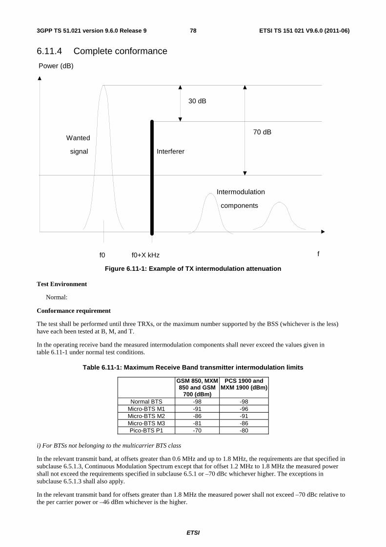
ETSI
ETSI TS 151 021 V9.6.0 (2011-06)783GPP TS 51.021 version 9.6.0 Release 9
6.11.4 Complete conformance
f0 f0+X kHz f
Power (dB)
30 dB
70 dBWanted
signal
Intermodulation
components
Interferer
Figure 6.11-1: Example of TX intermodulation attenuation
Test Environment
Normal:
Conformance requirement
The test shall be performed until three TRXs, or the maximum number supported by the BSS (whichever is the less) have each been tested at B, M, and T.
In the operating receive band the measured intermodulation components shall never exceed the values given in table 6.11-1 under normal test conditions.
Table 6.11-1: Maximum Receive Band transmitter intermodulation limits
GSM 850, MXM 850 and GSM
700 (dBm)
PCS 1900 and MXM 1900 (dBm)
Normal BTS -98 -98 Micro-BTS M1 -91 -96 Micro-BTS M2 -86 -91 Micro-BTS M3 -81 -86 Pico-BTS P1 -70 -80
i) For BTSs not belonging to the multicarrier BTS class
In the relevant transmit band, at offsets greater than 0.6 MHz and up to 1.8 MHz, the requirements are that specified in subclause 6.5.1.3, Continuous Modulation Spectrum except that for offset 1.2 MHz to 1.8 MHz the measured power shall not exceed the requirements specified in subclause 6.5.1 or –70 dBc whichever higher. The exceptions in subclause 6.5.1.3 shall also apply.
In the relevant transmit band for offsets greater than 1.8 MHz the measured power shall not exceed –70 dBc relative to the per carrier power or –46 dBm whichever is the higher.

ETSI
ETSI TS 151 021 V9.6.0 (2011-06)793GPP TS 51.021 version 9.6.0 Release 9
ii) For BTSs belonging to the multicarrier BTS class
In the relevant transmit band, at offsets from the wanted signal carrier frequency by more than 6 MHz and up to the edge of the relevant transmit band, the measured intermodulation products in a band of 600 kHz centered at their centre frequencies shall not exceed -36 dBm if maximum output power per carrier exceeds 33 dBm else -41 dBm, or -70 dBc, whichever less stringent. In addition, the measured third order intermodulation products may increase up to -60 dBc or -36 dBm, whichever is less stringent.
In the relevant transmit band, at offsets of less than or equal to 6 MHz, the requirements are that specified in 6.5.1.3, except that the measured intermodulation products shall not exceed -36 dBm if maximum output power per carrier exceeds 33 dBm else -41 dBm, or -70 dBc, whichever less stringent. In addition, the measured third order intermodulation products may increase up to -60 dBc or -36 dBm, whichever is less stringent.
In case of multicarrier BTS operating with one carrier, the level and number of allowable exceptions up to 10 MHz outside the relevant transmit band as defined in section 6.12.3 using N= 1 apply.
The intermodulation products shall never exceed -16 dBm, measured in 100 kHz bandwidth.
6.11.5 Requirement reference
3GPP TS 45.005 subclause 4.7.1.
6.12 Wideband noise and intra BSS intermodulation attenuation in multicarrier operation
6.12.1 Test purpose
To verify that the level of wideband noise and intermodulation products produced inside the relevant TX bands for a BTS belonging to the multicarrier BTS class do not exceed the specified limit when multiple carriers are active. The test is not applicable for MXM 850 and MXM 1900.
6.12.2 Test case
If SFH is supported by the BSS, it shall be disabled during this measurement.
a) The tests shall be performed per antenna connector for the declared maximum number of carriers transmitting on equal maximum power according to the power declaration. In addition the test shall be performed for the test case with unequal power distribution according to subclause 4.10.10 for the declared maximum number of carriers. The equipment shall be operated at equal and minimum frequency spacing specified for the BSS configuration under test. The test is performed for carriers located around M.
b) The multicarrier BTS shall be configured to operate with the lowest supported numbers of carriers (≥ 2) and the declared maximum number of carriers transmitting on equal maximum power according to the power declaration for each configuration and distributed as described below over the corresponding declared maximum Base Station RF bandwidth, configured to include B. The test is repeated in a configuration where maximum Base Station RF bandwidth includes T. In addition, if no third order intermodulation product at any of these configurations occurs within the relevant TX band or the maximum Transmit Filter bandwidth, whichever is smallest, the carrier frequency spacings shall be equally reduced until one of the third order intermodulation product closest to the group of carriers occurs on one of the band edges of the applicable bandwidth, and the test is repeated. When reducing the spacings, both carrier frequency configurations shall be tested: one where the lowest frequency is kept at B and as close as possible to the lower band edge and one where the highest frequency is kept at T and as close as possible to the upper band edge of the relevant transmit band.
c) If the multicarrier BTS equipment according to the vendor declaration supports non-contiguous frequency allocation as defined in subclause 4.10.10 and four or more carriers, tests shall be performed per antenna connector with two pairs of carriers, located around M with 5.4 MHz separation between the innermost carriers of the pairs and minimum frequency spacing within the pairs. The carriers shall be operating at equal declared maximum power for this configuration.

ETSI
ETSI TS 151 021 V9.6.0 (2011-06)803GPP TS 51.021 version 9.6.0 Release 9
To distribute the carriers in test case b) the difference between adjacent carrier spacings between the carrier center frequencies shall be maximum ±200kHz and the third order IM products, generated by any combination of two or three frequencies, shall coincide within 400 kHz, measured at the center frequencies of the IM products. Any combination fulfilling these criteria can be used, but the same carrier frequency configuration shall be used when B or T respectively is included in the measurement. The following procedure applies:
1 Calculate the maximum possible equal frequency spacing (Deq) within the declared maximum Base Station RF bandwidth (RF-BWmax). Note that the center frequencies of the outermost carriers shall be 200 kHz inside the band edges of RF-BWmax.
2 Allocate one carrier at lowest and one at highest frequency possible within the RF-BWmax.
3 Allocate the remaining carriers at frequencies shifted from one of the outermost carriers by a multiple of Deq with altering offsets. These offsets may be chosen freely to be either 0, + 200 kHz or - 200 kHz but the difference between two adjacent spacings shall be no more than 200 kHz. It is not allowed to set all offsets to 0. In addition the IM spread limits (IM3 to coincide within 400 kHz) shall be fulfilled.
For frequency offsets from the centre frequency of the uppermost and lowermost active carrier of more than 6 MHz the average power shall be measured over sufficient time slots to ensure conformance according to methodology of annex A.1.
- Within a 600 kHz band centered at the centre frequencies of the intermodulation components the measurements shall be performed with the center frequencies of the measurement bandwidth in the frequency band ± 150 kHz around the centre frequencies of the intermodulation components, using a measurement bandwidth of 300 kHz. The reference power for relative measurements shall be the power measured in a bandwidth of 300 kHz for one of the carriers under test.
- For offsets outside the 600 kHz bands around the centre frequencies of the intermodulation components, the measurements shall be performed with the center frequencies of the measurement bandwidth starting at ± 350 kHz around the centre frequencies of the intermodulation components, using a measurement bandwidth of 100 kHz. The reference power for relative measurements in a bandwidth of 30 kHz for one of the carriers under test.
For frequency offsets from the centre frequency of the uppermost and lowermost active carrier of1.8 MHz up to and including 6 MHz the average power shall be measured in a frequency scan mode, with a minimum sweep time of 75 ms and averaged over 200 sweeps.
- Within a 600 kHz band centered at the centre frequencies of the intermodulation components , the measurements shall be performed with the center frequencies of the measurement bandwidth in the frequency band ± 250 kHz around the centre frequencies of the intermodulation components, using a RF and video filter bandwidth of the measuring instrument of 100 kHz. The reference power for relative measurements shall be the power measured in a bandwidth of 100 kHz for one of the carriers under test.
- For offsets outside the 600 kHz bands around the centre frequencies of the intermodulation components, the measurements shall be performed with the center frequencies of the measurement bandwidth starting at ± 350 kHz around the centre frequencies of the intermodulation components, using a measurement bandwidth of 100 kHz. The reference power for relative measurements shall be the power measured in a bandwidth of 30 kHz for one of the carriers under test.
For frequency offsets from the centre frequency of the uppermost and lowermost active carrier of less than 1.8 MHz the average power shall be measured selectively using video averaging over 50 to 90 % of the useful part of the time slot excluding the mid-amble. The averaging shall be over at least 200 time slots and only active bursts shall be included in the averaging process. The RF and video filter bandwidth of the measuring instrument shall be 30 kHz. The reference power for relative measurements shall be the power measured in a bandwidth of 30 kHz for one of the carriers under test.
The measurement conditions for the Continuous Modulation Spectrum regarding frequency offsets and detector settings shall be the same as defined in subclause 6.5.1 for multicarrier BTS.
ETSI
ETSI TS 151 021 V9.6.0 (2011-06)813GPP TS 51.021 version 9.6.0 Release 9
6.12.3 Essential conformance
Test Environment
Normal:
Conformance requirement
For multicarrier BTS when more than one carrier is active, in the relevant transmit band, the unwanted emission power shall be measured at offsets between 0.4 MHz from the uppermost and lowermost wanted signal carrier frequency and 10 MHz outside the edge of the relevant transmit band.
At frequency offsets higher than or equal to 1.8 MHz from the centre frequency of the uppermost and lowermost active carrier up to 10 MHz outside the edge of the relevant transmit band, the unwanted emission for the multicarrier BTS shall not exceed the less stringent of the following requirements:
- in a frequency band of 600 kHz centered at the centre frequencies of the intermodulation components, the average power measured over a timeslot shall not exceed -70 dBc or -36 dBm if maximum output power per carrier exceeds 33 dBm else -41 dBm, whichever is less stringent, .
- in addition, in a frequency band of 600 kHz centered at the third order intermodulation centre frequencies, the average power of the measured intermodulation components over a timeslot may increase up to -60 dBc.
- the requirements specified in subclause 6.5.1, Continuous Modulation Spectrum, increased by 10*LOG(N) dB where N is the number of active carriers.
In order to prove the compliance with the intermodulation requirements, the power of all third and fifth order intermodulation products shall be measured.
In the test case with unequal power distribution, the reference for the relative requirements is the power of the carrier with the highest power is applied.
At frequency offsets of less than 1.8 MHz from the outermost carriers, the unwanted emissions must fulfil a mask that is defined in the following steps:
1. The dBc values of table 6.5-1 in subclause 6.5.1 (Aj with j=1 to N) are extracted for each carrier, taking into account the output power level of one carrier and the corresponding frequency offset between the measurement frequency point and the respective carrier. For carriers at offsets above 1.8 MHz from the measurement frequency point, the dBc value for the respective carrier must be reduced by 5 dB to account for the bandwidth conversion from 100 kHz to 30 kHz.
2. The dBc value (Aj with j=N+1) of the IM attenuation defined in sub-clause 6.12 for the multicarrier BTS class has to be derived. In some configurations there might be no IM product falling onto the respective frequency. Then this contribution is ignored in the following.
3. The obtained N+1 dBc values are cumulated in the (following way) linear domain:
∑+
=
=1
1
10/10, 10log10
N
j
AdBcCumulated
jA .
4. This procedure has to be done for the following frequency offsets above the uppermost and below the lowermost carriers: 400 kHz, 600 kHz, 1200 kHz and 1800 kHz.
5. For each of these measurement frequency points, the measured spectrum must not exceed the respective unwanted emission mask defined by Acumulated, dBc.
For test case c) the requirements above the uppermost carrier and below the lowermost carrier are the same as specified above with N being the total number of active carriers. In addition the test includes the measurement of the frequency range between the innermost carriers of the two pairs of carriers, where the following requirements apply:
- For frequency offsets of less than 1.8 MHz above the centre frequency of the uppermost carrier A of the lower pair of carriers or below the centre frequency of the lowermost carrier B of the upper pair of carriers, the unwanted emission must not exceed a mask defined by the cumulation of the spectrum due to modulation and wideband noise from each of the N carriers and the IM products,

ETSI
ETSI TS 151 021 V9.6.0 (2011-06)823GPP TS 51.021 version 9.6.0 Release 9
as specified above in this subclause for frequency offsets of less than 1.8 MHz for the test of contiguous carrier allocations.
- For frequency offsets of 1.8 MHz, 2.0 MHz, 2.2 MHz, 2.4 MHz and 2.6 MHz above the centre frequency of the uppermost carrier A of the lower pair of carriers: the value of the spectrum due to modulation and wideband noise given for the measurement of carrier A may not increase by more than 10*LOG (N) dB, or fulfil the requirement given above for the multicarrier BTS class, whichever is the less stringent.
- For frequency offsets of 1.8 MHz 2.0 MHz, 2.2 MHz, 2.4 MHz and 2.6 MHz below the centre frequency of the lowermost carrier B of the upper pair of carriers: the value of the spectrum due to modulation and wideband noise given for the measurement of carrier B may not increase by more than 10*LOG (N) dB, or fulfil the requirement given above for the amulticarrier BTS class, whichever is the less stringent.
The absolute lower limit in item 6) in subclause 6.5.1.3 shall apply for all numbers N of active carriers.
At offsets between 600 kHz above the uppermost and below the lowermost carrier, respectively, and 10 MHz outside the relevant transmit band, in bands of 200 kHz width centered on a frequency, which is an integer multiple of 200 kHz, in test case a) and b) exceptions are allowed for N active carriers at M= 18 + 3* (N-1) or up to 40 bands, whichever the lowest. All exceptions are measured in 100 kHz bandwidth, averaged over the 200 kHz band and may be up to –36 dBm. In addition, all exceptions within the relevant transmit band and up to four exceptions at offsets up to 2 MHz from the respective band edges, may be up to -70 dBc relative to the carrier measured in a bandwidth of 100 kHz, or -36 dBm, whichever less stringent. For test case c) the same total number of exceptions M for N active carriers shall apply as given above for test case a) , including the range of frequency offsets between 0.6 MHz above the uppermost carrier of the lower pair of carriers and 0.6 MHz below the lowermost carrier of the upper pair of carriers. Such bands, which centre frequency coincides with the centre frequency of third order IM products of any combination of two or three active carriers and corresponding adjacent channels (±200 kHz), shall not be included in counting the exceptions.
6.12.4 Complete conformance
The requirement of essential conformance shall apply.
6.12.5 Requirement reference
3GPP TS 45.005 subclauses 4.2.1 and 4.7.2.
7 Receivers All tests unless otherwise stated in this subclause shall be conducted on Base Station Systems fitted with a full complement of Transceivers for the configuration. The manufacturer shall provide appropriate logical or physical test access to perform all tests in this subclause. Measurements shall include any RX multicoupler.
The tests in this subclause assume that the receiver is not equipped with diversity. For receivers with diversity, the tests may be performed by applying the specified signals to one of the receiver inputs, and terminating or disabling the other(s). The tests and requirements are otherwise unchanged.
For receivers with diversity, testing of essential conformance shall be performed by applying the specified signals to one of the receiver inputs, and terminating or disabling the other(s). This does not apply to cases which are specified for two antenna configuration only, i.e. EGPRS2-B with higher symbol rate and channels in VAMOS mode. In this case all receiver tests are performed in two antenna configuration except in Static propagation conditions. At two-antenna configuration the requirements are specified for no correlation or gain imbalance between the two receive branches.
The Rx performance requirements for modulation schemes using higher symbol rate are based on input signals using the wide pulse shaping filter unless otherwise stated. For definition of narrow and wide pulse-shaping filters, see 3GPP TS 45.004 [21]. The input signals used are defined by
Narrow pulse-shaping filter: Higher symbol rate using spectrally narrow pulse shaping filter.
Wide pulse-shaping filter: Higher symbol rate using spectrally wide pulse shaping filter.

ETSI
ETSI TS 151 021 V9.6.0 (2011-06)833GPP TS 51.021 version 9.6.0 Release 9
For multicarrier BTS the test cases and requirements for normal BTS apply unless otherwise stated for multicarrier receiver. The BTS configuration conditions in subclause 4.10.10 apply.
Requirements do not apply to channels in VAMOS mode unless explicitly stated. When they apply, they shall apply to both VAMOS sub-channels. VAMOS sub-channel 1 shall use TSC-5 from TSC Set 1 and VAMOS sub-channel 2 shall use TSC-5 from TSC Set 2.
In all the relevant subclauses in this clause all Bit Error Ratio (BER), Residual BER (RBER), Block error Ratio (BLER) and Frame Erasure Ratio (FER) measurements shall be carried out according to the general rules for statistical testing in annex A.
7.1 Static Layer 1 receiver functions (nominal error ratios)
7.1.1 Test Purpose
The static Layer 1 receiver functions verified in these tests are the RF parts, the multiplexing and multiple access functions, any existing equalizer, the deciphering functions, the de-interleaving and the channel decoding on the receive side. The performance of the receiver at the maximum specified input level is also verified.
Nominal error ratios (Bit Error Ratio - BER) are measured at a logical reference point that represents the performance before channel decoding. This measurement can be performed for TCH/FS, using unprotected class II bits extracted after channel decoding, but before any extrapolation. Therefore, the results obtained are representative of the logical reference point before channel decoding. The test can also be performed on the uncoded bits extracted before any channel decoding of a PDTCH channel.
If the BTS supports SFH, this test also verifies the TCH/FS performance in frequency hopping under interference conditions. In this case, the Frame Erasure Ratio (FER) for TCH/FS is used as the performance criteria.
The Random access performance at high input levels is verified by measuring the Frame Erasure Ratio for RACH.
7.1.2 Test Case
GMSK modulation
1) For BER measurements, if Slow Frequency Hopping (SFH) is supported by the BSS, the BSS shall be hopping over the maximum range and number of ARFCNs possible for the test environment and which are available in the BSS configuration. If SFH is not supported, the test shall be performed for the radio frequency channels B, M and T. In both cases the tests shall be repeated until all the RF equipment in the BSS configuration is tested on all specified carrier frequencies.
If test is performed with TCH/FS a test signal with normal TCH/FS modulation originating from the BSSTE shall be applied to the BSS receiver input. The unprotected class II bits obtained from the BSS receiver after channel decoding and before any extrapolation shall be compared with the unprotected class II bits originating from the BSSTE.
If test is not performed with TCH/FS a test signal with normal PDTCH modulation originating from the BSSTE shall be applied to the BSS receiver input. The uncoded data bits obtained from the BSS receiver shall be compared with the bits originating from the BSSTE.
NOTE: Uncoded data bits refer to the encrypted bits of a burst, extracted by the receiver without any signal processing improvement from encoding/decoding of the signal.
The test shall be performed at the following power levels of test signal:
a) A lower limit (20 dB above the reference sensitivity level of the BSS under test), as specified in table 7.1-1, for static propagation conditions.
b) -40 dBm, for static propagation conditions.
c) -15 dBm for GSM 400, GSM 700, GSM900, GSM850 and MXM 850 BTS, -18 dBm for GSM 400, T-GSM 810, GSM850 and E-GSM 900 multicarrier BTS equipped with multicarrier receiver, and -23 dBm for DCS1800, PCS 1900 and MXM 1900, for static propagation conditions only.

ETSI
ETSI TS 151 021 V9.6.0 (2011-06)843GPP TS 51.021 version 9.6.0 Release 9
d) -5 dBm for GSM900, GSM 700, GSM850 and MXM 850 pico-BTS and -14 dBm for DCS1800, PCS 1900 and MXM 1900 pico-BTS, for static propagation conditions only.
e) A lower limit (20 dB above the reference sensitivity level of the BSS under test), as specified in table 7.1-1, for EQ50 propagation conditions, except for GSM 400 where EQ100 applies and for GSM 700 where EQ60 applies, step e) does not apply to pico-BTS.
f) -40dBm, for EQ50 propagation conditions, except for GSM 400 where EQ100 applies and for GSM 700 where EQ60 applies, step f) does not apply to pico-BTS.
2) For RACH, the test shall be performed for the radio frequency channels B, M and T. A test signal consisting of RACH bursts originating from the BSSTE shall be applied to the BSS receiver input. The proportion of RACH bursts at the input to the receiver which are not correctly identified by the BSS shall be measured.
The test shall be performed at the following power levels of test signal:
a) A lower limit (20 dB above the reference sensitivity level of the BSS under test), as specified in table 7.1-1, for static propagation conditions.
b) -40 dBm, for static propagation conditions.
c) -15 dBm for GSM 400, GSM 700, GSM900, GSM850 and MXM 850BTS, -16 dBm for GSM 400, T-GSM 810, GSM850 and E-GSM 900 multicarrier BTS equipped with multicarrier receiver, and -23 dBm for DCS1800, PCS 1900 and MXM 1900 for static propagation conditions.
3) For TCH/FS FER measurements in frequency hopping under interference conditions, two signals are connected to the BSS receiver input via a combining network. The wanted signal with an RF level given in table 7.1-1 shall be cyclically frequency hopping on four carrier frequencies under static conditions. The interfering signal shall be a random continuous, GMSK-modulated signal on only one of the carriers at a level 10 dB higher than the wanted signal. The test shall be performed with the hopping frequencies centered around RF channel M.
8-PSK, QPSK, 16-QAM and 32-QAM modulations
1) If Slow Frequency Hopping (SFH) is supported by the BSS, the BSS shall be hopping over the maximum range and number of ARFCNs possible for the test environment and which are available in the BSS configuration. If SFH is not supported, the test shall be performed for the radio frequency channels B, M and T. In either case the tests shall be repeated until all the RF equipment in the BSS configuration is tested on all specified carrier frequencies.
A test signal with normal PDTCH modulation originating from the BSSTE shall be applied to the BSS receiver input. The uncoded data bits obtained from the BSS receiver shall be compared with the bits originating from the BSSTE.
NOTE: Uncoded data bits refer to the encrypted bits of a burst, extracted by the receiver without any signal processing improvement from encoding/decoding of the signal.
The test shall be performed at the following power levels of test signal:
a) A lower limit level, as specified in table 7.1-1, for static propagation conditions.
b) –40dBm, for static propagation conditions.
c) The maximum limit as specified in table 7.1-1, for static propagation conditions.
d) Step a and b shall be repeated with the frequency of the input 8-PSK and, if supported, QPSK, modulated signal randomly offset, by +-0,1 ppm (except +-0,2 ppm for GSM400), on a burst-by-burst basis. For each burst, the sign of the frequency offset is chosen according to a 511-bit pseudo-random sequence, defined in ITU-T recommendation O.153.

ETSI
ETSI TS 151 021 V9.6.0 (2011-06)853GPP TS 51.021 version 9.6.0 Release 9
Table 7.1-1: Limit of RF input for testing of Static Layer 1 receiver functions
BTS Type Lower Limit
GMSK, 8-PSK and
QPSK
Maximum Limit
8-PSK and QPSK
Lower Limit 16-QAM and 32-QAM
EGPRS2-A
Lower Limit 16-QAM and 32-QAM
EGPRS2-B
Maximum Limit 16-QAM and 32-QAM
GSM 400/GSM850/GSM900/DCS1800/PCS 1900/MXM 850/MXM 1900/GSM 700 BTS
-84 dBm -26 dBm -84 -78 -29
GSM900/GSM850/MXM 850/GSM 700 micro-BTS M1
-77 dBm -24 dBm -77 -71 -27
GSM900/GSM850/MXM 850/GSM 700 micro-BTS M2
-72 dBm -19 dBm -72 -66 -22
GSM900/GSM850/MXM 850/GSM 700 micro-BTS M3
-67 dBm -14 dBm -67 -61 -17
GSM900/GSM850/MXM 850/GSM 700 pico-BTS P1
-68 dBm -16 dBm -68 -62 -19
DCS1800/PCS 1900/ MXM 1900 micro-BTS M1 -82 dBm -24 dBm -82 -76 -27 DCS1800/PCS 1900/ MXM 1900 micro-BTS M2 -77 dBm -19 dBm -77 -71 -22 DCS1800/PCS 1900/ MXM 1900 micro-BTS M3 -72 dBm -14 dBm -72 -66 -17 DCS1800/PCS 1900/ MXM 1900 pico-BTS P1 -75 dBm -17 dBm -75 -69 -20
7.1.3 Essential conformance
This test need not be performed.
7.1.4 Complete conformance
Test Environment:
Normal: For GMSK BER measurements, each TRX shall be tested.
For RACH, the TRX supporting the BCCH shall be tested.
For 8-PSK, QPSK, 16-QAM and 32-QAM modulation, each TRX shall be tested. Any modulated channel type for each modulation can be used.
Extreme Temperature: For GMSK BER measurements, one TRX shall be tested on one timeslot, for static propagation conditions only.
For RACH, the TRX supporting the BCCH shall be tested.
For TCH/FS FER measurements, the test need not be performed.
For 8-PSK, QPSK, 16-QAM and 32-QAM modulation, one TRX shall be tested on one timeslot, for static propagation conditions only. Any modulated channel type for each modulation can be used.
Vibration: For GMSK BER measurements, one TRX shall be tested on one timeslot, for static propagation conditions only.
For TCH/FS FER measurements in frequency hopping under interference conditions and for RACH, the test need not be performed.
For 8-PSK, QPSK, 16-QAM and 32-QAM modulation, one TRX shall be tested on one timeslot, for static propagation conditions only. Any modulated channel type for each modulation can be used.
For multicarrier BTS with multicarrier receiver the tests above shall be tested for each receiver antenna port.
Conformance Requirement
The bit error ratio of the unprotected bits (TCH/FS, Class II or uncoded PDTCH bits) shall not exceed:
Static propagation conditions BER ≤ 10-4 For input levels up to -40 dBm

ETSI
ETSI TS 151 021 V9.6.0 (2011-06)863GPP TS 51.021 version 9.6.0 Release 9
Static propagation conditions BER ≤ 10-3 For input levels > -40 dBm
EQ50 (except for GSM400, where EQ100 applies) propagation conditions BER ≤ 3 %
The FER of TCH/FS under interfering conditions shall not exceed 5 %.
The frame erasure ratio of the RACH shall not exceed 0.5%.
The bit error ratio of uncoded data bits in 8-PSK, QPSK, 16-QAM and 32-QAM channels shall not exceed:
Static propagation conditions (steps a, b and d) BER ≤ 10-4 for input levels up to -40 dBm.
Static propagation conditions (step c) BER ≤ 10-3 for input levels > -40 dBm.
7.1.5 Requirement Reference
3GPP TS 45.005 subclause 6.1, subclause 6.5 and subclause 6.6.
7.2 Erroneous Frame Indication Performance
7.2.1 Test Purpose
In 3GPP TS 45.005 a Cyclic Redundancy Check (CRC) is defined for detection of erroneous Layer 2 frames or speech frames. For speech channels also additional error detecting capabilities using some soft information are needed due to DTX operation when no useful signal is transmitted to the receiver. This test verifies the reliability of the overall Bad Frame Indication (BFI) presented to the speech decoder and the Frame Erasure Indication (FEI) used on control channels.
7.2.2 Test Case
1) A test signal consisting of continuous GSM modulation of a pseudo random bit stream without mid-amble, and at a level specified in table 7.2-1, shall be applied to the receiver antenna connector, on the same frequency as the TRX under test.
One TRX shall be configured to support a BCCH. The detection by the BSS of error-free RACH bursts (FEI=0) shall be monitored by the BSSTE. If both GPRS is supported by the BSS and a PBCCH can be configured, then the detection by the BSS of error-free PRACH bursts (FEI=0) shall be monitored by the BSS.
Table 7.2-1: Test Signal input level for testing of Erroneous Frame Indication performance
BTS Type Test signal Input Level GSM 400/GSM850/GSM900/DCS1800/PCS 1900/MXM 850/MXM 1900/GSM 700 BTS
-84 dBm
GSM900/GSM850/MXM 850/GSM 700 micro-BTS M1 -77 dBm GSM900/GSM850/MXM 850/GSM 700 micro-BTS M2 -72 dBm GSM900/GSM850/MXM 850/GSM 700 micro-BTS M3 -67 dBm GSM900/GSM850/MXM 850/GSM 700 pico-BTS P1 -68 dBm DCS1800/PCS 1900/ MXM 1900 micro-BTS M1 -82 dBm DCS1800/PCS 1900/ MXM 1900 micro-BTS M2 -77 dBm DCS1800/PCS 1900/ MXM 1900 micro-BTS M3 -72 dBm DCS1800/PCS 1900/ MXM 1900 pico-BTS P1 -75 dBm
2) Step 1 shall be repeated without any RF input on the TRX under test, with the receiver antenna connector
terminated with 50Ω.
3) Step 1 shall be repeated with one timeslot on one TRX configured for TCH/FS, TCH/HS, TCH/EFS, TCH/AxS and for FACCH. The Bad Frame Indication (BFI) shall be monitored by the BSSTE.
4) Step 3 shall be repeated without any RF input on the TRX under test, with the receiver antenna connector terminated with 50Ω.

ETSI
ETSI TS 151 021 V9.6.0 (2011-06)873GPP TS 51.021 version 9.6.0 Release 9
5) The test shall be repeated with one timeslot on one TRX configured for TCH/FS, TCH/HS, TCH/EFS and TCH/AxS, when DTX is activated with SID frames and SACCH frames received at a level specified in table 7.2-1 and with no transmission at the other bursts of the TCH. The Bad Frame Indication (BFI) shall be monitored by the BSSTE.
7.2.3 Essential conformance
This test need not be performed.
7.2.4 Complete conformance
Test Environment:
Normal.
Conformance requirement
In steps 1 and 2, less than 0.02 % of the frames shall be detected as error free (FEI=0).
In steps 3, 4 and 5, less than 1 undetected bad speech frame (i.e. detected as BFI=0) shall occur on average in a period of 60 s.
7.2.5 Requirement reference
3GPP TS 45.005 subclause 6.4.
7.3 Static Reference Sensitivity Level
7.3.1 Test Purpose
The static reference sensitivity level of the receiver is the level of signal at the receiver input with a standard test signal at which the receiver will produce after demodulation and channel decoding data with a Frame Erasure Ratio (FER), Residual Bit Error Ratio (RBER) Bit Error Ratio (BER) or Block Error Ratio (BLER) better than or equal to that specified for a specific logical channel type under static propagation conditions.
7.3.2 Test Case
The test shall be performed for the specified ARFCNs. As a minimum, one time slot shall be tested on one TRX.
All TRXs in the BSS configuration shall be on and transmitting full power in all time slots.
For circuit switched channels, except ECSD with slow frequency hopping disabled and AMR-WB, and 8-PSK modulated AMR and AMR-WB channels, a test signal with normal GSM modulation shall be applied to the BSS RX antenna connector, with a power specified in table 7.3-1, on a chosen time slot.
For packet switched channels, for ECSD with slow frequency hopping disabled and AMR-WB, and 8-PSK modulated AMR and AMR-WB channels, a test signal with normal GSM modulation shall be applied to the BSS RX antenna connector, with a power specified in table 7.3-2, on a chosen time slot. When testing the packet switched channels with PAN included the input signal power specified in tables 7.3-3 and 7.3-4 shall be applied.
For BTS types other than normal, the test signal input level shall be increased by the values in table 7.3-5.
The two adjacent time slots shall have a level 50 dB above reference sensitivity requirement specified in table 7.3-1. The content of this signal shall allow the receiver of the TRX under test to either be activated or to detect valid GMSK modulated GSM signals (as specified in the conformance requirement) on the adjacent timeslots for the duration of the test. No signal should be applied during the remaining timeslots.
If Synthesizer Slow Frequency Hopping is supported by the BSS, the test shall be repeated with the following changes:

ETSI
ETSI TS 151 021 V9.6.0 (2011-06)883GPP TS 51.021 version 9.6.0 Release 9
a) The BSS shall be hopping over the maximum range and number of ARFCNs possible for the test environment and which are available in the BSS configuration.
b) The test signal should only be applied for the timeslot under test; no signal should be applied during the remaining timeslots.
Table 7.3-1: Test Signal input level for Static reference sensitivity measurement for circuit switched channels except ECSD and AMR-WB channels, and 8-PSK modulated AMR and AMR-WB channels
BTS Type Test signal Input Level GMSK
GSM 400/GSM850/GSM900/DCS1800/PCS 1900/MXM 850/MXM 1900/GSM 700 BTS
-104 dBm
GSM900/GSM850/MXM 850/GSM 700 micro-BTS M1 -97 dBm GSM900/GSM850/MXM 850/GSM 700 micro-BTS M2 -92 dBm GSM900/GSM850/MXM 850/GSM 700 micro-BTS M3 -87 dBm GSM900/GSM850/MXM 850/GSM 700 pico-BTS P1 -88 dBm
DCS1800/PCS 1900/ MXM 1900 micro-BTS M1 -102 dBm DCS1800/PCS 1900/ MXM 1900 micro-BTS M2 -97 dBm DCS1800/PCS 1900/ MXM 1900 micro-BTS M3 -92 dBm DCS1800/PCS 1900/ MXM 1900 pico-BTS P1 -95 dBm

ETSI
ETSI TS 151 021 V9.6.0 (2011-06)893GPP TS 51.021 version 9.6.0 Release 9
Table 7.3-2: Test Signal input level for Static reference sensitivity measurement for packet switched channels without PAN, ECSD and AMR-WB channels, and 8-PSK modulated AMR and AMR-WB
channels
Normal BTS (GSM400, GSM850, GSM900, DCS1800, PCS1900, GSM 700, MXM850* , MXM1900*) Type of Channel Static TTI (2) Comment
PDTCH/CS-1 to 3 dBm -104 BTTI PDTCH/CS-4 dBm -101 BTTI PRACH/11 bits dBm -104 - PRACH/8 bits dBm -104 - PACCH dBm -104 - PDTCH/MCS-1 dBm -104 BTTI & RTTI PDTCH/MCS-2 dBm -104 BTTI & RTTI PDTCH/MCS-3 dBm -104 BTTI & RTTI PDTCH/MCS-4 dBm -101.5 BTTI & RTTI PDTCH/MCS-5 dBm -101 BTTI & RTTI PDTCH/MCS-6 dBm -99.5 BTTI & RTTI PDTCH/MCS-7 dBm -96 BTTI & RTTI PDTCH/MCS-8 dBm -93 BTTI & RTTI PDTCH/MCS-9 dBm -91.5 BTTI & RTTI PDTCH/UAS-7 dBm -97.5 BTTI & RTTI PDTCH/UAS-8 dBm -96.5 BTTI & RTTI PDTCH/UAS-9 dBm -96 BTTI & RTTI PDTCH/UAS-10 dBm -95 BTTI & RTTI PDTCH/UAS-11 dBm -93 BTTI & RTTI PDTCH/UBS-5 dBm -103.5 BTTI & RTTI Input signal
generated with narrow
pulse-shaping filter
PDTCH/UBS-6 dBm -101.5 BTTI & RTTI PDTCH/UBS-7 dBm -95 BTTI & RTTI PDTCH/UBS-8 dBm -93 BTTI & RTTI PDTCH/UBS-9 dBm -91.5 BTTI & RTTI PDTCH/UBS-10 dBm -88 BTTI & RTTI PDTCH/UBS-11 dBm -85.5 BTTI & RTTI PDTCH/UBS-12 dBm -84.5 BTTI & RTTI PDTCH/UBS-5 dBm -104 BTTI & RTTI Input signal
generated with wide
pulse-shaping filter
PDTCH/UBS-6 dBm -104 BTTI & RTTI PDTCH/UBS-7 dBm -101 BTTI & RTTI PDTCH/UBS-8 dBm -99.5 BTTI & RTTI PDTCH/UBS-9 dBm -98.5 BTTI & RTTI PDTCH/UBS-10 dBm -95 BTTI & RTTI PDTCH/UBS-11 dBm -93 BTTI & RTTI PDTCH/UBS-12 dBm -91.5 BTTI & RTTI E-FACCH/F dBm -104 E-TCH/F43.2 (NT) dBm -97 E-TCH/F32 (T) dBm -104 E-TCH/F28.8 (T) dBm -99.5 E-TCH/F28.8 (NT) dBm -100 TCH/WFS12.65 dBm -104 TCH/ WFS8.85 dBm -104 TCH/WFS6.60 dBm -104 O-FACCH/F dBm -104 O-FACCH/H dBm -104 O-TCH/AHS12.2 dBm -100,5 O-TCH/AHS10.2 dBm -101 O-TCH/AHS7.95 dBm -102,5 O-TCH/AHS7.4 dBm -102,5 O-TCH/AHS6.7 dBm -103 O-TCH/AHS5.9 dBm -103,5 O-TCH/AHS5.15 dBm -104 O-TCH/AHS4.75 dBm -104 O-TCH/AHS-INB (FER) dBm -103,5 O-TCH/AHS (EVSIDUR) dBm -104

ETSI
ETSI TS 151 021 V9.6.0 (2011-06)903GPP TS 51.021 version 9.6.0 Release 9
O-TCH/AHS (EVRFR) dBm -104 O-TCH/WFS23.85 dBm -100,5 O-TCH/WFS15.85 dBm -102,5 O-TCH/WFS12.65 dBm -104 O-TCH/WFS8.85 dBm -104 O-TCH/WFS6.60 dBm -104 O-TCH/WFS-INB (FER) dBm -104 O-TCH/WFS (EVSIDUR) dBm -104 O-TCH/WFS (EVRFR) dBm -104 O-TCH/WHS12.65 dBm -100,5 O-TCH/WHS8.85 dBm -102,5 O-TCH/WHS6.60 dBm -103 O-TCH/WHS-INB (FER) dBm -103,5 O-TCH/WHS (EVSIDUR) dBm -104 O-TCH/WHS (EVRFR) dBm -104 *NOTE 1: PDTCH/CS-1 to 4 and ECSD are not applicable for MXM850 and MXM1900 NOTE 2: Test Signal input levels for Static reference sensitivity apply to BTTI without PAN as well as
RTTI without PAN for PDTCH indicated in the table. NOTE 3: The requirements for all channel types assume single antenna configuration.
Table 7.3-3: Test Signal input level for Static reference sensitivity measurement for packet switched channels with PAN included
Normal BTS (GSM400, GSM850, GSM900, DCS1800, PCS1900, GSM 700, MXM850* , MXM1900*) Type of Channel Static TTI (1) Comment
PDTCH/MCS-1 dBm -104 BTTI & RTTI PDTCH/MCS-2 dBm -104 BTTI & RTTI PDTCH/MCS-3 dBm -104 BTTI & RTTI PDTCH/MCS-5 dBm -101 BTTI & RTTI PDTCH/MCS-6 dBm -99.5 BTTI & RTTI PDTCH/MCS-7 dBm -96 BTTI & RTTI PDTCH/MCS-8 dBm -93 BTTI & RTTI PDTCH/UAS-7 dBm -97 BTTI & RTTI PDTCH/UAS-8 dBm -96.5 BTTI & RTTI PDTCH/UAS-9 dBm -95.5 BTTI & RTTI PDTCH/UAS-10 dBm -94.5 BTTI & RTTI PDTCH/UAS-11 dBm -92.5 BTTI & RTTI PDTCH/UBS-5 dBm -104 BTTI & RTTI Input signal
generated with wide
pulse-shaping filter
PDTCH/UBS-6 dBm -104 BTTI & RTTI PDTCH/UBS-7 dBm -101 BTTI & RTTI PDTCH/UBS-8 dBm -99.5 BTTI & RTTI PDTCH/UBS-9 dBm -98.5 BTTI & RTTI PDTCH/UBS-10 dBm -95 BTTI & RTTI PDTCH/UBS-11 dBm -92 BTTI & RTTI PDTCH/UBS-12 dBm -89.5 BTTI & RTTI NOTE 1: Test Signal input levels for Static reference sensitivity apply to BTTI with PAN as well as
RTTI with PAN for PDTCH indicated in the table. NOTE 2: The requirements for all channel types assume single antenna configuration.

ETSI
ETSI TS 151 021 V9.6.0 (2011-06)913GPP TS 51.021 version 9.6.0 Release 9
Table 7.3-4: Test Signal input level for Static reference sensitivity measurement for PAN
Normal BTS (GSM400, GSM850, GSM 900, DCS 1800 & PCS 1900)
Type of Propagation condition Comment
channel Static
PDTCH/MCS-1 to 3 dBm -104
PDTCH/MCS-5 to 6 dBm -104
PDTCH/MCS-7 dBm -104
PDTCH/MCS-8 dBm -104
PDTCH/UAS-7 to 9 dBm -104
PDTCH/UAS-10 dBm -104
PDTCH/UAS-11 dBm -104
PDTCH/UBS-5 to 6 dBm -104 Input signal generated with wide
pulse-shaping filter
PDTCH/UBS-7 to 8 dBm -104
PDTCH/UBS-9 dBm -104
PDTCH/UBS-10 dBm -104
PDTCH/UBS-11 to 12 dBm -104 NOTE : The requirements for all channel types assume single antenna configuration and apply to
BTTI & RTTI.
Table 7.3-5: Test signal input level corrections for different BTS Types (for table 14b)
BTS Type Test signal Average Input Level corrections GSM400/GSM850/GSM900/MXM850/GSM 700 micro-BTS M1
+7 dB
GSM900/GSM850/MXM850/GSM 700 micro-BTS M2 +12 dB GSM900/GSM850/MXM850/GSM 700 micro-BTS M3 +17 dB GSM900/GSM850/MXM850/GSM 700 pico-BTS P1 +16 dB DCS1800/PCS 1900/ MXM 1900 micro-BTS M1 +2 dB DCS1800/PCS 1900/ MXM 1900 micro-BTS M2 +7 dB DCS1800/PCS 1900/ MXM 1900 micro-BTS M3 +12 dB DCS1800/PCS 1900/ MXM 1900 pico-BTS P1 +9 dB
The input signal before channel encoding in the BSSTE shall be compared with the signal which is obtained from the BSS receiver after channel decoding.
7.3.3 Essential conformance
Test Environment:
Normal.
Conformance Requirement
For tests with SFH disabled, the tests shall be performed at one ARFCN. For tests with SFH enabled, the tests shall be performed with the range of hopping frequencies centred around RF channel M.
The error performance given in table 7.3-6 shall be met for TCH/FS channel (FER and RBER for class Ib and class II bits) and TCH/HS channel (FER and RBER for class Ib and class II bits with BFI=0).
If GPRS is supported by the BSS, the error performance given in table 7.3-6 shall be met for PDTCH/CS-1 channel (BLER).
If AMR or AMR-WB is supported by the BSS, the error performance given in table 7.3-6 shall be met for one channel. The channel with the highest bitrate shall be tested.

ETSI
ETSI TS 151 021 V9.6.0 (2011-06)923GPP TS 51.021 version 9.6.0 Release 9
If 8-PSK modulated AMR or AMR-WB is supported by the BSS, the error performance given in table 7.3-6 shall be met for one traffic channel and corresponding associated control channel O-FACCH. The traffic channel with the highest bitrate shall be tested
The error performance given in table 7.3-6 shall be met for PDTCH/MCS-5 or, if not supported, for the PDTCH/MCS-x with the next higher supported number x.
The error performance given in table 7.3-6 shall be met for PDTCH/UAS-7 or, if not supported, for the PDTCH/UAS-x with the next higher supported number x.
The error performance given in table 7.3-6 shall be met for PDTCH/UBS-5, PDTCH/UBS-7 and PDTCH/UBS-10 or, if not supported, for the PDTCH/UBS-x with the next higher supported number x.
The error performance given in table 7.3-6 shall be met for E-TCH/F43.2 NT if supported or for the highest supported data speed.
For packet switched channels only BTTI without PAN need to be tested.
For all tests where a signal is present on adjacent timeslots, the receiver of the TRX under test shall be activated for the duration of the test on the adjacent time slots. As a minimum, this shall include the automatic gain control (AGC) of the receiver being operational on the adjacent timeslots.
7.3.4 Complete conformance
Test Environment:
Normal.
Extreme Temperature: TCH/FS only, for one time slot of one transceiver.
Extreme power supply: TCH/FS only, for one time slot of one transceiver.
NOTE: tests under extreme power supply are carried out at extreme temperature limits.
Conformance Requirement
For tests with SFH disabled, the tests shall be performed at RF channels B, M, and T. For tests with SFH enabled, the tests shall be performed with the range of hopping frequencies centred around M.
The error performance given in table 7.3-6 shall be met for all logical channel types supported by the BSS. If supported, the error performance of PDTCH channels with PAN included and PAN shall be also be met.
For all tests where a signal is present on adjacent timeslots, the BTS shall detect valid GMSK modulated GSM signals with an RXQUAL of 6 or less for the duration of the test on the adjacent time slots.

ETSI
ETSI TS 151 021 V9.6.0 (2011-06)933GPP TS 51.021 version 9.6.0 Release 9
Table 7.3-6: Static error performance limits at RX sensitivity level
Channel type: Error Parameter
Limit Value
FACCH/H FER 0,10 % FACCH/F FER 0,10 % E-FACCH/F FER 5 % SDCCH and SACCH FER 0,10 % RACH FER 0,50 % E-TCH/F43,2 NT BLER 10 % E-TCH/F32,0 T BER 0,1 % E-TCH/F28,8 T BER 0,1 % E-TCH/F28,8 NT BLER 10 % TCH/F 14.4 BER 10-5 TCH/F9.6 BER 10-5 TCH/H4.8 BER 10-5 TCH/FS FER 0,10 α % - class Ib RBER 0,40/α % - class II RBER 2,0 % TCH/HS FER 0,025 % - class Ib, BFI=0 RBER 0,001 % - class II, BFI=0 RBER 0,72 % - UFR 0,048 % - class Ib, UFI=0 RBER 0,001 % - EVSIDR 0,06 % SID=0 and BFI=0 RBER 0,001 % - ESIDR 0,01 % SID=1 or 2 RBER 0,003 % TCH/EFS FER 0,1 % - class Ib RBER 0,1 % - class II RBER 2,0 % TCH/AFS12.2, class Ib RBER 0,001 % TCH/AFS10.2, class Ib RBER 0,001 % TCH/AHS7.95 FER 0,01 % - class Ib RBER 0,004 % - class II RBER 0,66 % TCH/AHS7.4 FER 0,01 % - class Ib RBER 0,001 % - class II RBER 0,66 % TCH/AHS6.7 FER 0,01 % - class Ib RBER 0,001 % - class II RBER 0,66 % TCH/AHS5.9, class II RBER 0,66 % TCH/AHS5.15, class II RBER 0,66 % TCH/AHS4.75, class II RBER 0,66 % TCH/AHS-INB FER 0,013 % PDTCH/CS-1 to 4 BLER 10 % PDTCH/MCS-1 to 9 BLER 10 % (Note 2) PDTCH/UAS-7 to 11 BLER 10 % (Note 3) PDTCH/UBS-5 to 12 BLER 10 % (Note 3) PAN BLER 5 % PRACH/11 bits BLER 15 % PRACH/8 bits BLER 15 % PACCH BLER 10 % TCH/WFS12.65 FER 1 % RBER 0,50 % TCH/ WFS8.85 FER 1 % RBER 0,50 % TCH/WFS6.60 FER 1 % RBER 0,24 % O-FACCH/F FER 5 %

ETSI
ETSI TS 151 021 V9.6.0 (2011-06)943GPP TS 51.021 version 9.6.0 Release 9
Channel type: Error Parameter
Limit Value
O-FACCH/H FER 5 % O-TCH/AHS12.2 FER 1 % - Class Ib RBER 0,71 % O-TCH/AHS10.2 FER 1 % - Class Ib RBER 0,35 % O-TCH/AHS7.95 FER 1 % - Class Ib RBER 0,10 % O-TCH/AHS7.4 FER 1 % - Class Ib RBER 0,16 % O-TCH/AHS6.7 FER 1 % - Class Ib RBER 0,22 % O-TCH/AHS5.9 FER 1 % - Class Ib RBER 0,57 % O-TCH/AHS5.15 FER 1 % - Class Ib RBER 0,15 % O-TCH/AHS4.75 FER 1 % - Class Ib RBER 0,18 % O-TCH/AHS-INB FER 0.5 % O-TCH/AHS (EVSIDUR) FER 1 % O-TCH/AHS (EVRFR) FER 1 % O-TCH/WFS23.85 FER 1 % - Class Ib RBER 1,00 % O-TCH/WFS15.85 FER 1 % - Class Ib RBER 0,50 % O-TCH/WFS12.65 FER 1 % - Class Ib RBER 0,89 % O-TCH/WFS8.86 FER 1 % - Class Ib RBER 0,77 % O-TCH/WFS6.6 FER 1 % - Class Ib RBER 0,05 % O-TCH/WFS-INB FER 0.5 % O-TCH/WFS (EVSIDUR) FER 1 % O-TCH/WFS (EVRFR) FER 1 % O-TCH/WHS12.65 FER 1 % - Class Ib RBER 0,57 % O-TCH/WHS8.86 FER 1 % - Class Ib RBER 0,19 % O-TCH/WHS6.6 FER 1 % - Class Ib RBER 0,23 % O-TCH/WHS-INB FER 0.5 % O-TCH/WHS (EVSIDUR) FER 1 % O-TCH/WHS (EVRFR) FER 1 % NOTE 1: The performance requirements for TCH/WFS inband signalling, SID_UPDATE and
RATSCCH are the same as those given for TCH/AFS. It is sufficient to test inband signalling, SID_UPDATE and RATSCCH requirements for only one of the channel types TCH/AFS and TCH/WFS.
NOTE 2: The performance requirements for MCS-1 to 4 and MCS-5 to 9 apply to BTTI & RTTI without PAN included. For MCS-1 to 3 and MCS-5 to 8 the requirements also apply for BTTI&RTTI with PAN.
NOTE 3: The performance requirements for all respective PDTCH type apply to BTTI & RTTI with or without PAN included.
NOTE: The value of α in table 7.3-6 may be between 1 and 1.6, but should be the same for both occurrences.
7.3.5 Requirements Reference
3GPP TS 45.005 subclause 6.2.

ETSI
ETSI TS 151 021 V9.6.0 (2011-06)953GPP TS 51.021 version 9.6.0 Release 9
7.4 Multipath Reference Sensitivity Level
7.4.1 Test Purpose
The multipath reference sensitivity level of the receiver is the level of signal at the receiver input with a standard test signal at which the receiver will produce after demodulation and channel decoding data with a Frame Erasure Ratio (FER), Residual Bit Error Ratio (RBER), Bit Error Ratio (BER) or Block Error Ratio (BLER) better than or equal to that specified for a specific logical channel type, under multipath propagation conditions.
7.4.2 Test Case
As a minimum, one time slot shall be tested on one TRX.
A test signal with normal GSM modulation shall be applied to the BSS RX antenna connector through a Multipath Fading Simulator as described in annex B.1, on the chosen time slot. When testing 16-QAM, 32-QAM (both normal and higher symbol rate) and QPSK modulated channels, TSC-6 shall be used for the wanted signal. When testing channels in VAMOS mode, two input wanted signals VAMOS sub-channel 1 and VAMOS sub-channel 2 shall be connected to each receiver antenna connector via a Multipath Fading Simulator such that the multipath fading propagation conditions between the input signals and the receiver antennas are uncorrelated. Both VAMOS sub-channels shall be GMSK modulated and encoded independently according to the channel type in table 7.4-2. Independent pseudo random bit streams shall be assumed for both VAMOS sub-channels.
For circuit switched channels, except ECSD and AMR-WB, and 8-PSK modulated AMR and AMR-WB channels and channels in VAMOS mode, the average signal level at the receiver antenna connector of a BTS shall be as specified in table 7.4-1.
For packet switched channels (GPRS, EGPRS and EGPRS2), for ECSD, for AMR-WB channels, and for 8-PSK modulated AMR and AMR-WB channels and channels in VAMOS mode, the average signal level at the receiver antenna connector of a normal BTS for which the reference performance shall be met is specified in table 7.4-2, according to the type of channel and the propagation condition. For channels in VAMOS mode, VAMOS sub-channel 2 shall be at the signal level in table 7.4-2 and VAMOS sub-channel 1 shall be at an input level relative to VAMOS sub-channel 2 according to SCPIR_UL (see clause 3.1). Reference performance shall be met for both VAMOS sub-channels at these levels. For the TI5 propagation profile used for testing GSM 900 and DCS 1800 pico BTS P1 the column headed "TU50 (no FH)" shall be used. For BTS types other than normal, the levels specified in table 7.4-2 shall be increased by the values specified in table 7.4-3. VAMOS mode is not applicable to pico BTS.
In all cases, the average signal level at the receiver shall be measured by taking the mean powers of the sum of the individual paths.
All TRXs in the BSS configuration shall be on and transmitting full power in all time slots.
For tests with TU50 (ideal SFH):
The BSS shall be hopping over the maximum range and number of ARFCNs possible for the test environment and which are available in the BSS configuration.
For TU50 (no SFH), RA250 (no SFH), HT100 (no SFH) and TI5 (no SFH):
If slow frequency hopping is supported by the BSS, it shall be disabled. The test shall be performed for the specified ARFCNs. A test signal with GMSK modulation shall also be applied to the RX antenna connector on the two adjacent time slots at a static power level 50 dB above the reference sensitivity requirement specified in table 7.4-1 of the chosen time slot over the useful part of the burst as defined in 3GPP TS 45.005 for the MS. The content of this signal shall allow the receiver of the TRX under test to either be activated or to detect valid GMSK modulated GSM signals (as specified in the conformance requirement) on the adjacent timeslots for the duration of the test.
For channels in VAMOS mode a time and frequency offset shall be applied to VAMOS sub-channel 1 relative to VAMOS sub-channel 2. The offsets shall be applied burst-wise and taken from a sample sequence that conforms to the probability distribution in Eq 7.4.2a for the time offset and Eq 7.4.2b for the frequency offset, where σ and μ are given in the table below:

ETSI
ETSI TS 151 021 V9.6.0 (2011-06)963GPP TS 51.021 version 9.6.0 Release 9
Frequency Band 850/900 1800 1900 μ 45 Hz 90 Hz 95 Hz σ 10 Hz 17 Hz 17 Hz
⎪⎪
⎩
⎪⎪
⎨
⎧
==
−==
else
PeriodsSymbolNormaloffsetTimeforPeriodsSymbolNormaloffsetTimefor
PeriodsSymbolNormaloffsetTimefor
offsetTimep
,0
1,25.00,5.0
1,25.0
)( (Eq 7.4.2a)
( )
2
2
22
1)(
σπσ
μ−−=
offsetFrequency
eoffsetFrequencyp (Eq 7.4.2b)
NOTE: The precise sample sequence for each offset has been left for test equipment manufacturers to specify.
Table 7.4-1: Test signal input level for Multipath Reference Sensitivity measurements for circuit switched channels except ECSD, AMR-WB channels and 8-PSK modulated AMR and AMR-
WB channels and channels in VAMOS mode
BTS Type Test signal Average Input Level to receiver GSM 400/GSM850/GSM900/DCS1800/PCS 1900/MXM 850/MXM 1900/GSM 700 BTS
-104 dBm
GSM900/GSM850/MXM 850/GSM 700 micro-BTS M1 -97 dBm GSM900/GSM850/MXM 850/GSM 700 micro-BTS M2 -92 dBm GSM900/GSM850/MXM 850/GSM 700 micro-BTS M3 -87 dBm GSM900/GSM850/MXM 850/GSM 700 pico-BTS P1 -85 dBm DCS1800/PCS 1900/ MXM 1900 micro-BTS M1 -102 dBm DCS1800/PCS 1900/ MXM 1900 micro-BTS M2 -97 dBm DCS1800/PCS 1900/ MXM 1900 micro-BTS M3 -92 dBm DCS1800/PCS 1900/ MXM 1900 pico-BTS P1 -92 dBm

ETSI
ETSI TS 151 021 V9.6.0 (2011-06)973GPP TS 51.021 version 9.6.0 Release 9
Table 7.4-2: Test signal input level for Multipath Reference Sensitivity measurements for packet switched, ECSD and AMR-WB channels, and 8-PSK modulated AMR and AMR-WB channels and
channels in VAMOS mode
Table 7.4-2 Normal BTS (GSM 400, GSM 900, GSM 700, GSM 850 and MXM 850***) Type of Propagation conditions
Channel TU50 (no FH)
TU50 (ideal FH)
RA250 (no FH)
HT100 (no FH)
Comments
PDTCH/CS-1 dBm -104 -104 -104 -103 PDTCH/CS-2 dBm -100 -101 -101 -99 PDTCH/CS-3 dBm -98 -99 -98 -96 PDTCH/CS-4 dBm -90 -90 * * PDTCH/MCS-1 dBm -102.5 -103 -103 -102 (6) PDTCH/MCS-2 dBm -100.5 -101 -100.5 -100 (6) PDTCH/MCS-3 dBm -96.5 -96.5 -92.5 -95.5 (6) PDTCH/MCS-4 dBm -91 -91 * * (6) PDTCH/MCS-5 dBm -96.5 -97 -96 -95 (6) PDTCH/MCS-6 dBm -94 -94.5 -91 -91 (6) PDTCH/MCS-7 dBm -89 -88.5 -87** -86** (6) PDTCH/MCS-8 dBm -84 -84 * -81.5** (6) PDTCH/MCS-9 dBm -80 -80 * * (6) PDTCH/UAS-7 dBm -92 -93 -93.5 -91 (6) PDTCH/UAS-8 dBm -91 -91.5 -90.5 -89 (6) PDTCH/UAS-9 dBm -89 -89.5 -85.5 -86.5 (6) PDTCH/UAS-10 dBm -87 -87 -84.5** -86.5** (6) PDTCH/UAS-11 dBm -82.5 -82 * -80.5** (6) PDTCH/UBS-5 dBm -104 -104 -104 -104 (6) Input signal
generated with wide
pulse-shaping filter
PDTCH/UBS-6 dBm -104 -104 -104 -103.5 (6)
PDTCH/UBS-7 dBm -99.5 -100.5 -101.5 -98.5 (6)
PDTCH/UBS-8 dBm -97.5 -98.5 -99.5 -95.5 (6)
PDTCH/UBS-9 dBm -96.5 -97 -97.5 -93 (6)
PDTCH/UBS-10 dBm -92.5 -93 -93 -93.5** (6)
PDTCH/UBS-11 dBm -90 -90 -92.5** -89.5** (6)
PDTCH/UBS-12 dBm -88.5 -88.5 -90** * (6) PDTCH/UBS-5 dBm * -103.5 * -103.5 (6) Input signal
generated with narrow
pulse-shaping filter
PDTCH/UBS-6 dBm * -101.5 * -101 (6)
PDTCH/UBS-7 dBm * -95 * -92.5 (6)
PDTCH/UBS-8 dBm * -92.5 * -88 (6)
PDTCH/UBS-9 dBm * -91.5 * -85 (6)
PDTCH/UBS-10 dBm * -87 * * (6)
PDTCH/UBS-11 dBm * -82 * * (6)
PDTCH/UBS-12 dBm * -80 * * (6) E-TCH/F43,2 NT dBm -91 -92 -89 -89.5 E-TCH/F32,0 T dBm -97.5 -100 -100 -96.5 E-TCH/F28,8 T dBm -93.5 -95 -93.5 -94.5 E-TCH/F28,8 NT dBm -95.5 -96.5 -96.5 -96 E-FACCH/F dBm -101 -102 -102 -98 PRACH/11 bits dBm -104 -104 -103 -103 PRACH/8 bits dBm -104 -104 -103 -103 PACCH dBm -104 -104 -104 -103 TCH/WFS12.65 dBm -99,5 -100,5 -101 -99 TCH/ WFS8.85 dBm -102 -103,5 -104 -102 TCH/ WFS6.60 dBm -103 -104 -104 -103,5 O-FACCH/F dBm -100,5 -101,5 -101,5 -100 O-FACCH/H dBm -100,5 -100,5 -101 -99 O-TCH/AHS12.2 dBm -94,5 -95 -94 -92,5

ETSI
ETSI TS 151 021 V9.6.0 (2011-06)983GPP TS 51.021 version 9.6.0 Release 9
Table 7.4-2 Normal BTS (GSM 400, GSM 900, GSM 700, GSM 850 and MXM 850***)
Type of Propagation conditions Channel TU50
(no FH) TU50
(ideal FH) RA250 (no FH)
HT100 (no FH)
Comments
O-TCH/AHS10.2 dBm -95,5 -96 -95 -93,5 O-TCH/AHS7.95 dBm -96,5 -97 -96,5 -94,5 O-TCH/AHS7.4 dBm -97,5 -97,5 -97 -95 O-TCH/AHS6.7 dBm -98 -98,5 -97,5 -95,5 O-TCH/AHS5.9 dBm -98 -98,5 -98,5 -96,5 O-TCH/AHS5.15 dBm -98,5 -99 -98,5 -97 O-TCH/AHS4.75 dBm -99,5 -99,5 -99,5 -97,5 O-TCH/AHS-INB (FER) dBm -99 -99,5 -98,5 -98 O-TCH/AHS (EVSIDUR)
dBm -100,5 -101,5 -101,5 -99
O-TCH/AHS (EVRFR) dBm -101 -101,5 -101,5 -99 O-TCH/WFS23.85 dBm -95 -96,5 -97 -94,5 O-TCH/WFS15.85 dBm -97,5 -99 -100,5 -97 O-TCH/WFS12.65 dBm -99 -100 -101 -98,5 O-TCH/WFS8.85 dBm -100,5 -102 -102,5 -100,5 O-TCH/WFS6.60 dBm -101,5 -103 -103,5 -101,5 O-TCH/WFS-INB (FER) dBm -103,5 -103,5 -104 -103 O-TCH/WFS (EVSIDUR)
dBm -100 -102 -101 -99,5
O-TCH/WFS (EVRFR) dBm -101 -103 -103 -101 O-TCH/WHS12.65 dBm -94,5 -95 -93,5 -92,5 O-TCH/WHS8.85 dBm -96 -96,5 -96 -94 O-TCH/WHS6.60 dBm -98 -98,5 -97,5 -96 O-TCH/WHS-INB (FER)
dBm -99 -99,5 -98,5 -98
O-TCH/WHS (EVSIDUR)
dBm -100,5 -101,5 -101,5 -99
O-TCH/WHS (EVRFR) dBm -101 -101,5 -101,5 -99 TCH/HS dBm [tbd] * * * VAMOS mode
with 0 dB SCPIR_UL
TCH/EFS dBm [tbd] * * *
TCH/AFS 12.2 dBm [tbd] * * *
TCH/AFS 4.75 dBm [tbd] * * *
TCH/AHS 7.4 dBm [tbd] * * *
TCH/AHS 4.75 dBm [tbd] * * *
TCH/WFS 12.65 dBm [tbd] * * *
TCH/WFS 6.60 dBm [tbd] * * *
FACCH/F dBm [tbd] * * *
FACCH/H dBm [tbd] * * *
SACCH dBm [tbd] * * *
Repeated SACCH dBm [tbd] * * * TCH/HS dBm [tbd] * * * VAMOS mode
with -10 dB SCPIR_UL
TCH/EFS dBm [tbd] * * *
TCH/AFS 12.2 dBm [tbd] * * *
TCH/AHS 7.4 dBm [tbd] * * *
TCH/WFS 12.65 dBm [tbd] * * *

ETSI
ETSI TS 151 021 V9.6.0 (2011-06)993GPP TS 51.021 version 9.6.0 Release 9
Table 7.4-2 Normal BTS (DCS 1800, PCS 1900 and MXM 1900***) Type of Propagation conditions Channel TU50
(no FH) TU50
(ideal FH) RA130 (no FH)
HT100 (no FH)
Comments
PDTCH/CS-1 dBm -104 -104 -104 -103 PDTCH/CS-2 dBm -100 -100 -101 -99 PDTCH/CS-3 dBm -98 -98 -98 -94 PDTCH/CS-4 dBm -88 -88 * * PDTCH/MCS-1 dBm -102.5 -103 -103 -101.5 (6) PDTCH/MCS-2 dBm -100.5 -101 -100.5 -99.5 (6) PDTCH/MCS-3 dBm -96.5 -96.5 -92.5 -94.5 (6) PDTCH/MCS-4 dBm -90.5 -90.5 * * (6) PDTCH/MCS-5 dBm -95.5 -97 -96 -93 (6) PDTCH/MCS-6 dBm -94 -94 -91 -85.5 (6) PDTCH/MCS-7 dBm -87 -86.5 -87** * (6) PDTCH/MCS-8 dBm -86.5** -86.5** * * (6) PDTCH/MCS-9 dBm -83** -83** * * (6) PDTCH/UAS-7 dBm -92.5 -92.5 -93.5 -85 (6) PDTCH/UAS-8 dBm -91 -91 -90.5 -87.5** (6) PDTCH/UAS-9 dBm -89 -89 -85.5 -81.5** (6) PDTCH/UAS-10 dBm -85 -85 -84.5** * (6) PDTCH/UAS-11 dBm -86** -86** * * (6) PDTCH/UBS-5 dBm -104 -104 -104 -104 (6) Input signal
generated with wide
pulse-shaping filter
PDTCH/UBS-6 dBm -104 -104 -104 -104 (6)
PDTCH/UBS-7 dBm -100.5 -100.5 -101.5 -97.5 (6)
PDTCH/UBS-8 dBm -98.5 -98.5 -99.5 -97 (6)
PDTCH/UBS-9 dBm -97 -97 -97.5 -94.5 (6)
PDTCH/UBS-10 dBm -92.5 -92.5 -93 -91.5** (6)
PDTCH/UBS-11 dBm -88.5 -88.5 -92.5** * (6)
PDTCH/UBS-12 dBm -86.5 -86.5 -90** * (6) PDTCH/UBS-5 dBm * -103.5 * -103.5 (6) Input signal
generated with narrow
pulse-shaping filter
PDTCH/UBS-6 dBm * -101.5 * -101 (6)
PDTCH/UBS-7 dBm * -95 * -89.5 (6)
PDTCH/UBS-8 dBm * -92.5 * -92** (6)
PDTCH/UBS-9 dBm * -91.5 * -88.5** (6)
PDTCH/UBS-10 dBm * -87 * * (6)
PDTCH/UBS-11 dBm * -82 * * (6)
PDTCH/UBS-12 dBm * -80 * * (6) E-TCH/F43,2 NT dBm -91.5 -91.5 -88.5 -86 E-TCH/F32,0 T dBm -98.5 -100 -100 -97 E-TCH/F28,8 T dBm -94.5 -95 -92.5 -93 E-TCH/F28,8 NT dBm -96 -96.5 -96 -95 E-FACCH/F dBm -102 -102 -102 -98 PRACH/11 bits dBm -104 -104 -103 -103 PRACH/8 bits dBm -104 -104 -103 -103 PACCH dBm -104 -104 -104 -103 TCH/WFS12.65 (dBm) -100,5 -100,5 -101 -99 TCH/ WFS8.85 (dBm) -103,5 -103,5 -104 -102 TCH/ WFS6.60 (dBm) -104 -104 -104 -103,5 O-FACCH/F dBm -100,5 -100,5 -101,5 -100 O-FACCH/H dBm -100 -100 -101 -99 O-TCH/AHS12.2 dBm -94,5 -94,5 -94 -92 O-TCH/AHS10.2 dBm -95,5 -95,5 -95 -93 O-TCH/AHS7.95 dBm -96,5 -96,5 -96,5 -94
O-TCH/AHS7.4 dBm -97 -97 -97 -94,5

ETSI
ETSI TS 151 021 V9.6.0 (2011-06)1003GPP TS 51.021 version 9.6.0 Release 9
Table 7.4-2 Normal BTS (DCS 1800, PCS 1900 and MXM 1900***) Type of Propagation conditions Channel TU50
(no FH) TU50
(ideal FH) RA130 (no FH)
HT100 (no FH)
Comments
O-TCH/AHS6.7 dBm -98 -98 -97,5 -95,5
O-TCH/AHS5.9 dBm -98,5 -98,5 -98,5 -96
O-TCH/AHS5.15 dBm -99 -99 -98,5 -97
O-TCH/AHS4.75 dBm -99,5 -99,5 -99,5 -97,5
O-TCH/AHS-INB (FER) dBm -99 -99 -98,5 -97,5
O-TCH/AHS (EVSIDUR)
dBm -97,5 -97,5 -101,5 -99
O-TCH/AHS (EVRFR) dBm -101 -101 -101,5 -99
O-TCH/WFS23.85 dBm -96 -96 -97 -94
O-TCH/WFS15.85 dBm -98,5 -98,5 -100,5 -97
O-TCH/WFS12.65 dBm -100 -100 -101 -98,5
O-TCH/WFS8.85 dBm -102 -102 -102,5 -100,5
O-TCH/WFS6.60 dBm -102,5 -102,5 -103,5 -101,5 O-TCH/WFS-INB (FER) dBm -103 -103 -104 -102,5 O-TCH/WFS (EVSIDUR)
dBm -101 -101 -101 -99
O-TCH/WFS (EVRFR) dBm -102,5 -102,5 -103 -101 O-TCH/WHS12.65 dBm -94,5 -94,5 -93,5 -92 O-TCH/WHS8.85 dBm -96 -96 -96 -94 O-TCH/WHS6.60 dBm -98 -98 -97,5 -95,5 O-TCH/WHS-INB (FER)
dBm -99 -99 -98,5 -97,5
O-TCH/WHS (EVSIDUR)
dBm -97,5 -97,5 -101,5 -99
O-TCH/WHS (EVRFR) dBm -101 -101 -101,5 -99
TCH/HS dBm [tbd] * * * VAMOS mode with 0 dB SCPIR
TCH/EFS dBm [tbd] * * *
TCH/AFS 12.2 dBm [tbd] * * *
TCH/AFS 4.75 dBm [tbd] * * *
TCH/AHS 7.4 dBm [tbd] * * *
TCH/AHS 4.75 dBm [tbd] * * *
TCH/WFS 12.65 dBm [tbd] * * *
TCH/WFS 6.60 dBm [tbd] * * *
FACCH/F dBm [tbd] * * *
FACCH/H dBm [tbd] * * *
SACCH dBm [tbd] * * *
Repeated SACCH dBm [tbd] * * *
TCH/HS dBm [tbd] * * * VAMOS mode with -10 dB
SCPIR TCH/EFS dBm [tbd] * * *
TCH/AFS 12.2 dBm [tbd] * * *
TCH/AHS 7.4 dBm [tbd] * * *
TCH/WFS 12.65 dBm [tbd] * * *
NOTE 1: Logical channels shall not be tested for the propagation conditions marked as (*). NOTE 2: For GSM 400 the speeds shall be doubled (e.g. TU50 shall be TU100), and for GSM 700 the speeds shall be multiplied by 1,2 (e.g. TU50 shall be TU60). NOTE 3: Performance is specified at 30% BLER for those cases marked as (**) ***NOTE 4: PDTCH/CS-1 to 4 and ECSD are not applicable for MXM850 and MXM1900 NOTE 5: PDTCH/UBS-5 to 12 requirements assume that two-antenna receive diversity is used. The input signals shall use higher symbol rate and be generated with the applicable pulse-shaping filter. NOTE 6: Only BTTI without PAN need to be tested.

ETSI
ETSI TS 151 021 V9.6.0 (2011-06)1013GPP TS 51.021 version 9.6.0 Release 9
Table 7.4-3: Test signal input level corrections for different BTS Types (for table 7.4-2)
BTS Type Test signal Average Input Level corrections GSM850/GSM900/MXM850/GSM700 micro-BTS M1 +7 dB GSM900/GSM850/MXM850/GSM700 micro-BTS M2 +12 dB GSM900/GSM850/MXM850/GSM700 micro-BTS M3 +17 dB GSM900/GSM850/MXM850/GSM700 pico-BTS P1 +19 dB DCS1800/PCS 1900/ MXM 1900 micro-BTS M1 +2 dB DCS1800/PCS 1900/ MXM 1900 micro-BTS M2 +7 dB DCS1800/PCS 1900/ MXM 1900 micro-BTS M3 +12 dB DCS1800/PCS 1900/ MXM 1900 pico-BTS P1 +12 dB
The input signal before channel encoding in the BSSTE shall be compared with the signal which is obtained from the BSS receiver after channel decoding.
7.4.3 Essential conformance
Test Environment:
Normal.
Normal and Micro-BTS Conformance Requirement
The error performance of TCH/FS shall be measured on RF channels B, M, and T for propagation profile TU50 (no SFH). The receiver of the TRX under test shall also be activated on the adjacent timeslots. As a minimum, this shall include the automatic gain control (AGC) of the receiver being operational on the adjacent timeslots.
The error performance of each of the following logical channel types supported by the BSS shall be measured, each on one ARFCN, for the specified propagation profiles (for GSM 400 applicable speeds are multiplied by 2 and for GSM 700 by 1,2):
TCH/FS: TU50 (no SFH), HT100, RA130 or RA250
TCH/HS (FER and RBER with BFI=0): TU50 (no SFH), HT100, RA130 or RA250
SDCCH: TU50 (no SFH), HT100, RA130 or RA250
TCH/F9.6: HT100, RA130 or RA250
TCH/F4.8: HT100, RA130 or RA250
PDTCH/CS-1: TU50(no SFH), HT100, RA130 or RA250
PDTCH/MCS-1 or, if not supported, PDTCH/MCS-x with the next higher supported number x: TU50(no SFH), HT100, RA130 or RA250
PDTCH/MCS-5 or, if not supported, PDTCH/MCS-x with the next higher supported number x: TU50(no SFH), HT100, RA130 or RA250
E-TCH/43.2 NT or for the highest supported data speed: HT100, RA130 or RA250
PDTCH/UAS-7 or, if not supported, PDTCH/UAS-x with the next higher supported number x: TU50(no SFH), HT100, RA130 or RA250
PDTCH/UBS-5 or, if not supported, PDTCH/UBS-x with the next higher supported number x: TU50(no SFH), HT100, RA130 or RA250
PDTCH/UBS-7 or, if not supported, PDTCH/UBS-x with the next higher supported number x: TU50(no SFH), HT100, RA130 or RA250

ETSI
ETSI TS 151 021 V9.6.0 (2011-06)1023GPP TS 51.021 version 9.6.0 Release 9
PDTCH/UBS-10 or, if not supported, PDTCH/UBS-x with the next higher supported number x: TU50(no SFH), HT100, RA130 or RA250
For all UBS-x, the tests need only to be performed for input signals with wide pulse-shaping filter.
The error performance given in tables 7.4-4 and 7.4-5 shall be met for all combinations of logical channel type, frequency and multipath propagation profile tested.
If AMR or AMR-WB is supported by the BSS, the error performance given in tables 7.4-4 and 7.4-5 shall be met for one channel under TU50 (no SFH) propagation condition. The channel with the highest bitrate shall be tested.
If 8-PSK modulated AMR or AMR-WB is supported by the BSS, the error performance given in tables 7.4-4 and 7.4-5 shall be met for one traffic channel and corresponding associated control channel O-FACCH under TU50 (no SFH) propagation condition. The traffic channel with the highest bitrate shall be tested.
If VAMOS is supported by the BSS, the error performance given in tables 7.4-4 and 7.4-5 shall be met for one traffic channel (TCH/HS, TCH/EFS, TCH/AFSx, TCH/AHSx or TCH/WFSx) and its corresponding associated control channels (FACCH and SACCH). The supported traffic channel (and codec mode when applicable) with the highest bitrate shall be tested.
Pico-BTS Conformance Requirement
The error performance of TCH/FS shall be measured on RF channels B, M, and T for propagation profile TI5 (no SFH). The receiver of the TRX under test shall also be activated on the adjacent timeslots. As a minimum, this shall include the automatic gain control ( AGC) of the receiver being operational on the adjacent timeslots.
The error performance of each of the following logical channel types supported by the BSS shall also be measured, each on one ARFCN, for propagation profile TI5 (no SFH) only (for GSM 400 applicable speeds are multiplied by 2 and for GSM 700 by 1,2):
TCH/HS (FER and RBER with BFI=0): TI5
SDCCH: TI5
TCH/F9.6: TI5
TCH/F4.8: TI5
PDTCH/CS-1 TI5
PDTCH/MCS-1 or, if not supported, for the PDTCH/MCS-x with the
next higher supported number x: TI5
PDTCH/MCS-5 or, if not supported, PDTCH/MCS-x with the
next higher supported number x: TI5
E-TCH/43.2NT or for the highest supported data speed.: TI5
PDTCH/UAS-5 or, if not supported, PDTCH/UAS-x with the
next higher supported number x: TI5
PDTCH/UBS-5 or, if not supported, PDTCH/UBS-x with the
next higher supported number x: TI5
PDTCH/UBS-7 or, if not supported, PDTCH/UBS-x with the

ETSI
ETSI TS 151 021 V9.6.0 (2011-06)1033GPP TS 51.021 version 9.6.0 Release 9
next higher supported number x: TI5
PDTCH/UBS-10 or, if not supported, PDTCH/UBS-x with the
next higher supported number x: TI5
For all UBS-x, the tests need only to be performed for input signals with wide pulse-shaping filter.
The error performance given in tables 7.4-4 and 7.4-5 for the TI5 (no SFH) multipath propagation profile shall be met for all the above logical channel types tested.
If AMR or AMR-WB is supported by the BSS, the error performance given in tables 7.4-4 and 7.4-5 shall be met for one channel under TI5 propagation condition. The channel with the highest bitrate shall be tested.
If 8-PSK modulated AMR or AMR-WB is supported by the BSS, the error performance given in tables 7.4-4 and 7.4-5 shall be met for one traffic channel and corresponding associated control channel O-FACCH under TI5 propagation condition. The traffic channel with the highest bitrate shall be tested.
7.4.4 Complete conformance
Test Environment:
Normal.
Normal and Micro-BTS Conformance Requirement
The error performance given in tables 7.4-4 and 7.4-5 shall be met for all logical channel types supported by the BSS and for all the multipath propagation profiles (excluding TI5) given in tables 7.4-4 and 7.4-5.

ETSI
ETSI TS 151 021 V9.6.0 (2011-06)1043GPP TS 51.021 version 9.6.0 Release 9
For tests without SFH, the BTS shall detect valid GMSK modulated GSM signals with an RXQUAL of 6 or less for the duration of the test on the adjacent time slots.
Pico-BTS Conformance Requirement
The error performance given in tables 7.4-4 and 7.4-5 for the TI5 (no SFH) multipath propagation profile shall be met for all logical channel types defined in tables 7.4-4 and 7.4-5.
Table 7.4-4: Multipath error performance limits at RX sensitivity level
Table 7.4-4 GSM 400, GSM 700, GSM 850, GSM900 and MXM 850
Channel Type Error Measure
Error Ratios for the specified propagation conditions
TU50 (no SFH)
TU50 (ideal SFH)
RA250 (no SFH)
HT100 (no SFH)
TI5 (no SFH) Comments
FACCH/H (FER) 6.9 % 6.9 % 5.7 % 10.0 % 6.9 %
FACCH/F (FER) 8.0 % 3.8 % 3.4 % 6.3 % 8.0 % E-FACCH/F (FER) 5 % 5 % 5 % 5 % 5 % SDCCH and SACCH
(FER) 13 % 8.0 % 8.0 % 12.0 % 13 %
RACH (FER) 13 % 13 % 12 % 13 % 13 % E-TCH/F43,2 NT (BLER) 10 % 10 % 10 % 10 % 10 % E-TCH/F32,0 T (BER) 0.1 % 0.1 % 0.1 % 0.1 % 0.1 % E-TCH/F28,8 T (BER) 0.1 % 0.1 % 0.1 % 0.1 % 0.1 % E-TCH/F28,8 NT (BLER) 10 % 10 % 10 % 10 % 10 % TCH/F 14.4 (BER) 2.5% 2.0% 2.0% 5.0% 2.5 % TCH/F9.6 (BER) 0.50 % 0.40 % 0.10 % 0.70 % 0.50 % TCH/F4.8 (BER) 10-4 10-4 10-4 10-4 10-4
TCH/F2.4 (BER) 2 10-4 10-5 10-5 10-5 2 10-4
TCH/H4.8 (BER) 0.50 % 0.40 % 0.10 % 0.70 % 0.50 % TCH/H2.4 (BER) 10-4 10-4 10-4 10-4 10-4
TCH/FS (FER) 6.0α % 3.0α % 2.0α % 7.0α % 6.0α % - class Ib (RBER) 0.40/α % 0.30/α % 0.20/α % 0.50/α % 0.40/α % - class II (RBER) 8.0 % 8.0 % 7.0 % 9.0 % 8.0 % TCH/HS (FER) 4.1 % 4.1 % 4.1 % 4.5 % 4.1 % - class Ib (RBER, BFI=0) 0.36 % 0.36 % 0.28 % 0.56 % 0.36 % - class II (RBER, BFI=0) 6.9 % 6.9 % 6.8 % 7.6 % 6.9 % - (UFR) 5.6 % 5.6 % 5.0 % 7.5 % 5.6 % - class Ib (RBER, UFI=0) 0.24 % 0.24 % 0.21 % 0.32 % 0.24 % - (EVSIDR) 6.8 % 6.8 % 6.0 % 9.2 % 6.8 % - (RBER, SID=2
and BFI=0) 0.01 % 0.01 % 0.01 % 0.02 % 0.01 %
- (ESIDR) 3.0 % 3.0 % 3.2 % 3.4 % 3.0 % - (RBER, SID=1
or 2) 0.3 % 0.3 % 0.21 % 0.42 % 0.3 %
TCH/EFS (FER) 8 % 3 % 3 % 7% 8 % - class Ib (RBER) 0.21 % 0.11 % 0.10 % 0.20 % 0.21 % - class II (RBER) 7 % 8 % 7 % 9 % 7 % TCH/AFS12.2 (FER) 4,9 % 2,4 % 1,4 % 4,5 % 4,9 % - class Ib (RBER) 1,5 % 1,5 % 1,2 % 2,1 % 1,5 % TCH/AFS10.2 (FER) 2,1 % 0,85 % 0,45 % 1,6 % 2,1 % - class Ib (RBER) 0,23 % 0,15 % 0,092 % 0,26 % 0,23 % TCH/AFS7.95 (FER) 0,36 % 0,045 % 0,024 % 0,096 % 0,36 % - class Ib (RBER) 0,11 % 0,032 % 0,02 % 0,06 % 0,11 % TCH/AFS7.4 (FER) 0,41 % 0,069 % 0,028 % 0,13 % 0,41 % - class Ib (RBER) 0,054 % 0,016 % 0,009 % 0,033 % 0,054 % TCH/AFS6.7 (FER) 0,16 % 0,017 % 0,01 % 0,026 % 0,16 % - class Ib (RBER) 0,082 % 0,022 % 0,013 % 0,044 % 0,082 % TCH/AFS5.9 (FER) 0,094 % 0,01 % 0,01 % 0,011 % 0,094 % - class Ib (RBER) 0,014 % 0,001 % 0,001 % 0,003 % 0,014 % TCH/AFS5.15 (FER) 0,07 % 0,01 % 0,01 % 0,01 % 0,07 %

ETSI
ETSI TS 151 021 V9.6.0 (2011-06)1053GPP TS 51.021 version 9.6.0 Release 9
Table 7.4-4 GSM 400, GSM 700, GSM 850, GSM900 and MXM 850
Channel Type Error Measure
Error Ratios for the specified propagation conditions
TU50 (no SFH)
TU50 (ideal SFH)
RA250 (no SFH)
HT100 (no SFH)
TI5 (no SFH) Comments
- class Ib (RBER) 0,014 % 0,001 % 0,001 % 0,002 % 0,014 % TCH/AFS4.75 (FER) 0,029 % 0,01 % - 0,01 % 0,029 % - class Ib (RBER) 0,005 % 0,001 % 0,001 % 0,001 % 0,005 % TCH/AFS-INB (FER) 0,034 % 0,013 % 0,006 % 0,019 % 0,034 % TCH/AFS (EVSIDUR) 0,82 % 0,17 % 0,17 % 0,17 % 0,82 % TCH/AFS (EVRFR) 0,095 % 0,007 % 0,007 % 0,011 % 0,095 % TCH/AHS7.95 (FER) 20 % 20 % 17 % 28 % 20 % - class Ib (RBER) 2,3 % 2,3 % 2 % 2,9 % 2,3 % - class II (RBER) 5 % 5 % 4,7 % 5,7 % 5 % TCH/AHS7.4 (FER) 16 % 16 % 14 % 22 % 16 % - class Ib (RBER) 1,4 % 1,4 % 1,1 % 1,8 % 1,4 % - class II (RBER) 5,3 % 5,3 % 5 % 6,0 % 5,3 % TCH/AHS6.7 (FER) 9,2 % 9,2 % 8 % 13 % 9,2 % - class Ib (RBER) 1,1 % 1,1 % 0,93 % 1,5 % 1,1 % - class II (RBER) 5,8 % 5,8 % 5,5 % 6,6 % 5,8 % TCH/AHS5.9 (FER) 5,7 % 5.7 % 4,9 % 8,6 % 5,7 % - class Ib (RBER) 0,51 % 0,51 % 0,42 % 0,73 % 0,51 % - class II (RBER) 6 % 6 % 5,7 % 6,8 % 6 % TCH/AHS5.15 (FER) 2,5 % 2,5 % 2,2 % 4 % 2,5 % - class Ib (RBER) 0,51 % 0,51 % 0,43 % 0,78 % 0,51 % - class II (RBER) 6,3 % 6,3 % 6 % 7,2 % 6,3 % TCH/AHS4.75 (FER) 1,2 % 1,2 % 1,2 % 1,8 % 1,2 % - class Ib (RBER) 0,17 % 0,17 % 0,14 % 0,26 % 0,17 % - class II (RBER) 6,4 % 6,4 % 6,2 % 7,4 % 6,4 % TCH/AHS-INB (FER) 0,72 % 0,64 % 0,53 % 0,94 % 0,72 % TCH/AHS (EVSIDUR) 1,5 % 1,5 % 2,1 % 1,5 % 1,5 % TCH/AHS (EVRFR) 0,25 % 0,24 % 0,33 % 0,38 % 0,25 % PDTCH/CS-1 to 4 (BLER) 10% 10% 10% 10% 10 % PDTCH/MCS-1 to 6 (BLER) 10% 10% 10% 10% 10% PDTCH/MCS-7 (BLER) 10 % 10 % 30 % 30 % 10 % PDTCH/MCS-8 (BLER) 10 % 10 % - 30 % 10 % PDTCH/MCS-9 (BLER) 10 % 10 % - - 10 % PDTCH/UAS-7 to 9 (BLER) 10% 10% 10% 10% 10% PDTCH/UAS-10 (BLER) 10% 10% 30% 30% 10% PDTCH/UAS-11 (BLER) 10% 10% - 30% 10% PDTCH/UBS-5 to 9 (BLER) 10% 3) 10% 10% 3) 10% 10% 3) PDTCH/UBS-10 (BLER) 10% 3) 10% 10% 3) 30% 3) 10% 3) PDTCH/UBS-11 (BLER) 10% 3) 10% 30% 3) 30% 3) 10% 3) PDTCH/UBS-12 (BLER) 10% 3) 10% 30% 3) - 10% 3) PRACH/11 bits (BLER) 15% 15% 15% 15% 15 % PRACH/8 bits (BLER) 15% 15% 15% 15% 15 % PACCH (BLER) 10% 10% 10% 10% 10 % TCH/WFS12.65 (FER) 1% 1% 1% 1% 1% (RBER) 0,35 % 0,62 % 0,72 % 0,62 % 0,35 % TCH/ WFS8.85 (FER) 1% 1% 1% 1% 1% (RBER) 0,38 % 0,59 % 0,72 % 0,62 % 0,38 % TCH/ WFS6.60 (FER) 1% 1% 1% 1% 1% (RBER) 0,15 % 0,17 % 0,19 % 0,24 % 0,15 % O-FACCH/F (FER) 5 % 5 % 5 % 5 % 5 %
O-FACCH/H (FER) 5 % 5 % 5 % 5 % 5 % O-TCH/AHS12.2 (FER) 1 % 1 % 1 % 1 % 1 % - class Ib (RBER) 0,30 % 0,35 % 0,29 % 0,40 % 0,30 % O-TCH/AHS10.2 (FER) 1 % 1 % 1 % 1 % 1 % - class Ib (RBER) 0,15 % 0,15 % 0,13 % 0,19 % 0,15 % O-TCH/AHS7.95 (FER) 1 % 1 % 1 % 1 % 1 % - class Ib (RBER) 0,08 % 0,08 % 0,05 % 0,10 % 0,08 % O-TCH/AHS7.4 (FER) 1 % 1 % 1 % 1 % 1 % - class Ib (RBER) 0,15 % 0,15 % 0,12 % 0,17 % 0,15 %

ETSI
ETSI TS 151 021 V9.6.0 (2011-06)1063GPP TS 51.021 version 9.6.0 Release 9
Table 7.4-4 GSM 400, GSM 700, GSM 850, GSM900 and MXM 850
Channel Type Error Measure
Error Ratios for the specified propagation conditions
TU50 (no SFH)
TU50 (ideal SFH)
RA250 (no SFH)
HT100 (no SFH)
TI5 (no SFH) Comments
O-TCH/AHS6.7 (FER) 1 % 1 % 1 % 1 % 1 % - class Ib (RBER) 0,14 % 0,15 % 0,12 % 0,16 % 0,14 % O-TCH/AHS5.9 (FER) 1 % 1 % 1 % 1 % 1 % - class Ib (RBER) 0,20 % 0,19 % 0,15 % 0,25 % 0,20 % O-TCH/AHS5.15 (FER) 1 % 1 % 1 % 1 % 1 % - class Ib (RBER) 0,10 % 0,08 % 0,07 % 0,11 % 0,10 % O-TCH/AHS4.75 (FER) 1 % 1 % 1 % 1 % 1 % - class Ib (RBER) 0,15 % 0,11 % 0,11 % 0,10 % 0,15 % O-TCH/AHS-INB (FER) 0.5 % 0.5 % 0.5 % 0.5 % 0.5 % O-TCH/AHS (EVSIDUR) 1 % 1 % 1 % 1 % 1 %
O-TCH/AHS (EVRFR) 1 % 1 % 1 % 1 % 1 % O-TCH/WFS23.85 (FER) 1 % 1 % 1 % 1 % 1 % - class Ib (RBER) 0,16 % 0,28 % 0,24 % 0,28 % 0,16 % O-TCH/WFS15.85 (FER) 1 % 1 % 1 % 1 % 1 % - class Ib (RBER) 0,44 % 0,33 % 0,64 % 0,50 % 0,44 % O-TCH/WFS12.65 (FER) 1 % 1 % 1 % 1 % 1 % - class Ib (RBER) 0,37 % 0,21 % 0,51 % 0,59 % 0,37 % O-TCH/WFS8.85 (FER) 1 % 1 % 1 % 1 % 1 % - class Ib (RBER) 0,31 % 0,22 % 0,42 % 0,48 % 0,31 % O-TCH/WFS6.60 (FER) 1 % 1 % 1 % 1 % 1 % - class Ib (RBER) 0,18 % 0,12 % 0,23 % 0,27 % 0,18 % O-TCH/WFS-INB (FER) 0.5 % 0.5 % 0.5 % 0.5 % 0.5 % O-TCH/WFS (EVSIDUR) 1 % 1 % 1 % 1 % 1 % O-TCH/WFS (EVRFR) 1 % 1 % 1 % 1 % 1 % O-TCH/WHS12.65 (FER) 1 % 1 % 1 % 1 % 1 % - class Ib (RBER) 0,30 % 0,38 % 0,30 % 0,40 % 0,30 % O-TCH/WHS8.85 (FER) 1 % 1 % 1 % 1 % 1 % - class Ib (RBER) 0,10 % 0,11 % 0,10 % 0,13 % 0,10 % O-TCH/WHS6.60 (FER) 1 % 1 % 1 % 1 % 1 % - class Ib (RBER) 0,15 % 0,15 % 0,13 % 0,19 % 0,15 % O-TCH/WHS-INB (FER) 0.5 % 0.5 % 0.5 % 0.5 % 0.5 % O-TCH/WHS (EVSIDUR) 1 % 1 % 1 % 1 % 1 % O-TCH/WHS (EVRFR) 1 % 1 % 1 % 1 % 1 % TCH/HS (FER) [1 %] - - - - VAMOS
mode with 0 dB SCPIR
- class Ib (RBER) [tbd] - - - - - class II (RBER) [tbd] - - - - TCH/EFS (FER) [1 %] - - - - - class Ib (RBER) [tbd] - - - - - class II (RBER) [tbd] - - - - TCH/AFS 12.2 (FER) [1 %] - - - - - class Ib (RBER) [tbd] - - - - TCH/AFS 4.75 (FER) [1 %] - - - - - class Ib (RBER) [tbd] - - - - TCH/AHS 7.4 (FER) [1 %] - - - - - class Ib (RBER) [tbd] - - - - - class II (RBER) [tbd] - - - - TCH/AHS 4.75 (FER) [1 %] - - - - - class Ib (RBER) [tbd] - - - - - class II (RBER) [tbd] - - - - TCH/WFS 12.65 (FER) [1 %] - - - - - class Ib (RBER) [tbd] - - - - TCH/WFS 6.60 (FER) [1 %] - - - - - class Ib (RBER) [tbd] - - - - FACCH/F (FER) [5 %] - - - - FACCH/H (FER) [5 %] - - - - SACCH (FER) [5 %] - - - - Repeated SACCH (FER) [5 %] - - - - TCH/HS (FER) [1 %] - - - - VAMOS

ETSI
ETSI TS 151 021 V9.6.0 (2011-06)1073GPP TS 51.021 version 9.6.0 Release 9
Table 7.4-4 GSM 400, GSM 700, GSM 850, GSM900 and MXM 850
Channel Type Error Measure
Error Ratios for the specified propagation conditions
TU50 (no SFH)
TU50 (ideal SFH)
RA250 (no SFH)
HT100 (no SFH)
TI5 (no SFH) Comments
- class Ib (RBER) [tbd] - - - - mode with -10 dB SCPIR
- class II (RBER) [tbd] - - - - TCH/EFS (FER) [1 %] - - - - - class Ib (RBER) [tbd] - - - - - class II (RBER) [tbd] - - - - TCH/AFS 12.2 (FER) [1 %] - - - - - class Ib (RBER) [tbd] - - - - TCH/AHS 7.4 (FER) [1 %] - - - - - class Ib (RBER) [tbd] - - - - - class II (RBER) [tbd] - - - - TCH/WFS 12.65 (FER) [1 %] - - - - - class Ib (RBER) [tbd] - - - - NOTE 1: For GSM 400 the speeds shall be doubled (e.g. TU50 shall be TU100) and for GSM 700 the speeds shall be
multiplied by 1,2 (e.g. tU50 shall be TU60). NOTE 2: The performance requirements for TCH/WFS inband signalling, SID_UPDATE and RATSCCH are the same
as those given for TCH/AFS. It is sufficient to test inband signalling, SID_UPDATE and RATSCCH requirements for only one of the channel types TCH/AFS and TCH/WFS.
NOTE 3: No requirement apply for wanted signal narrow.
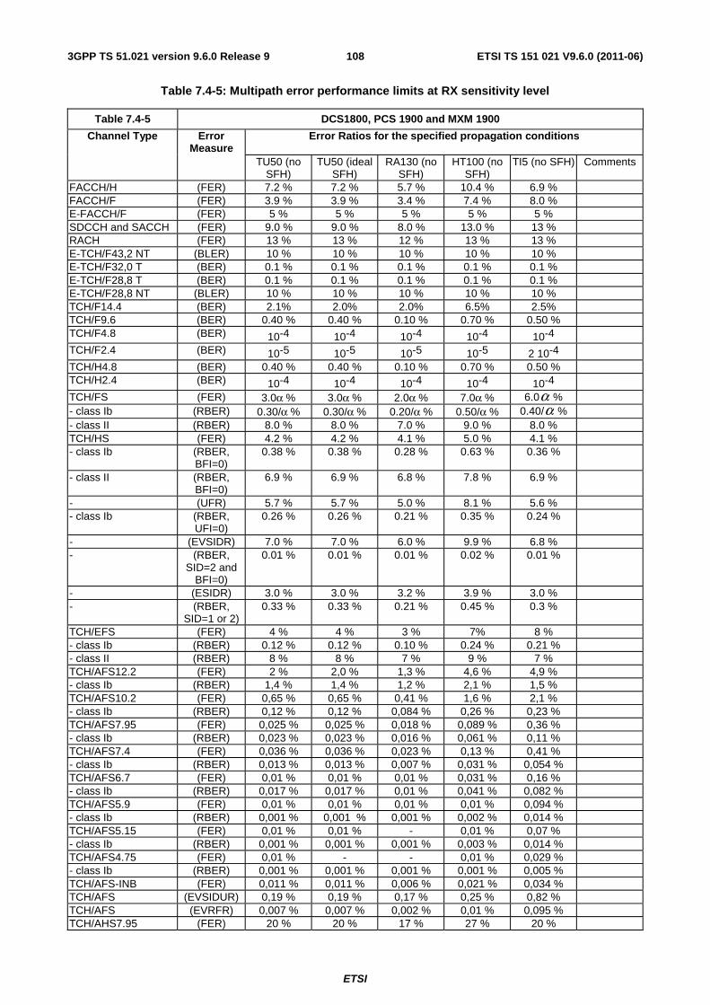
ETSI
ETSI TS 151 021 V9.6.0 (2011-06)1083GPP TS 51.021 version 9.6.0 Release 9
Table 7.4-5: Multipath error performance limits at RX sensitivity level
Table 7.4-5 DCS1800, PCS 1900 and MXM 1900
Channel Type Error Measure
Error Ratios for the specified propagation conditions
TU50 (no SFH)
TU50 (ideal SFH)
RA130 (no SFH)
HT100 (no SFH)
TI5 (no SFH) Comments
FACCH/H (FER) 7.2 % 7.2 % 5.7 % 10.4 % 6.9 % FACCH/F (FER) 3.9 % 3.9 % 3.4 % 7.4 % 8.0 % E-FACCH/F (FER) 5 % 5 % 5 % 5 % 5 % SDCCH and SACCH (FER) 9.0 % 9.0 % 8.0 % 13.0 % 13 % RACH (FER) 13 % 13 % 12 % 13 % 13 % E-TCH/F43,2 NT (BLER) 10 % 10 % 10 % 10 % 10 % E-TCH/F32,0 T (BER) 0.1 % 0.1 % 0.1 % 0.1 % 0.1 % E-TCH/F28,8 T (BER) 0.1 % 0.1 % 0.1 % 0.1 % 0.1 % E-TCH/F28,8 NT (BLER) 10 % 10 % 10 % 10 % 10 % TCH/F14.4 (BER) 2.1% 2.0% 2.0% 6.5% 2.5% TCH/F9.6 (BER) 0.40 % 0.40 % 0.10 % 0.70 % 0.50 % TCH/F4.8 (BER) 10-4 10-4 10-4 10-4 10-4
TCH/F2.4 (BER) 10-5 10-5 10-5 10-5 2 10-4
TCH/H4.8 (BER) 0.40 % 0.40 % 0.10 % 0.70 % 0.50 % TCH/H2.4 (BER) 10-4 10-4 10-4 10-4 10-4
TCH/FS (FER) 3.0α % 3.0α % 2.0α % 7.0α % 6.0α % - class Ib (RBER) 0.30/α % 0.30/α % 0.20/α % 0.50/α % 0.40/α % - class II (RBER) 8.0 % 8.0 % 7.0 % 9.0 % 8.0 % TCH/HS (FER) 4.2 % 4.2 % 4.1 % 5.0 % 4.1 % - class Ib (RBER,
BFI=0) 0.38 % 0.38 % 0.28 % 0.63 % 0.36 %
- class II (RBER, BFI=0)
6.9 % 6.9 % 6.8 % 7.8 % 6.9 %
- (UFR) 5.7 % 5.7 % 5.0 % 8.1 % 5.6 % - class Ib (RBER,
UFI=0) 0.26 % 0.26 % 0.21 % 0.35 % 0.24 %
- (EVSIDR) 7.0 % 7.0 % 6.0 % 9.9 % 6.8 % - (RBER,
SID=2 and BFI=0)
0.01 % 0.01 % 0.01 % 0.02 % 0.01 %
- (ESIDR) 3.0 % 3.0 % 3.2 % 3.9 % 3.0 % - (RBER,
SID=1 or 2) 0.33 % 0.33 % 0.21 % 0.45 % 0.3 %
TCH/EFS (FER) 4 % 4 % 3 % 7% 8 % - class Ib (RBER) 0.12 % 0.12 % 0.10 % 0.24 % 0.21 % - class II (RBER) 8 % 8 % 7 % 9 % 7 % TCH/AFS12.2 (FER) 2 % 2,0 % 1,3 % 4,6 % 4,9 % - class Ib (RBER) 1,4 % 1,4 % 1,2 % 2,1 % 1,5 % TCH/AFS10.2 (FER) 0,65 % 0,65 % 0,41 % 1,6 % 2,1 % - class Ib (RBER) 0,12 % 0,12 % 0,084 % 0,26 % 0,23 % TCH/AFS7.95 (FER) 0,025 % 0,025 % 0,018 % 0,089 % 0,36 % - class Ib (RBER) 0,023 % 0,023 % 0,016 % 0,061 % 0,11 % TCH/AFS7.4 (FER) 0,036 % 0,036 % 0,023 % 0,13 % 0,41 % - class Ib (RBER) 0,013 % 0,013 % 0,007 % 0,031 % 0,054 % TCH/AFS6.7 (FER) 0,01 % 0,01 % 0,01 % 0,031 % 0,16 % - class Ib (RBER) 0,017 % 0,017 % 0,01 % 0,041 % 0,082 % TCH/AFS5.9 (FER) 0,01 % 0,01 % 0,01 % 0,01 % 0,094 % - class Ib (RBER) 0,001 % 0,001 % 0,001 % 0,002 % 0,014 % TCH/AFS5.15 (FER) 0,01 % 0,01 % - 0,01 % 0,07 % - class Ib (RBER) 0,001 % 0,001 % 0,001 % 0,003 % 0,014 % TCH/AFS4.75 (FER) 0,01 % - - 0,01 % 0,029 % - class Ib (RBER) 0,001 % 0,001 % 0,001 % 0,001 % 0,005 % TCH/AFS-INB (FER) 0,011 % 0,011 % 0,006 % 0,021 % 0,034 % TCH/AFS (EVSIDUR) 0,19 % 0,19 % 0,17 % 0,25 % 0,82 % TCH/AFS (EVRFR) 0,007 % 0,007 % 0,002 % 0,01 % 0,095 % TCH/AHS7.95 (FER) 20 % 20 % 17 % 27 % 20 %

ETSI
ETSI TS 151 021 V9.6.0 (2011-06)1093GPP TS 51.021 version 9.6.0 Release 9
Table 7.4-5 DCS1800, PCS 1900 and MXM 1900
Channel Type Error Measure
Error Ratios for the specified propagation conditions
TU50 (no SFH)
TU50 (ideal SFH)
RA130 (no SFH)
HT100 (no SFH)
TI5 (no SFH) Comments
- class Ib (RBER) 2,3 % 2,3 % 2 % 2,9 % 2,3 % - class II (RBER) 5 % 5 % 4,8 % 5,7 % 5 % TCH/AHS7.4 (FER) 16 % 16 % 13 % 22 % 16 % - class Ib (RBER) 1,4 % 1,4 % 1,1 % 1,9 % 1,4 % - class II (RBER) 5,3 % 5,3 % 5,1 % 6,1 % 5,3 % TCH/AHS6.7 (FER) 9,4 % 9,4 % 7,5 % 13 % 9,2 % - class Ib (RBER) 1,1 % 1,1 % 0,92 % 1,5 % 1,1 % - class II (RBER) 5,8 % 5,8 % 5,5 % 6,6 % 5,8 % TCH/AHS5.9 (FER) 5,9 % 5,9 % 4,6 % 8,5 % 5,7 % - class Ib (RBER) 0,52 % 0,52 % 0,39 % 0,72 % 0,51 % - class II (RBER) 6,1 % 6,1 % 5,8 % 6,8 % 6 % TCH/AHS5.15 (FER) 2,6 % 2,6 % 2 % 3,7 % 2,5 % - class Ib (RBER) 0,53 % 0,53 % 0,4 % 0,76 % 0,51 % - class II (RBER) 6,3 % 6,3 % 6,1 % 7,2 % 6,3 % TCH/AHS4.75 (FER) 1,2 % 1,2 % 1,1 % 1,7 % 1,2 % - class Ib (RBER) 0,18 % 0,18 % 0,13 % 0,25 % 0,17 % - class II (RBER) 6,5 % 6,5 % 6,2 % 7,3 % 6,4 % TCH/AHS-INB (FER) 0,64 % 0,64 % 0,53 % 0,94 % 0,72 % TCH/AHS (EVSIDUR) 1,3 % 1,3 % 2,1 % 1,5 % 1,5 % TCH/AHS (EVRFR) 0,24 % 0,24 % 0,25 % 0,24 % 0,25 % PDTCH/CS-1 to 4 (BLER) 10% 10% 10% 10% 10 % PDTCH/MCS-1 to 6 (BLER) 10% 10% 10% 10% 10% PDTCH/MCS-7 (BLER) 10 % 10 % 30 % - 10 % PDTCH/MCS-8 (BLER) 30 % 30 % - - 30 % PDTCH/MCS-9 (BLER) 30 % 30 % - - 30 % PDTCH/UAS-7 (BLER) 10 % 10 % 10 % 10 % 10 % PDTCH/UAS-8 to 9 (BLER) 10% 10% 10% 30% 10% PDTCH/UAS-10 (BLER) 10% 10% 30% - 10% PDTCH/UAS-11 (BLER) 30% 30% - - 30% PDTCH/UBS-5 to 12 (BLER) 10% 2) 10% 10% 2) 10% 2) 10% 2) PDTCH/UBS-8 (BLER) 10% 2) 10% 10% 2) 10% 3) 10% 2) PDTCH/UBS-9 (BLER) 10% 2) 10% 10% 2) 10% 3) 10% 2) PDTCH/UBS-10 (BLER) 10% 2) 10% 10% 2) 30% 2) 10% 2) PDTCH/UBS-11 (BLER) 10% 2) 10% 30% 2) - 10% 2) PDTCH/UBS-12 (BLER) 10% 2) 10% 30% 2) - 10% 2) PRACH/11 bit (BLER) 15% 15% 15% 15% 15 % PRACH/8 bit (BLER) 15% 15% 15% 15% 15 % PACCH (BLER) 10% 10% 10% 10% 10 % TCH/WFS12.65 (FER) 1% 1% 1% 1% 1% (RBER) 0,62 % 0,62 % 0,72 % 0,66 % 0,35 % TCH/ WFS8.85 (FER) 1% 1% 1% 1% 1% (RBER) 0,59 % 0,59 % 0,72 % 0,58 % 0,38 % TCH/ WFS6.60 (FER) 1% 1% 1% 1% 1% (RBER) 0,17 % 0,17 % 0,19 % 0,25 % 0,15 % O-FACCH/F (FER) 5 % 5 % 5 % 5 % 5 %
O-FACCH/H (FER) 5 % 5 % 5 % 5 % 5 % O-TCH/AHS12.2 (FER) 1 % 1 % 1 % 1 % 1 % - class Ib (RBER) 0,30 % 0,30 % 1 % 0,42 % 0,30 % O-TCH/AHS10.2 (FER) 1 % 1 % 0,29 % 1 % 1 % - class Ib (RBER) 0,17 % 0,17 % 1 % 0,20 % 0,15 % O-TCH/AHS7.95 (FER) 1 % 1 % 0,13 % 1 % 1 % - class Ib (RBER) 0,08 % 0,08 % 1 % 0,08 % 0,08 % O-TCH/AHS7.4 (FER) 1 % 1 % 0,05 % 1 % 1 % - class Ib (RBER) 0,15 % 0,15 % 1 % 0,17 % 0,15 % O-TCH/AHS6.7 (FER) 1 % 1 % 0,12 % 1 % 1 % - class Ib (RBER) 0,16 % 0,16 % 1 % 0,19 % 0,14 % O-TCH/AHS5.9 (FER) 1 % 1 % 0,12 % 1 % 1 % - class Ib (RBER) 0,22 % 0,22 % 1 % 0,24 % 0,20 %

ETSI
ETSI TS 151 021 V9.6.0 (2011-06)1103GPP TS 51.021 version 9.6.0 Release 9
Table 7.4-5 DCS1800, PCS 1900 and MXM 1900
Channel Type Error Measure
Error Ratios for the specified propagation conditions
TU50 (no SFH)
TU50 (ideal SFH)
RA130 (no SFH)
HT100 (no SFH)
TI5 (no SFH) Comments
O-TCH/AHS5.15 (FER) 1 % 1 % 0,15 % 1 % 1 % - class Ib (RBER) 0,11 % 0,11 % 1 % 0,12 % 0,10 % O-TCH/AHS4.75 (FER) 1 % 1 % 0,07 % 1 % 1 % - class Ib (RBER) 0,15 % 0,15 % 1 % 0,17 % 0,15 % O-TCH/AHS-INB (FER) 0.5 % 0.5 % 0.5 % 0.5 % 0.5 % O-TCH/AHS (EVSIDUR) 1 % 1 % 1 % 1 % 1 %
O-TCH/AHS (EVRFR) 1 % 1 % 1 % 1 % 1 % O-TCH/WFS23.85 (FER) 1 % 1 % 1 % 1 % 1 % - class Ib (RBER) 0,17 % 0,17 % 0,24 % 0,26 % 0,16 % O-TCH/WFS15.85 (FER) 1 % 1 % 1 % 1 % 1 % - class Ib (RBER) 0,50 % 0,50 % 0,64 % 0,60 % 0,44 % O-TCH/WFS12.65 (FER) 1 % 1 % 1 % 1 % 1 % - class Ib (RBER) 0,45 % 0,45 % 0,51 % 0,63 % 0,37 % O-TCH/WFS8.85 (FER) 1 % 1 % 1 % 1 % 1 % - class Ib (RBER) 0,38 % 0,38 % 0,42 % 0,57 % 0,31 % O-TCH/WFS6.60 (FER) 1 % 1 % 1 % 1 % 1 % - class Ib (RBER) 0,20 % 0,20 % 0,23 % 0,30 % 0,18 % O-TCH/WFS-INB (FER) 0.5 % 0.5 % 0.5 % 0.5 % 0.5 % O-TCH/WFS (EVSIDUR) 1 % 1 % 1 % 1 % 1 % O-TCH/WFS (EVRFR) 1 % 1 % 1 % 1 % 1 % O-TCH/WHS12.65 (FER) 1 % 1 % 1 % 1 % 1 % - class Ib (RBER) 0,34 % 0,34 % 0,30 % 0,44 % 0,30 % O-TCH/WHS8.85 (FER) 1 % 1 % 1 % 1 % 1 % - class Ib (RBER) 0,12 % 0,12 % 0,10 % 0,15 % 0,10 % O-TCH/WHS6.60 (FER) 1 % 1 % 1 % 1 % 1 % - class Ib (RBER) 0,16 % 0,16 % 0,13 % 0,19 % 0,15 % O-TCH/WHS-INB (FER) 0.5 % 0.5 % 0.5 % 0.5 % 0.5 % O-TCH/WHS (EVSIDUR) 1 % 1 % 1 % 1 % 1 % O-TCH/WHS (EVRFR) 1 % 1 % 1 % 1 % 1 % TCH/HS (FER) [1 %] - - - - VAMOS
mode with 0 dB SCPIR
- class Ib (RBER) [tbd] - - - - - class II (RBER) [tbd] - - - - TCH/EFS (FER) [1 %] - - - - - class Ib (RBER) [tbd] - - - - - class II (RBER) [tbd] - - - - TCH/AFS 12.2 (FER) [1 %] - - - - - class Ib (RBER) [tbd] - - - - TCH/AFS 4.75 (FER) [1 %] - - - - - class Ib (RBER) [tbd] - - - - TCH/AHS 7.4 (FER) [1 %] - - - - - class Ib (RBER) [tbd] - - - - - class II (RBER) [tbd] - - - - TCH/AHS 4.75 (FER) [1 %] - - - - - class Ib (RBER) [tbd] - - - - - class II (RBER) [tbd] - - - - TCH/WFS 12.65 (FER) [1 %] - - - - - class Ib (RBER) [tbd] - - - - TCH/WFS 6.60 (FER) [1 %] - - - - - class Ib (RBER) [tbd] - - - - FACCH/F (FER) [5 %] - - - - FACCH/H (FER) [5 %] - - - - SACCH (FER) [5 %] - - - - Repeated SACCH (FER) [5 %] - - - - TCH/HS (FER) [1 %] - - - - VAMOS
mode with -10 dB SCPIR
- class Ib (RBER) [tbd] - - - - - class II (RBER) [tbd] - - - - TCH/EFS (FER) [1 %] - - - - - class Ib (RBER) [tbd] - - - -

ETSI
ETSI TS 151 021 V9.6.0 (2011-06)1113GPP TS 51.021 version 9.6.0 Release 9
Table 7.4-5 DCS1800, PCS 1900 and MXM 1900
Channel Type Error Measure
Error Ratios for the specified propagation conditions
TU50 (no SFH)
TU50 (ideal SFH)
RA130 (no SFH)
HT100 (no SFH)
TI5 (no SFH) Comments
- class II (RBER) [tbd] - - - - TCH/AFS 12.2 (FER) [1 %] - - - - - class Ib (RBER) [tbd] - - - - TCH/AHS 7.4 (FER) [1 %] - - - - - class Ib (RBER) [tbd] - - - - - class II (RBER) [tbd] - - - - TCH/WFS 12.65 (FER) [1 %] - - - - - class Ib (RBER) [tbd] - - - - NOTE 1: The performance requirements for TCH/WFS inband signalling, SID_UPDATE and RATSCCH are the same
as those given for TCH/AFS. It is sufficient to test inband signalling, SID_UPDATE and RATSCCH requirements for only one of the channel types TCH/AFS and TCH/WFS.
NOTE 2: No requirement apply for wanted signal narrow. NOTE 3: 30% BLER requirement apply for wanted signal narrow. The value of α in tables 7.4-4 and 7.4-5 shall be between 1 and 1.6, and shall be the same for both occurrences in each propagation condition; it may be different for different propagation conditions.
NOTE: For each TU50 (ideal FH), sufficient decorrelation may be achieved with 4 frequencies spaced over 5 MHz.
7.4.5 Requirement Reference
3GPP TS 45.005 subclause 6.2.
7.5 Reference interference level
7.5.1 Test Purpose
The reference interference level is a measure of the capability of the receiver to receive a wanted modulated signal without exceeding a given degradation due to the presence of an unwanted modulated signal at the same carrier frequency (co-channel interference) or at any adjacent carrier frequencies (adjacent channel interference).
7.5.2 Test Case
If Slow Frequency Hopping (SFH) is supported by the BSS, it shall be disabled during this measurement, except when performing tests using propagation conditions with ideal SFH.
When SFH is used in the test, the BSS shall hop over the maximum range and number of ARFCNs possible for the test environment and which are available in the BSS configuration. If SFH is not supported, the test shall be performed on the specified number of ARFCNs. As a minimum, one time slot shall be tested on one TRX.
The tests shall be performed in a single-antenna configuration except in case of packet-switched channels with higher symbol rate and channels in VAMOS mode where two-antenna configuration with no correlation or gain difference between the branches is used.
Two input signals shall be connected to the respective receiver connector via a combining network. When testing each signal shall be connected through a Multipath Fading Simulator (MFS) as described in annex B.1, except in the cases of frequency offsets of the interfering signal from the wanted signal of 400kHz or greater, where the interferer shall be static, unless otherwise stated in table 7.5-2 and 7.5-3. The multipath fading propagation conditions shall be uncorrelated. In the case of channels in VAMOS mode, two input wanted signals and two input interfering signals shall be connected to each receiver antenna connector via a Multipath Fading Simulator such that the multipath fading propagation conditions between all the input signals and all the receiver antennas are uncorrelated. The frequency offsets and the relative levels of the interfering signals are defined in table 7.5-1a for test scenarios VUTS-1, VUTS-2, VUTS-3 and VUTS-4. The wanted signals VAMOS sub-channel 1 and VAMOS sub-channel 2 shall be GMSK modulated and encoded according to the channel type in table 7.5-5a. The interfering signals shall be GMSK
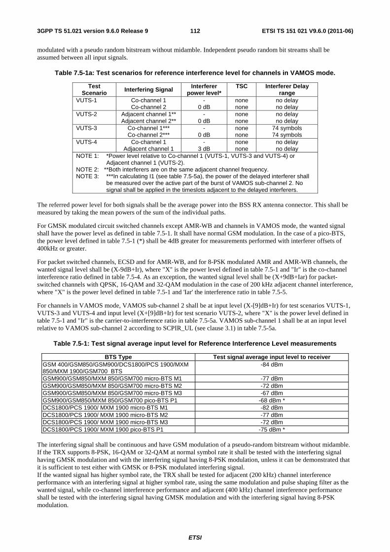
ETSI
ETSI TS 151 021 V9.6.0 (2011-06)1123GPP TS 51.021 version 9.6.0 Release 9
modulated with a pseudo random bitstream without midamble. Independent pseudo random bit streams shall be assumed between all input signals.
Table 7.5-1a: Test scenarios for reference interference level for channels in VAMOS mode.
Test Scenario Interfering Signal Interferer
power level* TSC Interferer Delay
range VUTS-1 Co-channel 1
Co-channel 2 -
0 dB none none
no delay no delay
VUTS-2 Adjacent channel 1** Adjacent channel 2**
- 0 dB
none none
no delay no delay
VUTS-3 Co-channel 1*** Co-channel 2***
- 0 dB
none none
74 symbols 74 symbols
VUTS-4 Co-channel 1 Adjacent channel 1
- 3 dB
none none
no delay no delay
NOTE 1: *Power level relative to Co-channel 1 (VUTS-1, VUTS-3 and VUTS-4) or Adjacent channel 1 (VUTS-2).
NOTE 2: **Both interferers are on the same adjacent channel frequency. NOTE 3: ***In calculating I1 (see table 7.5-5a), the power of the delayed interferer shall
be measured over the active part of the burst of VAMOS sub-channel 2. No signal shall be applied in the timeslots adjacent to the delayed interferers.
The referred power level for both signals shall be the average power into the BSS RX antenna connector. This shall be measured by taking the mean powers of the sum of the individual paths.
For GMSK modulated circuit switched channels except AMR-WB and channels in VAMOS mode, the wanted signal shall have the power level as defined in table 7.5-1. It shall have normal GSM modulation. In the case of a pico-BTS, the power level defined in table 7.5-1 (*) shall be 4dB greater for measurements performed with interferer offsets of 400kHz or greater.
For packet switched channels, ECSD and for AMR-WB, and for 8-PSK modulated AMR and AMR-WB channels, the wanted signal level shall be (X-9dB+Ir), where "X" is the power level defined in table 7.5-1 and "Ir" is the co-channel interference ratio defined in table 7.5-4. As an exception, the wanted signal level shall be (X+9dB+Iar) for packet-switched channels with QPSK, 16-QAM and 32-QAM modulation in the case of 200 kHz adjacent channel interference, where "X" is the power level defined in table 7.5-1 and 'Iar' the interference ratio in table 7.5-5.
For channels in VAMOS mode, VAMOS sub-channel 2 shall be at input level (X-[9]dB+Ir) for test scenarios VUTS-1, VUTS-3 and VUTS-4 and input level (X+[9]dB+Ir) for test scenario VUTS-2, where "X" is the power level defined in table 7.5-1 and "Ir" is the carrier-to-interference ratio in table 7.5-5a. VAMOS sub-channel 1 shall be at an input level relative to VAMOS sub-channel 2 according to SCPIR_UL (see clause 3.1) in table 7.5-5a.
Table 7.5-1: Test signal average input level for Reference Interference Level measurements
BTS Type Test signal average input level to receiver GSM 400/GSM850/GSM900/DCS1800/PCS 1900/MXM 850/MXM 1900/GSM700 BTS
-84 dBm
GSM900/GSM850/MXM 850/GSM700 micro-BTS M1 -77 dBm GSM900/GSM850/MXM 850/GSM700 micro-BTS M2 -72 dBm GSM900/GSM850/MXM 850/GSM700 micro-BTS M3 -67 dBm GSM900/GSM850/MXM 850/GSM700 pico-BTS P1 -68 dBm * DCS1800/PCS 1900/ MXM 1900 micro-BTS M1 -82 dBm DCS1800/PCS 1900/ MXM 1900 micro-BTS M2 -77 dBm DCS1800/PCS 1900/ MXM 1900 micro-BTS M3 -72 dBm DCS1800/PCS 1900/ MXM 1900 pico-BTS P1 -75 dBm *
The interfering signal shall be continuous and have GSM modulation of a pseudo-random bitstream without midamble. If the TRX supports 8-PSK, 16-QAM or 32-QAM at normal symbol rate it shall be tested with the interfering signal having GMSK modulation and with the interfering signal having 8-PSK modulation, unless it can be demonstrated that it is sufficient to test either with GMSK or 8-PSK modulated interfering signal. If the wanted signal has higher symbol rate, the TRX shall be tested for adjacent (200 kHz) channel interference performance with an interfering signal at higher symbol rate, using the same modulation and pulse shaping filter as the wanted signal, while co-channel interference performance and adjacent (400 kHz) channel interference performance shall be tested with the interfering signal having GMSK modulation and with the interfering signal having 8-PSK modulation.

ETSI
ETSI TS 151 021 V9.6.0 (2011-06)1133GPP TS 51.021 version 9.6.0 Release 9
If the TRX does not support 8-PSK it shall be tested with the interfering signal having GMSK modulation. For SFH this interferer shall consist of either one signal which hops in synchronization with the time slot under test or a number of fixed frequency signal sources. In the latter case the number of interfering sources determines the number of frequencies over which the time slot under test can hop in the test environment irrespective of the upper limit of the BTS.
For packet-switched channels only BTTI without PAN need to be tested.
When testing 16-QAM, 32-QAM (both normal and higher symbol rate) and QPSK modulated channels TSC-6 shall be used for the wanted signal.
For GMSK modulated circuit switched channels except AMR-WB and channels in VAMOS mode, the test shall be performed with frequency offsets of the interfering signal from the wanted signal, for a relative level of interfering signal above the wanted signal as specified in table 7.5-2. In some cases a second requirement is specified, where the interference ratio in table 7.5-2 shall be increased or decreased by 3 dB. In these cases the Error measures are noted as FER@+3dB or FER@-3dB respectively.
For packet switched channels, ECSD and AMR-WB, and 8-PSK modulated AMR and AMR-WB channels except channels in VAMOS mode, the test shall be performed with frequency offsets of the interfering signal from the wanted signal, for a carrier to interferer ratio, relative to the co-channel interference ratio (C/Ic), as specified in table 7.5-3. The minimum co-channel interference ratio (C/Ic) for all the combinations of logical channel type and propagation condition are as specified in table 7.5-4.
For channels in VAMOS mode, the test shall be performed for the test scenarios in table 7.5-1 with a carrier to interferer ratio in table 7.5-5a. The minimum carrier to interference ratios are as specified in table 7.5-5a.
In the case of Slow Frequency Hopping (SFH) the interfering signal shall be on the same ARFCN as the wanted signal over the useful part of the time slot burst. For offsets greater than 0 kHz only the multipath propagation condition TU50 (no SFH) need be tested for normal and micro-BTS systems, and only the multipath propagation condition TI5 (no SFH) need be tested for pico-BTS systems.
Table 7.5-2: Co-channel and adjacent channel interference rejections for circuit switched channels except ECSD and AMR-WB channels, and 8-PSK modulated AMR and AMR-WB channels
Interferers offset: Carrier to Interferer Ratio: Fading of interferer Normal and Micro-BTS Pico-BTS
0 kHz 9 dB 13 dB yes 200 kHz -9 dB -5 dB yes 400 kHz -41 dB -37dB no
Table 7.5-3: Co-channel and adjacent channel interference ratios for packet switched channels, for ECSD and for AMR-WB channels, and for 8-PSK modulated AMR and AMR-WB channels
Modulation of wanted signal
GMSK 8-PSK 16-QAM and 32-QAM with normal
symbol rate
QPSK, 16-QAM and 32-QAM with
higher symbol rate
Interferers offset: Carrier to Interferer Ratio
Carrier to Interferer Ratio
Carrier to Interferer Ratio
Carrier to Interferer Ratio
Fading of interferer
0 kHz C/Ic (table 7.5-4) C/Ic (table 7.5-4) C/Ic (table 7.5-4) C/Ic (table 7.5-4) yes 200 kHz C/Ic - 18 dB Table 7.5-5 Table 7.5-5 Table 7.5-5 yes 400 kHz C/Ic - 50 dB C/Ic - 50 dB C/Ic – 48 dB C/Ic – 44.5 dB
(QPSK) C/Ic – 43 dB
(16QAM) C/Ic – 42.5 dB
(32QAM)
yes
For QPSK, 16-QAM and 32-QAM modulated channels with higher symbol rate, the wanted signal shall be generated with wide pulse shaping filter when testing for co-channel and adjacent (400 kHz) channel performance. For tests of adjacent (200 kHz) channel performance the input signals shall be generated with pulse shaping filters according to table 7.5-5.
For channels in VAMOS mode, a time and frequency offset shall be applied to VAMOS sub-channel 1 relative to VAMOS sub-channel 2. The offsets shall be applied burst-wise and taken from a sample sequence that conforms to the

ETSI
ETSI TS 151 021 V9.6.0 (2011-06)1143GPP TS 51.021 version 9.6.0 Release 9
probability distribution in Eq 7.5.2a for the time offset and Eq 7.5.2b for the frequency offset, where σ and μ are
given in the table below:
Frequency Band 850/900 1800 1900 μ 45 Hz 90 Hz 95 Hz σ 10 Hz 17 Hz 17 Hz
⎪⎪
⎩
⎪⎪
⎨
⎧
==
−==
else
PeriodsSymbolNormaloffsetTimeforPeriodsSymbolNormaloffsetTimefor
PeriodsSymbolNormaloffsetTimefor
offsetTimep
,0
1,25.00,5.0
1,25.0
)( (Eq 7.5.2a)
( )
2
2
22
1)(
σπσ
μ−−=
offsetFrequency
eoffsetFrequencyp (Eq 7.5.2b)
NOTE: The precise sample sequence for each offset has been left for test equipment manufacturers to specify.

ETSI
ETSI TS 151 021 V9.6.0 (2011-06)1153GPP TS 51.021 version 9.6.0 Release 9
Table 7.5-4: Co-channel interference ratios (C/Ic) for packet switched channels, for ECSD and for AMR-WB channels, and for 8-PSK modulated AMR and AMR-WB channels
Table 7.5-4 GSM 400, GSM 700, GSM900, GSM 850 and MXM 850***
Channel Type Unit Carrier to Interferer Ratios for specified propagation conditions TU3
(no SFH) TU50
(no SFH) TU50
(ideal SFH) RA250
(no SFH) TI5
(no SFH) PDTCH/CS-1 dB 13 10 9 9 14
PDTCH/CS-2 dB 15 14 13 13 18
PDTCH/CS-3 dB 16 16 15 16 20
PDTCH/CS-4 dB 21 24 24 * 27
PDTCH/MCS-1 dB 13 10.5 9.5 10 14.5
PDTCH/MCS-2 dB 15 12.5 12 12 16.5
PDTCH/MCS-3 dB 16.5 17 17 19 21
PDTCH/MCS-4 dB 19 22 22 * 26
PDTCH/MCS-5 dB 18 15.5 14.5 16 19.5
PDTCH/MCS-6 dB 20 18 17.5 21 22
PDTCH/MCS-7 dB 23.5 24 24.5 26.5** 28
PDTCH/MCS-8 dB 28.5 30 30 * 34
PDTCH/MCS-9 dB 30 33 35 * 37
PDTCH/UAS-7 dB 27 23.5 22.5 22 27.5
PDTCH/UAS-8 dB 28 25 24.5 25.5 29
PDTCH/UAS-9 dB 28.5 27 26.5 33 31
PDTCH/UAS-10 dB 29.5 29.5 29.5 34.5** 33.5
PDTCH/UAS-11 dB 30.5 33 33 * 37
PDTCH/UBS-5 dB -4.5 -4.5 -6.0 -1.5 -0.5
PDTCH/UBS-6 dB -2.0 -3.0 -3.5 1.5 1.0
PDTCH/UBS-7 dB 2.5 1.5 1.0 5.5 5.5
PDTCH/UBS-8 dB 4.5 4.0 3.5 9.5 8.0
PDTCH/UBS-9 dB 5.5 5.5 5.0 13.0 9.5
PDTCH/UBS-10 dB 11.0 12.5 12.0 26.0 16.5
PDTCH/UBS-11 dB 13.5 16.5 17.0 35.0 20.5
PDTCH/UBS-12 dB 15.0 19.5 19.5 28.0** 23.5
E-TCH/F43,2 NT dB 24 19.5 19 21.5 23.5
E-TCH/F32,0 T dB 25.5 17 15.5 15.5 21
E-TCH/F28,8 T dB 27 17.5 15.5 16 21.5
E-TCH/F28,8 NT dB 20 14.5 13.5 13.5 18.5
E-FACCH/F dB 17.5 12.5 11.5 11.5 16.5
PACCH dB 13 10 9 9 14
PRACH/11 bits dB 8 8 8 10 12
PRACH/8 bits dB 8 8 8 9 12
TCH/WFS12.65 dB 21,5 14,5 13 12,5 18,5
TCH/ WFS8.85 dB 20 11,5 10 9 15,5
TCH/ WFS6.60 dB 19 10,5 9 8 14,5
O-FACCH/F dB 15,5 10 8 9 14
O-FACCH/H dB 15,5 10 9 9,5 14
O-TCH/AHS12.2 dB 22,5 16,5 15,5 17 20,5
O-TCH/AHS10.2 dB 21,5 15,5 14,5 15,5 19,5
O-TCH/AHS7.95 dB 20,5 14,5 13,5 14,5 18,5
O-TCH/AHS7.4 dB 20 14 12,5 13,5 18
O-TCH/AHS6.7 dB 19,5 13,5 12 13 17,5
O-TCH/AHS5.9 dB 19 13 12 12,5 17
O-TCH/AHS5.15 dB 18,5 12,5 11 12 16,5
O-TCH/AHS4.75 dB 18 12 10,5 11,5 16

ETSI
ETSI TS 151 021 V9.6.0 (2011-06)1163GPP TS 51.021 version 9.6.0 Release 9
Table 7.5-4 GSM 400, GSM 700, GSM900, GSM 850 and MXM 850***
O-TCH/AHS-INB (FER)
dB 16,5 10,5 10,5 12,5 14,5
O-TCH/AHS (EVSIDUR)
dB 16 10,5 9,5 10,5 14,5
O-TCH/AHS (EVRFR)
dB 16 10,5 9,5 11 14,5
O-TCH/WFS23.85 dB 22,5 16 13,5 13,5 20
O-TCH/WFS15.85 dB 20 13,5 11 10,5 17,5
O-TCH/WFS12.65 dB 18,5 11,5 9,5 9,5 15,5
O-TCH/WFS8.85 dB 17 10,5 7,5 7,5 14,5
O-TCH/WFS6.60 dB 16 9,5 7 6,5 13,5
O-TCH/WFS-INB (FER)
dB 14,5 7 6 6 11
O-TCH/WFS (EVSIDUR)
dB 17,5 11,5 9,5 9,5 15,5
O-TCH/WFS (EVRFR)
dB 16,5 10 7,5 7,5 14
O-TCH/WHS12.65 dB 22,5 17 15,5 17 21
O-TCH/WHS8.85 dB 21 15 14 15 19
O-TCH/WHS6.60 dB 19,5 13,5 12 13 17,5
O-TCH/WHS-INB (FER)
dB 16,5 10,5 10,5 12,5 14,5
O-TCH/WHS (EVSIDUR)
dB 16 10,5 9,5 10,5 14,5
O-TCH/WHS (EVRFR)
dB 16 10,5 9,5 11 14,5

ETSI
ETSI TS 151 021 V9.6.0 (2011-06)1173GPP TS 51.021 version 9.6.0 Release 9
Table 7.5-4 DCS1800, PCS 1900 and MXM1900***
Channel Type Unit Carrier to Interferer Ratios for specified propagation conditions
TU1.5 (no SFH)
TU50 (no SFH)
TU50 (ideal SFH)
RA130 (no SFH)
TI5 (no SFH)
PDTCH/CS-1 dB 13 9 9 9 14
PDTCH/CS-2 dB 15 13 13 13 18
PDTCH/CS-3 dB 16 16 16 16 20
PDTCH/CS-4 dB 21 27 27 * 27
PDTCH/MCS-1 dB 13 10 9.5 10 14.5
PDTCH/MCS-2 dB 15 12 12 12 16.5
PDTCH/MCS-3 dB 16.5 17 18 19 21
PDTCH/MCS-4 dB 19 23 23 * 26
PDTCH/MCS-5 dB 18 15 15 16 19.5
PDTCH/MCS-6 dB 20 17.5 18 21 22
PDTCH/MCS-7 dB 23.5 26 26.5 27** 28
PDTCH/MCS-8 dB 28.5 25** 24.5** * 34
PDTCH/MCS-9 dB 30 29** 29** * 37
PDTCH/UAS-7 dB 27 23 23 22 27.5
PDTCH/UAS-8 dB 28 25 25 25.5 29
PDTCH/UAS-9 dB 28.5 26 26 33 31
PDTCH/UAS-10 dB 29.5 26.5** 26.5** 34.5** 33.5
PDTCH/UAS-11 dB 30.5 29.5** 29.5** * 37
PDTCH/UBS-5 dB -4.5 -4.5 -4.5 -1.5 -0.5
PDTCH/UBS-6 dB -2.0 -2.5 -2.5 1.5 1.0
PDTCH/UBS-7 dB 2.5 2.5 2.5 5.5 5.5
PDTCH/UBS-8 dB 4.5 5.0 5.0 9.5 8.0
PDTCH/UBS-9 dB 5.5 6.5 6.5 13.0 9.5
PDTCH/UBS-10 dB 11.0 14.5 14.5 26.0 16.5
PDTCH/UBS-11 dB 13.5 22.5 22.5 35.0 20.5
PDTCH/UBS-12 dB 15.0 28.5 28.5 28.0** 23.5
E-TCH/F43,2 NT dB 24 19.5 19.5 22 23.5
E-TCH/F32,0 T dB 25.5 16 15.5 15.5 21
E-TCH/F28,8 T dB 27 16 16 17 21.5
E-TCH/F28,8 NT dB 20 14 14 14.5 18.5
E-FACCH/F dB 17.5 11.5 11.5 11.5 16.5
PACCH dB 13 9 9 9 14
PRACH/11 bits dB 9 9 9 10 12
PRACH/8 bits dB 8 8 8 9 12
TCH/WFS12.65 dB 21,5 13 13 12,5 18,5
TCH/ WFS8.85 dB 20 10 10 9 15,5
TCH/ WFS6.60 dB 19 9 9 8 14,5
O-FACCH/F dB 15,5 9 9 9 14
O-FACCH/H dB 15,5 9,5 9,5 9,5 14
O-TCH/AHS12.2 dB 22,5 16,5 16,5 17 20,5
O-TCH/AHS10.2 dB 21,5 15,5 15,5 15,5 19,5
O-TCH/AHS7.95 dB 20,5 14,5 14,5 14,5 18,5
O-TCH/AHS7.4 dB 20 14 14 13,5 18
O-TCH/AHS6.7 dB 19,5 13 13 13 17,5
O-TCH/AHS5.9 dB 19 12,5 12,5 12,5 17
O-TCH/AHS5.15 dB 18,5 12 12 12 16,5
O-TCH/AHS4.75 dB 18 11,5 11,5 11,5 16
O-TCH/AHS-INB (FER)
dB 16,5 11 11 12,5 14,5

ETSI
ETSI TS 151 021 V9.6.0 (2011-06)1183GPP TS 51.021 version 9.6.0 Release 9
Table 7.5-4 DCS1800, PCS 1900 and MXM1900***
O-TCH/AHS (EVSIDUR)
dB 16 10,5 10,5 10,5 14,5
O-TCH/AHS (EVRFR)
dB 16 10,5 10,5 11 14,5
O-TCH/WFS23.85 dB 22,5 14,5 14,5 13,5 20
O-TCH/WFS15.85 dB 20 12 12 10,5 17,5
O-TCH/WFS12.65 dB 18,5 10,5 10,5 9,5 15,5
O-TCH/WFS8.85 dB 17 9 9 7,5 14,5
O-TCH/WFS6.60 dB 16 8 8 6,5 13,5
O-TCH/WFS-INB (FER)
dB 14,5 6,5 6,5 6 11
O-TCH/WFS (EVSIDUR)
dB 17,5 11 11 9,5 15,5
O-TCH/WFS (EVRFR)
dB 16,5 9 9 7,5 14
O-TCH/WHS12.65 dB 22,5 16,5 16,5 17 21
O-TCH/WHS8.85 dB 21 14,5 14,5 15 19
O-TCH/WHS6.60 dB 19,5 13 13 13 17,5
O-TCH/WHS-INB (FER)
dB 16,5 11 11 12,5 14,5
O-TCH/WHS (EVSIDUR)
dB 16 10,5 10,5 10,5 14,5
O-TCH/WHS (EVRFR)
dB 16 10,5 10,5 11 14,5
NOTE 1: PDTCH/CS-4, MCS-x and UAS-x shall not be tested for the propagation conditions marked as (*). NOTE 2: For GSM 400 the speeds shall be doubled (e.g. TU50 shall be TU100) and for GSM 700 the speeds shall
be multiplied by 1,2 (e.g. TU50 shall be TU60). NOTE 3: Performance is specified at 30% BLER for those cases marked as (**). ***NOTE 4: PDTCH/CS-1 to 4 and ECSD are not applicable for MXM850 and MXM1900. NOTE 5: PDTCH/UBS-5 to 12 requirements assume two-antenna configuration. The wanted signal shall use
higher symbol rate and be generated with wide pulse shaping filter. The interfering signal shall use GMSK and 8-PSK modulation.

ETSI
ETSI TS 151 021 V9.6.0 (2011-06)1193GPP TS 51.021 version 9.6.0 Release 9
Table 7.5-5 adjacent channel interference ratios (C/Ia) for EGPRS, EGPRS2, ECSD and 8-PSK modulated AMR and AMR-WB channels
Table 7.5-5 GSM 400, GSM 700, GSM900, GSM850 and MXM 850***
Channel Type Unit Carrier to Interferer Ratios for specified propagation conditions TU3
(no SFH) TU50
(no SFH) TU50
(ideal SFH) RA250
(no SFH) TI5
(no SFH) Comment
PDTCH/MCS-5 dB 2.5 -2 -2 1 2
PDTCH/MCS-6 dB 4.5 1 1 6.5 5
PDTCH/MCS-7 dB 8 8.5 8.5 13.5** 12.5
PDTCH/MCS-8 dB 10.5 9** 9.5** * 13**
PDTCH/MCS-9 dB 12 13.5** 13.5** * 17.5**
PDTCH/UAS-7 dB 13 9.5 8 10.5 13.5
PDTCH/UAS-8 dB 14.5 11 10 15 15
PDTCH/UAS-9 dB 15.5 13.5 12.5 22.5 17.5
PDTCH/UAS-10 dB 17.5 17 17 25** 21
PDTCH/UAS-11 dB 19 23.5 24 - 27.5
PDTCH/UBS-5 dB -17.5 -16.5 -17.0 -9.0 -12.5 Input signals generated with wide
pulse-shaping filter
(Note 5)
PDTCH/UBS-6 dB -15.0 -14.0 -14.5 -5.5 -10.0
PDTCH/UBS-7 dB -11.5 -9.5 -9.5 -2.5 -5.5
PDTCH/UBS-8 dB -8.0 -6.0 -6.0 1.5 -2.0
PDTCH/UBS-9 dB -6.0 -3.5 -4.0 4.0 0.5
PDTCH/UBS-10 dB 0.0 1.0 1.0 12.5 5.0
PDTCH/UBS-11 dB 5.5 9.0 9.0 25.0 13.0
PDTCH/UBS-12 dB 8.0 13.5 12.5 16.5** 17.5
PDTCH/UBS-5 dB -14.5 -14.0 -14.0 -2.5 -10.0 Input signals generated
with narrow pulse-shaping
filter (Note 5)
PDTCH/UBS-6 dB -12.0 -11.0 -11.5 1.5 -7.0
PDTCH/UBS-7 dB -1.5 -2.5 -3.0 7.0 1.5
PDTCH/UBS-8 dB 1.0 0.5 0.5 11.0 4.5
PDTCH/UBS-9 dB 2.5 2.0 2.0 12.5 6.0
PDTCH/UBS-10 dB 7.0 9.0 9.0 18.0 13.0
PDTCH/UBS-11 dB 8.5 13.0 13.5 18.5** 17.0
PDTCH/UBS-12 dB 9.0 14.5 15.0 22.5** 18.5
E-TCH/F43,2 NT dB 8 3.5 2.5 12 7.5
E-TCH/F32,0 T dB 7.5 -2.5 -4 -4 1.5
E-TCH/F28,8 T dB 10 0.5 - 1 2.5 4.5
E-TCH/F28,8NT dB 3.5 - 1.5 - 2.5 - 0.5 2.5
O-FACCH/F dB 0 -7,5 -8 -8,5 -3,5
O-FACCH/H dB 0,5 -5,5 -6,5 -6 -1,5
O-TCH/AHS12.2 dB 5 -1 -2 -0,5 3
O-TCH/AHS10.2 dB 4,5 -2 -3 -2 2
O-TCH/AHS7.95 dB 3 -3 -4 -3,5 1
O-TCH/AHS7.4 dB 2,5 -4 -5 -4,5 0
O-TCH/AHS6.7 dB 2 -4,5 -6 -5,5 -0,5
O-TCH/AHS5.9 dB 1,5 -5,5 -6,5 -6,5 -1,5
O-TCH/AHS5.15 dB 1 -6 -7 -7 -3
O-TCH/AHS4.75 dB 0,5 -7 -7,5 -7,5 -4
O-TCH/AHS-INB (FER)
dB -1 -7 -7 -6,5 -3
O-TCH/AHS (EVSIDUR)
dB -1,5 -8 -8 -7,5 -4
O-TCH/AHS (EVRFR)
dB -1 -8 -8,5 -7,5 -4
O-TCH/WFS23.85 dB 5 -2 -4 -4 2
O-TCH/WFS15.85 dB 2 -5 -7 -7 -1
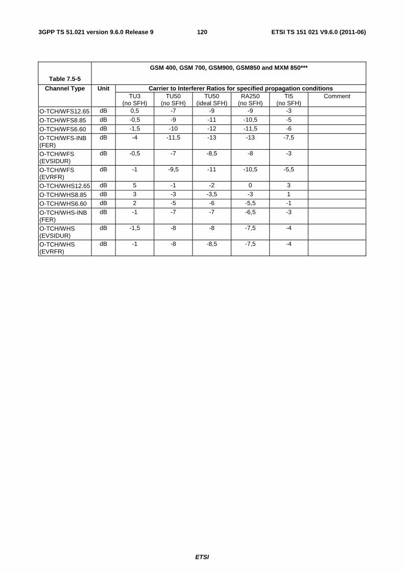
ETSI
ETSI TS 151 021 V9.6.0 (2011-06)1203GPP TS 51.021 version 9.6.0 Release 9
Table 7.5-5
GSM 400, GSM 700, GSM900, GSM850 and MXM 850***
Channel Type Unit Carrier to Interferer Ratios for specified propagation conditions TU3
(no SFH) TU50
(no SFH) TU50
(ideal SFH) RA250
(no SFH) TI5
(no SFH) Comment
O-TCH/WFS12.65 dB 0,5 -7 -9 -9 -3
O-TCH/WFS8.85 dB -0,5 -9 -11 -10,5 -5
O-TCH/WFS6.60 dB -1,5 -10 -12 -11,5 -6
O-TCH/WFS-INB (FER)
dB -4 -11,5 -13 -13 -7,5
O-TCH/WFS (EVSIDUR)
dB -0,5 -7 -8,5 -8 -3
O-TCH/WFS (EVRFR)
dB -1 -9,5 -11 -10,5 -5,5
O-TCH/WHS12.65 dB 5 -1 -2 0 3
O-TCH/WHS8.85 dB 3 -3 -3,5 -3 1
O-TCH/WHS6.60 dB 2 -5 -6 -5,5 -1
O-TCH/WHS-INB (FER)
dB -1 -7 -7 -6,5 -3
O-TCH/WHS (EVSIDUR)
dB -1,5 -8 -8 -7,5 -4
O-TCH/WHS (EVRFR)
dB -1 -8 -8,5 -7,5 -4

ETSI
ETSI TS 151 021 V9.6.0 (2011-06)1213GPP TS 51.021 version 9.6.0 Release 9
Table 7.5-5 DCS1800, PCS 1900 and MXM1900***
Channel Type Unit Carrier to Interferer Ratios for specified propagation conditions
TU1.5 (no SFH)
TU50 (no SFH)
TU50 (ideal SFH)
RA130 (no SFH)
TI5 (no SFH)
Comment
PDTCH/MCS-5 dB 2.5 -2 -1.5 1 2
PDTCH/MCS-6 dB 4.5 1.5 1.5 6.5 5
PDTCH/MCS-7 dB 8 10.5 11 13.5** 12.5
PDTCH/MCS-8 dB 10.5 10** 9.5** * 13**
PDTCH/MCS-9 dB 12 16** 16** * 17.5**
PDTCH/UAS-7 dB 13 9.5 9.5 10.5 13.5
PDTCH/UAS-8 dB 14.5 12 12 15 15
PDTCH/UAS-9 dB 15.5 15.5 15.5 22.5 17.5
PDTCH/UAS-10 dB 17.5 24.5 24.5 25** 21
PDTCH/UAS-11 dB 19 20.5** 20.5** - 27.5
PDTCH/UBS-5 dB -17.5 -13.0 -13.0 -9.0 -12.5 Input signals generated with wide
pulse-shaping filter
(Note 5)
PDTCH/UBS-6 dB -15.0 -10.0 -10.0 -5.5 -10.0
PDTCH/UBS-7 dB -11.5 -5.5 -5.5 -2.5 -5.5
PDTCH/UBS-8 dB -8.0 -2.0 -2.0 1.5 -2.0
PDTCH/UBS-9 dB -6.0 1.5 1.5 4.0 0.5
PDTCH/UBS-10 dB 0.0 5.0 5.0 12.5 5.0
PDTCH/UBS-11 dB 5.5 14.5 14.5 25.0 13.5
PDTCH/UBS-12 dB 8.0 20.0 20.0 16.5** 17.5
PDTCH/UBS-5 dB -14.5 -10.0 -10.0 -2.5 -10.0 Input signals generated
with narrow pulse-shaping
filter (Note 5)
PDTCH/UBS-6 dB -12.0 -6.5 -6.5 1.5 -7.5
PDTCH/UBS-7 dB -1.5 2.0 2.0 7.0 1.5
PDTCH/UBS-8 dB 1.0 5.0 5.0 11.0 4.5
PDTCH/UBS-9 dB 2.5 7.0 7.0 12.5 6.0
PDTCH/UBS-10 dB 7.0 14.0 14.0 18.0 13.0
PDTCH/UBS-11 dB 8.5 12.5** 12.5** 18.5** 17.0
PDTCH/UBS-12 dB 9.0 14.0** 14.0** 22.5** 18.5
E-TCH/F43,2 NT dB 8 4 3.5 14 7.5
E-TCH/F32,0 T dB 7 -3.5 -3.5 -4 1.5
E-TCH/F28,8 T dB 10 - 0.5 - 0.5 5 4.5
E-TCH/F28,8NT dB 3.5 - 2 - 2 0.5 2.5
O-FACCH/F dB 0 -6,5 0 -8,5 -3,5
O-FACCH/H dB 0,5 -5,5 0,5 -6 -1,5
O-TCH/AHS12.2 dB 5 -1 5 -0,5 3
O-TCH/AHS10.2 dB 4,5 -2 4,5 -2 2
O-TCH/AHS7.95 dB 3 -3 3 -3,5 1
O-TCH/AHS7.4 dB 2,5 -4 2,5 -4,5 0
O-TCH/AHS6.7 dB 2 -5 2 -5,5 -0,5
O-TCH/AHS5.9 dB 1,5 -5,5 1,5 -6,5 -1,5
O-TCH/AHS5.15 dB 1 -6,5 1 -7 -3
O-TCH/AHS4.75 dB 0,5 -7 0,5 -7,5 -4
O-TCH/AHS-INB (FER)
dB -1 -6,5 -1 -6,5 -3
O-TCH/AHS (EVSIDUR)
dB -1,5 -7,5 -1,5 -7,5 -4
O-TCH/AHS (EVRFR)
dB -1 -8 -1 -7,5 -4
O-TCH/WFS23.85 dB 5 -2,5 5 -4 2
O-TCH/WFS15.85 dB 2 -5,5 2 -7 -1
O-TCH/WFS12.65 dB 0,5 -7,5 0,5 -9 -3

ETSI
ETSI TS 151 021 V9.6.0 (2011-06)1223GPP TS 51.021 version 9.6.0 Release 9
Table 7.5-5 DCS1800, PCS 1900 and MXM1900***
Channel Type Unit Carrier to Interferer Ratios for specified propagation conditions
TU1.5 (no SFH)
TU50 (no SFH)
TU50 (ideal SFH)
RA130 (no SFH)
TI5 (no SFH)
Comment
O-TCH/WFS8.85 dB -0,5 -10 -0,5 -10,5 -5
O-TCH/WFS6.60 dB -1,5 -11,5 -1,5 -11,5 -6
O-TCH/WFS-INB (FER)
dB -4 -11 -4 -13 -7,5
O-TCH/WFS (EVSIDUR)
dB -0,5 -8 -0,5 -8 -3
O-TCH/WFS (EVRFR)
dB -1 -10,5 -1 -10,5 -5,5
O-TCH/WHS12.65 dB 5 -1 5 0 3
O-TCH/WHS8.85 dB 3 -3 3 -3 1
O-TCH/WHS6.60 dB 2 -5 2 -5,5 -1
O-TCH/WHS-INB (FER)
dB -1 -6,5 -1 -6,5 -3
O-TCH/WHS (EVSIDUR)
dB -1,5 -7,5 -1,5 -7,5 -4
O-TCH/WHS (EVRFR)
dB -1 -8 -1 -7,5 -4
NOTE 1: PDTCH/MCS-x and UAS-x shall not be tested for the propagation conditions marked as (*). NOTE 2: For GSM 400 the speeds shall be doubled (e.g. TU50 shall be TU100) and for GSM 700 the speeds shall be
multiplied by 1,2 (e.g. TU50 shall be TU60). NOTE 3: Performance is specified at 30% BLER for those cases marked as (**). ***NOTE 4: ECSD is not applicable for MXM850 and MXM1900. NOTE 5: PDTCH/UBS-5 to 12 requirements assume two-antenna configuration. The Interfering signal shall use higher
symbol rate and be generated with the same modulation and pulse shaping filter as the wanted signal.
Table 7.5-5a: carrier to interference ratios for channels in VAMOS mode.
Table 7.5-5a GSM 400, GSM 700, GSM900, GSM 850 and MXM 850
Channel Type Unit SCPIR_UL (dB)
Carrier to Interferer Ratios (C/I1) for test scenarios for propagation condition TU50 (no SFH)
VUTS-1 VUTS-2 VUTS-3 VUTS-4 TCH/HS dB 0 [tbd] [tbd] [tbd] [tbd]
TCH/EFS dB 0 [tbd] [tbd] [tbd] [tbd]
TCH/AFS 12.2 dB 0 [tbd] [tbd] [tbd] [tbd]
TCH/AFS 4.75 dB 0 [tbd] [tbd] [tbd] [tbd]
TCH/AHS 7.4 dB 0 [tbd] [tbd] [tbd] [tbd]
TCH/AHS 4.75 dB 0 [tbd] [tbd] [tbd] [tbd]
TCH/WFS 12.65 dB 0 [tbd] [tbd] [tbd] [tbd]
TCH/WFS 6.60 dB 0 [tbd] [tbd] [tbd] [tbd]
FACCH/F dB 0 [tbd] [tbd] [tbd] [tbd]
FACCH/H dB 0 [tbd] [tbd] [tbd] [tbd]
SACCH dB 0 [tbd] [tbd] [tbd] [tbd]
Repeated SACCH dB 0 [tbd] [tbd] [tbd] [tbd]
TCH/HS dB -10 [tbd] [tbd] [tbd] [tbd]
TCH/EFS dB -10 [tbd] [tbd] [tbd] [tbd]
TCH/AFS 12.2 dB -10 [tbd] [tbd] [tbd] [tbd]
TCH/AHS 7.4 dB -10 [tbd] [tbd] [tbd] [tbd]
TCH/WFS 12.65 dB -10 [tbd] [tbd] [tbd] [tbd]

ETSI
ETSI TS 151 021 V9.6.0 (2011-06)1233GPP TS 51.021 version 9.6.0 Release 9
Table 7.5-5a DCS1800, PCS 1900 and MXM1900
Channel Type Unit SCPIR_UL (dB)
Carrier to Interferer Ratios (C/I1) for test scenarios for propagation condition TU50 (no SFH)
VUTS-1 VUTS-2 VUTS-3 VUTS-4 TCH/HS dB 0 [tbd] [tbd] [tbd] [tbd]
TCH/EFS dB 0 [tbd] [tbd] [tbd] [tbd]
TCH/AFS 12.2 dB 0 [tbd] [tbd] [tbd] [tbd]
TCH/AFS 4.75 dB 0 [tbd] [tbd] [tbd] [tbd]
TCH/AHS 7.4 dB 0 [tbd] [tbd] [tbd] [tbd]
TCH/AHS 4.75 dB 0 [tbd] [tbd] [tbd] [tbd]
TCH/WFS 12.65 dB 0 [tbd] [tbd] [tbd] [tbd]
TCH/WFS 6.60 dB 0 [tbd] [tbd] [tbd] [tbd]
FACCH/F dB 0 [tbd] [tbd] [tbd] [tbd]
FACCH/H dB 0 [tbd] [tbd] [tbd] [tbd]
SACCH dB 0 [tbd] [tbd] [tbd] [tbd]
Repeated SACCH dB 0 [tbd] [tbd] [tbd] [tbd]
TCH/HS dB -10 [tbd] [tbd] [tbd] [tbd]
TCH/EFS dB -10 [tbd] [tbd] [tbd] [tbd]
TCH/AFS 12.2 dB -10 [tbd] [tbd] [tbd] [tbd]
TCH/AHS 7.4 dB -10 [tbd] [tbd] [tbd] [tbd]
TCH/WFS 12.65 dB -10 [tbd] [tbd] [tbd] [tbd]
NOTE 1: I1 corresponds to the power of Co-channel 1 (VUTS-1, VUTS-3 and VUTS-4) or Adjacent channel 1 (VUTS-2)
NOTE 2: For GSM 400 the speeds shall be doubled (e.g. TU50 shall be TU100) and for GSM 700 the speeds shall be multiplied by 1,2 (e.g. TU50 shall be TU60)
All TRXs in the BSS configuration shall be on and transmitting full power in all time slots.
The input signal before channel encoding in the BSSTE shall be compared with the signal which is obtained from the BSS receiver after channel decoding.
7.5.3 Essential conformance
Test Environment:
Normal.
Normal and Micro-BTS Conformance Requirement
1) Co-channel:
The error performance shall be measured for TCH/FS channel (FER, class Ib and class II), for TU50 propagation condition. If synthesizer SFH is supported by the BSS, this shall be enabled, with the range of hopping frequencies centred around RF channel M. If synthesizer SFH is not supported, this shall be tested on one ARFCN channel.
With SFH disabled, the error performance for each of the following logical channel types supported by the BSS shall be measured, each on one ARFCN, for the specified propagation conditions (for GSM 400 applicable speeds are multiplied by 2 and for GSM 700 by 1,2):

ETSI
ETSI TS 151 021 V9.6.0 (2011-06)1243GPP TS 51.021 version 9.6.0 Release 9
TCH/FS: TU1.5 or TU3
FACCH/F: TU1.5 or TU3
FACCH/H: TU1.5 or TU3
E-FACCH/F: TU1.5 or TU3
SDCCH: TU1.5 or TU3
TCH/F9.6: TU1.5 or TU3, TU50
TCH/F4.8: TU1.5 or TU3, TU50
PDTCH/CS-1: TU1.5 or TU3, TU50
PDTCH/MCS-1 or, if not supported, for the PDTCH/MCS-x with the
next higher supported number x: TU1.5 or TU3, TU50
PDTCH/MCS-5 or, if not supported, PDTCH/MCS-x with the
next higher supported number x: TU1.5 or TU3, TU50
E-TCH/43,2 NT or for the highest supported data speed: TU1.5 or TU3, TU50
PDTCH/UAS-7 or, if not supported, PDTCH/UAS-x with the
next higher supported number x: TU1.5 or TU3, TU50
PDTCH/UBS-5 or, if not supported, PDTCH/UBS-x with the
next higher supported number x: TU1.5 or TU3, TU50
PDTCH/UBS-7 or, if not supported, PDTCH/UBS-x with the
next higher supported number x: TU1.5 or TU3, TU50
PDTCH/UBS-10 or, if not supported, PDTCH/UBS-x with the
next higher supported number x: TU1.5 or TU3, TU50
If AMR or AMR-WB is supported by the BSS, the error performance given in tables 7.5-6 and 7.5-7 shall be met for one channel under TU50 (no SFH) propagation condition. The channel with the highest bitrate shall be tested.
If 8-PSK modulated AMR or AMR-WB is supported by the BSS, the error performance given in tables 7.5-6 and 7.5-7 shall be met for one traffic channel and corresponding associated control channel O-FACCH under TU50 (no SFH) propagation condition. The traffic channel with the highest bitrate shall be tested.
2) 200 kHz offset:
With SFH disabled, the error performance for each of the following logical channel types supported by the BSS shall be measured, each on one ARFCN, for the specified propagation conditions:
TCH/FS: TU50
FACCH/F: TU50

ETSI
ETSI TS 151 021 V9.6.0 (2011-06)1253GPP TS 51.021 version 9.6.0 Release 9
E-TCH/43,2 NT or for the highest supported data speed or PDTCH/MCS-5 or, if not supported, PDTCH/MCS-x with the next higher supported number x: TU50
PDTCH/UAS-7 or, if not supported, PDTCH/UAS-x with the next higher supported number x TU50
PDTCH/UBS-5 or, if not supported PDTCH/UBS-x with the next higher supported number x TU50
PDTCH/UBS-7 or, if not supported PDTCH/UBS-x with the next higher supported number x TU50
PDTCH/UBS-10 or, if not supported PDTCH/UBS-x with the next higher supported number x TU50
For tests with UBS-x, the Interfering signal shall use higher symbol rate and be generated with the same modulation and pulse shaping filter as the wanted signal.
3) 400 kHz offset:
With SFH disabled, the error performance for each of the following logical channel types supported by the BSS shall be measured, each on RF channels B, M and T, for the specified propagation conditions:
TCH/FS: TU50
E-TCH/43,2 NT or for the highest supported data speed or PDTCH/MCS-5 or, if not supported, PDTCH/MCS-x with the
next higher supported number x: TU50
PDTCH/UAS-7 or, if not supported, PDTCH/UAS-x with the next higher supported number x TU50
PDTCH/UBS-5 or, if not supported PDTCH/UBS-x with the next higher supported number x TU50
PDTCH/UBS-7 or, if not supported PDTCH/UBS-x with the next higher supported number x TU50
PDTCH/UBS-10 or, if not supported PDTCH/UBS-x with the next higher supported number x TU50
With SFH disabled, the error performance for each of the following logical channel types supported by the BSS shall be measured, each on one ARFCN, for the specified propagation profiles:
FACCH/F: TU50
In cases 1) and 2) above, the error performance given in tables 7.5-6 and 7.5-7 shall be met for all combinations of logical channel type, frequency of wanted signal, 0kHz and 200kHz frequency offset of interfering signal and multipath propagation condition tested. For 8-PSK modulated AMR and AMR-WB channels 200 kHz offset table 7.5-8 applies.
In case 3) above, the error performance given in tables 7.5-6 and 7.5-7 for EGPRS, ECSD and AMR-WB, and 8-PSK modulated AMR and AMR-WB channels and tables 7.5-9 and 7.5-10 for other channels shall be met for all combinations of logical channel type, frequency of wanted signal, 400kHz frequency offset of interfering signal and multipath propagation condition tested.
The value of α in tables 7.5-6, 7.5-7, 7.5-9 and 7.5-10 shall be in the range 1 to 1.6, and shall be the same for both occurrences in each propagation condition; it may be different for different propagation conditions.
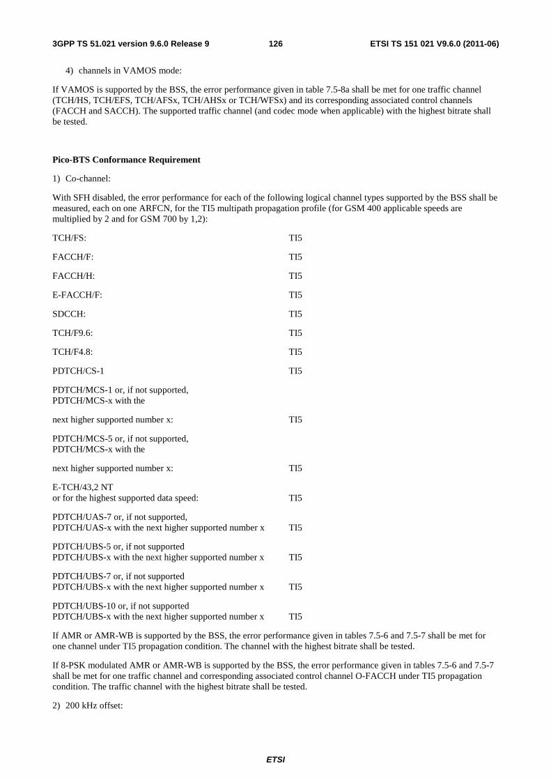
ETSI
ETSI TS 151 021 V9.6.0 (2011-06)1263GPP TS 51.021 version 9.6.0 Release 9
4) channels in VAMOS mode:
If VAMOS is supported by the BSS, the error performance given in table 7.5-8a shall be met for one traffic channel (TCH/HS, TCH/EFS, TCH/AFSx, TCH/AHSx or TCH/WFSx) and its corresponding associated control channels (FACCH and SACCH). The supported traffic channel (and codec mode when applicable) with the highest bitrate shall be tested.
Pico-BTS Conformance Requirement
1) Co-channel:
With SFH disabled, the error performance for each of the following logical channel types supported by the BSS shall be measured, each on one ARFCN, for the TI5 multipath propagation profile (for GSM 400 applicable speeds are multiplied by 2 and for GSM 700 by 1,2):
TCH/FS: TI5
FACCH/F: TI5
FACCH/H: TI5
E-FACCH/F: TI5
SDCCH: TI5
TCH/F9.6: TI5
TCH/F4.8: TI5
PDTCH/CS-1 TI5
PDTCH/MCS-1 or, if not supported, PDTCH/MCS-x with the
next higher supported number x: TI5
PDTCH/MCS-5 or, if not supported, PDTCH/MCS-x with the
next higher supported number x: TI5
E-TCH/43,2 NT or for the highest supported data speed: TI5
PDTCH/UAS-7 or, if not supported, PDTCH/UAS-x with the next higher supported number x TI5
PDTCH/UBS-5 or, if not supported PDTCH/UBS-x with the next higher supported number x TI5
PDTCH/UBS-7 or, if not supported PDTCH/UBS-x with the next higher supported number x TI5
PDTCH/UBS-10 or, if not supported PDTCH/UBS-x with the next higher supported number x TI5
If AMR or AMR-WB is supported by the BSS, the error performance given in tables 7.5-6 and 7.5-7 shall be met for one channel under TI5 propagation condition. The channel with the highest bitrate shall be tested.
If 8-PSK modulated AMR or AMR-WB is supported by the BSS, the error performance given in tables 7.5-6 and 7.5-7 shall be met for one traffic channel and corresponding associated control channel O-FACCH under TI5 propagation condition. The traffic channel with the highest bitrate shall be tested.
2) 200 kHz offset:

ETSI
ETSI TS 151 021 V9.6.0 (2011-06)1273GPP TS 51.021 version 9.6.0 Release 9
With SFH disabled, the error performance for each of the following logical channel types supported by the BSS shall be measured, each on one ARFCN, for the TI5 multipath propagation profile:
TCH/FS: TI5
FACCH/F: TI5
E-TCH/43,2 NT or for the highest supported data speed or PDTCH/MCS-5 or, if not supported, PDTCH/MCS-x with the next
higher supported number x: TI5
PDTCH/UAS-7 or, if not supported, PDTCH/UAS-x with the next higher supported number x TI5
PDTCH/UBS-5 or, if not supported PDTCH/UBS-x with the next higher supported number x TI5
PDTCH/UBS-7 or, if not supported PDTCH/UBS-x with the next higher supported number x TI5
PDTCH/UBS-10 or, if not supported PDTCH/UBS-x with the next higher supported number x TI5
3) 400 kHz offset:
With SFH disabled, the error performance for each of the following logical channel types supported by the BSS shall be measured, each on one ARFCN, for the TI5 multipath propagation profile:
TCH/FS: TI5
FACCH/F: TI5
E-TCH/43,2 NT or for the highest supported data speed or PDTCH/MCS-5 or, if not supported, PDTCH/MCS-x with the next
higher supported number x: TI5
PDTCH/UAS-7 or, if not supported, PDTCH/UAS-x with the next higher supported number x TI5
PDTCH/UBS-5 or, if not supported PDTCH/UBS-x with the next higher supported number x TI5
PDTCH/UBS-7 or, if not supported PDTCH/UBS-x with the next higher supported number x TI5
PDTCH/UBS-10 or, if not supported PDTCH/UBS-x with the next higher supported number x TI5
In cases 1) and 2) above, the error performance given in tables 7.5-6 and 7.5-7 shall be met for all combinations of logical channel type, frequency of wanted signal, 0kHz and 200kHz frequency offset of interfering signal and TI5 multipath propagation condition tested. For 8-PSK modulated AMR and AMR-WB channels 200 kHz offset table 7.5-8 applies.
In case 3) above, the error performance given in tables 7.5-6 and 7.5-7 for EGPRS, ECSD and AMR-WB channels and tables 7.5-9 and 7.5-10 for other channels shall be met for all combinations of logical channel type, frequency of wanted signal, 400kHz frequency offset of interfering signal and multipath propagation condition tested.
The value of α in tables 7.5-6, 7.5-7, 7.5-9 and 7.5-10 shall be in the range 1 to 1.6, and shall be the same for both occurrences in the TI5 propagation condition.
VAMOS mode is not applicable to pico BTS.

ETSI
ETSI TS 151 021 V9.6.0 (2011-06)1283GPP TS 51.021 version 9.6.0 Release 9
7.5.4 Complete conformance
Test Environment:
Normal.
Normal and Micro-BTS Conformance Requirement
The error performance of any logical channel type supported by the BSS for any multipath propagation condition (excluding TI5) given in tables 7.5-6, 7.5-7, 7.5-9 and 7.5-10 shall not be worse than the error ratios given in tables 7.5-6, 7.5-7, 7.5-9 and 7.5-10 with the exception that for EGPRS, EGPRS2, ECSD and AMR-WB, and 8-PSK modulated AMR and AMR-WB channels the requirements in tables 7.5-6 and 7.5-7 apply. For 8-PSK modulated AMR and AMR-WB channels 200 kHz offset table 7.5-8 applies. For the circuit switched control channels not listed in tables 7.5-6, 7.5-7, 7.5-9 and 7.5-10 the requirements for the SDCCH shall apply. The requirements for propagation conditions with ideal SFH shall only apply if SFH is supported by the BSS. For channels in VAMOS mode, table 7.5-8a applies.
For the propagation conditions with ideal SFH, the tests shall be performed with the range of hopping frequencies centred around RF channel M. For propagation conditions with no SFH, the tests shall be performed at the RF channels B, M, and T.
The value of α in tables 7.5-6, 7.5-7, 7.5-9 and 7.5-10 shall be in the range 1 to 1.6, and shall be the same for both occurrences in each propagation condition; it may be different for different propagation conditions.
NOTE 1: For TU50 (ideal FH), sufficient decorrelation may be achieved with 4 frequencies spaced over 5 MHz.
Pico-BTS Conformance Requirement
The error performance of any logical channel type for the TI5 multipath propagation condition shall not be worse than the error ratios given in tables 7.5-6, 7.5-7, 7.5-9 and 7.5-10. The tests shall be performed with SFH disabled, at the RF channels B, M, and T. The value of α in tables 7.5-6, 7.5-7, 7.5-9 and 7.5-10 shall be in the range 1 to 1.6, and shall be the same for both occurrences in the TI5 propagation condition.

ETSI
ETSI TS 151 021 V9.6.0 (2011-06)1293GPP TS 51.021 version 9.6.0 Release 9
Table 7.5-6: Multipath error performance limits at RX interference level
Table 7.5-6 GSM 400, GSM 700, GSM900, GSM 850 and MXM 850
Channel Type Error Measure Error Ratios for the specified propagation conditions TU3
(no SFH) TU50
(no SFH) TU50
(ideal SFH) RA250
(no SFH) TI5
(no SFH) FACCH/H (FER) 22 % 6.7 % 6.7 % 5.7 % 6.7 %
FACCH/F (FER) 22 % 9.5 % 3.4 % 3.5 % 9.5 %
E-FACCH/F (FER) 5 % 5 % 5 % 5 % 5 %
SDCCH & SACCH (FER) 22 % (*) 13 % 9 % 8.0 % 13 %
SACCH (TCH/AxS) (FER @-3 dB) 40 % (*) - - - -
RACH (FER) 15 % 16 % 16 % 13 % 16 %
E-TCH/F43,2 NT (BLER) 10 % 10 % 10 % 10 % 10 %
E-TCH/F32,0 T (BER) 0.1 % 0.1 % 0.1 % 0.1 % 0.1 %
E-TCH/F28,8 T (BER) 0.1 % 0.1 % 0.1 % 0.1 % 0.1 %
E-TCH/F28,8 NT (BLER) 10 % 10 % 10 % 10 % 10 %
TCH/F14.4 (BER) 10.0% 4.5% 3.0% 3.0% 4.5 %
TCH/F9.6 (BER) 8.0 % 0.80 % 0.30 % 0.2 % 0.80 %
TCH/F4.8 (BER) 3.0 % 10-4 10-4 10-4 10-4 TCH/F2.4 (BER) 3.0 % 10-4 10-5 10-5 10-4 TCH/H4.8 (BER) 8.0 % 0.80 % 0.30 % 0.20 % 0.80 %
TCH/H2.4 (BER) 4.0 % 2 10-4 10-4 10-4 2 10-4 TCH/FS (FER) 21α % 6.0α % 3.0α % 3.0α % 6.0α %
- class Ib (RBER) 2.0/α % 0.40/α % 0.20/α % 0.20/α % 0.40/α %
- class II (RBER) 4.0 % 8.0 % 8.0 % 8.0 % 8.0 %
TCH/HS (FER) 19.1 % 5.0 % 5.0 % 4.7 % 5.0 %
- class Ib (RBER, BFI=0) 0.52 % 0.29 % 0.29 % 0.21 % 0.29 %
- class II (RBER, BFI=0) 2.8 % 7.1 % 7.1 % 7.0 % 7.1 %
- (UFR) 20.7 % 6.1 % 6.1 % 5.6 % 6.1 %
- class Ib (RBER, UFI=0) 0.29 % 0.21 % 0.21 % 0.17 % 0.21 %
- (EVSIDR) 21.9 % 7.0 % 7.0 % 6.3 % 7.0 %
- (RBER, SID=2 and BFI=0)
0.02 % 0.01 % 0.01 % 0.01 % 0.01 %
- (ESIDR) 17.1 % 3.6 % 3.6 % 3.4 % 3.6 %
- (RBER, SID=1 or 2) 0.50 % 0.26 % 0.26 % 0.20 % 0.26 %
TCH/EFS (FER) 23 % 9 % 3 % 4 % 9 % - class Ib (RBER) 0.20 % 0.20 % 0.10 % 0.13 % 0.20 % - class II (RBER) 3 % 7 % 8 % 8 % 7 % TCH/AFS12.2 (FER) 22 % 6 % 3,5 % 2,5 % 6 % - Class Ib (RBER) 0,9 % 1,7 % 1,7 % 1,5 % 1,7 % TCH/AFS10.2 (FER) 18 % 2,7 % 1,4 % 0,92 % 2,7 % - Class Ib (RBER) 0,53 % 0,3 % 0,21 % 0,16 % 0,3 % TCH/AFS7.95 (FER) 13 % (*) 0,51 % 0,12 % 0,073 % 0,51 % - Class Ib (RBER) 0,66 % (*) 0,15 % 0,065 % 0,044 % 0,15 % TCH/AFS7.95 (FER@-3dB) 26 % (*) 5,3 % 2,7 % 1,8 % 5,3 % - Class Ib (RBER@-3dB) 1,2 % (*) 1 % 0,78 % 0,6 % 1 % TCH/AFS7.4 (FER) 14 % (*) 0,56 % 0,16 % 0,09 % 0,56 % - Class Ib (RBER) 0,43 % (*) 0,072 % 0,032 % 0,018 % 0,072 % TCH/AFS7.4 (FER@-3dB) 26 % (*) 5,4 % 3,1 % 2 % 5,4 % - Class Ib (RBER@-3dB) 0,79 % (*) 0,52 % 0,38 % 0,28 % 0,52 % TCH/AFS6.7 (FER) 11 % (*) 0,21 % 0,041 % 0,021 % 0,21 % - Class Ib (RBER) 0,75 % (*) 0,11 % 0,042 % 0,028 % 0,11 % TCH/AFS6.7 (FER@-3dB) 23 % (*) 2,9 % 1,2 % 0,75 % 2,9 % - Class Ib (RBER@-3dB) 1,4 % (*) 0,86 % 0,6 % 0,44 % 0,86 % TCH/AFS5.9 (FER) 10 % (*) 0,12 % 0,018 % 0,01 % 0,12 % - Class Ib (RBER) 0,38 % (*) 0,022 % 0,005 % 0,003 % 0,022 % TCH/AFS5.9 (FER@-3dB) 21 % (*) 2 % 0,7 % 0,4 % 2 % - Class Ib (RBER@-3dB) 0,74 % (*) 0,23 % 0,12 % 0,079 % 0,23 %

ETSI
ETSI TS 151 021 V9.6.0 (2011-06)1303GPP TS 51.021 version 9.6.0 Release 9
Table 7.5-6 GSM 400, GSM 700, GSM900, GSM 850 and MXM 850
Channel Type Error Measure Error Ratios for the specified propagation conditions TU3
(no SFH) TU50
(no SFH) TU50
(ideal SFH) RA250
(no SFH) TI5
(no SFH) TCH/AFS5.15 (FER) 9,2 % (*) 0,081 % 0,011 % 0,01 % 0,081 % - Class Ib (RBER) 0,44 % (*) 0,019 % 0,003 % 0,002 % 0,019 % TCH/AFS5.15 (FER@-3dB) 19 % (*) 1,4 % 0,47 % 0,25 % 1,4 % - Class Ib (RBER@-3dB) 0,85 % (*) 0,22 % 0,11 % 0,069 % 0,22 % TCH/AFS4.75 (FER) 7,9 % (*) 0,036 % 0,01 % 0,01 % 0,036 % - Class Ib (RBER) 0,32 % (*) 0,006 % 0,001 % 0,001 % 0,006 % TCH/AFS4.75 (FER@-3dB) 17 % (*) 0,82 % 0,23 % 0,11 % 0,82 % - Class Ib (RBER@-3dB) 0,62 % (*) 0,11 % 0,033 % 0,019 % 0,11 % TCH/AFS-INB (FER) 1,5 % (*) 0,025 % 0,018 % 0,009 % 0,025 % TCH/AFS-INB (FER@-3dB) 3,5 % (*) 0,22 % 0,16 % 0,1 % 0,22 % TCH/AFS (EVSIDUR) 11 % (*) 1,4 % (*) 0,39 % (*) 0,46 % (*) 1,4 % (*) TCH/AFS (EVSIDUR@-3dB) 21 % (*) 6.3 % (*) 3,4 % (*) 3,1 % (*) 6.3 % (*) TCH/AFS (EVRFR) 10 % (*) 0,15 % 0,024 % 0,01 % 0,15 % TCH/AFS (EVRFR@-3dB) 21 % (*) 2,08 % 0,77 % 0,48 % 2,08 % TCH/AHS7.95 (FER) 27 % 22 % 22 % 21 % 22 % - Class Ib (RBER) 0,84 % 2,3 % 2,3 % 2,1 % 2,3 % - Class II (RBER) 1,7 % 5,3 % 5,3 % 5 % 5,3 % TCH/AHS7.95 (FER@+3dB) 14 % 6,7 % 6.7 % 7 % 6,7 % - Class Ib (RBER@+3dB) 0,48 % 1 % 1 % 1 % 1 % - Class II (RBER@+3dB) 1 % 3,2 % 3,2 % 3,2 % 3,2 % TCH/AHS7.4 (FER) 25 % 18 % 18 % 17 % 18 % - Class Ib (RBER) 0,68 % 1,4 % 1,4 % 1,3 % 1,4 % - Class II (RBER) 1,9 % 5,6 % 5,6 % 5,4 % 5,6 % TCH/AHS7.4 (FER@+3dB) 13 % 4,8 % 4.8 % 5,3 % 4,8 % - Class Ib (RBER@+3dB) 0,38 % 0,51 % 0,51 % 0,50 % 0,51 % - Class II (RBER@+3dB) 1,2 % 3,3 % 3,3 % 3,4 % 3,3 % TCH/AHS6.7 (FER) 23 % 11 % 11 % 11 % 11 % - Class Ib (RBER) 0,71 % 1,2 % 1,2 % 1,1 % 1,2 % - Class II (RBER) 2,3 % 6,2 % 6,2 % 6 % 6,2 % TCH/AHS6.7 (FER@+3dB) 11 % 2,3 % 2,3 % 2,9 % 2,3 % - Class Ib (RBER@+3dB) 0,39 % 0,39 % 0,39 % 0,4 % 0,39 % - Class II (RBER@+3dB) 1,4 % 3,6 % 3,6 % 3,6 % 3,6 % TCH/AHS5.9 (FER) 21 % 7,1 % 7,1 % 7 % 7,1 % - Class Ib (RBER) 0,55 % 0,57 % 0,57 % 0,51 % 0,57 % - Class II (RBER) 2,6 % 6,5 % 6,5 % 6,3 % 6,5 % TCH/AHS5.15 (FER) 17 % 3,3 % 3,3 % 3,5 % 3,3 % - Class Ib (RBER) 0,8 % 0,6 % 0,6 % 0,57 % 0,6 % - Class II (RBER) 3,1 % 6,9 % 6,9 % 6,7 % 6,9 % TCH/AHS4.75 (FER) 15 % 1,8 % 1,8 % 2,1 % 1,8 % - Class Ib (RBER) 0,6 % 0,22 % 0,22 % 0,22 % 0,22 % - Class II (RBER) 3,6 % 7 % 7 % 6,9 % 7 % TCH/AHS-INB (FER) 2,7 % (*) 0,7 % (*) 0,7 % (*) 0,63 % (*) 0,7 % (*) TCH/AHS-INB (FER@-3dB) 6 % (*) 2,2 % (*) 2,2 % (*) 2 % (*) 2,2 % (*) TCH/AHS (EVSIDUR) 15 % (*) 2,5 % (*) 2,5 % (*) 3,8 % (*) 2,5 % (*) TCH/AHS (EVSIDUR@-3dB) 28 % (*) 15 % (*) 15 % (*) 15 % (*) 15 % (*) TCH/AHS (EVRFR) 11 % (*) 0,51 % (*) 0,51 % (*) 0,61 % (*) 0,51 % (*) TCH/AHS (EVRFR@-3dB) 22 % (*) 4,4 % (*) 4,4 % (*) 4,1 % (*) 4,4 % (*) PDTCH/CS-1 to 4 (BLER) 10% 10% 10% 10% 10 % PDTCH/MCS-1 to 6 (BLER) 10% 10% 10% 10% 10% PDTCH/MCS-7 (BLER) 10 % 10 % 10 % 30 % 10 % PDTCH/MCS-8 (BLER) 10 % 10%/30 %* 10%/30 %* - 30 % PDTCH/MCS-9 (BLER) 10 % 10%/30 %* 10%/30 %* - 30 % PDTCH/UAS-7 to 9 (BLER) 10% 10% 10% 10% 10% PDTCH/UAS-10 (BLER) 10% 10% 10% 30% 10% PDTCH/UAS-11 (BLER) 10% 10% 10% - 10% PDTCH/UBS-5 to 10 (BLER) 10% 10% 10% 10% 10% PDTCH/UBS-11 (BLER) 10% 10% 10% 10% 4) 10% PDTCH/UBS-12 (BLER) 10% 10% 10% 30% 10% PRACH/11 bit (BLER) 15% 15% 15% 15% 15 %

ETSI
ETSI TS 151 021 V9.6.0 (2011-06)1313GPP TS 51.021 version 9.6.0 Release 9
Table 7.5-6 GSM 400, GSM 700, GSM900, GSM 850 and MXM 850
Channel Type Error Measure Error Ratios for the specified propagation conditions TU3
(no SFH) TU50
(no SFH) TU50
(ideal SFH) RA250
(no SFH) TI5
(no SFH) PRACH/8 bit (BLER) 15% 15% 15% 15% 15 % PACCH (BLER) 10% 10% 10% 10% 10 % TCH/WFS12.65 (FER) 1% 1% 1% 1% 1% (RBER) 0,08 % 0,40 % 0,63 % 0,63 % 0,40 % TCH/ WFS8.85 (FER) 1% 1% 1% 1% 1% (RBER) 0,11 % 0,42 % 0,64 % 0,73 % 0,42 % TCH/ WFS6.60 (FER) 1% 1% 1% 1% 1% (RBER) 0,09 % 0,16 % 0,27 % 0,24 % 0,16 % O-FACCH/F (FER) 5 % 5 % 5 % 5 % 5 %
O-FACCH/H (FER) 5 % 5 % 5 % 5 % 5 %
O-TCH/AHS12.2 (FER) 1 % 1 % 1 % 1 % 1 %
- class Ib (RBER) 0,17 % 0,30 % 0,32 % 0,26 % 0,30 %
O-TCH/AHS10.2 (FER) 1 % 1 % 1 % 1 % 1 %
- class Ib (RBER) 0,09 % 0,15 % 0,16 % 0,20 % 0,15 %
O-TCH/AHS7.95 (FER) 1 % 1 % 1 % 1 % 1 %
- class Ib (RBER) 0,06 % 0,06 % 0,07 % 0,10 % 0,06 %
O-TCH/AHS7.4 (FER) 1 % 1 % 1 % 1 % 1 %
- class Ib (RBER) 0,08 % 0,12 % 0,13 % 0,16 % 0,12 %
O-TCH/AHS6.7 (FER) 1 % 1 % 1 % 1 % 1 %
- class Ib (RBER) 0,09 % 0,12 % 0,14 % 0,20 % 0,12 %
O-TCH/AHS5.9 (FER) 1 % 1 % 1 % 1 % 1 %
- class Ib (RBER) 0,11 % 0,16 % 0,18 % 0,17 % 0,16 %
O-TCH/AHS5.15 (FER) 1 % 1 % 1 % 1 % 1 %
- class Ib (RBER) 0,06 % 0,08 % 0,09 % 0,09 % 0,08 %
O-TCH/AHS4.75 (FER) 1 % 1 % 1 % 1 % 1 %
- class Ib (RBER) 0,08 % 0,09 % 0,10 % 0,13 % 0,09 %
O-TCH/AHS-INB (FER) 0.5 % 0.5 % 0.5 % 0.5 % 0.5 %
O-TCH/AHS (EVSIDUR) 1 % 1 % 1 % 1 % 1 %
O-TCH/AHS (EVRFR) 1 % 1 % 1 % 1 % 1 %
O-TCH/WFS23.85 (FER) 1 % 1 % 1 % 1 % 1 %
- class Ib (RBER) 0,10 % 0,15 % 0,23 % 0,28 % 0,15 %
O-TCH/WFS15.85 (FER) 1 % 1 % 1 % 1 % 1 %
- class Ib (RBER) 0,26 % 0,35 % 0,60 % 0,60 % 0,35 %
O-TCH/WFS12.65 (FER) 1 % 1 % 1 % 1 % 1 %
- class Ib (RBER) 0,18 % 0,31 % 0,45 % 0,40 % 0,31 %
O-TCH/WFS8.85 (FER) 1 % 1 % 1 % 1 % 1 %
- class Ib (RBER) 0,16 % 0,22 % 0,40 % 0,42 % 0,22 %
O-TCH/WFS6.60 (FER) 1 % 1 % 1 % 1 % 1 %
- class Ib (RBER) 0,10 % 0,14 % 0,18 % 0,23 % 0,14 %
O-TCH/WFS-INB (FER) 0.5 % 0.5 % 0.5 % 0.5 % 0.5 %
O-TCH/WFS (EVSIDUR) 1 % 1 % 1 % 1 % 1 %
O-TCH/WFS (EVRFR) 1 % 1 % 1 % 1 % 1 %
O-TCH/WHS12.65 (FER) 1 % 1 % 1 % 1 % 1 %
- class Ib (RBER) 0,16 % 0,27 % 0,36 % 0,32 % 0,27 %
O-TCH/WHS8.85 (FER) 1 % 1 % 1 % 1 % 1 %
- class Ib (RBER) 0,07 % 0,11 % 0,11 % 0,11 % 0,11 %
O-TCH/WHS6.60 (FER) 1 % 1 % 1 % 1 % 1 %
- class Ib (RBER) 0,09 % 0,12 % 0,13 % 0,14 % 0,12 %
O-TCH/WHS-INB (FER) 0.5 % 0.5 % 0.5 % 0.5 % 0.5 %
O-TCH/WHS (EVSIDUR) 1 % 1 % 1 % 1 % 1 %
O-TCH/WHS (EVRFR) 1 % 1 % 1 % 1 % 1 %

ETSI
ETSI TS 151 021 V9.6.0 (2011-06)1323GPP TS 51.021 version 9.6.0 Release 9
Table 7.5-6 GSM 400, GSM 700, GSM900, GSM 850 and MXM 850
Channel Type Error Measure Error Ratios for the specified propagation conditions TU3
(no SFH) TU50
(no SFH) TU50
(ideal SFH) RA250
(no SFH) TI5
(no SFH) * Co-channel interference performance is defined at 10% BLER and adjacent channel interference performance at 30% BLER.
NOTE 1: For GSM 400 the speeds shall be doubled (e.g. TU50 shall be TU100) and for GSM 700 the speeds shall be multiplied by 1,2 (e.g. TU50 shall be TU60).
NOTE 3: The performance requirements for inband signalling, SID_UPDATE and RATSCCH are the same as those given for TCH/AFS. It is sufficient to test inband signalling, SID_UPDATE and RATSCCH requirements for only one of the channel types TCH/AFS and TCH/WFS.
NOTE 4: 30% BLER requirement apply for wanted signal narrow.

ETSI
ETSI TS 151 021 V9.6.0 (2011-06)1333GPP TS 51.021 version 9.6.0 Release 9
Table 7.5-7: Multipath error performance limits at RX interference level
Table 7.5-7 DCS1800, PCS 1900 and MXM 1900
Channel Type Error Measure Error Ratios for the specified propagation conditions TU1.5
(no SFH) TU50
(no SFH) TU50
(ideal SFH) RA130
(no SFH) TI5
(no SFH) FACCH/H (FER) 22 % 6.9 % 6.9 % 5.7 % 6.7 %
FACCH/F (FER) 22 % 3.4 % 3.4 % 3.5 % 9.5 %
E-FACCH/F (FER) 5 5 % 5 % 5 % 5 %
SDCCH & SACCH (FER) 22 % (*) 9.0 % 9.0 % 8.0 % 13 %
SACCH (TCH/AxS) (FER @-3 dB) 40 % (*) - - - -
RACH (FER) 15 % 16 % 16 % 13 % 16 %
E-TCH/F43,2 NT (BLER) 10 % 10 % 10 % 10 % 10 %
E-TCH/F32,0 T (BER) 0.1 % 0.1 % 0.1 % 0.1 % 0.1 %
E-TCH/F28,8 T (BER) 0.1 % 0.1 % 0.1 % 0.1 % 0.1 %
E-TCH/F28,8 NT (BLER) 10 % 10 % 10 % 10 % 10 %
TCH/14.4 (BER) 10.0% 4.0% 3.1% 3.0% 4.5 %
TCH/F9.6 (BER) 8.0 % 0.80 % 0.30 % 0.2 % 0.80 %
TCH/F4.8 (BER) 3.0 % 10-4 10-4 10-4 10-4 TCH/F2.4 (BER) 3.0 % 10-5 10-5 10-5 10-4 TCH/H4.8 (BER) 8.0 % 0.80 % 0.30 % 0.20 % 0.80 %
TCH/H2.4 (BER) 4.0 % 10-4 10-4 10-4 2 10-4 TCH/FS (FER) 21α % 3.0α % 3.0α % 3.0α % 6.0α %
- class Ib (RBER) 2.0/α% 0.25/α % 0.25/α % 0.20/α % 0.40/α %
- class II (RBER) 4.0 % 8.1 % 8.1 % 8.0 % 8.0 %
TCH/HS (FER) 19.1 % 5.0 % 5.0 % 4.7 % 5.0 %
- class Ib (RBER, BFI=0) 0.52 % 0.29 % 0.29 % 0.21 % 0.29 %
- class II (RBER, BFI=0) 2.8 % 7.2 % 7.2 % 7.0 % 7.1 %
- (UFR) 20.7 % 6.1 % 6.1 % 5.6 % 6.1 %
- class Ib (RBER, UFI=0) 0.29 % 0.21 % 0.21 % 0.17 % 0.21 %
- (EVSIDR) 21.9 % 7.0 % 7.0 % 6.3 % 7.0 %
- (RBER, SID=2 and BFI=0)
0.02 % 0.01 % 0.01 % 0.01 % 0.01 %
- (ESIDR) 17.1 % 3.6 % 3.6 % 3.4 % 3.6 %
- (RBER, SID=1 or 2) 0.50 % 0.26 % 0.26 % 0.20 % 0.26 %
TCH/EFS (FER) 23 % 3 % 3 % 4 % 9 % - class Ib (RBER) 0.20 % 0.10 % 0.10 % 0.13 % 0.20 % - class II (RBER) 3 % 8 % 8 % 8 % 7 % TCH/AFS12.2 (FER) 22 % 2,7 % 2,7 % 1,8 % 6 % - Class Ib (RBER) 0,92 % 1,6 % 1,6 % 1,4 % 1,7 % TCH/AFS10.2 (FER) 18 % 0,98 % 0,98 % 0,56 % 2,7 % - Class Ib (RBER) 0,54 % 0,17 % 0,17 % 0,12 % 0,3 % TCH/AFS7.95 (FER) 13 % (*) 0,07 % 0,07 % 0,029 % 0,51 % - Class Ib (RBER) 0,67 % (*) 0,042 % 0,042 % 0,03 % 0,15 % TCH/AFS7.95 (FER@-3dB) 25 % (*) 2 % 2 % 1,2 % 5,3 % - Class Ib (RBER@-3dB) 1,2 % (*) 0,68 % 0,68 % 0,48 % 1 % TCH/AFS7.4 (FER) 14 % (*) 0,083 % 0,083 % 0,047 % 0,56 % - Class Ib (RBER) 0,43 % (*) 0,02 % 0,02 % 0,012 % 0,072 % TCH/AFS7.4 (FER@-3dB) 26 % (*) 2,3 % 2,3 % 1,4 % 5,4 % - Class Ib (RBER@-3dB) 0,8 % (*) 0,32 % 0,32 % 0,22 % 0,52 % TCH/AFS6.7 (FER) 11 % (*) 0,025 % 0,025 % 0,01 % 0,21 % - Class Ib (RBER) 0,76 % (*) 0,028 % 0,028 % 0,016 % 0,11 % TCH/AFS6.7 (FER@-3dB) 22 % (*) 0,82 % 0,82 % 0,41 % 2,9 % - Class Ib (RBER@-3dB) 1,4 % (*) 0,51 % 0,51 % 0,34 % 0,86 % TCH/AFS5.9 (FER) 10 % (*) 0,01 % 0,01 % 0,01 % 0,12 % - Class Ib (RBER) 0,38 % (*) 0,002 % 0,002 % 0,001 % 0,022 % TCH/AFS5.9 (FER@-3dB) 21 % (*) 0,41 % 0,41 % 0,2 % 2 % - Class Ib (RBER@-3dB) 0,72 % (*) 0,079 % 0,079 % 0,046 % 0,23 %
ETSI
ETSI TS 151 021 V9.6.0 (2011-06)1343GPP TS 51.021 version 9.6.0 Release 9
Table 7.5-7 DCS1800, PCS 1900 and MXM 1900
Channel Type Error Measure Error Ratios for the specified propagation conditions TU1.5
(no SFH) TU50
(no SFH) TU50
(ideal SFH) RA130
(no SFH) TI5
(no SFH) TCH/AFS5.15 (FER) 9,2 % (*) 0,01 % 0,01 % 0,01 % 0,081 % - Class Ib (RBER) 0,45 % (*) 0,001 % 0,001 % 0,001 % 0,019 % TCH/AFS5.15 (FER@-3dB) 19 % (*) 0,26 % 0,26 % 0,13 % 1,4 % - Class Ib (RBER@-3dB) 0,84 % (*) 0,072 % 0,072 % 0,038 % 0,22 % TCH/AFS4.75 (FER) 7,9 % (*) 0,01 % 0,01 % - 0,036 % - Class Ib (RBER) 0,31 % (*) 0,001 % 0,001 % 0,001 % 0,006 % TCH/AFS4.75 (FER@-3dB) 17 % (*) 0,1 % 0,1 % 0,051 % 0,82 % - Class Ib (RBER@-3dB) 0,61 % (*) 0,021 % 0,021 % 0,009 % 0,11 % TCH/AFS-INB (FER) 1,5 % (*) 0,013 % 0,013 % 0,008 % 0,025 % TCH/AFS-INB (FER@-3dB) 3,5 % (*) 0,12 % 0,12 % 0,1 % 0,22 % TCH/AFS (EVSIDUR) 11 % (*) 0,3 % 0,3 % 0,36 % (*) 1,4 % (*) TCH/AFS (EVSIDUR@-3dB) 21 % (*) 2,8 % 2,8 % 2,8 % (*) 6.3 % (*) TCH/AFS (EVRFR) 10 % (*) 0,022 % 0,022 % 0,005 % 0,15 % TCH/AFS (EVRFR@-3dB) 21 % (*) 0,78 % 0,78 % 0,28 % 2,08 % TCH/AHS7.95 (FER) 27 % 23 % 23 % 20 % 22 % - Class Ib (RBER) 0,85 % 2,3 % 2,3 % 2,1 % 2,3 % - Class II (RBER) 1,7 % 5,1 % 5,1 % 5,1 % 5,3 % TCH/AHS7.95 (FER@+3dB) 14 % 6,7 % 6,7 % 6,5 % 6,7 % - Class Ib (RBER@+3dB) 0,49 % 1 % 1 % 0,98 % 1 % - Class II (RBER@+3dB) 1 % 3,1 % 3,1 % 3,1 % 3,2 % TCH/AHS7.4 (FER) 26 % 18 % 18 % 16 % 18 % - Class Ib (RBER) 0,69 % 1,4 % 1,4 % 1,3 % 1,4 % - Class II (RBER) 1,9 % 5,5 % 5,5 % 5,4 % 5,6 % TCH/AHS7.4 (FER@+3dB) 13 % 4,9 % 4,9 % 4,8 % 4,8 % - Class Ib (RBER@+3dB) 0,39 % 0,51 % 0,51 % 0,47 % 0,51 % - Class II (RBER@+3dB) 1,2 % 3,3 % 3,3 % 3,3 % 3,3 % TCH/AHS6.7 (FER) 23 % 12 % 12 % 9,9 % 11 % - Class Ib (RBER) 0,71 % 1,2 % 1,2 % 1 % 1,2 % - Class II (RBER) 2,3 % 6 % 6 % 6 % 6,2 % TCH/AHS6.7 (FER@+3dB) 11 % 2,5 % 2,5 % 2,5 % 2,3 % - Class Ib (RBER@+3dB) 0,39 % 0,38 % 0,38 % 0,37 % 0,39 % - Class II (RBER@+3dB) 1,4 % 3,5 % 3,5 % 3,5 % 3,6 % TCH/AHS5.9 (FER) 21 % 7,7 % 7,7 % 6,4 % 7,1 % - Class Ib (RBER) 0,55 % 0,6 % 0,6 % 0,48 % 0,57 % - Class II (RBER) 2,6 % 6,4 % 6,4 % 6,3 % 6,5 % TCH/AHS5.15 (FER) 17 % 3,8 % 3,8 % 3,1 % 3,3 % - Class Ib (RBER) 0,8 % 0,66 % 0,66 % 0,53 % 0,6 % - Class II (RBER) 3,1 % 6,8 % 6,8 % 6,6 % 6,9 % TCH/AHS4.75 (FER) 15 % 2,1 % 2,1 % 1,8 % 1,8 % - Class Ib (RBER) 0,6 % 0,25 % 0,25 % 0,19 % 0,22 % - Class II (RBER) 3,6 % 7 % 7 % 6,8 % 7 % TCH/AHS-INB (FER) 2,8 % (*) 0,71 % (*) 0,71 % (*) 0,6 % (*) 0,7 % (*) TCH/AHS-INB (FER@-3dB) 5,9 % (*) 2,2 % (*) 2,2 % (*) 1,8 % (*) 2,2 % (*) TCH/AHS (EVSIDUR) 15 % (*) 3,1 % (*) 3,1 % (*) 3,5 % (*) 2,5 % (*) TCH/AHS (EVSIDUR@-3dB) 28 % (*) 15 % (*) 15 % (*) 14 % (*) 15 % (*) TCH/AHS (EVRFR) 11 % (*) 0,53 % (*) 0,53 % (*) 0,52 % (*) 0,51 % (*) TCH/AHS (EVRFR@-3dB) 22 % (*) 4,5 % (*) 4,5 % (*) 3,8 % (*) 4,4 % (*) PDTCH/CS-1 to 4 (BLER) 10% 10% 10% 10% 10 % PDTCH/MCS-1 to 6 (BLER) 10% 10% 10% 10% 10% PDTCH/MCS-7 (BLER) 10 % 10 % 10 % 30 % 10 % PDTCH/MCS-8 (BLER) 10 % 30 % 30 % - 30 % PDTCH/MCS-9 (BLER) 10 % 30 % 30 % - 30 % PDTCH/UAS-7 to 9 (BLER) 10% 10% 10% 10% 10% PDTCH/UAS-10 (BLER) 10% 30%/10%* 30%/10%* 30% 10% PDTCH/UAS-11 (BLER) 10% 30% 30% - 10% PDTCH/UBS-5 to 10 (BLER) 10% 10% 10% 10% 10% PDTCH/UBS-11 (BLER) 10% 10% 2) 10% 2) 10% 2) 10% 2) PDTCH/UBS-12 (BLER) 10% 10% 2) 10% 2) 30% 10% 2) PRACH/11 bit (BLER) 15% 15% 15% 15% 15 %

ETSI
ETSI TS 151 021 V9.6.0 (2011-06)1353GPP TS 51.021 version 9.6.0 Release 9
Table 7.5-7 DCS1800, PCS 1900 and MXM 1900
Channel Type Error Measure Error Ratios for the specified propagation conditions TU1.5
(no SFH) TU50
(no SFH) TU50
(ideal SFH) RA130
(no SFH) TI5
(no SFH) PRACH/8 bit (BLER) 15% 15% 15% 15% 15 % PACCH (BLER) 10% 10% 10% 10% 10 % TCH/WFS12.65 (FER) 1% 1% 1% 1% 1% (RBER) 0,08 % 0,63 % 0,63 % 0,63 % 0,40 % TCH/ WFS8.85 (FER) 1% 1% 1% 1% 1% (RBER) 0,11 % 0,64 % 0,64 % 0,73 % 0,42 % TCH/ WFS6.60 (FER) 1% 1% 1% 1% 1% (RBER) 0,09 % 0,27 % 0,27 % 0,24 % 0,16 % O-FACCH/F (FER) 5 % 5 % 5 % 5 % 5 %
O-FACCH/H (FER) 5 % 5 % 5 % 5 % 5 %
O-TCH/AHS12.2 (FER) 1 % 1 % 1 % 1 % 1 %
- class Ib (RBER) 0,17 % 0,30 % 0,30 % 0,26 % 0,30 %
O-TCH/AHS10.2 (FER) 1 % 1 % 1 % 1 % 1 %
- class Ib (RBER) 0,09 % 0,13 % 0,13 % 0,20 % 0,15 %
O-TCH/AHS7.95 (FER) 1 % 1 % 1 % 1 % 1 %
- class Ib (RBER) 0,06 % 0,07 % 0,07 % 0,10 % 0,06 %
O-TCH/AHS7.4 (FER) 1 % 1 % 1 % 1 % 1 %
- class Ib (RBER) 0,08 % 0,12 % 0,12 % 0,16 % 0,12 %
O-TCH/AHS6.7 (FER) 1 % 1 % 1 % 1 % 1 %
- class Ib (RBER) 0,09 % 0,12 % 0,12 % 0,20 % 0,12 %
O-TCH/AHS5.9 (FER) 1 % 1 % 1 % 1 % 1 %
- class Ib (RBER) 0,11 % 0,15 % 0,15 % 0,17 % 0,16 %
O-TCH/AHS5.15 (FER) 1 % 1 % 1 % 1 % 1 %
- class Ib (RBER) 0,06 % 0,08 % 0,08 % 0,09 % 0,08 %
O-TCH/AHS4.75 (FER) 1 % 1 % 1 % 1 % 1 %
- class Ib (RBER) 0,08 % 0,10 % 0,10 % 0,13 % 0,09 %
O-TCH/AHS-INB (FER) 0.5 % 0.5 % 0.5 % 0.5 % 0.5 %
O-TCH/AHS (EVSIDUR) 1 % 1 % 1 % 1 % 1 %
O-TCH/AHS (EVRFR) 1 % 1 % 1 % 1 % 1 %
O-TCH/WFS23.85 (FER) 1 % 1 % 1 % 1 % 1 %
- class Ib (RBER) 0,10 % 0,20 % 0,20 % 0,28 % 0,15 %
O-TCH/WFS15.85 (FER) 1 % 1 % 1 % 1 % 1 %
- class Ib (RBER) 0,26 % 0,44 % 0,44 % 0,60 % 0,35 %
O-TCH/WFS12.65 (FER) 1 % 1 % 1 % 1 % 1 %
- class Ib (RBER) 0,18 % 0,32 % 0,32 % 0,40 % 0,31 %
O-TCH/WFS8.85 (FER) 1 % 1 % 1 % 1 % 1 %
- class Ib (RBER) 0,16 % 0,28 % 0,28 % 0,42 % 0,22 %
O-TCH/WFS6.60 (FER) 1 % 1 % 1 % 1 % 1 %
- class Ib (RBER) 0,10 % 0,16 % 0,16 % 0,23 % 0,14 %
O-TCH/WFS-INB (FER) 0.5 % 0.5 % 0.5 % 0.5 % 0.5 %
O-TCH/WFS (EVSIDUR) 1 % 1 % 1 % 1 % 1 %
O-TCH/WFS (EVRFR) 1 % 1 % 1 % 1 % 1 %
O-TCH/WHS12.65 (FER) 1 % 1 % 1 % 1 % 1 %
- class Ib (RBER) 0,16 % 0,30 % 0,30 % 0,32 % 0,27 %
O-TCH/WHS8.85 (FER) 1 % 1 % 1 % 1 % 1 %
- class Ib (RBER) 0,07 % 0,11 % 0,11 % 0,11 % 0,11 %
O-TCH/WHS6.60 (FER) 1 % 1 % 1 % 1 % 1 %
- class Ib (RBER) 0,09 % 0,12 % 0,12 % 0,14 % 0,12 %
O-TCH/WHS-INB (FER) 0.5 % 0.5 % 0.5 % 0.5 % 0.5 %
O-TCH/WHS (EVSIDUR) 1 % 1 % 1 % 1 % 1 %
O-TCH/WHS (EVRFR) 1 % 1 % 1 % 1 % 1 %

ETSI
ETSI TS 151 021 V9.6.0 (2011-06)1363GPP TS 51.021 version 9.6.0 Release 9
Table 7.5-7 DCS1800, PCS 1900 and MXM 1900
Channel Type Error Measure Error Ratios for the specified propagation conditions TU1.5
(no SFH) TU50
(no SFH) TU50
(ideal SFH) RA130
(no SFH) TI5
(no SFH) * Co-channel interference performance is defined at 30% BLER and adjacent channel interference performance at 10% BLER.
NOTE 1: The performance requirements for inband signalling, SID_UPDATE and RATSCCH are the same as those given for TCH/AFS. It is sufficient to test inband signalling, SID_UPDATE and RATSCCH requirements for only one of the channel types TCH/AFS and TCH/WFS.
NOTE 2: 30% BLER requirement apply for wanted signal narrow.

ETSI
ETSI TS 151 021 V9.6.0 (2011-06)1373GPP TS 51.021 version 9.6.0 Release 9
Table 7.5-8: Multipath error performance limits at RX interference level offset 200 kHz
Table 7.5-8 GSM 400, GSM900, GSM 700, GSM 850 and MXM 850***
Channel Type Error Measure Error Ratios for the specified propagation conditions TU3
(no SFH) TU50
(no SFH) TU50
(ideal SFH) RA250
(no SFH) TI5
(no SFH) O-FACCH/F (FER) 5 % 5 % 5 % 5 % 5 %
O-FACCH/H (FER) 5 % 5 % 5 % 5 % 5 %
O-TCH/AHS12.2 (FER) 1 % 1 % 1 % 1 % 1 %
- class Ib (RBER) 0,15 % 0,26 % 0,28 % 0,33 % 0,26 %
O-TCH/AHS10.2 (FER) 1 % 1 % 1 % 1 % 1 %
- class Ib (RBER) 0,11 % 0,14 % 0,14 % 0,17 % 0,14 %
O-TCH/AHS7.95 (FER) 1 % 1 % 1 % 1 % 1 %
- class Ib (RBER) 0,07 % 0,08 % 0,07 % 0,07 % 0,08 %
O-TCH/AHS7.4 (FER) 1 % 1 % 1 % 1 % 1 %
- class Ib (RBER) 0,11 % 0,15 % 0,15 % 0,17 % 0,15 %
O-TCH/AHS6.7 (FER) 1 % 1 % 1 % 1 % 1 %
- class Ib (RBER) 0,08 % 0,15 % 0,16 % 0,13 % 0,15 %
O-TCH/AHS5.9 (FER) 1 % 1 % 1 % 1 % 1 %
- class Ib (RBER) 0,08 % 0,19 % 0,22 % 0,17 % 0,19 %
O-TCH/AHS5.15 (FER) 1 % 1 % 1 % 1 % 1 %
- class Ib (RBER) 0,05 % 0,10 % 0,08 % 0,10 % 0,10 %
O-TCH/AHS4.75 (FER) 1 % 1 % 1 % 1 % 1 %
- class Ib (RBER) 0,06 % 0,13 % 0,11 % 0,12 % 0,13 %
O-TCH/AHS-INB (FER) 0.5 % 0.5 % 0.5 % 0.5 % 0.5 %
O-TCH/AHS (EVSIDUR) 1 % 1 % 1 % 1 % 1 %
O-TCH/AHS (EVRFR) 1 % 1 % 1 % 1 % 1 %
O-TCH/WFS23.85 (FER) 1 % 1 % 1 % 1 % 1 %
- class Ib (RBER) 0,09 % 0,17 % 0,21 % 0,26 % 0,17 %
O-TCH/WFS15.85 (FER) 1 % 1 % 1 % 1 % 1 %
- class Ib (RBER) 0,30 % 0,45 % 0,50 % 0,60 % 0,45 %
O-TCH/WFS12.65 (FER) 1 % 1 % 1 % 1 % 1 %
- class Ib (RBER) 0,11 % 0,35 % 0,46 % 0,46 % 0,35 %
O-TCH/WFS8.85 (FER) 1 % 1 % 1 % 1 % 1 %
- class Ib (RBER) 0,13 % 0,35 % 0,31 % 0,29 % 0,35 %
O-TCH/WFS6.60 (FER) 1 % 1 % 1 % 1 % 1 %
- class Ib (RBER) 0,09 % 0,15 % 0,17 % 0,16 % 0,15 %
O-TCH/WFS-INB (FER) 0.5 % 0.5 % 0.5 % 0.5 % 0.5 %
O-TCH/WFS (EVSIDUR) 1 % 1 % 1 % 1 % 1 %
O-TCH/WFS (EVRFR) 1 % 1 % 1 % 1 % 1 %
O-TCH/WHS12.65 (FER) 1 % 1 % 1 % 1 % 1 %
- class Ib (RBER) 0,17 % 0,30 % 0,33 % 0,36 % 0,30 %
O-TCH/WHS8.85 (FER) 1 % 1 % 1 % 1 % 1 %
- class Ib (RBER) 0,09 % 0,11 % 0,12 % 0,14 % 0,11 %
O-TCH/WHS6.60 (FER) 1 % 1 % 1 % 1 % 1 %
- class Ib (RBER) 0,07 % 0,15 % 0,17 % 0,13 % 0,15 %
O-TCH/WHS-INB (FER) 0.5 % 0.5 % 0.5 % 0.5 % 0.5 %
O-TCH/WHS (EVSIDUR) 1 % 1 % 1 % 1 % 1 %
O-TCH/WHS (EVRFR) 1 % 1 % 1 % 1 % 1 %

ETSI
ETSI TS 151 021 V9.6.0 (2011-06)1383GPP TS 51.021 version 9.6.0 Release 9
Table 7.5-8 DCS1800, PCS 1900 and MXM1900
Channel Type Error Measure Error Ratios for the specified propagation conditions
TU1.5 (no SFH)
TU50 (no SFH)
TU50 (ideal SFH)
RA130 (no SFH)
TI5 (no SFH)
O-FACCH/F (FER) 5 % 5 % 5 % 5 % 5 %
O-FACCH/H (FER) 5 % 5 % 5 % 5 % 5 %
O-TCH/AHS12.2 (FER) 1 % 1 % 1 % 1 % 1 %
- class Ib (RBER) 0,15 % 0,30 % 0,30 % 0,33 % 0,26 %
O-TCH/AHS10.2 (FER) 1 % 1 % 1 % 1 % 1 %
- class Ib (RBER) 0,11 % 0,14 % 0,14 % 0,17 % 0,14 %
O-TCH/AHS7.95 (FER) 1 % 1 % 1 % 1 % 1 %
- class Ib (RBER) 0,07 % 0,08 % 0,08 % 0,07 % 0,08 %
O-TCH/AHS7.4 (FER) 1 % 1 % 1 % 1 % 1 %
- class Ib (RBER) 0,11 % 0,17 % 0,17 % 0,17 % 0,15 %
O-TCH/AHS6.7 (FER) 1 % 1 % 1 % 1 % 1 %
- class Ib (RBER) 0,08 % 0,15 % 0,15 % 0,13 % 0,15 %
O-TCH/AHS5.9 (FER) 1 % 1 % 1 % 1 % 1 %
- class Ib (RBER) 0,08 % 0,20 % 0,20 % 0,17 % 0,19 %
O-TCH/AHS5.15 (FER) 1 % 1 % 1 % 1 % 1 %
- class Ib (RBER) 0,05 % 0,11 % 0,11 % 0,10 % 0,10 %
O-TCH/AHS4.75 (FER) 1 % 1 % 1 % 1 % 1 %
- class Ib (RBER) 0,06 % 0,14 % 0,14 % 0,12 % 0,13 %
O-TCH/AHS-INB (FER) 0.5 % 0.5 % 0.5 % 0.5 % 0.5 %
O-TCH/AHS (EVSIDUR) 1 % 1 % 1 % 1 % 1 %
O-TCH/AHS (EVRFR) 1 % 1 % 1 % 1 % 1 %
O-TCH/WFS23.85 (FER) 1 % 1 % 1 % 1 % 1 %
- class Ib (RBER) 0,09 % 0,18 % 0,18 % 0,26 % 0,17 %
O-TCH/WFS15.85 (FER) 1 % 1 % 1 % 1 % 1 %
- class Ib (RBER) 0,30 % 0,50 % 0,50 % 0,60 % 0,45 %
O-TCH/WFS12.65 (FER) 1 % 1 % 1 % 1 % 1 %
- class Ib (RBER) 0,11 % 0,36 % 0,36 % 0,46 % 0,35 %
O-TCH/WFS8.85 (FER) 1 % 1 % 1 % 1 % 1 %
- class Ib (RBER) 0,13 % 0,42 % 0,42 % 0,29 % 0,35 %
O-TCH/WFS6.60 (FER) 1 % 1 % 1 % 1 % 1 %
- class Ib (RBER) 0,09 % 0,20 % 0,20 % 0,16 % 0,15 %
O-TCH/WFS-INB (FER) 0.5 % 0.5 % 0.5 % 0.5 % 0.5 %
O-TCH/WFS (EVSIDUR) 1 % 1 % 1 % 1 % 1 %
O-TCH/WFS (EVRFR) 1 % 1 % 1 % 1 % 1 %
O-TCH/WHS12.65 (FER) 1 % 1 % 1 % 1 % 1 %
- class Ib (RBER) 0,17 % 0,32 % 0,32 % 0,36 % 0,30 %
O-TCH/WHS8.85 (FER) 1 % 1 % 1 % 1 % 1 %
- class Ib (RBER) 0,09 % 0,12 % 0,12 % 0,14 % 0,11 %
O-TCH/WHS6.60 (FER) 1 % 1 % 1 % 1 % 1 %
- class Ib (RBER) 0,07 % 0,16 % 0,16 % 0,13 % 0,15 %
O-TCH/WHS-INB (FER) 0.5 % 0.5 % 0.5 % 0.5 % 0.5 %
O-TCH/WHS (EVSIDUR) 1 % 1 % 1 % 1 % 1 %
O-TCH/WHS (EVRFR) 1 % 1 % 1 % 1 % 1 %

ETSI
ETSI TS 151 021 V9.6.0 (2011-06)1393GPP TS 51.021 version 9.6.0 Release 9
Table 7.5-8a: Multipath error performance limits at RX interference level for channels in VAMOS mode.
Table 7.5-8a GSM 400, GSM 700, GSM900, GSM 850 and MXM 850
Channel Type Error Measure
SCPIR_UL (dB)
Error Ratios for the specified test scenario
VUTS-1 VUTS-2 VUTS-3 VUTS-4 TCH/HS (FER) 0 [1 %] [1 %] [1 %] [1 %]
- class Ib (RBER) 0 [tbd] [tbd] [tbd] [tbd]
- class II (RBER) 0 [tbd] [tbd] [tbd] [tbd]
TCH/EFS (FER) 0 [1 %] [1 %] [1 %] [1 %]
- class Ib (RBER) 0 [tbd] [tbd] [tbd] [tbd]
- class II (RBER) 0 [tbd] [tbd] [tbd] [tbd]
TCH/AFS 12.2 (FER) 0 [1 %] [1 %] [1 %] [1 %]
- class Ib (RBER) 0 [tbd] [tbd] [tbd] [tbd]
TCH/AFS 4.75 (FER) 0 [1 %] [1 %] [1 %] [1 %]
- class Ib (RBER) 0 [tbd] [tbd] [tbd] [tbd]
TCH/AHS 7.4 (FER) 0 [1 %] [1 %] [1 %] [1 %]
- class Ib (RBER) 0 [tbd] [tbd] [tbd] [tbd]
- class II (RBER) 0 [tbd] [tbd] [tbd] [tbd]
TCH/AHS 4.75 (FER) 0 [1 %] [1 %] [1 %] [1 %]
- class Ib (RBER) 0 [tbd] [tbd] [tbd] [tbd]
- class II (RBER) 0 [tbd] [tbd] [tbd] [tbd]
TCH/WFS 12.65 (FER) 0 [1 %] [1 %] [1 %] [1 %]
- class Ib (RBER) 0 [tbd] [tbd] [tbd] [tbd]
TCH/WFS 6.60 (FER) 0 [1 %] [1 %] [1 %] [1 %]
- class Ib (RBER) 0 [tbd] [tbd] [tbd] [tbd]
FACCH/F (FER) 0 [5 %] [5 %] [5 %] [5 %]
FACCH/H (FER) 0 [5 %] [5 %] [5 %] [5 %]
SACCH (FER) 0 [5 %] [5 %] [5 %] [5 %]
Repeated SACCH (FER) 0 [5 %] [5 %] [5 %] [5 %]
TCH/HS (FER) -10 [1 %] [1 %] [1 %] [1 %]
- class Ib (RBER) -10 [tbd] [tbd] [tbd] [tbd]
- class II (RBER) -10 [tbd] [tbd] [tbd] [tbd]
TCH/EFS (FER) -10 [1 %] [1 %] [1 %] [1 %]
- class Ib (RBER) -10 [tbd] [tbd] [tbd] [tbd]
- class II (RBER) -10 [tbd] [tbd] [tbd] [tbd]
TCH/AFS 12.2 (FER) -10 [1 %] [1 %] [1 %] [1 %]
- class Ib (RBER) -10 [tbd] [tbd] [tbd] [tbd]
TCH/AHS 7.4 (FER) -10 [1 %] [1 %] [1 %] [1 %]
- class Ib (RBER) -10 [tbd] [tbd] [tbd] [tbd]
- class II (RBER) -10 [tbd] [tbd] [tbd] [tbd]
TCH/WFS 12.65 (FER) -10 [1 %] [1 %] [1 %] [1 %]
- class Ib (RBER) -10 [tbd] [tbd] [tbd] [tbd]
ETSI
ETSI TS 151 021 V9.6.0 (2011-06)1403GPP TS 51.021 version 9.6.0 Release 9
Table 7.5-8a DCS1800, PCS 1900 and MXM1900
Channel Type Error Measure
SCPIR_UL (dB)
Error Ratios for the specified test scenario
VUTS-1 VUTS-2 VUTS-3 VUTS-4 TCH/HS (FER) 0 [1 %] [1 %] [1 %] [1 %]
- class Ib (RBER) 0 [tbd] [tbd] [tbd] [tbd]
- class II (RBER) 0 [tbd] [tbd] [tbd] [tbd]
TCH/EFS (FER) 0 [1 %] [1 %] [1 %] [1 %]
- class Ib (RBER) 0 [tbd] [tbd] [tbd] [tbd]
- class II (RBER) 0 [tbd] [tbd] [tbd] [tbd]
TCH/AFS 12.2 (FER) 0 [1 %] [1 %] [1 %] [1 %]
- class Ib (RBER) 0 [tbd] [tbd] [tbd] [tbd]
TCH/AFS 4.75 (FER) 0 [1 %] [1 %] [1 %] [1 %]
- class Ib (RBER) 0 [tbd] [tbd] [tbd] [tbd]
TCH/AHS 7.4 (FER) 0 [1 %] [1 %] [1 %] [1 %]
- class Ib (RBER) 0 [tbd] [tbd] [tbd] [tbd]
- class II (RBER) 0 [tbd] [tbd] [tbd] [tbd]
TCH/AHS 4.75 (FER) 0 [1 %] [1 %] [1 %] [1 %]
- class Ib (RBER) 0 [tbd] [tbd] [tbd] [tbd]
- class II (RBER) 0 [tbd] [tbd] [tbd] [tbd]
TCH/WFS 12.65 (FER) 0 [1 %] [1 %] [1 %] [1 %]
- class Ib (RBER) 0 [tbd] [tbd] [tbd] [tbd]
TCH/WFS 6.60 (FER) 0 [1 %] [1 %] [1 %] [1 %]
- class Ib (RBER) 0 [tbd] [tbd] [tbd] [tbd]
FACCH/F (FER) 0 [5 %] [5 %] [5 %] [5 %]
FACCH/H (FER) 0 [5 %] [5 %] [5 %] [5 %]
SACCH (FER) 0 [5 %] [5 %] [5 %] [5 %]
Repeated SACCH (FER) 0 [5 %] [5 %] [5 %] [5 %]
TCH/HS (FER) -10 [1 %] [1 %] [1 %] [1 %]
- class Ib (RBER) -10 [tbd] [tbd] [tbd] [tbd]
- class II (RBER) -10 [tbd] [tbd] [tbd] [tbd]
TCH/EFS (FER) -10 [1 %] [1 %] [1 %] [1 %]
- class Ib (RBER) -10 [tbd] [tbd] [tbd] [tbd]
- class II (RBER) -10 [tbd] [tbd] [tbd] [tbd]
TCH/AFS 12.2 (FER) -10 [1 %] [1 %] [1 %] [1 %]
- class Ib (RBER) -10 [tbd] [tbd] [tbd] [tbd]
TCH/AHS 7.4 (FER) -10 [1 %] [1 %] [1 %] [1 %]
- class Ib (RBER) -10 [tbd] [tbd] [tbd] [tbd]
- class II (RBER) -10 [tbd] [tbd] [tbd] [tbd]
TCH/WFS 12.65 (FER) -10 [1 %] [1 %] [1 %] [1 %]
- class Ib (RBER) -10 [tbd] [tbd] [tbd] [tbd]

ETSI
ETSI TS 151 021 V9.6.0 (2011-06)1413GPP TS 51.021 version 9.6.0 Release 9
Table 7.5-9: Multipath error performance limits at RX interference level offset 400 kHz
Table 7.5-9 GSM 400, GSM 700, GSM 900, GSM 850 and MXM 850
Channel Type Error Measure Error Ratios for the specified propagation conditions
TU50 (no SFH) TI5 (no SFH)
FACCH/F (FER) 17.1 % 17.1 %
TCH/FS (FER) 10.2α % 10.2α %
- class Ib (RBER) 0.72/α % 0.72/α % - class II (RBER) 8.8 % 8.8 %
NOTE: For GSM 400 the speeds shall be doubled (e.g. TU50 shall be TU100) and for GSM 700 the speeds shall be multiplied by 1,2 (e.g. TU50 shall be TU60).
Table 7.5-10: Multipath error performance limits at RX interference level offset 400 kHz
Table 7.5-10 DCS 1800, PCS 1900 and MXM 1900
Channel Type Error Measure Error Ratios for the specified propagation conditions TU50 (no SFH) TI5 (no SFH)
FACCH/F (FER) 6.1 % 17.1 % TCH/FS (FER) 5.1α % 10.2α % - class Ib (RBER) 0.45/α % 0.72/α % - class II (RBER) 8.9 % 8.8 %
NOTE 2: For TU 6 (ideal FH), TU3.6 (ideal FH), TU3 (ideal FH) and TU1.5 (ideal FH), sufficient decorrelation
cannot readily be achieved between the channel propagation conditions for each frequency hopped on. The requirements in 3GPP TS 45.005 for performance with TU1.5, TU3. TU3.6 or TU6(ideal FH) propagation condition cannot hence be tested and are thus absent in this test specification. They are inherently tested by TU50 (ideal FH) together with TU3 (no FH), TU3.6 (no FH), TU 6 (no FH) or TU1.5 (no FH).
NOTE 3: In certain AMR channels, two requirements are given, one at the reference interference ratio and one at 3dB above or below the reference interference ratio. In these cases, only the requirement at 3dB above or below the reference interference ratio needs to be tested, except those marked by an (*), where only the requirement at the reference interference ratio needs to be tested.
7.5.5 Requirements Reference
3GPP TS 45.005 subclause 6.3.
7.6 Blocking Characteristics
7.6.1 Test Purpose
Blocking and spurious response rejection is a measure of the ability of a BSS receiver to receive a wanted GSM modulated signal in the presence of an interfering signal; the level of the interfering signal is higher for the test of blocking than for spurious response.
7.6.2 Test Case
The manufacturer shall declare any intermediate frequencies (IF1 to IFn) used within the receiver, and the frequency of the local oscillator applied to the first receiver mixer.
1) This measurement is carried out in three stages:
a) an optional preliminary test to identify frequencies of interfering signal which require more detailed investigation.

ETSI
ETSI TS 151 021 V9.6.0 (2011-06)1423GPP TS 51.021 version 9.6.0 Release 9
b) measurement of blocking performance:
i) all out-of-band frequencies (general requirements for co-existence)
ii) in case of multicarrier BTS equipped with multicarrier receiver, if the BSS is declared to be suitable for co-location with systems in other frequency bands, in the declared frequency bands (co-location requirements)
c) measurement of spurious response performance; this test need only be performed at those frequencies of interfering signal at which the specification for blocking is not met.
2) The BSS shall be configured to operate as close to the centre of the operating receive band as is possible. In case of multicarrier receiver the BTS configuration in 4.10.10 applies. If Slow frequency hopping is supported by the BSS, it shall be disabled during these measurements.
3) The measurement shall be performed in a test configuration, depending on the declared type of receiver
a) For all types of receivers except multicarrier BTS with multicarrier receiver, the two RF signals shall be fed into the receiver antenna connector of the BSS using a combining network. The wanted signal shall be at the operating frequency of the receiver, shall be modulated with normal GSM modulation, and shall be at a level as specified in table 7.6-1. The measurement is only performed under static propagation conditions.
b) In case of testing multicarrier BTS with multicarrier receiver, the maximum supported number of wanted signals or four, whichever is less, and the blocking signal shall be fed into the receiver antenna connector of the BSS using a combining network. The wanted signals shall be equally spread over the maximum Base Station RF bandwidth with two of them allocated at the edge frequencies of the maximum Base Station RF bandwidth of the receiver. All the wanted signals shall use the same normal GSM modulation, with signal levels as specified in table 7.6-1 at the receiver input. The allocation of the center frequency of the RF Base Station bandwidth is set according to 4.10.10 except for out of band blocking tests where it is sufficient to allocate the center of the supported Base Station RF bandwidth as close as possible to the center frequency of the operating band.
The performances of the wanted signals are recorded simultaneously.
The tests are repeated until all applicable interferer levels in table 7.6-3 have been tested.
The measurement is only performed under static propagation conditions without reconfiguring any receiver resources during the test.
If BSS supports both EGPRS and ECSD, it is not necessary to perform testing in both modes. If ECSD channel other than E-TCH/F43.2 NT is to be measured a wanted signal level 3 dB above the test signal level specified in subclause 7.3 shall be used, with the exception for GSM 700, GSM850, MXM850 and MXM 1900 normal BTSs, where a wanted signal 1 dB above the test signal level specified in subclause 7.3 shall be used. If TCH/FS is not supported, the highest supported of PDTCH/MCS-1 to MCS-4 shall be measured using a wanted signal level 3 dB above the test signal level specified in subclause 7.3, with the exception for GSM 700, GSM850, MXM850 and MXM 1900 normal BTSs, where a wanted signal 1 dB above the test signal level specified in subclause 7.3 shall be used. A MXM 1900 normal BTS may instead be tested to the requirements of a PCS 1900 normal BTS.

ETSI
ETSI TS 151 021 V9.6.0 (2011-06)1433GPP TS 51.021 version 9.6.0 Release 9
Table 7.6-1: Power level of wanted signal for test of Blocking Characteristics
BTS Type Power level of Wanted Signal
TCH/ FS
E-TCH/ F43.2 NT
PDTCH/ MCS-5
PDTCH/ MCS-6
PDTCH/ MCS-7
PDTCH/ MCS-8
PDTCH/ MCS-9
GSM 400/ GSM900/DCS1800/PCS 1900
BTS
-101 dBm -94 dBm -98 dBm -96.5 dBm -93 dBm -90 dBm -88.5 dBm
GSM700/GSM850/MXM 850*/MXM 1900* BTS
-103 dBm - 96 dBm -100 dBm -98.5 dBm -95 dBm -92 dBm -90.5 dBm
GSM900/GSM700/GSM850/MXM 850* micro-BTS M1
-94 dBm - 87 dBm -91 dBm -89.5 dBm -86 dBm -83 dBm -81.5 dBm
GSM900/GSM700/GSM850/MXM 850* micro-BTS M2
-89 dBm - 82 dBm -86 dBm -84.5 dBm -81 dBm -78 dBm -76.5 dBm
GSM900/GSM700/GSM850/MXM 850* micro-BTS M3
-84 dBm - 77 dBm -81 dBm -79.5 dBm -76 dBm -73 dBm -71.5 dBm
GSM900/GSM700/GSM850/MXM 850* pico-BTS P1
-85 dBm - 78 dBm -82 dBm -80.5 dBm -93 dBm -74 dBm -72.5 dBm
DCS1800/PCS 1900/ MXM 1900* micro-BTS M1
-99 dBm - 92 dBm -96 dBm -94.5 dBm -91 dBm -88 dBm -86.5 dBm
DCS1800/PCS 1900/ MXM 1900* micro-BTS M2
-94 dBm - 87 dBm -91 dBm -89.5 dBm -86 dBm -83 dBm -81.5 dBm
DCS1800/PCS 1900/ MXM 1900* micro-BTS M3
-89 dBm - 82 dBm -86 dBm -84.5 dBm -81 dBm -78 dBm -76.5 dBm
DCS1800/PCS 1900/ MXM 1900* pico-BTS P1
-92 dBm - 85 dBm -89 dBm -87.5 dBm -84 dBm -81 dBm -79.5 dBm
* NOTE: TCH/FS and E-TCH/F43.2 are not applicable for MXM850 and 1900.
PRELIMINARY TEST
4) This optional test may be performed to reduce the number of measurements required in step 8. If it is performed, this shall be at the frequencies specified below. This test is not applicable for multicarrier BTS with multicarrier receiver when testing inband blocking frequencies.
5) The test shall be performed for an interfering signal at all frequencies which are integer multiples of 200 kHz , and which fall within one or more of the frequency ranges listed below, but excluding frequencies which exceed 12.75 GHz or are less than 600 kHz from the wanted signal:
a) from
TGSM 810: 706 MHz to 921 MHz inclusive.
PGSM 900: 790 MHz to 1015 MHz inclusive.
EGSM 900: 780 MHz to 1015 MHz inclusive.
RGSM 900: 776 MHz to 1015 MHz inclusive.
DCS 1800: 1610 MHz to 1885 MHz inclusive.
PCS 1900 and MXM 1900: 1750 MHz to 2010 MHz inclusive.
GSM 850 and MXM 850: 724 MHz to 949 MHz inclusive.
GSM 710: 598 MHz to 816 MHz inclusive.
GSM 750: 677 MHz to 893 MHz inclusive.
GSM 450: 350 MHz to 558 MHz inclusive.
GSM 480: 378 MHz to 586 MHz inclusive.

ETSI
ETSI TS 151 021 V9.6.0 (2011-06)1443GPP TS 51.021 version 9.6.0 Release 9
b) TGSM 810:
from Flo - (IF1 + IF2 + .... + IFn + 7.5 MHz) to
Flo + (IF1 + IF2 + .... + IFn + 7.5 MHz).
GSM 850, MXM 850, PGSM 900, EGSM900 and RGSM 900:
from Flo - (IF1 + IF2 + .... + IFn + 12.5 MHz) to
Flo + (IF1 + IF2 + .... + IFn + 12.5 MHz).
DCS 1800:
from Flo - (IF1 + IF2 + .... + IFn + 37.5 MHz) to
Flo + (IF1 + IF2 + .... + IFn + 37.5 MHz).
GSM 400:
from Flo - (IF1 + IF2 + .... + IFn + 3.6 MHz) to
Flo + (IF1 + IF2 + .... + IFn + 3.6 MHz).
PCS 1900 and MXM 1900:
from Flo - (IF1 + IF2 + .... + IFn + 30 MHz) to
Flo + (IF1 + IF2 + .... + IFn + 30 MHz).
GSM 700:
from Flo - (IF1 + IF2 + .... + IFn + 7.5 MHz) to
Flo + (IF1 + IF2 + .... + IFn + 7.5 MHz).
c) from IF1 - 400 kHz to IF1 + 400 kHz.
d) All of the ranges:
mFlo - IF1 - 200 kHz to mFlo - IF1 + 200 kHz
and
mFlo + IF1 - 200 kHz to mFlo + IF1 + 200 kHz
e) All integer multiples of 10 MHz
Where: Flo is the frequency of the local oscillator applied to the first receiver mixer.
IF1 ... IFn are the n intermediate frequencies.
m is all positive integers.
To reduce test time, a shortened test procedure according to annex A of the present document may be used, with an upper limit of measurement of 4 GHz.
6) The interfering signal shall be frequency modulated with a modulation frequency of 2 kHz and a peak deviation of +/-100 kHz.
7) For interfering signal frequency within the range:
TGSM810: 786 MHz to 831 MHz;
PGSM900: 870 MHz to 925 MHz;
EGSM900: 860 MHz to 925 MHz;
RGSM900: 856 MHz to 921 MHz;

ETSI
ETSI TS 151 021 V9.6.0 (2011-06)1453GPP TS 51.021 version 9.6.0 Release 9
DCS1800: 1690 MHz to 1805 MHz.
GSM 450: 444.4 MHz to 460.4 MHz;
GSM 480: 472.8 MHz to 488.8 MHz;
GSM 710: 678 MHz to 728 MHz;
GSM 750: 763 MHz to 813 MHz;
GSM 850 and MXM 850: 804 MHz to 869 MHz;
PCS 1900 and MXM 1900: 1830 MHz to 1930 MHz;
the level of the interfering signal at the receiver input, except for multicarrier BTS equipped with multicarrier receiver, shall be:
GSM 400, GSM 900, GSM 700, GSM 850 and MXM 850: -3 dBm.
DCS 1800, PCS 1900 and MXM 1900: -15 dBm.
For interfering signal frequencies on other frequencies, the level of the interfering signal shall be
BTS except for multicarrier BTS equipped with multicarrier receiver +10 dBm.
Multicarrier BTS equipped with multicarrier receiver [TBD] dBm
The Residual Bit Error Ratio (RBER) for the TCH/FS channel using class II bits and the Block Error Ratio (BLER) for one supported PDTCH/MCS-x with lowest number x and 8PSK modulation (x=5, if the BSS supports all coding schemes) and/or E-TCH/F43,2 NT channel or BLER (or BER) for the highest supported data speed shall be measured and if TCH/FS is not supported the BLER for the tested PDTCH/MCS-1 to MCS-4. All frequencies at which the RBER exceeds 10 % and/or at which the BLER exceeds 25 % or the BER exceeds 0,25 % respectively shall be recorded for further study. A relaxed statistical significance may be used for this measurement, compared to that of step 9).
BLOCKING TEST
8) If the preliminary test has been performed, this test shall be performed at all frequencies which have been recorded at step 7. If the preliminary test has not been performed, this test shall be performed at all frequencies specified in step 5. The test is always applicable, irrespective of if the preliminary test has been performed or not, for multicarrier BTS with multicarrier receiver when testing inband blocking frequencies.
The interfering signal shall be unmodulated, and shall have a level at the receiver input as specified in table 7.6-3. For GSM 700 normal BTS, GSM 850 normal BTS, MXM 850 normal BTS and MXM 1900 normal BTS at inband frequency offsets ≥ 3000 kHz the interfering signal shall be GMSK modulated by any 148-bit sequence of the 511-bit pseudo random bit sequence, defined in CCITT Recommendation 0.153 fascicle IV.4.
9) The channels below shall, if supported, be measured. All frequencies at which the limit below is exceeded shall be recorded.
Channel: TCH/FS Limit: classII(RBER) = 2.0 %.
Channel: E-TCH/F43,2 NT or for the highest supported data speed Limit: according to table 7.3-6
Channel: PDTCH/MCS-5 or, if not supported, PDTCH/MCS-x with the
next higher supported number x Limit: according to table 7.3-6
Channel: PDTCH/MCS-1 to MCS-4 if TCH/FS is not supported Limit: according to table 7.3-6
For packet-switched channels, the tests and requirements apply for BTTI without PAN

ETSI
ETSI TS 151 021 V9.6.0 (2011-06)1463GPP TS 51.021 version 9.6.0 Release 9
For this test, in band frequencies are defined in table 7.6-2:
Table 7.6-2: Definition of inband frequencies
Relevant band Lower frequency band edge
Upper frequency band edge
TGSM810 786 MHz 831 MHz PGSM900 870 MHz 925 MHz EGSM900 860 MHz 925 MHz RGSM900 856 MHz 921 MHz DCS1800 1690 MHz 1805 MHz. GSM 450 444.4 MHz 460.4 MHz; GSM 480 472.8 MHz 488.8 MHz; GSM 710 678 MHz 728 MHz; GSM 750 763 MHz 813 MHz;
GSM 850 and MXM 850 804 MHz 869 MHz PCS 1900 and MXM 1900 1830 MHz 1930 MHz
NOTE: The methodology for the measurement of BER is described in annex A.
9a) In case of multicarrier BTS, if the manufacturer declares that the BSS is suitable for co-siting with systems in other frequency bands, the following test shall be performed in addition:
Step 8) and 9) shall be repeated for the following frequency band(s) with interfering signal levels according to the co-siting case in table 7.6-3:
- for a BSS suitable for co-siting with a DCS 1800 BSS, the band 1805 – 1880 MHz.
- for a BSS suitable for co-siting with a GSM 900 BSS, the band 925 – 960 MHz.
- for a BSS suitable for co-siting with a R-GSM BSS, the band 921 – 960 MHz.
- for a BSS suitable for co-siting with a T-GSM810 BSS, the band 851 – 866 MHz.
- for a BSS suitable for co-siting with a GSM 400 BSS, the bands 460,4 – 467,6 MHz and 488,8 – 496,0 MHz.
- for a BSS suitable for co-siting with a GSM 700 BSS, the bands 728 – 746 MHz and 747 – 763 MHz.
- for a BSS suitable for co-siting with a GSM 850 BSS, the band 869 – 894 MHz.
- for a BSS suitable for co-siting with a PCS 1900 BSS, the band 1930 – 1990 MHz.
- for a BSS suitable for co-siting with a E-UTRA/FDD BS, the band 791 – 821 MHz.
- for a BSS suitable for co-siting with a UTRA/FDD BS, the band 2110 – 2170 MHz.
- for a BSS suitable for co-siting with a UTRA/TDD BS, the band 1900 – 1920 and 2010 – 2025 MHz.
- for a BSS suitable for co-siting with a E-UTRA/TDD BS, the band 2300 – 2400 MHz.
- for a BSS suitable for co-siting with a E-UTRA/FDD BS, the band 2620 – 2690 MHz.
- for a BSS suitable for co-siting with a E-UTRA/TDD BS, the band 2570 – 2620 MHz.
- for a BSS suitable for co-siting with a E-UTRA/TDD BS, the band 1880 – 1920 MHz.

ETSI
ETSI TS 151 021 V9.6.0 (2011-06)1473GPP TS 51.021 version 9.6.0 Release 9
fo is the frequency of the wanted signal
Table 7.6-3: Level of interfering signal for blocking
GSM 400 and GSM900 (dBm) DCS1800 and PCS 1900 (dBm) Frequency band BTS Multicarrie
r micro and pico-BTS BTS Multicarrier micro and pico-BTS
BTS (Note 2)
M1 M2 M3 P1 BTS (Note 2)
M1 M2 M3 P1
in - band: fo +/- 600 kHz -26 -35 -31 -26 -21 -34 -35 -35 -40 -35 -30 -41 800 kHz ≤ |f-fo| < 1.6 MHz -16 -25 & -16 -21 -16 -11 -34 -25 -25 -30 -25 -20 -41 1.6MHz ≤ |f-fo| < 3MHz -16 -25 & -16 -21 -16 -11 -26 -25 -25 -30 -25 -20 -31 3 MHz≤ |f-fo| -13 -25 & -16 -21 -16 -11 -18 -25 -25 -30 -25 -20 -23
out - of – band General 8 -15 8 8 8 8 0 -15 0 0 0 0 Co-siting 8 16 8 8 8 8 0 16 0 0 0 0
GSM 700, GSM 850 and MXM 850 (dBm) MXM 1900 (dBm) Frequency band BTS Multicarrie
r micro and pico-BTS BTS Multicarrier micro and pico-BTS
BTS (Note 2)
M1 M2 M3 P1 BTS (Note 2)
M1 M2 M3 P1
in - band: fo +/- 600 kHz -37 -37 -31 -26 -21 -34 -43 -43 -40 -35 -30 -41 800 kHz ≤ |f-fo| < 1.6 MHz -35 -35 -21 -16 -11 -34 -38 -38 -30 -25 -20 -41 1.6MHz ≤ |f-fo| < 3MHz -33 -33 -21 -16 -11 -26 -33 -33 -30 -25 -20 -31 3 MHz≤ |f-fo| -33 -33 -21 -16 -11 -18 -33 -33 -30 -25 -20 -23
out - of – band General 8 -15 8 8 8 8 0 -15 0 0 0 0 Co-siting 8 +16 8 8 8 8 0 +16 0 0 0 0
NOTE 1: Micro and pico-BTS is not defined for GSM400. NOTE 2: In case of multicarrier BTS with multicarrier receiver for GSM 400 and GSM 900, the inband requirements for
frequency offsets 800 kHz ≤ |f-fo | and blocking signal levels higher than -25 dBm, the power level of wanted
signal in table 7.6-1 may be increased up to 5 dB for interfering signal levels lower than -20 dBm and up to 9 dB for interfering signal levels above -20 dBm. The relaxed values for multicarrier BTS are not applicable for GSM-R usage. The requirements for multicarrier BTS apply to BTS with multicarrier receiver.
For PGSM900 and EGSM900, the blocking level in the band 925 MHz to 935 MHz is relaxed to 0 dBm.
For RGSM900 at offsets 600 kHz ≤ |f-fo| < 3 MHz, the blocking level in the band 876 MHz - 880 MHz shall be reduced by 5 dB.
Spurious response
10) This test shall be performed at all frequencies and channels which have been recorded at step 9. The interfering signal shall be unmodulated, and shall have a level of -43 dBm.
11) The RBER for TCH/FS channel using class II bits and BLER for one supported PDTCH/MCS-x with lowest number x and 8PSK modulation (x=5, if the BSS supports all coding schemes) and/or BLER for E-TCH/F43,2 NT or BLER (or BER) for the highest supported data speed and, if TCH/FS is not supported, the BLER for the tested PDTCH/MCS-1 to MCS-4 shall be measured.
7.6.3 Essential conformance
Test environment
Normal: One TRX shall be tested.
Conformance Requirement
For step 9) (blocking), the recorded frequencies for the channel type tested shall meet all of the following requirements:
a) For measurement frequencies which are:
GSM 900: 45 MHz or less from the wanted signal, the total number does not exceed six.

ETSI
ETSI TS 151 021 V9.6.0 (2011-06)1483GPP TS 51.021 version 9.6.0 Release 9
GSM 850 and MXM 850: in band frequencies, the total number does not exceed six.
GSM 700 : in band frequencies, the total number does not exceed six.
DCS 1800: 95 MHz or less from the wanted signal, the total number does not exceed twelve.
PCS 1900 and MXM 1900: In band frequencies, the total number does not exceed twelve.
GSM 400: in band frequencies, the total number does not exceed three.
b) For measurement frequencies which are:
GSM 900: 45 MHz or less from the wanted signal, no more than three are consecutive.
GSM 850 and MXM 850: in band frequencies, no more than three are consecutive.
GSM 700: in band frequencies, no more than three are consecutive.
DCS 1800: 95 MHz or less from the wanted signal, no more than three are consecutive.
PCS 1900 and MXM 1900: In band frequencies , no more than three are consecutive.
c) For measurement frequencies which are:
GSM 900: more than 45 MHz from the wanted signal, the total number does not exceed twenty four.
GSM 850 and MXM 850: out band frequencies, the total number does not exceed twenty four.
GSM 700: out band frequencies, the total number does not exceed twenty four.
DCS 1800: more than 95 MHz from the wanted signal, the total number does not exceed twenty four.
PCS 1900 and MXM 1900: out band frequencies, the total number does not exceed twenty four.
GSM 400: out band frequencies, the total number does not exceed twenty four.
d) For measurement frequencies which are:
GSM 900: more than 45 MHz below the wanted signal, no more than three are consecutive.
GSM 850 and MXM 850: out band frequencies below the wanted signal, no more than three are consecutive.
GSM 700: out band frequencies below the wanted signal, no more than three are consecutive.
DCS 1800: more than 95 MHz below the wanted signal, no more than three are consecutive.
PCS 1900 and MXM 1900: out band frequencies below the wanted signal, no more than three are consecutive.
GSM 400: out band frequencies below the wanted signal, no more than three are consecutive.
e) For multicarrier BTS equipped with multicarrier receiver the requirements in a) and b) above apply for inband frequencies on all frequency bands. Similarly the requirements in c) and d) apply for out band frequencies on all frequency bands.
For step 11) (spurious response), the limits below shall never be exceeded.
Channel: TCH/FS Limit: classII (RBER) = 2.0 %.
Channel: E-TCH/F43,2 NT or the highest supported data speed Limit: according to table 7.3-6
Channel: PDTCH/MCS-5 or, if not supported, PDTCH/MCS-x with the
next higher supported number x Limit: according to table 7.3-6

ETSI
ETSI TS 151 021 V9.6.0 (2011-06)1493GPP TS 51.021 version 9.6.0 Release 9
Channel: PDTCH/MCS-1 to MCS-4 if TCH/FS is not supported Limit: according to table 7.3-6
For packet-switched channels, the tests and requirements apply for BTTI without PAN.
7.6.4 Complete conformance
The requirements of essential conformance shall apply.
In addition for the multicarrier BTS equipped with multicarrier receiver, declared suitable for co-siting, the limits below shall never be exceeded for each supported frequency band in test 9a).
Channel: TCH/FS Limit: classII (RBER) = 2.0 %.
Channel: E-TCH/F43,2 NT or the highest supported data speed Limit: according to table 7.3-6
Channel: PDTCH/MCS-5
or, if not supported,
PDTCH/MCS-x with the
next higher supported number x Limit: according to table 7.3-6
Channel: PDTCH/MCS-1 to MCS-4 if TCH/FS is not supported Limit: according to table 7.3-6
7.6.5 Requirements reference
3GPP TS 45.005 subclause 5.1.
7.7 Intermodulation characteristics
7.7.1 Test Purpose
This test measures the linearity of the receiver RF parts. It expresses the capability of the receiver to receive a wanted modulated signal without exceeding a given degradation due to the presence of two or more unwanted signals with a specific frequency relationship to the wanted signal frequency.
7.7.2 Test Case
If SFH is supported by the BSS, it shall be disabled during this measurement. The measurement is performed only under static conditions. The measurement shall be performed for the radio frequency channels B, M and T and for the supported channels in table 7.7-1. As a minimum, one time slot shall be tested on one TRX to be tested.
Three signals shall be applied to the receiver via a combining network. The powers of the signals are measured at the receiver antenna connector.
The wanted signal shall have a power level as defined in table 7.7-1. Only wanted signals with BTTI and no PAN need to be tested.
The second signal is an interfering signal, GMSK modulated by a pseudo-random bit sequence, and shall be 1.6 MHz above the wanted signal frequency. During the useful part of the burst of the wanted signal, the modulation of this interfering signal shall be any 148-bits subsequent of the 511-bits sequence, defined in CCITT Recommendation O.153 fascicle IV.4., and the power shall be -43 dBm for GSM 400, GSM 700, GSM 900, GSM 850 and MXM 850 and -49 dBm for DCS1800, PCS 1900 and MXM 1900.
NOTE: This signal can be a continuous signal modulated by the 511-bits sequence.

ETSI
ETSI TS 151 021 V9.6.0 (2011-06)1503GPP TS 51.021 version 9.6.0 Release 9
The third signal is an interfering signal and shall be unmodulated. It shall be 800 kHz above the wanted signal frequency, and the power shall be -43 dBm for GSM 400, GSM 700, GSM 900, GSM 850 and MXM 850 and -49 dBm for DCS1800, PCS 1900 and MXM 1900.
The various signals are illustrated in figure 7.7-1.
If BSS supports both EGPRS and ECSD, it is not necessary to perform testing in both modes. If ECSD channel other than E-TCH/F43.2 NT is to be measured a wanted signal level 3 dB above the test signal level specified in subclause 7.3 shall be used. If TCH/FS is not supported, the highest supported of PDTCH/MCS-1 to MCS-4 shall be measured using a wanted signal level 3 dB above the test signal level specified in subclause 7.3.
Table 7.7-1: Wanted signal level for testing of Intermodulation Characteristics
BTS Type Power level of Wanted Signal
TCH/FS E-TCH/ F43.2 NT
PDTCH/ MCS-5
PDTCH/ MCS-6
PDTCH/ MCS-7
PDTCH/ MCS-8
PDTCH/ MCS-9
GSM 400/GSM850/GSM900/ GSM700/DCS1800/PCS
1900/MXM 850/MXM 1900 BTS
-101 dBm -94 dBm -98 dBm -96.5 dBm -93 dBm -90 dBm -88.5 dBm
GSM900/ GSM700/GSM850/MXM 850 micro-BTS M1
-94 dBm -87 dBm -91 dBm -89.5 dBm -86 dBm -83 dBm -81.5 dBm
GSM900/ GSM700/GSM850/MXM 850 micro-BTS M2
-89 dBm -82 dBm -86 dBm -84.5 dBm -81 dBm -78 dBm -76.5 dBm
GSM900/ GSM700/GSM850/MXM 850 micro-BTS M3
-84 dBm -77 dBm -81 dBm -79.5 dBm -76 dBm -73 dBm -71.5 dBm
GSM900/ GSM700/GSM850/MXM 850 pico-BTS P1
-85 dBm -78 dBm -82 dBm -80.5 dBm -77 dBm -74 dBm -72.5 dBm
DCS1800/PCS 1900/ MXM 1900 micro-BTS M1
-99 dBm -92 dBm -96 dBm -94.5 dBm -91 dBm -88 dBm -86.5 dBm
DCS1800/PCS 1900/ MXM 1900 micro-BTS M2
-94 dBm -87 dBm -91 dBm -89.5 dBm -86 dBm -83 dBm -81.5 dBm
DCS1800/PCS 1900/ MXM 1900 micro-BTS M3
-89 dBm -82 dBm -86 dBm -84.5 dBm -81 dBm -78 dBm -76.5 dBm
DCS1800/PCS 1900/ MXM 1900 pico-BTS P1
-92 dBm -85 dBm -89 dBm -87.5 dBm -84 dBm -81 dBm -79.5 dBm
NOTE: TCH/FS and E-TCH/F43.2 are not applicable for MXM850 and 1900
The unprotected class II bits obtained from the BSS receiver after channel decoding and before any extrapolation shall be compared with the unprotected class II bits originating from the BSSTE.
The RBER of the TCH/FS class II bits and BLER of one supported PDTCH/MCS-x with lowest number x and 8PSK modulation (x=5, if the BSS supports all coding schemes) and E-TCH/F43,2 NT or BLER (or BER) of the highest supported data speed and, if TCH/FS is not supported, the BLER for the tested PDTCH/MCS-1 to MCS-4 shall be measured.
The measurement shall be repeated with the unwanted signal frequencies below the carrier frequency of the wanted signal.

ETSI
ETSI TS 151 021 V9.6.0 (2011-06)1513GPP TS 51.021 version 9.6.0 Release 9
fo fo+800 kHz
Frequency
Interferer
fo+1600 kHz
Wanted
signal
Intermodulationcomponent
Interferer
Power (dBm)
As per
Table 23
GSM: -43dBm
DCS1800:-49dBm
7.7-1
Figure 7.7-1: Example of RX intermodulation rejection
7.7.3 Essential conformance
Test Environment:
Normal: One TRX shall be tested.
Conformance Requirement
The RBER of TCH/FS Class II shall not exceed 2.0 %.
The BLER of E-TCH/F43.2 NT shall not exceed 10 % or BLER (or BER) of the highest supported data speed shall not exceed the values given in table 7.3-6.
The BLER of PDTCH/MCS-5 or, if not supported, of PDTCH/MCS-x with the next higher supported number x shall not exceed 10 %.
For packet-switched channels, the tests and requirements apply for BTTI without PAN.
If TCH/FS is not supported the BLER of the tested PDTCH/MCS-1 to MCS-4 shall not exceed the values given in table 7.3-6.
NOTE: This conformance requirement together with conformance to subclause 7.5 (Reference Interference Level) is sufficient to demonstrate compliance to 3GPP TS 45.005 subclause 5.3 for all logical channel types.
7.7.4 Complete conformance
Test Environment:
Test Environment: Each TRX shall be tested
Conformance Requirement
ETSI
ETSI TS 151 021 V9.6.0 (2011-06)1523GPP TS 51.021 version 9.6.0 Release 9
The RBER of TCH/FS Class II shall not exceed 2.0 %.
The BLER of E-TCH/F43.2 NT shall not exceed 10 % or BLER (or BER) of the highest supported data speed shall not exceed the values given in table 7.3-6.
The BLER of PDTCH/MCS-5 or, if not supported, of PDTCH/MCS-x with the next higher supported number x shall not exceed 10 %.
For packet-switched channels, the tests and requirements apply for BTTI without PAN
If TCH/FS is not supported the BLER of the tested PDTCH/MCS-1 to MCS-4 shall not exceed the values given in table 7.3-6.
NOTE: This conformance requirement together with conformance to subclause 7.5 (Reference Interference Level) is sufficient to demonstrate compliance to 3GPP TS 45.005 subclause 5.3 for all logical channel types.
7.7.5 Requirement Reference
3GPP TS 45.005 subclause 5.3.
7.8 AM suppression
7.8.1 Test Purpose
AM suppression is a measure of the ability of a BSS receiver to receive a wanted GSM modulated signal without exceeding a given degradation due to the presence of an unwanted modulated signal.
7.8.2 Test Case
If Slow Frequency Hopping (SFH) is supported by the BSS, it shall be disabled during this measurement. The measurement is performed only under static conditions.
a) In case of BTS without multicarrier receiver
This test shall be performed at any one ARFCN on one TRX and on supported channels in table 7.8-1.
b) In case of multicarrier BTS equipped with multicarrier receiver
The BTS shall be configured according to subclause 4.10.10 with the maximum supported number of wanted input signals or four, whichever less, applied for supported channels at a signal level as specified in table 7.8-1 at the receiver input. The frequencies of the wanted signals are allocated within the maximum Base Station RF bandwidth as symmetrically located as possible around center frequency of the maximum Base Station RF bandwidth with two wanted signals at frequencies 6.0 MHz from the interfering signal, and the remaing wanted signals located at the edges of the maximum supported RF bandwidth, as long as the frequency separation in the respective frequency pairs is at least 600 kHz, as indicated in figure 7.8-1.

ETSI
ETSI TS 151 021 V9.6.0 (2011-06)1533GPP TS 51.021 version 9.6.0 Release 9
Maximum Base Station RF bandwidth
6,0 MHz 6,0 MHz
Interferer
Wantedinput signals
Wantedinput signals
Figure 7.8-1 Allocation of wanted signals and interferer
If the maximum Base Station RF bandwidth does not allow allocating the signals at 6 MHz and more on each side of the interferer according to the description above, the frequency of the interferer is allocated to keep frequency separation to the wanted signals on one side of the interferer fixed at ≥ 6 MHz as described above and the wanted signal(s) are still allocated at the edge of the maximum Base Station RF bandwidth with 600 kHz frequency separation within the respective frequency pairs, if applicable.
NOTE: If the maximum number of supported wanted signals is three, above description implies that the outer signal with the smallest frequency separation to the interferer is left out compared to the four-signal setup. If the maximum number of supported wanted signals is two, both outer signals are left out.
The wanted signal(s) shall have the same normal GSM modulation with a power level as defined in table 7.8-1.
If BSS supports both EGPRS and ECSD, it is not necessary to perform testing in both modes. If ECSD channel other than E-TCH/F43.2 NT is to be measured a wanted signal level 3 dB above the test signal level specified in subclause 7.3 shall be used. If TCH/FS is not supported, the highest supported of PDTCH/MCS-1 to MCS-4 shall be measured using a wanted signal level 3 dB above the test signal level specified in subclause 7.3.

ETSI
ETSI TS 151 021 V9.6.0 (2011-06)1543GPP TS 51.021 version 9.6.0 Release 9
Table 7.8-1: Test signal input level
BTS Type Test signal Input
Level to receiver TCH/FS
Power level of Wanted Signal
E-TCH/ F43.2 NT
PDTCH/ MCS-5
PDTCH/ MCS-6
PDTCH/ MCS-7
PDTCH/ MCS-8
PDTCH/ MCS-9
GSM400/GSM700/GSM850/MXM850/GSM900/DCS1800/PC
S 1900/MXM 1900 BTS
-101 dBm -94 dBm -98 dBm -96.5 dBm -93 dBm -90 dBm -88.5 dBm
GSM900/GSM700/GSM850/MXM 850 micro-BTS M1
-94 dBm -87 dBm -91 dBm -89.5 dBm -86 dBm -83 dBm -81.5 dBm
GSM900/GSM700/GSM850/MXM 850 micro-BTS M2
-89 dBm -82 dBm -86 dBm -84.5 dBm -81 dBm -78 dBm -76.5 dBm
GSM900/GSM700/GSM850/MXM 850 micro-BTS M3
-84 dBm -77 dBm -81 dBm -79.5 dBm -76 dBm -73 dBm -71.5 dBm
GSM900/GSM700/GSM850/MXM 850 pico-BTS P1
-85 dBm -78 dBm -82 dBm -80.5 dBm -93 dBm -74 dBm -72.5 dBm
DCS1800/PCS1900/MXM 1900 micro-BTS M1
-99 dBm -92 dBm -96 dBm -94.5 dBm -91 dBm -88 dBm -86.5 dBm
DCS1800/PCS1900/MXM 1900 micro-BTS M2
-94 dBm -87 dBm -91 dBm -89.5 dBm -86 dBm -83 dBm -81.5 dBm
DCS1800/PCS1900/MXM 1900 micro-BTS M3
-89 dBm -82 dBm -86 dBm -84.5 dBm -81 dBm -78 dBm -76.5 dBm
DCS1800/PCS1900/MXM 1900 pico-BTS P1
-92 dBm -85 dBm -89 dBm -87.5 dBm -84 dBm -81 dBm -79.5 dBm
The interfering signal is GMSK modulated according to GSM characteristics (with or without a midamble) with a pseudo random bit sequence of at least 511 bits length.
NOTE 1: A 148-bit sequence of the 511-bit of a pseudo-random bit sequence as defined in CCITT Recommendation 0.153 fascile IV.4 is recommended.
i) In case of BTS without multicarrier receiver
The frequency (f) of the interfering signal shall be in the relevant receive band, at least 6 MHz separated from the ARFCN under test. Frequency f is an integer multiple of 200 kHz and at least 2 ARFCNs separated from any identified spurious response in step 9 of the test case in subclause 7.6.2.
ii) In case of multicarrier BTS with multicarrier receiver
The frequency (f) of the interfering signal shall be within the maximum Base Station RF bandwidth, at least 6 MHz separated from the ARFCN(s) under test. Frequency f is an integer multiple of 200 kHz and at least 2 ARFCNs separated from any identified spurious response in 9 in the test case in subclause 7.6.2.
The performances of the wanted signals at 6 MHz or more from the interferer are recorded simultaneously without reallocation of receiver resources during the test.
The interferer shall have one timeslot active, meeting the power/time mask of figure 6.4-1. The transmitted bursts shall be synchronized to but delayed in time between 61 and 86 symbol periods relative to the bursts of the wanted signal. The mean level of the interferer over the useful part of the burst is defined in table 7.8-2.

ETSI
ETSI TS 151 021 V9.6.0 (2011-06)1553GPP TS 51.021 version 9.6.0 Release 9
Table 7.8-2: Interfering signal level
Micro-BTS Pico-BTS
BTS (dBm)
M1 (dBm)
M2 (dBm)
M3 (dBm)
P1 (dBm)
GSM 400 -31 - - - - GSM 900 -31 -34 -29 -24 -21 GSM 850 -31 -34 -29 -24 -21 MXM 850 -33 -34 -29 -24 -21 GSM 700 -31 -34 -29 -24 -21 DCS 1800 -35 -33 -28 -23 -26 PCS 1900 -35 -33 -28 -23 -26 MXM 1900 -35 -33 -28 -23 -26
All input signals shall be connected to the receiver via a combining network. The referred power level for all signals shall be the power into the BSS RX antenna connector.
NOTE 2: When testing this requirement, a notch filter may be necessary to ensure that the co channel performance of the receiver is not compromised.
7.8.3 Essential conformance
Test Environment:
Normal.
Conformance Requirement
For a TCH/FS the RBER of class II, class Ib and the FER the error performance shall not exceed the values given in table 7.3-6.
For a E-TCH/F43,2 NT the BLER or for the highest supported data speed the BLER (or BER) performance shall not exceed the values given in table 7.3-6.
For a PDTCH/MCS-5 or, if not supported, for a PDTCH/MCS-x with the next higher supported number x the BLER performance shall not exceed the values given in table 15.
For packet-switched channels, the tests and requirements apply for BTTI without PAN
If TCH/FS is not supported the BLER of the tested PDTCH/MCS-1 to MCS-4 shall not exceed the values given in table 7.3-6.
7.8.4 Complete conformance
Test Environment:
Normal.
Conformance Requirement
The requirements of essential conformance shall apply.
7.8.5 Requirement Reference
3GPP TS 45.005 subclause 5.2.

ETSI
ETSI TS 151 021 V9.6.0 (2011-06)1563GPP TS 51.021 version 9.6.0 Release 9
7.9 Spurious emissions from the receiver antenna connector
7.9.1 Test Purpose
Spurious emissions are emissions at frequencies other than those of the BTS transmitter ARFCNs and adjacent frequencies. This test measures spurious emissions from the BTS receiver antenna connector.
7.9.2 Test Case
The transmitter shall be configured with one TRX active. It shall be allocated to RF Channel M and shall transmit at full power on all time slots.
For a BTS equipped with diversity, the requirements of this subclause apply to each receiver dedicated antenna connector.
For a BTS equipped with a duplexer or duplexers, the requirements of subclause 6.6 apply to any antenna connector which is a port for both transmitter(s) and receiver(s). Therefore, this test need not be performed on these ports.
The receiver antenna connector shall be connected to a spectrum analyser or selective voltmeter with the same characteristic impedance.
The detecting device shall be configured as defined in table 7.9-1. Peak hold shall be enabled, and the video bandwidth shall be approximately three times the resolution bandwidth. If this bandwidth is not available on the detecting device, it shall be the maximum available, and at least 1 MHz. In case of multicarrier BTS with multicarrier receiver, average detector mode shall be enabled instead.
The power shall be measured over the frequency ranges specified in table 7.9-1.
Table 7.9-1: Measurement conditions for Conducted Emissions from the Receiver Antenna Connector
Frequency Band Frequency offset Resolution Bandwidth 100 kHz - 50 MHz 10 kHz
50 MHz - 500 MHz and outside the relevant transmit band
(offset from the edge of the relevant transmit band)
≥ 2 MHz 30 kHz
≥ 5 MHz 100 kHz
500 MHz - 1 GHz and outside the relevant transmit band
(offset from the edge of the relevant
transmit band)
≥2 MHz 30 kHz ≥5 MHz 100 kHz ≥10 MHz 300 kHz ≥20 MHz 1 MHz ≥30 MHz 3 MHz
1 GHz – 12,75 GHz and outside the relevant transmit band
(offset from the edge of the relevant transmit band)
≥2 MHz 30 kHz ≥5 MHz 100 kHz ≥10 MHz 300 kHz/ 1 MHz(NOTE) ≥20 MHz 1 MHz ≥30 MHz 3 MHz
Inside the relevant transmit band (offset from the transmit carrier frequency)
≥1.8 MHz 30 kHz ≥6 MHz 100 kHz
NOTE: 1 MHz measurement bandwidth applies only to BTS belonging to multicarrier BTS class

ETSI
ETSI TS 151 021 V9.6.0 (2011-06)1573GPP TS 51.021 version 9.6.0 Release 9
7.9.3 Essential conformance
Test Environment:
Normal.
Conformance Requirement
The measured power shall not exceed:
-57 dBm for all frequencies up to 1 GHz.
-47 dBm for all frequencies above 1 GHz.
7.9.4 Complete conformance
The requirements of essential conformance shall apply.
7.9.5 Requirement Reference
3GPP TS 45.005 subclause 5.4.
8 Radiated spurious emissions
8.1 Test Purpose This test measures radiated spurious emissions from the BSS cabinet, including emissions due to the transmitters.
8.2 Test Case a) A test site fulfilling the requirements of ITU-R SM.329-10 shall be used. The BTS shall be placed on a
non-conducting support and shall be operated from a power source via an RF filter to avoid radiation from the power leads. The method of ITU-R SM.329-10 shall be used, except in any case where it conflicts with the present document.
Radiation of any spurious components shall be detected by the test antenna and measuring receiver (e.g. a spectrum analyser). At each frequency at which a component is detected, the BSS shall be rotated and the height of the test antenna adjusted to obtain maximum response, and the effective radiated power of that component determined by a substitution measurement. The measurement shall be repeated with the test antenna in the orthogonal polarization plane.
b) The BTS shall be configured with one transmitter active, at its maximum output power on all time slots, on the specified ARFCNs. Slow frequency hopping shall be disabled.
NOTE: It may be necessary to take steps to ensure that emissions from other transmitters which are not active do not influence the results. This may be achieved by, for example, equipping the BTS with only one TRX or by muting the outputs of the transmitters to a greater degree than otherwise required in 3GPP TS 05.05 or 3GPP TS 45.005.
c) The measuring receiver shall be configured with a resolution bandwidth of 30 kHz and a video bandwidth of approximately three times this value. Peak hold shall be enabled, except in case of multicarrier BTS where average mode of detector applies. The received power shall be measured for frequencies with an offset of 1.8 MHz ≤ f < 6 MHz from the carrier frequency, and which fall within the BTS relevant transmitter band.
At each frequency at which a component is detected, the maximum effective radiated power of that component shall be determined, as described in step a).
d) The measuring receiver shall be configured with a resolution bandwidth of 100 kHz and a video bandwidth of approximately three times this value. Peak hold shall be enabled, except in case of multicarrier BTS where

ETSI
ETSI TS 151 021 V9.6.0 (2011-06)1583GPP TS 51.021 version 9.6.0 Release 9
average mode of detector applies. The received power shall be measured for frequencies with an offset of ≥6 MHz from the carrier frequency, and which fall within the BTS relevant transmitter band.
At each frequency at which a component is detected, the maximum effective radiated power of that component shall be determined, as described in step a).
e) The BSS shall be configured with all transmitters active at their maximum output power on all time slots. If a TRX is designated as being a dedicated BCCH, it shall be allocated to RF channel M. All remaining TRXs shall be allocated in the following order; first to RF channel B, then to T, then distributed as evenly as possible throughout the BSS operating transmit band. Slow frequency hopping shall be disabled. In case of multicarrier BTS the maximum number of supported carriers are active and operating at maximum declared power. The carriers are distributed over the maximum supported RF BW as defined in subclause 6.12.
The measuring receiver shall be configured as defined in table 8-1. Peak hold shall be enabled, and the video bandwidth shall be approximately three times the resolution bandwidth. If this video bandwidth is not available on the measuring receiver, it shall be the maximum available, and at least 1 MHz. In case of multicarrier BTS the averaging mode of detector applies instead. The received power shall be measured over the frequency range 30 MHz to 12,75 GHz, excluding the BTS relevant transmitter band.
Table 8-1: Spurious Emissions Measurements outside the transmit band
Frequency Band Frequency offset Resolution Bandwidth 30 MHz - 50 MHz 10 kHz
50 MHz - 500 MHz and outside the relevant transmit band
(offset from the edge of the relevant transmit band)
≥ 2 MHz 30 kHz
≥ 5 MHz 100 kHz
500 MHz - 1 GHz and outside the relevant transmit band
(offset from the edge of the relevant transmit band)
≥2 MHz 30 kHz ≥5 MHz 100 kHz ≥10 MHz 300 kHz ≥20 MHz 1 MHz ≥30 MHz 3 MHz
1 GHz - 12,75 GHz and outside the relevant transmit band
(offset from the edge of the relevant transmit band)
≥2 MHz 30 kHz ≥5 MHz 100 kHz ≥10 MHz 300 kHz/ 1 MHz(NOTE) ≥20 MHz 1 MHz ≥30 MHz 3 MHz
NOTE: 1 MHz measurement bandwidth applies only to BTS belonging to multicarrier BTS class At each frequency at which a component is detected, the maximum effective radiated power of that component shall be determined, as described in step a).
8.3 Essential conformance Test Environment:
Normal: Inside the relevant TX band: The test shall be performed with the TRX active on one ARFCN.
Outside the relevant TX band: The test shall be performed once.
Conformance Requirement
a) The power measured at steps c) and d) shall not exceed -36 dBm.
b) The power measured at step e) shall not exceed:
-36 dBm for frequencies up to 1 GHz.

ETSI
ETSI TS 151 021 V9.6.0 (2011-06)1593GPP TS 51.021 version 9.6.0 Release 9
-30 dBm for frequencies above 1 GHz.
8.4 Complete conformance Test Environment:
Normal: Inside the relevant TX band: The test shall be performed three times with the TRX on one of the RF channels B, M, and T.
Outside the relevant TX band: The test shall be repeated until a measurement has been made with a TRX active on B, M and T.
NOTE: For a BSS with 3 or more TRX, this requires only one measurement.
Conformance Requirement
a) The power measured at steps c) and d) shall not exceed -36 dBm.
b) The power measured at step e) shall not exceed:
-36 dBm for frequencies up to 1 GHz.
-30 dBm for frequencies above 1 GHz.
8.5 Requirement reference 3GPP TS 45.005, subclause 4.3.
9 Radio link management
9.1 General This clause describes the functions of the BSS which gain, maintain and release access to the radio link, the main objective being to provide a stable link for the higher protocol layers whilst hiding, as far as possible, the properties of the radiopath.
The detailed operation of these functions can be found in 3GPP TS 45.008and 3GPP TS 45.010. Some requirements are also found in 3GPP TS 45.002.
9.2 Synchronization The BSS provides control information to the MS so that its transmissions arrive at the BSS within the allocated timeslot window and within the correct frequency tolerance.
The following requirements related to synchronization are not tested in this subclause:
1) Absolute Frequency Tolerance. This is tested in subclause 6.2
2) Relative Frequency Tolerance It is not possible to verify by testing that the RF-frequencies of all the TRXs in a BSS are all derived from the same frequency source. This may be confirmed by a manufacturers declaration
3) Synchronization of Data Clocks It is not possible to verify by testing that the BSS clocking and timebase are derived from the same frequency source used for RF generation. This may be confirmed by a manufacturers declaration.

ETSI
ETSI TS 151 021 V9.6.0 (2011-06)1603GPP TS 51.021 version 9.6.0 Release 9
9.2.1 Timing Tolerance
9.2.1.1 Test purpose
Description
The timing tolerance is the relative time between bits of the same bit number (BN) in timeslots of the same timeslot number (TN) and frame number (FN) transmitted simultaneously from two TRXs in one cell of the BSS.
9.2.1.2 Test case
For a BTS supporting only one TRX, this test is not performed. If SFH is supported by the BSS, it shall be disabled during this test.
The TRX supporting the BCCH shall be used as the reference to measure the relative timing of the transmissions from different TRXs. The results shall be analysed to ensure that the relative timing between any two TRXs which are transmitted simultaneously meets the requirement.
a) The BSSTE shall establish a TCH using timeslot 0 in the TDMA frame structure (TN=0) on a specific frequency.
b) The relative timing between this frequency and the BCCH frequency shall be measured on the training sequence (BN=74). TDMA-frames carrying Frequency Correction bursts or Synchronization bursts (T3=0,1,10,11,20,21,30,31,40,41) shall be excluded. This measurement shall be repeated for at least 100 bursts and the average shall be calculated and recorded.
c) Step a) and b) shall be carried out with the TCH at the RF channels B, M and T, but avoiding the use of the same frequency as the BCCH.
d) Step c) shall be carried out with the BCCH at the RF channels B, M and T, but avoiding the use of the same frequency as the TCH. The BCCH frequency shall be offset to the closest used RF channel in case they coincide.
e) Step d) shall be repeated for all other TRXs in the BSS.
f) The timing measurement shall be used to establish the maximum time difference between any two TRXs operating in one cell.
9.2.1.3 Essential conformance
This test need not to be performed.
9.2.1.4 Complete conformance
Test environment Normal
Conformance requirement
The timing difference (as established in step f)) between any two TRXs shall be no greater than 1/4 symbol, measured at the BSS antenna connector.
9.2.1.5 Requirement reference
3GPP TS 45.010.
9.3 Frame structure This section verifies that the BSS correctly generates TDMA frames and is capable of receiving transmitted bursts from Mobile Stations generated according to GSM recommendations.
The following requirements relating to frame structure are not tested in this subclause:

ETSI
ETSI TS 151 021 V9.6.0 (2011-06)1613GPP TS 51.021 version 9.6.0 Release 9
1) The delay of three timeslots between uplink and downlink is tested implicitly in subclause 9.6
2) The SACCH multiframe structure is implicitly tested in transmitter bit exactness test of subclause 6.1.
9.3.1 BCCH Multiframe
9.3.1.1 Test purpose
Description
The BCCH multiframe consists of 51 TDMA frames. There is one BCCH logical channel per BSS, which broadcasts general information. The frequency information is carried on the Frequency Correction Channel (FCCH) and the synchronization is transmitted on the Synchronization Channel (SCH).
9.3.1.2 Test case
a) The BSS is configured with one TRX configured to support a BCCH. This is monitored in he BSSTE.
b) The BSSTE shall search for the Frequency Correction burst.
c) The BSSTE shall then search for the Synchronization burst.
9.3.1.3 Essential conformance
This test need not to be performed.
9.3.1.4 Complete conformance
Test environment
Normal
Conformance requirements
1) The BSSTE shall detect Frequency Correction bursts at T3 = 0, 10, 20, 30 and 40 and for no other T3 (T3 = FN mod 51, FN = TDMA frame number).
2) The BSSTE shall also detect synchronization bursts at T3 = 1, 11, 21, 31, and 41 and for no other T3.
3) At the SCH the BSSTE shall detect the BSIC set up for the BTS/BSS. This applies to any BSIC. The BSSTE shall also detect the correct RFN for the various T3s.
9.3.1.5 Requirement reference
3GPP TS 45.002 and 3GPP TS 45.010.
9.3.2 TDMA-frame structure
9.3.2.1 Test purpose
Description
One TDMA frame consists of eight timeslots, with an average length of 156.25 symbol periods. This may be achieved by setting all timeslots to be 156.25 symbol periods or setting timeslots 0 and 4 to 157 symbol periods and the remaining (1, 2, 3, 5, 6, 7) to 156 symbol periods. This section will test that the BSS conforms to the declared frame structure.

ETSI
ETSI TS 151 021 V9.6.0 (2011-06)1623GPP TS 51.021 version 9.6.0 Release 9
9.3.2.2 Test case
The BSS shall be configured to generate multiframes with a combination of logical channels which gives a contiguous stream of normal or dummy bursts as defined in 3GPP TS 45.002 for more than one frame. If SFH is supported by the BSS, it shall be disabled during this measurement.
The slot lengths will be measured between the leading edge of the 14th symbol of the training sequence for that timeslot and the leading edge of the 14th symbol of the training sequence for the next timeslot.
9.3.2.3 Essential conformance
This test need not to be performed.
9.3.2.4 Complete conformance
Test environment
Normal
Conformance requirements
The measurements shall conform to the frame structure 1) or 2) as declared by the manufacturer.
1) The length of each timeslot shall be 156.25 symbol periods.
2) The length of timeslots 0 and 4 shall be 157 symbol periods and the length of the remaining (1, 2, 3, 5, 6, 7) shall be 156 symbol periods.
9.3.2.5 Requirement reference
3GPP TS 45.002 and 3GPP TS 45.010.
9.4 Radio link measurements Whilst calls are being established and for their duration, the reception quality shall be continuously assessed in the BSS as criteria for handover and RF power control algorithms. The following criteria may be employed in order to perform this assessment:
- Signal strength (RXLEV)
- Signal quality (RXQUAL)
- MS-BSS distance
- Idle channel level.
The handover and power control strategies based on above parameters are up to the operator.
Some test cases in this subclause assume that the manufacturer provides appropriate logical or physical test access to perform all tests in this subclause. The manufacturer may also show compliance to the requirements by other means agreed between the parties.
9.4.1 Signal Strength
9.4.1.1 Measurement Accuracy
9.4.1.1.1 Test purpose
Description

ETSI
ETSI TS 151 021 V9.6.0 (2011-06)1633GPP TS 51.021 version 9.6.0 Release 9
RXLEV is the received signal level measured at the BSS receiver input averaged over a reporting period of length of 1 SACCH multiframe for a TCH and a SDCCH. This test verifies the range and the accuracy of this parameter.
9.4.1.1.2 Test case
If the manufacturer does provide appropriate logical or physical access to perform all the tests in this subclause, the tests shall be performed according to the test cases below.
The manufacturer shall declare how many TRXs the BSS supports:
1 TRX: The test shall be performed on B, M, T
2 TRX: Tests shall be performed on B,M,T and both TRXs shall be tested on at least one frequency.
3 TRX or more: Three TRXs shall be tested, one on B, one on M and one on T.
If Slow Frequency Hopping (SFH) is supported by BSS, it shall be disabled during this test.
a) A test signal with normal GSM modulation originated from the BSSTE shall be applied to the BSS RX antenna connector on one timeslot.
b) The test signal level shall be adjusted over the level range -110.5 dBm to -47.5 dBm in 1 dB steps and shall be kept stable for one reporting period.
c) The RXLEV measurements shall be performed under static propagation conditions only.
9.4.1.1.3 Essential conformance
This test need not to be performed.
9.4.1.1.4 Complete conformance
Test environment
Normal and extreme temperature Conformance requirements
1) The RXLEV value shall nominally be mapped to the received signal level as in Table 9.4-1
Table 9.4-1: Signal level estimation requirements
RXLEV Power level: 0 less than -110 dBm 1 -110 dBm to -109 dBm 2 -109 dBm to -108 dBm . . . . 62 -49 dBm to -48 dBm 63 greater than -48 dBm
2) For any input signals of level x1 and x2 dBm within the range -110 dBm to -48 dBm, where x1 is above reference
sensitivity in table 9.4-3, x1<=x2 and (x2-x1)<= 20 dB, the corresponding measured values y1 and y2 shall be such that (x2-x1) - a<= (y2-y1) <= (x2-x1) + b where a and b are the tolerances given in table 9.4-2 (see 3GPP TS 45.008, 8.1.2).

ETSI
ETSI TS 151 021 V9.6.0 (2011-06)1643GPP TS 51.021 version 9.6.0 Release 9
Table 9.4-2: Tolerance for relative accuracy of received signal strength measurement
Absolute level of lower level signal x1 in dBm Tolerance in dB normal-BTS DCS1800,
PCS 1900 and MXM 1900 micro-BTS M1
GSM900, GSM 700, GSM 850 and MXM 850 Micro-BTS M1 and DCS1800, PCS 1900 and MXM 1900 Micro BTS M2
GSM900, GSM 700, GSM 850 and MXM 850 micro-BTS M2 and DCS1800, PCS1900 and MXM 1900 micro BTS M3
GSM900, GSM 700, GSM 850 and MXM 850 micro-BTS M3
a b
>=-90 >=-88 >=-83 >=-78 >=-73 2 2 >=-103 >=-101 >=-96 >=-91 >=-86 3 2 <-103 <-101 <-96 <-91 <-86 4 2
NOTE: It is optional for the BSS to be able to report values below the reference sensitivity in table 9.4-3.These
specifications apply to measurements which are on the same or on different RF channel.
3) The RMS received signal level at the receiver input shall be measured with an absolute accuracy of +/- 4 dB from -110 dBm to -70 dBm under normal conditions and +/- 6 dB over the full range of -110 dBm to - 48 dBm under both normal and extreme temperature conditions.
3) If the received signal level falls below the reference sensitivity level for the type of BSS then the BSS shall report a level within a range allowing for the absolute accuracy given in conformance requirement c) above. In case the upper limit of this range is below the reference sensitivity level for the type of BSS, then the upper limit shall be considered as equal to the reference sensitivity level in table 9.4-3.
Table 9.4-3: Reference sensitivity level
BTS Type Reference sensitivity level
GSM 400/GSM900/ GSM700/GSM 850/DCS1800/PCS 1900/MXM 850/MXM 1900 BTS
-104 dBm
GSM900/ GSM700/GSM 850/MXM 850 micro-BTS M1 -97 dBm GSM900/ GSM700/GSM 850/MXM 850 micro-BTS M2 -92 dBm GSM900/ GSM700/GSM 850/MXM 850 micro-BTS M3 -87 dBm GSM900/ GSM700/GSM 850/MXM 850 pico-BTS P1 -88 dBm
DCS1800/PCS 1900/ MXM 1900 micro-BTS M1 -102 dBm DCS1800/PCS 1900/ MXM 1900 micro-BTS M2 -97 dBm DCS1800/PCS 1900/ MXM 1900 micro-BTS M3 -92 dBm DCS1800/PCS 1900/ MXM 1900 pico-BTS P1 -95 dBm
9.4.1.2 Selectivity of signal strength measurements
9.4.1.2.1 Test purpose
Description
The received signal level (RXLEV) defined in 9.4.1.1 shall be able to discriminate between wanted signal in actual RF channel and interfering signal in adjacent ARFCN´s. This selectivity characteristic is tested in this subclause.
9.4.1.2.2 Test case
If the manufacturer does provide appropriate logical or physical access to perform all the tests in this subclause, the tests shall be performed according to the test cases below.
If Slow Frequency Hopping (SFH) is supported by BSS, it shall be disabled during this test.
a) As a minimum the test shall be performed on one TRX on one timeslot on one ARFCN.
b) One of the following test set-ups is used: Test set-up A

ETSI
ETSI TS 151 021 V9.6.0 (2011-06)1653GPP TS 51.021 version 9.6.0 Release 9
Two input signals shall be connected to the receiver via a combining network. The test signal with normal GSM modulation shall have a power level 20 dB above the reference sensitivity level. The interfering signal shall be continuous, and have GSM modulation of pseudo-random bitstream without midamble Test set-up B The BSSTE shall establish a call set-up with the BSS and the RXLEV of the assigned channel shall be output from the BSS. The test signal with normal GSM modulation shall have a power level 20 dB above the reference sensitivity level.
c) Register the signal strength (RXLEV value) with only the wanted signal present at the RX input port.
d)
i) In test set-up A repeat the measurements with interferer input signal frequency offset and input level increased for each offset according to table 9.4-4
Table 9.4-4: Interferer offset and input level for RXLEV selectivity measurements
Interferer frequency offset Relative input level ±200 kHz 9 dB ±400 kHz 41 dB
ii) In test set-up B repeat the measurements with the input signal at frequency offsets and signal levels according
to table 9.4-5.
Table 9.4-5: Test signal offset and input level for RXLEV selectivity measurements
Frequency offset Relative input level 200 kHz 16 dB 400 kHz 48 dB
d) The measurements shall be performed under static propagation conditions only.
9.4.1.2.3 Essential conformance
This test need not to be performed.
9.4.1.2.4 Complete conformance
Test environment
Normal
Conformance requirements
The reported RXLEV value shall in test case d) not exceed
- the value in test case c) with more than 1 for test set-up A.
- the value in test case c) for test set-up B.
9.4.1.2.5 Requirement reference
3GPP TS 45.008, subclause 8.1
9.4.2 Signal quality
9.4.2.1 Test purpose
Description

ETSI
ETSI TS 151 021 V9.6.0 (2011-06)1663GPP TS 51.021 version 9.6.0 Release 9
The received signal quality (RXQUAL) is specified in terms of bit error ratio (BER) before channel decoding averaged over a reporting period of length of 1 SACCH multiframe on a TCH or a SDCCH.
This test verifies the range and the accuracy of this parameter
9.4.2.2 Test case
If the manufacturer does provide appropriate logical or physical access to perform all the tests in this subclause, the tests shall be performed according to the test cases below.
As a minimum the test shall be performed on one TRX on one timeslot on one ARFCN
a) One of the following test set-ups is used: Test set-up A If Slow Frequency Hopping (SFH) is supported by BSS, it shall be enabled during this test for hopping on different ARFCN for all timeslots over the specified hopping bandwidth specified by the manufacturer. A call shall be set up between the BSSTE and the BSS. Test set-up B If Slow Frequency Hopping (SFH) is supported by BSS, it shall be disabled during this test. Two input signals originated from the BSSTE shall be connected to the receiver via a combining network. The test signal with normal GSM modulation shall have a power level 20 dB above the reference sensitivity level. The interfering signal shall be a random, continuous, GSM modulated signal on the same ARFCN. For test in TU50, each signal shall be connected through a multipath fading simulator (MFS) as described in Annex B1.
b) The signal level (set-up A) and the interferer signal level (set-up B) respectively shall be varied such that the BER on the wanted TCH measured at the logical interface point before channel decoding in the BSS are within all the BER ranges for the RXQUAL values in table 9.4-6 in turn.
c) The logical reference point before channel decoding may be obtained by using the unprotected class II bits after channel decoding before any extrapolation is applied. Half-rate channels are measured by first establishing a full-rate channel, measuring the error ratio and then establishing a half-rate channel and checking the indicated error ratio.
d) For each BER range, 1000 RXQUAL values shall be recorded, and with and without uplink DTX.
e) The measurement shall be performed under the propagation conditions static and TU50.
9.4.2.3 Essential conformance
This test need not to be performed.
9.4.2.4 Complete conformance
Test environment
Normal
Conformance requirements
1) Table 9.4-6 shows the minimum probability that, when on a TCH, a specified value of RXQUAL shall be reported for a BER within the range as indicated in the table under static propagation conditions.
2) Table 9.4-7 shows the minimum probability that, when on a TCH, a specified value of RXQUAL or an adjacent value shall be reported for a BER within the range as indicated in the table under TU50 multipath propagation conditions.

ETSI
ETSI TS 151 021 V9.6.0 (2011-06)1673GPP TS 51.021 version 9.6.0 Release 9
Table 9.4-6: Signal quality estimation requirements (static)
RXQUAL: Range of actual BER: Probability that correct RXQUAL band is reported shall exceed
Full rate: Half rate DTX: 0 < 0.10% 90 % 90 % 65 % 1 0.26% - 0.30 % 75 % 60 % 35 % 2 0.51% - 0.64 % 85 % 70 % 45 % 3 1.0% - 1.3 % 90 % 85 % 45 % 4 1.9% - 2.7 % 90 % 85 % 60 % 5 3.8% - 5.4 % 95 % 95 % 70 % 6 7.6% - 11.0% 95 % 95 % 80 % 7 > 15.0 95 % 95 % 85 %
NOTE 1: For the full-rate channel RXQUAL_FULL is based on 104 TDMA frames.
NOTE 2: For the half-rate channel RXQUAL_FULL is based on 52 TDMA frames.
NOTE 3: For the DTX-mode RXQUAL_SUB is based on 12 TDMA frames.
Table 9.4-7: Signal quality estimation requirements (TU50)
Expected RXQUAL_FULL: Range of actual BER: Probability that expected RXQUAL_FULL is reported shall exceed
0/1 < 0.10% 85 % 1/0/2 0.26% - 0.30 % 85 % 2/1/3 0.51% - 0.64 % 85 % 3/2/4 1.0% - 1.3 % 90 % 4/3/5 1.9% - 2.7 % 90 % 5/4/6 3.8% - 5.4 % 90 % 6/5/7 7.6% - 11.0% 90 % 7/6 > 15.0 90 %
9.4.2.5 Requirement reference
3GPP TS 45.008, subclause 8.2.
9.4.3 Idle channel signal level
9.4.3.1 Test purpose
Description
A procedure shall be implemented by which the BSS monitors the levels of interference on its idle traffic channels. These measurements are used for handover and channel allocation. This test verifies that BSS can measure signal strength including interference with appropriate accuracy on an idle channel. The measured signal strength of each idle channel is, after averaging, classified in one of five interference bands and reported to MSC on request in a RESOURCE INDICATION message. The report method, report period, averaging period and definition of interference band values are defined in a O&M message by the operator and the manufacturer. See 3GPP TS 08.08, subclauses 3.1.3, 3.2.18 and 3.2.2.48, and 3GPP TS 08.58 subclauses 8.6.1 and 9.3.21.
9.4.3.2 Test case
If the manufacturer does provide appropriate logical or physical access to perform all the tests in this subclause, the tests shall be performed according to the test cases below.
If the BSS is supporting SFH, this shall be disabled during this test.
The manufacturer shall declare how many TRXs the BSS supports:
1 TRX: The test shall be performed on B, M, T

ETSI
ETSI TS 151 021 V9.6.0 (2011-06)1683GPP TS 51.021 version 9.6.0 Release 9
2 TRX: Tests shall be performed on B,M,T and both TRXs shall be tested on at least onefrequency.
3 TRX or more: Three TRXs shall be tested, one on B, one on M and one on T.
a) A GMSK signal modulated with pseudo-random bit sequences connected to BTS RX input.
b) The limits of the 5 possible interference bands, the reporting period and the averaging period are defined by the operator and the manufacturer.
c) The signal from the BSSTE shall be adjusted over the level range -110.5 dBm to -47.5 dBm in 1 dB steps.
d) The measured signal strength is recorded for each signal level.
e) The interference level expressed as one of the 5 possible interference level bands, included in the RF_RES_IND message, shall be stored for each idle channel.
9.4.3.3 Essential conformance
This test need not be performed.
9.4.3.4 Complete conformance
Test environment
Normal
Conformance requirement
1) The accuracy requirements 1)-4)for the measured signal strength in subclause 9.4.1.1.4 apply.
2) The measured signal levels shall be mapped into the interference level band defined in b) and the corresponding band value included in the RF_RES_IND message for each idle channel.
9.4.3.5 Requirement reference
3GPP TS 45.008 Annex A 3.1 e).
9.5 Adaptive frame alignment
9.5.1 Test purpose
Description
Adaptive frame alignment is the mechanism by which the timeslots transmitted by the MS are initially and dynamically adjusted in time so that the received timeslots in the BSS always fall within the correct time window. This mechanism is controlled by the BSS.
The adaptive frame alignment mechanism is needed since the guard time between timeslots in the timeslot structure is not long enough to cope with MS-BSS propagation delays due to absolute distance. The MS timing is initially adjusted (initial alignment) when accessing the BSS, and is then continuously adjusted for relative distance variations during the call (dynamic alignment).
The BSS continuously monitors the delay in the transmission from the MS relative to the expected signal from an MS at zero range. This is required to give Timing Advance information to the MS. This information of the delay (up to 63 or 219 symbols) may also be used as a criteria for initiating handover at the cell boundary (MAX_MS_RANGE).
This subclause also tests the MS-BSS distance assessment.

ETSI
ETSI TS 151 021 V9.6.0 (2011-06)1693GPP TS 51.021 version 9.6.0 Release 9
9.5.2 Test case
If Slow Frequency Hopping (SFH) is supported by the BSS, it shall be disabled during this measurement. The tests shall be performed at least on one TRX for the radio frequency channels B, M and T and for timeslots 0 (initial alignment) and 1 or other timeslot except 0 (dynamic alignment) respectively on the same TRX.
The tested timeslots shall be exposed to static propagation conditions.
For each MS emulated the signal strength shall be according to table 9.4-7. If other TCH than TCH/FS is to be used in the test, a input signal 3 dB below the test signal input level specified in subclause 7.3 shall be used.
Table 9.4-7: Input signal strength at test of adaptive time alignment
BTS Type Input signal strength
GSM 400/GSM900/ GSM700/GSM 850/DCS1800/PCS 1900/MXM 850/MXM 1900 BTS
-107 dBm
GSM900/ GSM700/GSM 850/MXM 850 micro-BTS M1 -100 dBm GSM900/ GSM700/GSM 850/MXM 850 micro-BTS M2 -95 dBm GSM900/ GSM700/GSM 850/MXM 850 micro-BTS M3 -90 dBm
DCS1800/PCS 1900/ MXM 1900 micro-BTS M1 -105 dBm DCS1800/PCS 1900/ MXM 1900 micro-BTS M2 -100 dBm DCS1800/PCS 1900/ MXM 1900 micro-BTS M3 -95 dBm
To avoid a radio link time-out during the tests, the BSSTE may generate an uplink SACCH with a non-limiting signal strength including MEASUREMENT REPORT messages signalling high RXLEV and low RXQUAL values. This applies to the emulated MS when configured with an SACCH, i.e. configured with a dedicated channel.
a) Initial alignment: Random access bursts shall be input on the RACH (timeslot 0) as often as possible using different random references .
b) The emulated round-trip propagation delay shall be 3 different values corresponding to TA-values from 0 to 63 (0 to 219 for GSM 400) in turn (low, medium and high).
c) The Timing Advance (TA) value reported to the MS shall be monitored and compared.
d) Dynamic alignment: A TCH/FS (other TCH can be used if TCH/FS is not supported) shall be established between the BSSTE and the BSS.
e) The emulated round-trip propagation delay of the MS shall vary corresponding to the vehicle speed of 500 km/h, starting from maximum MS-BSS distance moving close to the BSS and back.
The Timing Advance (TA) value signalled to the Mobile Station shall be monitored and compared.
9.5.3 Essential conformance
This test need not be performed
9.5.4 Complete conformance
Test environment
Normal
Conformance requirements
The difference DELTA between the emulated round-trip propagation delay and the signalled TA-value for the applicable timeslot shall be evaluated in symbols rounded to the nearest integer for at least 1000 pairs of timeslots, and shall have the following properties:
1) For initial alignment, the mean of DELTA shall be not greater 0 +/- 1 symbol.
2) For dynamic alignment, the mean of DELTA shall be not greater than 0 +/- 5/4 symbol.

ETSI
ETSI TS 151 021 V9.6.0 (2011-06)1703GPP TS 51.021 version 9.6.0 Release 9
3) Under all conditions the standard deviation of DELTA shall be less than 1 symbol.
NOTE: +/- 1 symbol tolerance is +/- 1/2 symbol for assessment error and +/- 1/2 symbol for quantization error.
NOTE: Requirement 1 above may need 1 additional symbol of tolerance if the BSS has an RX-TX delay tolerance of +/- 1 symbol.
The maximum allowed TA-value signalled to the MS is 63 symbols except for GSM 400 where it is 219 symbols.
9.5.5 Requirement reference
3GPP TS 45.010.

ETSI
ETSI TS 151 021 V9.6.0 (2011-06)1713GPP TS 51.021 version 9.6.0 Release 9
Annex A (informative): Testing of statistical parameters When measuring statistical parameters like Bit Error Rates (BERs) or Frame Erasure Rates (FERs), the statistical nature of the error events may result in a natural variance in the observed test results. This variance will depend on the number of events observed. Consequently, due to such statistical limitations with the aim to reduce the test time to a minimum, some overall requirements should be met, indicating a certain confidence in the observed results.
Defining a "good" BSS as a BSS which on a long term basis (tested over an infinite time) meets the system requirement for an individual test, and a "bad" BSS as a BSS which on a long term basis fails the system requirement for an individual test, the overall requirements are the following:
1) The probability of passing a "good" BSS should be as high as possible.
2) The probability of passing a "bad" BSS should be as low as possible.
A.1 General theoretical methodology Statistical parameters are measured as a number of error events M within a set of observed events (or samples) N, and the ratio M/N is used as the estimated value. This estimate has a given uncertainty due to the limited statistical material, i.e. the number of samples N. The general methodology to ensure correct PASS / FAIL decisions is outlined in the following.
Given a random variable Xi output from a random process indicating error/no error, the probability of an error is p and consequently, the probability of no error is 1-p. The expected value E(Xi) and variance Var(Xi) as given in (Eq 1), according to the binomial probability distribution.
E(Xi) = p (Eq 1a)
Var(Xi) = p - p2 (Eq 1b)
If the number of samples of the event is N, the average X of the random variables Xi is of interest, which has the expected value E(X) and variance Var(X) given in (Eq 2), assuming that the random variables Xi are independent.
E(X) = p (EQ 2a)
Var(X) = (p - p2) / N (Eq 2b)
Assuming that the error probability p is small, the formula can be simplified as in (Eq 3).
E(X) = p (Eq 3a)
Var(X) = p / N (Eq 3b)
Furthermore, if the number of samples N is great, the probability density of X may be assumed to be Gaussian and the confidence intervals needed can easily be found.
Assuming that a "good" BSS has the real performance Pg when measured over an infinite time and that a "bad" BSS has the corresponding performance Pb, the relationships to the system requirement Ps are the following:
Pg <= Ps (Eq 4a)
Pb > Ps (Eq 4b)
Irrespective of the values of Pg and Pb, the aim would ideally be to guarantee that the probabilities of passing a "good" BSS, P(PASS|Pg) and the probability of failing a "bad" BSS, P(FAIL|Pb) are as high as possible. Given a certain Pg and a certain Pb, this can be done by increasing the number of samples N until the distributions around Pg and Pb are "narrow" enough, i.e. the variances are sufficiently reduced, so that there is sufficient space in between for a test requirement Pt with the required confidence. The principle is illustrated in figure A.1-1 with Pg=Ps.

ETSI
ETSI TS 151 021 V9.6.0 (2011-06)1723GPP TS 51.021 version 9.6.0 Release 9
In practice, the above ideal approach can not be used since when Pg or Pb get very close to Ps, the needed number of samples to reduce the variances would be infinite. However, what can be done is to represent Pg by the worst-case Ps and to have a certain confidence of failing a BSS which is a given amount worse than Ps, i.e. with a fixed Pb. This will, however, give less confidence in failing a "bad" BSS which has a performance closer to Ps. This is the exact principle illustrated in figure A.1-1.
pdf(x)
Pg=Ps Pt Pbx
Ps = system requirement
Pt = test requirement
Pg = real performance of a "good" BTS
Pb = real performance of a "bad" BTS
Figure A.1-1: Statistical testing
The test requirement Pt will then be as in equation (Eq 5) for the overall requirements depending on Ps and Pb, and on the needed number of samples N:
Pt = Ps + G (Ps/N)1/2 (Eq 5a)
Pt = Pb - B (Pb/N)1/2 (Eq 5b)
G and B are the ordinates (in fact the inverse Gaussian Q-function) giving the normalized Gaussian distribution confidence intervals required for passing a "good" BSS and failing a "bad" BSS, respectively.
Finally, if the ratio Pb/Ps is fixed, the number of samples is given by the following equations (Eq 6).
NG K B
K Ps= +
−
( )
( )
2
21 (Eq6a)
Pb = K Ps (Eq 6b)

ETSI
ETSI TS 151 021 V9.6.0 (2011-06)1733GPP TS 51.021 version 9.6.0 Release 9
A.2 Detailed theoretical methodology The total number of statistical tests indicated in annex C (excluding blocking, intermodulation etc.) are:
GSM 900: 95
DCS 1800: 96
and the rules of the tests are as follows:
- in order to pass a BSS it should pass all tests.
- a single test which fails should be repeated once. If the BSS fails a 2nd time, the BSS has failed.
This means that the overall probability of passing a good BSS through all the tests is lower than for the individual tests.
Taking into account the total of
GSM 900: 95 tests,
DCS 1800: 96 tests,
assuming that the outcomes of the tests are independent, and requiring that the total probability of passing a "good" BSS should be equal to the total probability of failing a "bad" BSS, the overall confidence requirements in this annex should be as follows on a test by test basis:
P(PASS|Ps) >= 99.9 % (i.e. G = 3.09)
P(FAIL|Pb ) >= 95.0 % (i.e. B = 1.65)
With the above assumptions, the total probabilities of passing a "good" BSS and failing a "bad" BSS will be around 91.0 %.
NOTE 1: If for some reason not all tests are carried out, then the probability of failing a "bad" BSS, P(FAIL|Pb), should be increased accordingly.
Since the test requirement Pt will lie somewhere in between the system requirement Ps and Pb, and that an uncertainty in test equipment resulting from imperfections in the randomness of pseudo-random generators etc. can be expected to give errors of the order of +/- 5 % , the ratio Pb/Ps should be 2.
Under idealized assumptions, the resulting minimum number of samples needed to meet the overall confidence requirements is indicated as a function of the system requirement Ps using (Eq 6) in table A.2-1.
The ratio of the test requirement Pt to the system requirement Ps will in this case be:
Pt = 1.57 Ps
NOTE 2: It is possible to reduce the needed number of samples. In that case the ratio Pb/Ps should be increased, or the confidence levels should be reduced, see equation (Eq.5). It is preferable to keep the confidence and to increase Pb/Ps. However, the accepted error rate Pt, and Pb, should not deviate too much from the system requirement Ps, especially for high Ps. In order to have meaningful requirements it may even be desirable to reduce Pb/Ps for high Ps.
Table A.2-1: Minimum number of samples for statistical testing
Error rate Ps Minimum number of samples 1.0 E-1 300 1.0 E-2 3 000 1.0 E-3 30 000 1.0 E-4 300 000 1.0 E-5 3 000 000

ETSI
ETSI TS 151 021 V9.6.0 (2011-06)1743GPP TS 51.021 version 9.6.0 Release 9
A.3 Limitations and corrections to the theoretical methodology
The idealized assumptions resulting in table A.2-1 are:
1) All random variables Xi (error events) are assumed to be independent.
2) The observed random variable X is assumed to have a Gaussian distribution.
3) All random variables Xi (error events) are assumed to be outputs of stationary random processes with identical distributions.
4) The system requirement Ps is assumed to be sufficiently small.
A.3.1 Independent errors The assumption that all error events are independent does not strictly hold. The fact that error events are mutually dependent, would increase the variance of the observed random variable X, and consequently, the number of samples needed for the confidence required should be multiplied by some factor indicating the number of error events which on average are completely correlated.
- For FERs the events occur so seldom that the events may be regarded as independent (factor of 1), the exception being TCH/FS, FACCH, TCH/AxS which should have a factor of 2.
- Since a convolutional decoder on average will produce burst errors of the order of the constraint length, BERs and RBERs should have a factor of 5.
Generally, the situation will be such that a "good" BSS will have a performance Pg which is better than Ps. Consequently, the number of samples found in all cases by (Eq 6) should be multiplied by an additional factor of 2.
A.3.2 Gaussian distribution The assumption of a Gaussian distribution for the observed random variable X should hold in most cases due to the high number of samples used.
A.3.3 Stationary random processes The assumption that the error events are outputs of stationary random processes with identical distributions holds generally for static propagation conditions. However, for multipath propagation conditions this is not true. On the other hand, the multipath propagation condition may be assumed to be stationary for short periods of time. Taking into account the worst-case situation of flat fading where the distance between fades is a wavelength, the characteristics of the propagation condition may be assumed to change e.g. 10 times per wavelength and to be short term stationary in between. This means that all the different random variables Xi (error events) have a different pi and consequently different E(Xi) and Var(Xi). Since all pi are unknown and only the random variable X, which is the average of all Xi, is observed against a system requirement Ps, the statistical parameters of (Eq 7) result in the case of multipath propagation conditions assuming that all pi are independent.
E XN
pi pi
N
( ) = ==∑
1
1
(Eq 7a)
Var Xp
Npi
Ni
N
( ) = −=∑1 2
12 (Eq 7b)

ETSI
ETSI TS 151 021 V9.6.0 (2011-06)1753GPP TS 51.021 version 9.6.0 Release 9
Also in this case the variance can (and should) be simplified to p/N if all pi are small. However, in this case the second term of (Eq 7b) is dominated by the greatest pi and the simplification is less valid than for static propagation conditions. Nevertheless, the needed number of samples given by (Eq 6) is conservative because the variance would ideally be lower. On the other hand, if the fact that the different pi are likely to be correlated with positive correlation is taken into account, Var(X) will increase and the simplification to p/N might be adequate.
Since under multipath conditions the observed random variable X results from an average of a set of random processes, we should ensure that the average takes into account a sufficient number of processes to get an overall stationary process. Requiring an average over 1000 wavelengths (or 10 000 processes if the multipath propagation condition is updated every 10th of a wavelength), the resulting observation period needed is indicated in table A.3-1 if the logical channel in question occupies the basic physical channel all the time. The percentage of the time "on the air" for the logical channel should also be taken into account and consequently, the observation period indicated in table A.3-1 will be increased by an inverse frame filling factor.
Table A.3-1: Required observation periods under multipath
Multipath condition Time per Wavelength Required observation period TU1.5 800 ms 800s TU3 400 ms 400 s TU50 24 ms 24 s
HT100 12 ms 12 s RA250 5 ms 5 s RA130 9.6 ms 9.6 s
TI5 240 ms 240 s
A.3.4 Low error ratios The assumption that the system requirement Ps is sufficiently small holds generally. However, when reaching a high Ps, e.g. around 10 E-1, the approximation in (Eq 3) is not strictly accurate. However, using the correct variance would decrease the needed number of samples, so the assumptions give conservative results.
A.3.5 Total corrections As a conclusion, the various limitations of the assumptions discussed in the above subclauses all lead to different increases of the needed number of samples to obtain the required confidence. The different increases should all be taken into account by taking the highest increase, and calculated number of samples are indicated in annex C. The overall confidence resulting is possibly slightly lower than 99.9 % and 95.0 %, but it should be quite close. Considering as well that the different tests are likely to be correlated, will make the overall probabilities of passing a "good" BSS and failing a "bad" BSS higher than indicated.
NOTE: The worst case in terms of test time it is the static sensitivity performance for the SACCH/T, giving 7,9 hours. On average, the test times are around 35,6 min and range from 5,0s.
A.4 Alternative experimental methodology The alternative experimental methodology indicated in this subclause could be used to verify, or possibly modify, the needed number of samples indicated in the previous subclauses. This would be most useful in the case of multipath propagation conditions where the statistics are very complicated and can not easily fit into simple formulae.
The approach is indicated in the following, and should be carried out once and for all for each multipath propagation condition, for each logical channel and for each type of error event according to subclause A.5 to assess the needed number of samples. Then, it can be used ever after for any BSS.
1) Record the number of error events for Np periods of Ns samples (events) under static propagation conditions for an average system requirement Ps and for a given type of error event on a given logical channel.
2) Estimate the error ratio ERi = Mi/Ns for each of the Np periods.

ETSI
ETSI TS 151 021 V9.6.0 (2011-06)1763GPP TS 51.021 version 9.6.0 Release 9
3) Consider the average ER of all ERi and estimate the expected value E(ER) and the variance Var(ER):
m E ERNp
ERi
i
Np
= ==∑( )
1
1
(Eq 8a)
s Var ERNp
ERi m
i
Np2 2 2
1
1= = −=∑( ) (Eq 8b)
The test requirement Pt is found as follows: Pt = Ps + G s (Eq 9a)
and Pt = K Ps - B s (Eq 9b)
4) The test shall be repeated with a different number of samples Ns until the test requirement Pt differs with less than +/- 5 % in (EQ 9a) and (Eq 9b).
The initial number of samples Ns should be as indicated in annex 3 and the number of tests Np should be 100.
The average system requirement Ps should be around 1.0 E-2. It can then be assumed that the needed number of samples Ns is inversely proportional to Ps.
A.5 Detailed definition of error events 1) Frame Erasure Ratio (FER):
The frame is defined as erased if the error detection functions in accordance with 3GPP TS 45.003 indicate an error. For full-rate speech this is the result of a 3 bit Cyclic Redundancy Check (CRC), for signalling the result of the FIRE code or other block code used. For data traffic the FER is not defined.
NOTE: For full-rate speech it would ideally be better if the Bad Frame Indication (BFI) is used as frame erasure indication since this is what is directly related to the subjective quality of the perceived speech. For the moment no requirements relate to the BFI, however, it is very difficult to assess what is subjectively the optimum combination of Frame Erasure Ratio (FER) and Residual Bit Error Ratio (RBER). This should therefore be avoided and it is essential that the BFI is optimized towards the ideal frame erasures independent of the processing to obtain it, and that the BFI is not biased towards BFI=0 or BFI=1.
2) Residual Bit Error Ratio (RBER):
The RBER is defined as the residual Bit Error Ratio (BER) in frames which have not been declared as erased.
3) Bit Error Ratio (BER):
The BER is the overall Bit Error Ratio (BER) independent of frame erasures or when erased frames are not defined.

ETSI
ETSI TS 151 021 V9.6.0 (2011-06)1773GPP TS 51.021 version 9.6.0 Release 9
Annex B (informative): Description of special test equipment
B.1 Base Station System Test Equipment (BSSTE) The BSSTE is a functional tool for the purpose of acceptance testing of GSM Base Station Systems. The BSSTE functionally carries out all tests described in this equipment specification.
B.1.1 Fading and multipath propagation simulator A Multipath Fading Simulator (MFS) is needed to perform some of the tests on the receiver, to simulate realistic wideband multipath propagation over the mobile radio channel (i.e. the path between the base station and mobile station antennas). The following set of standard multipath propagation conditions, as specified by COST 207 and described in 3GPP TS 45.005, are required:
1) Typical Urban terrain (TU)
2) Rural terrain (RA)
3) Hilly terrain (HT)
In addition the MFS needs to a special multipath profile, designed to verify the equalization capabilities of the receiver:
4) Equalizer (EQU)
The multipath profiles are used for a range of nominal vehicle speeds
GSM 900: From 3 km/h to 250 km/h. The speeds 3, 50, 100 and 250 km/h are used in particular. DCS 1800: From 1.5 km/h to 130 km/h. The speeds 1.5, 50, 100 and 130 km/h are used in particular.
The details of the multipath conditions and the corresponding requirements on the MFS itself are to be found in 3GPP TS 11.10 (Mobile Station Conformity Specification).
The MFS is functionally a part of the BSSTE as described in this annex, but may physically be a separate piece of equipment.
B.2 Measurement set ups for TX intermodulation The following test set-ups are examples for possible solutions for the measurements according to subclauses 6.7 and 6.8. These measurements are very difficult to perform due to the extreme requirements of the dynamic range. To get reproducible measurements precautions should be taken, so that non-linearity's in the test set-up do not influence the measurement results.
NOTE 1: Care should be exercised in creating the test set-up and good quality cables and connectors should be used. Cables should be physically secured and not disturbed unless necessary.
NOTE 2: Connectors should be free of ferro-magnetic substances. Different surface materials on both connectors as well as the applied torque of the connection have an influence on the intermod-performance.
NOTE 3: Power attenuators normally have an insufficient intermod-performance at high power input levels. Therefore it is recommended to use long cables for attenuation where high power is applied.
B.2.1 Test set-up for Intermodulation Attenuation (6.7.) It is necessary to use different set-ups for the measurement of IM-products in the RX band and outside the RX band.
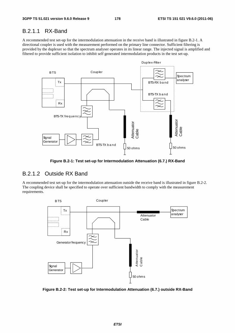
ETSI
ETSI TS 151 021 V9.6.0 (2011-06)1783GPP TS 51.021 version 9.6.0 Release 9
B.2.1.1 RX-Band
A recommended test set-up for the intermodulation attenuation in the receive band is illustrated in figure B.2-1. A directional coupler is used with the measurement performed on the primary line connector. Sufficient filtering is provided by the duplexer so that the spectrum analyser operates in its linear range. The injected signal is amplified and filtered to provide sufficient isolation to inhibit self generated intermodulation products in the test set-up.
Spectrumanalyser
SignalGenerator
BTS Coupler
BTS-TX freq uenc y
BTS-TX b a nd
BTS-RX ba nd
BTS-TX b a nd
Dup lex-Filte r
Tx
Rx
50 ohms 50 ohms
Atte
nuat
orC
able
Atte
nuat
orC
able
Figure B.2-1: Test set-up for Intermodulation Attenuation (6.7.) RX-Band
B.2.1.2 Outside RX Band
A recommended test set-up for the intermodulation attenuation outside the receive band is illustrated in figure B.2-2. The coupling device shall be specified to operate over sufficient bandwidth to comply with the measurement requirements.
Spectrumanalyser
SignalGenerator
B TS Coupler
Generator frequency
Tx
Rx
AttenuatorCable
50 ohms
Att
en
ua
tor
Ca
ble
Figure B.2-2: Test set-up for Intermodulation Attenuation (6.7.) outside RX-Band

ETSI
ETSI TS 151 021 V9.6.0 (2011-06)1793GPP TS 51.021 version 9.6.0 Release 9
B.2.2 Test set-up for Intra BSS Intermodulation Attenuation (6.8.) It is necessary to use different set-ups for the measurement of IM-products in the RX band and in the TX band.
B.2.2.1 RX-Band
A recommended test set-up for the intra base station intermodulation attenuation in the receive band is illustrated in figure B..2-3.
The stop band attenuation of the duplex filter has to be high enough to guarantee that the spectrum analyser is working in its linear range.
SpectrumanalyserBTS
BTS-RX b a nd
BTS-TX b a nd
Dup lex-Filte r
Tx
Rx
50 ohms
AttenuatorCable
Atte
nuat
orC
able
Figure B.2-3: Test set-up for Intra Base station Intermodulation Attenuation (6.8.) RX-Band
B.2.2.2 TX-Band
A recommended test set-up for the intra base station intermodulation attenuation inside the transmit band is illustrated in figure B..2-4. To decrease the dynamic range requirement of the spectrum analyser external filters should be used.
Spectrumanalyser
BTS
Tx
Rx
AttenuatorCable
Figure B.2-4: Test set-up for Intra Base station Intermodulation Attenuation (6.8.) TX-Band

ETSI
ETSI TS 151 021 V9.6.0 (2011-06)1803GPP TS 51.021 version 9.6.0 Release 9
Annex C (informative): Number of samples needed for statistical testing
C.1 GSM 900; Number of samples for testing GSM 900 SDCCH
(FER: 4.25 events/s, frame filling = 4/51)
Prop. cond.
Error rate
Stat. sign.
Indep. samples
Station. proc.
Samples: Time: (s)
static FER=0.10% 30 000 2 - 60 000 14 117.6 TU50 FER=13% 231 2 1 301 1 301 306.1
TU50 (SFH) FER=8% 375 2 1 301 1 301 306.1 RA250 FER=8.0% 375 2 271 750 176.5 HT100 FER=12% 250 2 651 651 153.2
TU3 FER=22% 136 2 21 675 21 675 5 100.0 TU3(SFH) FER=9% 333 2 21 675 21 675 5 100.0
TU50 (SFH) FER=9% 333 2 1 301 1 301 306.1 TI5 FER=13% 231 2 13 005 13 005 3 060.0
GSM 900 RACH
(FER: 217 events/s, frame filling = 1)
Prop. cond.
Error rate
Stat. sign.
Indep. samples
Station. proc.
Samples: Time: (s)
static FER=0.50% 6 000 2 - 12 000 55.3 TU50 FER=13% 231 2 5 208 5 208 24.0
RA250 FER=12% 250 2 1 085 1 085 5.0 HT100 FER=13% 231 2 2 604 2 604 12.0 TU3 FER=15% 200 2 86 800 86 800 400.0
TU3(SFH) FER=15% 200 2 86 800 86 800 400.0 TU50 FER=16% 188 2 5 208 5 208 24.0
RA250 FER=13% 231 2 1 085 1 085 5.0 TU50(SFH) FER=13% 231 2 5 208 5 208 24.0
TI5 FER=13% 231 2 52 080 52 080 240.0 TU50(SFH) FER=16% 188 2 5 208 5 208 24.0
TI5 FER=16% 188 2 52 080 52 080 240.0
GSM 900 SACCH/T
(FER: 2.1 events/s, frame filling = 1/26)
Prop. cond.
Error rate
Stat. sign.
Indep. samples
Station. proc.
Samples: Time: (s)
static FER=0.10% 30 000 2 - 60 000 28 571.4 TU50 FER=13% 231 2 1 311 1 311 624.3
TU50(SFH) FER=8% 375 2 1 311 1311 624.3 RA250 FER=8.0% 375 2 273 750 357.1 HT100 FER=12% 250 2 656 656 312.4 TU3 FER=22% 136 2 21 840 21 840 10 400.0
TU3(SFH) FER=9% 333 2 21 840 21 840 10 400.0 TU50(SFH) FER=9% 333 2 1 311 1 311 624.3
TI5 FER=13% 231 2 13 104 13 104 6 240.0

ETSI
ETSI TS 151 021 V9.6.0 (2011-06)1813GPP TS 51.021 version 9.6.0 Release 9
GSM 900 SACCH/C
(FER: 2.13 events/s, frame filling = 4/102)
Prop. cond.
Error rate
Stat. sign.
Indep. samples
Station. proc.
Samples: Time: (s)
static FER=0.10% 30 000 2 - 60 000 28 169.0 TU50 FER=13% 231 2 1 304 1 304 612.2
TU50(SFH) FER=8% 375 2 1 304 1 304 612.2 RA250 FER=8.0% 375 2 272 750 352.1 HT100 FER=12% 250 2 652 652 306.1 TU3 FER=22% 136 2 21 726 21 726 10 200.0
TU3(SFH) FER=9% 333 2 21 726 21 726 10 200.0 TU50(SFH) FER=9% 333 2 1 304 1 304 612.2
TI5 FER=13% 231 2 26 071 26 071 12 240
GSM 900 FACCH/F
(FER: 50 events/s, frame filling = 24/26)
Prop. cond.
Error rate
Stat. sign.
Indep. samples
Station. proc.
Samples: Time: (s)
static FER=0.10% 30 000 4 - 120 000 2 400.0 TU50 FER=8% 375 4 1 300 1 500 30.0
TU50(SFH) FER=3.8% 789 4 1 300 3 156 63.1 RA250 FER=3.4% 882 4 271 3 528 70.6 HT100 FER=6.3% 476 4 650 1 904 38.1 TU3 FER=22% 136 4 21 667 21 667 433.3
TU3(SFH) FER=3.4% 882 4 21 667 21 667 433.3 TU50 FER=9.5% 316 4 1 300 1 300 26.0
TU50(SFH) FER=3.4% 882 4 1 300 1 300 70.6 RA250 FER=3.5% 857 4 271 3 428 68.6
TI5 FER=8.0% 375 4 13 000 13 000 260.0 TI5 FER=9.5% 316 4 13 000 13 000 260.0
TU50 FER=17.1% 176 4 1300 1300 26.0 TI5 FER=17.1% 176 4 13 000 13 000 260.0
GSM 900 FACCH/H
(FER: 25 events/s, frame filling = 12/26)
Prop. cond.
Error rate
Stat. sign.
Indep. samples
Station. proc.
Samples: Time: (s)
static FER=0.10% 30 000 4 - 120 000 4 800.0 TU50 FER=6.9% 435 4 1 300 1 740 69.6
RA250 FER=5.7% 526 4 271 2 104 84.2 HT100 FER=10% 300 4 650 1 200 48.0 TU3 FER=22% 136 4 21 667 21 667 866.7
TU3(SFH) FER=6.7% 448 4 21 667 21 667 866.7 TU50 FER=6.7% 448 4 1 300 1 792 71.7
TU50(SFH) FER=6.9% 435 4 1 300 1 740 69.6 TI5 FER=6.9% 435 4 13 000 13 000 520.0
TU50(SFH) FER=6.7% 448 4 1 300 1 792 71.7 TI5 FER=6.7% 448 4 13 000 13 000 520.0
GSM 900 TCH/F9.6
(BER: 12000 events/s, frame filling = 24/26)

ETSI
ETSI TS 151 021 V9.6.0 (2011-06)1823GPP TS 51.021 version 9.6.0 Release 9
Prop. cond.
Error rate
Stat. sign.
Indep. samples
Station. proc.
Samples: Time: (s)
static BER=1.0E-5 3000 000 10 - 30000 000 2 500.0 TU50 BER=0.50% 6 000 10 312 000 312 000 26.0
TU50(SFH) BER=0.4% 7 500 10 312 000 312 000 26.0 RA250 BER=0.10% 30 000 10 65 000 300 000 25.0 HT100 BER=0.70% 4 286 10 156 000 156 000 13.0
TU3 BER=8.0% 375 10 5200 000 5200 000 433.3 TU3(SFH) BER=0.30% 10 000 10 5200 000 5200 000 433.3
TU50 BER=0.80% 3750 10 312 000 312 000 26.0 TU50(SFH) BER=0.3% 10 000 10 312 000 312 000 26.0
RA250 BER=0.20% 15 000 10 65 000 150 000 12.5 TI5 BER=0.5% 6 000 10 3 120 000 3 120 000 260.0 TI5 BER=0.8% 3 750 10 3 120 000 3 120 000 260.0
GSM 900 TCH/H4.8
(BER: 6000 events/s, frame filling = 12/26)
Prop. cond.
Error rate
Stat. sign.
Indep. samples
Station. proc.
Samples: Time: (s)
static BER=1.0E-5 3000 000 10 - 30000 000 5 000.0 TU50 BER=0.50% 6 000 10 312 000 312 000 52.0
TU50(SFH) BER=0.4% 7500 10 312 000 312 000 52.0 RA250 BER=0.10% 30 000 10 65 000 300 000 50.0 HT100 BER=0.70% 4 286 10 156 000 156 000 26.0 TU3 BER=8.0% 375 10 5200 000 5200 000 866.7
TU3(SFH) BER=0.30% 10 000 10 5200 000 5200 000 866.7 TU50 BER=0.8% 3 750 10 312 000 312 000 52.0
TU50(SFH) BER=0.3% 10 000 10 312 000 312 000 52.0 RA250 BER=0.20% 15 000 10 65 000 150 000 25.0
TI5 BER=0.5% 6 000 10 3 120 000 3 120 000 520.0 TI5 BER=0.8% 3 750 10 3 120 000 3 120 000 520.0
GSM 900 TCH/F4.8
(BER: 6000 events/s, frame filling = 24/26)
Prop. cond.
Error rate
Stat. sign.
Indep. samples
Station. proc.
Samples: Time: (s)
TU50 BER=1.0E-4 300 000 10 156 000 3000 000 500.0 RA250 BER=1.0E-4 300 000 10 32 500 3000 000 500.0 HT100 BER=1.0E-4 300 000 10 78 000 3000 000 500.0 TU3 BER=3.0% 1 000 10 2600 000 2600 000 433.3
TU3(SFH) BER=1.0E-4 300 000 10 2600 000 3000 000 500.0 TU50(SFH) BER=1.0E-4 300 000 10 1 560 000 3 000 000 260.0
TI5 BER=1.0E-4 300 000 10 1 560 000 3 000 000 260.0

ETSI
ETSI TS 151 021 V9.6.0 (2011-06)1833GPP TS 51.021 version 9.6.0 Release 9
GSM 900 TCH/F2.4
(BER: 3600 events/s, frame filling = 24/26)
Prop. cond.
Error rate
Stat. sign.
Indep. samples
Station. proc.
Samples: Time: (s)
TU50 BER=2.0E-04 1500 00 10 93 600 15000 00 416.7 RA250 BER=1.0E-5 3 000 000 10 3 900 30 000 000 8 333.3 HT100 BER=1.0E-5 3 000 000 10 46 800 30 000 000 8 333.3 TU3 BER=3.0% 1 000 10 1 560 000 1 560 000 433.3
TU3(SFH) BER=1.0E-5 3 000 000 10 1 560 000 30 000 000 8 333.3 TU50 BER=3.0E-5 1 000 000 10 93 600 10 000 000 2 777.8
TU50(SFH) BER=1E-05 3 000 000 10 93 600 30 000 000 8 333.3 TI5 BER=2.0E-4 150 000 10 936 000 1 500 000 416.7
TU50 BER=1.0E-4 300 000 10 93 600 3 000 000 833.3 TI5 BER=1.0E-4 300 000 10 936 000 3 000 000 833.3
GSM 900 TCH/H2.4
(BER: 3600 events/s, frame filling = 12/26)
Prop. cond.
Error rate
Stat. sign.
Indep. samples
Station. proc.
Samples: Time: (s)
TU50 BER=1.0E-4 300 000 10 187 200 3 000 000 833.3 RA250 BER=1.0E-4 300 000 10 39 000 3 000 000 833.3 HT100 BER=1.0E-4 300 000 10 93 600 3 000 000 833.3 TU3 BER=4.0% 750 10 3 120 000 3 120 000 866.7
TU3(SFH) BER=1.0E-4 300 000 10 3 120 000 3 120 000 866.7 TU50 BER=2.0E-4 150 000 10 187 200 1 500 000 416.7
TU50(SFH) BER=1.0E-04 300 000 10 187 200 3 000 000 833.3 TI5 BER=1.0E-4 300 000 10 1 872 000 3 000 000 833.3 TI5 BER=2.0E-4 150 000 10 1 872 000 1 872 000 520.0

ETSI
ETSI TS 151 021 V9.6.0 (2011-06)1843GPP TS 51.021 version 9.6.0 Release 9
GSM 900 TCH/FS
(FER: 50 events/s, RBER class Ib: 6600 events/s, RBER class II: 3900 events/s, frame filling = 24/26)
Prop. cond.
Error rate
Stat. sign.
Indep. samples
Station. proc.
Samples: Time: (s)
static FER=0.10% 30 000 4 - 120 000 2 400.0 Ib RBER=0.40% 7 500 10 - 75 000 11.4 II RBER=2.0% 1 500 10 - 15 000 3.8
TU50 FER=6.0% 500 4 1 300 2 000 40.0 Ib RBER=0.40% 7 500 10 171 600 171 600 26.0 II RBER=8.0% 375 10 101 400 101 400 26.0
TU50(SFH) FER=3% 1 000 4 1 300 4 000 80.0 Ib RBER=0.3% 10 000 10 171 600 171 600 26.0 II RBER=8% 375 10 101 400 101 400 26.0
RA250 FER=2.0% 1 500 4 271 6 000 120.0 Ib RBER=0.20% 15 000 10 35 750 150 000 22.7 II RBER=7.0% 429 10 21 125 21 125 5.4
HT100 FER=7.0% 429 4 650 1 716 34.3 Ib RBER=0.50% 6 000 10 85 800 85 800 13.0 II RBER=9.0% 333 10 50 700 50 700 13.0
TU3 FER=21% 143 4 21 667 21 667 433.3 Ib RBER=2.0% 1 500 10 2860 000 2 860 000 433.3 II RBER=4.0% 750 10 1690 000 1 690 000 433.3
TU3(SFH) FER=3.0% 1 000 4 21 667 21 667 433.3 Ib RBER=0.20% 15 000 10 2860 000 2 860 000 433.3 II RBER=8.0% 375 10 1690 000 1 690 000 433.3
TU50(SFH) FER=3% 1 000 4 1 300 4 000 80.0 Ib RBER=0.2% 15 000 10 171 600 171 600 26.0 II RBER=8% 375 10 101 400 101 400 26.0
RA250 FER=3.0% 1 000 4 271 4 000 80.0 Ib RBER=0.20% 15 000 10 35 750 150 000 22.7 II RBER=8.0% 375 10 21 125 21 125 5.4
static II RBER=1.0E-4 300 000 10 - 3 000 000 769.2 EQU50 II RBER=3.0% 1 000 10 101 400 101 400 26.0
static FER=5% 600 4 - 2400 48.0 TI5 FER=6% 500 4 13 000 13 000 260.0 Ib RBER=0.4% 7500 10 1 716 000 1 716 000 260.0 II RBER=8.0% 375 10 1 014 000 1 014 000 260.0
TU50 FER=10.2% 294 4 1 300 1 300 26.0 Ib RBER=0.72% 4167 10 171 600 171 600 26.0 II RBER=8.8% 341 10 101 400 101 400 26.0
TI5 FER=10.2% 294 4 13 000 1 300 26.0 Ib RBER=0.72% 4167 10 1 716 000 1 716 000 260.0 II RBER=8.8% 341 10 1 014 000 1 014 000 260.0
GSM 900 TCH/F14.4
(BER: 14500 events/s, frame filling = 24/26)
Prop. cond.
Error rate
Stat. Sign.
Indep. samples
Station. proc.
Samples: Time: (s)
static BER=1.0E-5 3 000 000 10 - 30 000 000 2 069.0 TU50 BER=2.5% 1 200 10 377 000 377 000 26.0
TU50(SFH) BER=2.0% 1 500 10 377 000 377 000 26.0 RA250 BER=2.0% 1 500 10 78 542 78 542 5.4 HT100 BER=5.0% 600 10 188 500 188 500 13.0 TU3 BER=10.0% 300 10 6 283 333 6 283 333 433.3
TU3(SFH) BER=3.0% 1000 10 6 283 333 6 283 333 433.3 TU50(SFH) BER=3.0% 1 000 10 377 000 377 000 26.0

ETSI
ETSI TS 151 021 V9.6.0 (2011-06)1853GPP TS 51.021 version 9.6.0 Release 9
RA250 BER=3.0% 1 000 10 78 542 78 542 5.4 TU50 BER=4.5% 667 10 377 000 377 000 26.0 TI5 BER=2.5% 1 200 10 3 770 000 3 770 000 260.0 TI5 BER=4.5% 667 10 3 770 000 3 770 000 260.0
GSM 900 TCH/HS
(FER: 50 events/s, RBER class Ib: 3650 events/s, RBER class II: 850 events/s, frame filling = 12/26)
Prop. cond.
Error rate
Stat. sign.
Indep. samples
Station. proc.
Samples: Time: (s)
static (FER) 0.025% 120 000 4 - 480 000 9 600.0 Ib 0.001% 3 000 000 10 - 30 000 000 8 219.2 II 0.720% 4 167 10 - 41 667 49.0
TU50 (FER) 4.10% 732 4 2 600 2 927 58.5 Ib 0.36% 8 333 10 189 800 189 800 52.0 II 6.90% 435 10 44 200 44 200 52.0
RA250 (FER) 4.10% 732 4 542 2 927 58.5 Ib 0.28% 10 714 10 39 542 107 143 29.4 II 6.80% 441 10 9 208 9 208 10.8
HT100 (FER) 4.50% 667 4 1 300 2 667 53.3 Ib 0.56% 5 357 10 94 900 94 900 26.0 II 7.60% 395 10 22 100 22 100 26.0
TU3 (FER) 19.10% 157 4 43 333 43 333 866.7 Ib 0.52% 5 769 10 3 163 333 3 163 333 866.7 II 2.80% 1 071 10 736 667 736 667 866.7
TU50 (FER) 5.00% 600 4 2 600 2 600 52.0 Ib 0.29% 10 345 10 189 800 189 800 52.0 II 7.10% 423 10 44 200 44 200 52.0
RA250 (FER) 4.70% 638 4 542 2 553 51.1 Ib 0.21% 14 286 10 39 542 142 857 39.1 II 7.00% 429 10 9 208 9 208 10.8
TU50 (SFH) FER 4.10% 732 4 2 600 2 927 58.5 Ib 0.36% 8 333 10 189 800 189 800 52.0 II 6.90% 435 10 44 200 44 200 52.0
TI5 (FER) 4.1% 732 4 26 000 26 000 520.0 Ib 0.36% 8 333 10 1 898 000 1 898 000 520.0 II 6.9% 435 10 442 000 442 000 520.0
TU50 (SFH) FER 5.0% 600 4 2 600 2 600 52.0 Ib 0.29% 10 345 10 189 800 189 800 52.0 II 7.1% 423 10 44 200 44 200 52.0
TI5 (FER) 5.0% 600 4 26 000 26 000 520.0 Ib 0.29% 10 345 10 1 898 000 1 898 000 520.0 II 7.1% 423 10 442 000 442 000 520.0
To reduce the testing time on static FER and RBER class 1b the factor k = Pb/Ps may be increased from k = 2 to
k > 2 thus resulting in reasonable reductions of the test times, see table below. If this test fails, the test may be repeated with the number of samples given in the table above.
Prop. cond.
k = Pb/Ps Stat. sign.
Indep. samples
Samples: Time: (s)
Probability of no error (1 - p)
static (FER) 2.5 60 000 4 240 000 4800 (1h20') 6.8 %
Ib 2.5 1 500 000 10 15 000 000 4110 (1h08') 6.8 %
static (FER) 3.0 40 000 4 160 000 2880 (48') 15.8 % Ib 3.0 1 000 000 10 10 000 000 2466 (41') 15.8 %

ETSI
ETSI TS 151 021 V9.6.0 (2011-06)1863GPP TS 51.021 version 9.6.0 Release 9
GSM 900 TCH/EFS
(FER: 50 events/s, RBER class Ib: 6600 events/s, RBER class II: 3900 events/s, frame filling = 24/26)
Prop. cond.
Error rate
Stat. sign.
Indep. samples
Station. proc.
Samples: Time: (s)
static FER=0.10% 30 000 4 - 120 000 2 400.0 Ib RBER=0.10% 30 000 10 - 300 000 45.5 II RBER=2.0% 1 500 10 - 15 000 3.8
TU50 FER=8.0% 375 4 1 300 3 000 60.0 Ib RBER=0.21% 14 286 10 171 600 171 600 26.0 II RBER=7.0% 429 10 101 400 101 400 26.0
TU50(SFH) FER=3.0% 1 000 4 1 300 4 000 80.0 Ib RBER=0.11% 27 273 10 171 600 272 730 41.3 II RBER=8.0% 375 10 101 400 101 400 26.0
RA250 FER=3.0% 1 000 4 271 4 000 80.0 Ib RBER=0.10% 30 000 10 35 750 300 000 45.5 II RBER=7.0% 429 10 21 125 21 125 5.4
HT100 FER=7.0% 429 4 650 1 716 34.3 Ib RBER=0.20% 15 000 10 85 800 150 000 22.7 II RBER=9.0% 333 10 50 700 50 700 13.0
TU3 FER=23% 130 4 21 667 21 667 433.3 Ib RBER=0.20% 15 000 10 2860 000 2860 000 433.3 II RBER=3.0% 1 000 10 1690 000 1690 000 433.3
TU3(SFH) FER=3.0% 1 000 4 21 667 21 667 433.3 Ib RBER=0.1% 30 000 10 2860 000 2860 000 433.3 II RBER=8.0% 375 10 1690 000 1690 000 433.3
TU50 FER=9.0% 333 4 1 300 1 332 26.6 Ib RBER=0.2% 15 000 10 171 600 171 600 26.0 II RBER=7.0% 429 10 101 400 101 400 26.0
TU50(SFH) FER=3.0% 1 000 4 1 300 4 000 80.0 Ib RBER=0.1% 30 000 10 171 600 300 000 45.5 II RBER=8.0% 375 10 101 400 101 400 26.0
RA250 FER=4.0% 750 4 271 3 000 60.0 Ib RBER=0.13% 23 077 10 35 750 230 770 35.0 II RBER=8.0% 375 10 21 125 21 125 5.4
TI5 FER=8.0% 375 4 13 000 13 000 260.0 Ib RBER=0.21% 14 286 10 1 716 000 1 716 000 260.0 II RBER=7.0% 429 10 1 014 000 1 014 000 260.0
TI5 FER=9.0% 333 4 13 000 13 000 260.0 Ib RBER=0.2% 15 000 10 1 716 000 1 716 000 260.0 II RBER=7.0% 429 10 1 014 000 1 014 000 260.0
ETSI
ETSI TS 151 021 V9.6.0 (2011-06)1873GPP TS 51.021 version 9.6.0 Release 9
GSM 900 TCH/AFS12.2
(FER: 50 events/s, RBER class Ib: 12200 events/s, frame filling = 24/26)
Prop. cond.
Error rate
Stat. sign.
Indep. samples
Station. proc.
Samples: Time: (s)
Static (Ib) RBER = 0,001 % 3000000 10 - 30000000 2459 TU50 (no SFH) FER = 4,9 % 612,2 4 1300 2449 49
Ib RBER = 1,5 % 2000 10 317200 317200 26 TU50 (ideal SFH) FER = 2,4 % 1250 4 1300 5000 100
Ib RBER = 1,5 % 2000 10 317200 317200 26 RA250 (no SFH) FER = 1,4 % 2142,9 4 270,8 8571,4 171,4
Ib RBER = 1,2 % 2500 10 66083,3 66083,3 5,4 HT100 (no SFH) FER = 4,5 % 666,7 4 650 2666,7 53,3
Ib RBER = 2,1 % 1428,6 10 158600 158600 13 TI5 (no SFH) FER = 4,9 % 612,2 4 13000 13000 260
Ib RBER = 1,5 % 2000 10 3172000 3172000 260 TU3 (no SFH) FER = 22 % 136,4 4 21666,7 21666,7 433,3
Ib RBER = 0,9 % 3333,3 10 5286666,7 5286666,7 433,3 TU50 (no SFH) FER = 6 % 500 4 1300 2000 40
Ib RBER = 1,7 % 1764,7 10 317200 317200 26 TU50 (ideal SFH) FER = 3,5 % 857,1 4 1300 3428,6 68,6
Ib RBER = 1,7 % 1764,7 10 317200 317200 26 RA250 (no SFH) FER = 2,5 % 1200 4 270,8 4800 96
Ib RBER = 1,5 % 2000 10 66083,3 66083,3 5,4 TI5 (no SFH) FER = 6 % 500 4 13000 13000 260
Ib RBER = 1,7 % 1764,7 10 3172000 3172000 260
GSM 900 TCH/AFS10.2
(FER: 50 events/s, RBER class Ib: 10200 events/s, frame filling = 24/26)
Prop. cond.
Error rate
Stat. sign.
Indep. samples
Station. proc.
Samples: Time: (s)
Static (Ib) RBER = 0,001 % 3000000 10 - 30000000 2941,2 TU50 (no SFH) FER = 2,1 % 1428,6 4 1300 5714,3 114,3
Ib RBER = 0,23 % 13043,5 10 265200 265200 26 TU50 (ideal SFH) FER = 0,85 % 3529,4 4 1300 14117,6 282,4
Ib RBER = 0,15 % 20000 10 265200 265200 26 RA250 (no SFH) FER = 0,45 % 6666,7 4 270,8 26666,7 533,3
Ib RBER = 0,092 % 32608,7 10 55250 326087 32 HT100 (no SFH) FER = 1,6 % 1875 4 650 7500 150
Ib RBER = 0,26 % 11538,5 10 132600 132600 13 TI5 (no SFH) FER = 2,1 % 1428,6 4 13000 13000 260
Ib RBER = 0,23 % 13043,5 10 2652000 2652000 260 TU3 (no SFH) FER = 18 % 166,7 4 21666,7 21666,7 433,3
Ib RBER = 0,53 % 5660,4 10 4420000 4420000 433,3 TU50 (no SFH) FER = 2,7 % 1111,1 4 1300 4444,4 88,9
Ib RBER = 0,3 % 10000 10 265200 265200 26 TU50 (ideal SFH) FER = 1,4 % 2142,9 4 1300 8571,4 171,4
Ib RBER = 0,21 % 14285,7 10 265200 265200 26 RA250 (no SFH) FER = 0,92 % 3260,9 4 270,8 13043,5 260,9
Ib RBER = 0,16 % 18750 10 55250 187500 18,4 TI5 (no SFH) FER = 2,7 % 1111,1 4 13000 13000 260
Ib RBER = 0,3 % 10000 10 2652000 2652000 260

ETSI
ETSI TS 151 021 V9.6.0 (2011-06)1883GPP TS 51.021 version 9.6.0 Release 9
GSM 900 TCH/AFS7.95
(FER: 50 events/s, RBER class Ib: 7950 events/s, frame filling = 24/26)
Prop. cond.
Error rate
Stat. sign.
Indep. samples
Station. proc.
Samples: Time: (s)
TU50 (no SFH) FER = 0,36 % 8333,3 4 1300 33333,3 666,7 Ib RBER = 0,11 % 27272,7 10 206700 272727,3 34,3
TU50 (ideal SFH) FER = 0,045 % 66666,7 4 1300 266666,7 5333,3 Ib RBER = 0,032 % 93750 10 206700 937500 117,9
RA250 (no SFH) FER = 0,024 % 125000 4 270,8 500000 10000 Ib RBER = 0,02 % 150000 10 43062,5 1500000 188,7
HT100 (no SFH) FER = 0,096 % 31250 4 650 125000 2500 Ib RBER = 0,06 % 50000 10 103350 500000 62,9
TI5 (no SFH) FER = 0,36 % 8333,3 4 13000 33333,3 666,7 Ib RBER = 0,11 % 27272,7 10 2067000 2067000 260
TU3 (no SFH) FER = 13 % 230,8 4 21666,7 21666,7 433,3 Ib RBER = 0,66 % 4545,5 10 3445000 3445000 433,3
TU50 (no SFH) FER = 0,51 % 5882,4 4 1300 23529,4 470,6 Ib RBER = 0,15 % 20000 10 206700 206700 26
TU50 (ideal SFH) FER = 0,12 % 25000 4 1300 100000 2000 Ib RBER = 0,065 % 46153,8 10 206700 461538,5 58,1
RA250 (no SFH) FER = 0,073 % 41095,9 4 270,8 164383,6 3287,7 Ib RBER = 0,044 % 68181,8 10 43062,5 681818,2 85,8
TI5 (no SFH) FER = 0,51 % 5882,4 4 13000 23529,4 470,6 Ib RBER = 0,15 % 20000 10 2067000 2067000 260
TU3 (no SFH) FER = 26 % 115,4 4 21666,7 21666,7 433,3 Ib RBER = 1,2 % 2500 10 3445000 3445000 433,3
TU50 (no SFH) FER = 5,3 % 566 4 1300 2264,2 45,3 Ib RBER = 1 % 3000 10 206700 206700 26
TU50 (ideal SFH) FER = 2,7 % 1111,1 4 1300 4444,4 88,9 Ib RBER = 0,78 % 3846,2 10 206700 206700 26
RA250 (no SFH) FER = 1,8 % 1666,7 4 270,8 6666,7 133,3 Ib RBER = 0,6 % 5000 10 43062,5 50000 6,3
TI5 (no SFH) FER = 5,3 % 566 4 13000 13000 260 Ib RBER = 1 % 3000 10 2067000 2067000 260

ETSI
ETSI TS 151 021 V9.6.0 (2011-06)1893GPP TS 51.021 version 9.6.0 Release 9
GSM 900 TCH/AFS7.4
(FER: 50 events/s, RBER class Ib: 7400 events/s, frame filling = 24/26)
Prop. cond.
Error rate
Stat. sign.
Indep. samples
Station. proc.
Samples: Time: (s)
TU50 (no SFH) FER = 0,41 % 7317,1 4 1300 29268,3 585,4 Ib RBER = 0,054 % 55555,6 10 192400 555555,6 75,1
TU50 (ideal SFH) FER = 0,069 % 43478,3 4 1300 173913 3478,3 Ib RBER = 0,016 % 187500 10 192400 1875000 253,4
RA250 (no SFH) FER = 0,028 % 107142,9 4 270,8 428571,4 8571,4 Ib RBER = 0,009 % 333333,3 10 40083,3 3333333,3 450,5
HT100 (no SFH) FER = 0,13 % 23076,9 4 650 92307,7 1846,2 Ib RBER = 0,033 % 90909,1 10 96200 909090,9 122,9
TI5 (no SFH) FER = 0,41 % 7317,1 4 13000 29268,3 585,4 Ib RBER = 0,054 % 55555,6 10 1924000 1924000 260
TU3 (no SFH) FER = 14 % 214,3 4 21666,7 21666,7 433,3 Ib RBER = 0,43 % 6976,7 10 3206666,7 3206666,7 433,3
TU50 (no SFH) FER = 0,56 % 5357,1 4 1300 21428,6 428,6 Ib RBER = 0,072 % 41666,7 10 192400 416666,7 56,3
TU50 (ideal SFH) FER = 0,16 % 18750 4 1300 75000 1500 Ib RBER = 0,032 % 93750 10 192400 937500 126,7
RA250 (no SFH) FER = 0,09 % 33333,3 4 270,8 133333,3 2666,7 Ib RBER = 0,018 % 166666,7 10 40083,3 1666666,7 225,2
TI5 (no SFH) FER = 0,56 % 5357,1 4 13000 21428,6 428,6 Ib RBER = 0,072 % 41666,7 10 1924000 1924000 260
TU3 (no SFH) FER = 26 % 115,4 4 21666,7 21666,7 433,3 Ib RBER = 0,79 % 3797,5 10 3206666,7 3206666,7 433,3
TU50 (no SFH) FER = 5,4 % 555,6 4 1300 2222,2 44,4 Ib RBER = 0,52 % 5769,2 10 192400 192400 26
TU50 (ideal SFH) FER = 3,1 % 967,7 4 1300 3871 77,4 Ib RBER = 0,38 % 7894,7 10 192400 192400 26
RA250 (no SFH) FER = 2 % 1500 4 270,8 6000 120 Ib RBER = 0,28 % 10714,3 10 40083,3 107142,9 14,5
TI5 (no SFH) FER = 5,4 % 555,6 4 13000 13000 260 Ib RBER = 0,52 % 5769,2 10 1924000 1924000 260

ETSI
ETSI TS 151 021 V9.6.0 (2011-06)1903GPP TS 51.021 version 9.6.0 Release 9
GSM 900 TCH/AFS6.7
(FER: 50 events/s, RBER class Ib: 6700 events/s, frame filling = 24/26)
Prop. cond.
Error rate
Stat. sign.
Indep. samples
Station. proc.
Samples: Time: (s)
TU50 (no SFH) FER = 0,16 % 18750 4 1300 75000 1500 Ib RBER = 0,082 % 36585,4 10 174200 365853,7 54,6
TU50 (ideal SFH) FER = 0,017 % 176470,6 4 1300 705882,4 14117,6 Ib RBER = 0,022 % 136363,6 10 174200 1363636,4 203,5
RA250 (no SFH) FER = 0,01 % 300000 4 270,8 1200000 24000 Ib RBER = 0,013 % 230769,2 10 36291,7 2307692,3 344,4
HT100 (no SFH) FER = 0,026 % 115384,6 4 650 461538,5 9230,8 Ib RBER = 0,044 % 68181,8 10 87100 681818,2 101,8
TI5 (no SFH) FER = 0,16 % 18750 4 13000 75000 1500 Ib RBER = 0,082 % 36585,4 10 1742000 1742000 260
TU3 (no SFH) FER = 11 % 272,7 4 21666,7 21666,7 433,3 Ib RBER = 0,75 % 4000 10 2903333,3 2903333,3 433,3
TU50 (no SFH) FER = 0,21 % 14285,7 4 1300 57142,9 1142,9 Ib RBER = 0,11 % 27272,7 10 174200 272727,3 40,7
TU50 (ideal SFH) FER = 0,041 % 73170,7 4 1300 292682,9 5853,7 Ib RBER = 0,042 % 71428,6 10 174200 714285,7 106,6
RA250 (no SFH) FER = 0,021 % 142857,1 4 270,8 571428,6 11428,6 Ib RBER = 0,028 % 107142,9 10 36291,7 1071428,6 159,9
TI5 (no SFH) FER = 0,21 % 14285,7 4 13000 57142,9 1142,9 Ib RBER = 0,11 % 27272,7 10 1742000 1742000 260
TU3 (no SFH) FER = 23 % 130,4 4 21666,7 21666,7 433,3 Ib RBER = 1,4 % 2142,9 10 2903333,3 2903333,3 433,3
TU50 (no SFH) FER = 2,9 % 1034,5 4 1300 4137,9 82,8 Ib RBER = 0,86 % 3488,4 10 174200 174200 26
TU50 (ideal SFH) FER = 1,2 % 2500 4 1300 10000 200 Ib RBER = 0,6 % 5000 10 174200 174200 26
RA250 (no SFH) FER = 0,75 % 4000 4 270,8 16000 320 Ib RBER = 0,44 % 6818,2 10 36291,7 68181,8 10,2
TI5 (no SFH) FER = 2,9 % 1034,5 4 13000 13000 260 Ib RBER = 0,86 % 3488,4 10 1742000 1742000 260

ETSI
ETSI TS 151 021 V9.6.0 (2011-06)1913GPP TS 51.021 version 9.6.0 Release 9
GSM 900 TCH/AFS5.9
(FER: 50 events/s, RBER class Ib: 5900 events/s, frame filling = 24/26)
Prop. cond.
Error rate
Stat. sign.
Indep. samples
Station. proc.
Samples: Time: (s)
TU50 (no SFH) FER = 0,094 % 31914,9 4 1300 127659,6 2553,2 Ib RBER = 0,014 % 214285,7 10 153400 2142857,1 363,2
TU50 (ideal SFH) FER = 0,01 % 300000 4 1300 1200000 24000 Ib RBER = 0,001 % 3000000 10 153400 30000000 5084,7
RA250 (no SFH) FER = 0,01 % 300000 4 270,8 1200000 24000 Ib RBER = 0,001 % 3000000 10 31958,3 30000000 5084,7
HT100 (no SFH) FER = 0,011 % 272727,3 4 650 1090909,1 21818,2 Ib RBER = 0,003 % 1000000 10 76700 10000000 1694,9
TI5 (no SFH) FER = 0,094 % 31914,9 4 13000 127659,6 2553,2 Ib RBER = 0,014 % 214285,7 10 1534000 2142857,1 363,2
TU3 (no SFH) FER = 10 % 300 4 21666,7 21666,7 433,3 Ib RBER = 0,38 % 7894,7 10 2556666,7 2556666,7 433,3
TU50 (no SFH) FER = 0,12 % 25000 4 1300 100000 2000 Ib RBER = 0,022 % 136363,6 10 153400 1363636,4 231,1
TU50 (ideal SFH) FER = 0,018 % 166666,7 4 1300 666666,7 13333,3 Ib RBER = 0,005 % 600000 10 153400 6000000 1016,9
RA250 (no SFH) FER = 0,01 % 300000 4 270,8 1200000 24000 Ib RBER = 0,003 % 1000000 10 31958,3 10000000 1694,9
TI5 (no SFH) FER = 0,12 % 25000 4 13000 100000 2000 Ib RBER = 0,022 % 136363,6 10 1534000 1534000 260
TU3 (no SFH) FER = 21 % 142,9 4 21666,7 21666,7 433,3 Ib RBER = 0,74 % 4054,1 10 2556666,7 2556666,7 433,3
TU50 (no SFH) FER = 2 % 1500 4 1300 6000 120 Ib RBER = 0,23 % 13043,5 10 153400 153400 26
TU50 (ideal SFH) FER = 0,7 % 4285,7 4 1300 17142,9 342,9 Ib RBER = 0,12 % 25000 10 153400 250000 42,4
RA250 (no SFH) FER = 0,4 % 7500 4 270,8 30000 600 Ib RBER = 0,079 % 37974,7 10 31958,3 379746,8 64,4
TI5 (no SFH) FER = 2 % 1500 4 13000 13000 260 Ib RBER = 0,23 % 13043,5 10 1534000 1534000 260

ETSI
ETSI TS 151 021 V9.6.0 (2011-06)1923GPP TS 51.021 version 9.6.0 Release 9
GSM 900 TCH/AFS5.15
(FER: 50 events/s, RBER class Ib: 5150 events/s, frame filling = 24/26)
Prop. cond.
Error rate
Stat. sign.
Indep. samples
Station. proc.
Samples: Time: (s)
TU50 (no SFH) FER = 0,07 % 42857,1 4 1300 171428,6 3428,6 Ib RBER = 0,014 % 214285,7 10 133900 2142857,1 416,1
TU50 (ideal SFH) FER = 0,01 % 300000 4 1300 1200000 24000 Ib RBER = 0,001 % 3000000 10 133900 30000000 5825,2
RA250 (no SFH) FER = 0,01 % 300000 4 270,8 1200000 24000 Ib RBER = 0,001 % 3000000 10 27895,8 30000000 5825,2
HT100 (no SFH) FER = 0,01 % 300000 4 650 1200000 24000 Ib RBER = 0,002 % 1500000 10 66950 15000000 2912,6
TI5 (no SFH) FER = 0,07 % 42857,1 4 13000 171428,6 3428,6 Ib RBER = 0,014 % 214285,7 10 1339000 2142857,1 416,1
TU3 (no SFH) FER = 9,2 % 326,1 4 21666,7 21666,7 433,3 Ib RBER = 0,44 % 6818,2 10 2231666,7 2231666,7 433,3
TU50 (no SFH) FER = 0,081 % 37037 4 1300 148148,1 2963 Ib RBER = 0,019 % 157894,7 10 133900 1578947,4 306,6
TU50 (ideal SFH) FER = 0,011 % 272727,3 4 1300 1090909,1 21818,2 Ib RBER = 0,003 % 1000000 10 133900 10000000 1941,7
RA250 (no SFH) FER = 0,01 % 300000 4 270,8 1200000 24000 Ib RBER = 0,002 % 1500000 10 27895,8 15000000 2912,6
TI5 (no SFH) FER = 0,081 % 37037 4 13000 148148,1 2963 Ib RBER = 0,019 % 157894,7 10 1339000 1578947,4 306,6
TU3 (no SFH) FER = 19 % 157,9 4 21666,7 21666,7 433,3 Ib RBER = 0,85 % 3529,4 10 2231666,7 2231666,7 433,3
TU50 (no SFH) FER = 1,4 % 2142,9 4 1300 8571,4 171,4 Ib RBER = 0,22 % 13636,4 10 133900 136363,6 26,5
TU50 (ideal SFH) FER = 0,47 % 6383 4 1300 25531,9 510,6 Ib RBER = 0,11 % 27272,7 10 133900 272727,3 53
RA250 (no SFH) FER = 0,25 % 12000 4 270,8 48000 960 Ib RBER = 0,069 % 43478,3 10 27895,8 434782,6 84,4
TI5 (no SFH) FER = 1,4 % 2142,9 4 13000 13000 260 Ib RBER = 0,22 % 13636,4 10 1339000 1339000 260

ETSI
ETSI TS 151 021 V9.6.0 (2011-06)1933GPP TS 51.021 version 9.6.0 Release 9
GSM 900 TCH/AFS4.75
(FER: 50 events/s, RBER class Ib: 4750 events/s, frame filling = 24/26)
Prop. cond.
Error rate
Stat. sign.
Indep. samples
Station. proc.
Samples: Time: (s)
TU50 (no SFH) FER = 0,029 % 103448,3 4 1300 413793,1 8275,9 Ib RBER = 0,005 % 600000 10 123500 6000000 1263,2
TU50 (ideal SFH) FER = 0,01 % 300000 4 1300 1200000 24000 Ib RBER = 0,001 % 3000000 10 123500 30000000 6315,8
RA250 (no SFH) - - 4 270,8 - - Ib RBER = 0,001 % 3000000 10 25729,2 30000000 6315,8
HT100 (no SFH) FER = 0,01 % 300000 4 650 1200000 24000 Ib RBER = 0,001 % 3000000 10 61750 30000000 6315,8
TI5 (no SFH) FER = 0,029 % 103448,3 4 13000 413793,1 8275,9 Ib RBER = 0,005 % 600000 10 1235000 6000000 1263,2
TU3 (no SFH) FER = 7,9 % 379,7 4 21666,7 21666,7 433,3 Ib RBER = 0,32 % 9375 10 2058333,3 2058333,3 433,3
TU50 (no SFH) FER = 0,036 % 83333,3 4 1300 333333,3 6666,7 Ib RBER = 0,006 % 500000 10 123500 5000000 1052,6
TU50 (ideal SFH) FER = 0,01 % 300000 4 1300 1200000 24000 Ib RBER = 0,001 % 3000000 10 123500 30000000 6315,8
RA250 (no SFH) FER = 0,01 % 300000 4 270,8 1200000 24000 Ib RBER = 0,001 % 3000000 10 25729,2 30000000 6315,8
TI5 (no SFH) FER = 0,036 % 83333,3 4 13000 333333,3 6666,7 Ib RBER = 0,006 % 500000 10 1235000 5000000 1052,6
TU3 (no SFH) FER = 17 % 176,5 4 21666,7 21666,7 433,3 Ib RBER = 0,62 % 4838,7 10 2058333,3 2058333,3 433,3
TU50 (no SFH) FER = 0,82 % 3658,5 4 1300 14634,1 292,7 Ib RBER = 0,11 % 27272,7 10 123500 272727,3 57,4
TU50 (ideal SFH) FER = 0,23 % 13043,5 4 1300 52173,9 1043,5 Ib RBER = 0,033 % 90909,1 10 123500 909090,9 191,4
RA250 (no SFH) FER = 0,11 % 27272,7 4 270,8 109090,9 2181,8 Ib RBER = 0,019 % 157894,7 10 25729,2 1578947,4 332,4
TI5 (no SFH) FER = 0,82 % 3658,5 4 13000 14634,1 292,7 Ib RBER = 0,11 % 27272,7 10 1235000 1235000 260

ETSI
ETSI TS 151 021 V9.6.0 (2011-06)1943GPP TS 51.021 version 9.6.0 Release 9
GSM 900 TCH/AHS7.95
(FER: 50 events/s, RBER class Ib: 2800 events/s, RBER class II : 1800 events/s, frame filling = 12/26)
Prop. cond.
Error rate
Stat. sign.
Indep. samples
Station. proc.
Samples: Time: (s)
Static FER = 0,01 % 300000 4 - 1200000 24000 Ib RBER = 0,004 % 750000 10 - 7500000 2678,6 II RBER = 0,66 % 4545,5 10 - 45454,5 25,3
TU50 (no SFH) FER = 20 % 150 4 2600 2600 52 Ib RBER = 2,3 % 1304,3 10 145600 145600 52 II RBER = 5 % 600 10 93600 93600 52
TU50 (ideal SFH) FER = 20 % 150 4 2600 2600 52 Ib RBER = 2,3 % 1304,3 10 145600 145600 52 II RBER = 5 % 600 10 93600 93600 52
RA250 (no SFH) FER = 17 % 176,5 4 541,7 705,9 14,1 Ib RBER = 2 % 1500 10 30333,3 30333,3 10,8 II RBER = 4,7 % 638,3 10 19500 19500 10,8
HT100 (no SFH) FER = 28 % 107,1 4 1300 1300 26 Ib RBER = 2,9 % 1034,5 10 72800 72800 26 II RBER = 5,7 % 526,3 10 46800 46800 26
TI5 (no SFH) FER = 20 % 150 4 26000 26000 520 Ib RBER = 2,3 % 1304,3 10 1456000 1456000 520 II RBER = 5 % 600 10 936000 936000 520
TU3 (no SFH) FER = 27 % 111,1 4 43333,3 43333,3 866,7 Ib RBER = 0,84 % 3571,4 10 2426666,7 2426666,7 866,7 II RBER = 1,7 % 1764,7 10 1560000 1560000 866,7
TU50 (no SFH) FER = 22 % 136,4 4 2600 2600 52 Ib RBER = 2,3 % 1304,3 10 145600 145600 52 II RBER = 5,3 % 566 10 93600 93600 52
TU50 (ideal SFH) FER = 22 % 136,4 4 2600 2600 52 Ib RBER = 2,3 % 1304,3 10 145600 145600 52 II RBER = 5,3 % 566 10 93600 93600 52
RA250 (no SFH) FER = 21 % 142,9 4 541,7 571,4 11,4 Ib RBER = 2,1 % 1428,6 10 30333,3 30333,3 10,8 II RBER = 5 % 600 10 19500 19500 10,8
TI5 (no SFH) FER = 22 % 136,4 4 26000 26000 520 Ib RBER = 2,3 % 1304,3 10 1456000 1456000 520 II RBER = 5,3 % 566 10 936000 936000 520
TU3 (no SFH) FER = 14 % 214,3 4 43333,3 43333,3 866,7 Ib RBER = 0,48 % 6250 10 2426666,7 2426666,7 866,7 II RBER = 1 % 3000 10 1560000 1560000 866,7
TU50 (no SFH) FER = 6,7 % 447,8 4 2600 2600 52 Ib RBER = 1 % 3000 10 145600 145600 52 II RBER = 3,2 % 937,5 10 93600 93600 52
TU50 (ideal SFH) FER = 6,7 % 447,8 4 2600 2600 52 Ib RBER = 1 % 3000 10 145600 145600 52 II RBER = 3,2 % 937,5 10 93600 93600 52
RA250 (no SFH) FER = 7 % 428,6 4 541,7 1714,3 34,3 Ib RBER = 1 % 3000 10 30333,3 30333,3 10,8 II RBER = 3,2 % 937,5 10 19500 19500 10,8
TI5 (no SFH) FER = 6,7 % 447,8 4 26000 26000 520 Ib RBER = 1 % 3000 10 1456000 1456000 520 II RBER = 3,2 % 937,5 10 936000 936000 520

ETSI
ETSI TS 151 021 V9.6.0 (2011-06)1953GPP TS 51.021 version 9.6.0 Release 9
GSM 900 TCH/AHS7.4
(FER: 50 events/s, RBER class Ib: 2950 events/s, RBER class II : 1400 events/s, frame filling = 12/26)
Prop. cond.
Error rate
Stat. sign.
Indep. samples
Station. proc.
Samples: Time: (s)
Static FER = 0,01 % 300000 4 - 1200000 24000 Ib RBER = 0,001 % 3000000 10 - 30000000 10169,5 II RBER = 0,66 % 4545,5 10 - 45454,5 32,5
TU50 (no SFH) FER = 16 % 187,5 4 2600 2600 52 Ib RBER = 1,4 % 2142,9 10 153400 153400 52 II RBER = 5,3 % 566 10 72800 72800 52
TU50 (ideal SFH) FER = 16 % 187,5 4 2600 2600 52 Ib RBER = 1,4 % 2142,9 10 153400 153400 52 II RBER = 5,3 % 566 10 72800 72800 52
RA250 (no SFH) FER = 14 % 214,3 4 541,7 857,1 17,1 Ib RBER = 1,1 % 2727,3 10 31958,3 31958,3 10,8 II RBER = 5 % 600 10 15166,7 15166,7 10,8
HT100 (no SFH) FER = 22 % 136,4 4 1300 1300 26 Ib RBER = 1,8 % 1666,7 10 76700 76700 26 II RBER = 6,1 % 491,8 10 36400 36400 26
TI5 (no SFH) FER = 16 % 187,5 4 26000 26000 520 Ib RBER = 1,4 % 2142,9 10 1534000 1534000 520 II RBER = 5,3 % 566 10 728000 728000 520
TU3 (no SFH) FER = 25 % 120 4 43333,3 43333,3 866,7 Ib RBER = 0,68 % 4411,8 10 2556666,7 2556666,7 866,7 II RBER = 1,9 % 1578,9 10 1213333,3 1213333,3 866,7
TU50 (no SFH) FER = 18 % 166,7 4 2600 2600 52 Ib RBER = 1,4 % 2142,9 10 153400 153400 52 II RBER = 5,6 % 535,7 10 72800 72800 52
TU50 (ideal SFH) FER = 18 % 166,7 4 2600 2600 52 Ib RBER = 1,4 % 2142,9 10 153400 153400 52 II RBER = 5,6 % 535,7 10 72800 72800 52
RA250 (no SFH) FER = 17 % 176,5 4 541,7 705,9 14,1 Ib RBER = 1,3 % 2142,9 10 31958,3 31958,3 10,8 II RBER = 5,4 % 555,6 10 15166,7 15166,7 10,8
TI5 (no SFH) FER = 18 % 166,7 4 26000 26000 520 Ib RBER = 1,4 % 2142,9 10 1534000 1534000 520 II RBER = 5,6 % 535,7 10 728000 728000 520
TU3 (no SFH) FER = 13 % 230,8 4 43333,3 43333,3 866,7 Ib RBER = 0,38 % 7894,7 10,0 2556666,7 2556666,7 866,7 II RBER = 1,2 % 2500 10 1213333,3 1213333,3 866,7
TU50 (no SFH) FER = 4,8 % 625 4 2600 2600 52 Ib RBER = 0,51 % 5882,4 10 153400 153400 52 II RBER = 3,3 % 909,1 10 72800 72800 52
TU50 (ideal SFH) FER = 4,8 % 625 4 2600 2600 52 Ib RBER = 0,51 % 5882,4 10 153400 153400 52 II RBER = 3,3 % 909,1 10 72800 72800 52
RA250 (no SFH) FER = 5,3 % 566 4 541,7 2264,2 45,3 Ib RBER = 0,5 % 6000 10 31958,3 60000 20,3 II RBER = 3,4 % 882,4 10 15166,7 15166,7 10,8
TI5 (no SFH) FER = 4,8 % 625 4 26000 26000 520 Ib RBER = 0,51 % 5882,4 10 1534000 1534000 520 II RBER = 3,3 % 909,1 10 728000 728000 520

ETSI
ETSI TS 151 021 V9.6.0 (2011-06)1963GPP TS 51.021 version 9.6.0 Release 9
GSM 900 TCH/AHS6.7
(FER: 50 events/s, RBER class Ib: 2750 events/s, RBER class II : 1200 events/s, frame filling = 12/26)
Prop. cond.
Error rate
Stat. sign.
Indep. samples
Station. proc.
Samples: Time: (s)
Static FER = 0,01 % 300000 4 - 1200000 24000 Ib RBER = 0,001 % 3000000 10 - 30000000 10909,1 II RBER = 0,66 % 4545,5 10 - 45454,5 37,9
TU50 (no SFH) FER = 9,2 % 326,1 4 2600 2600 52 Ib RBER = 1,1 % 2727,3 10 143000 143000 52 II RBER = 5,8 % 517,2 10 62400 62400 52
TU50 (ideal SFH) FER = 9,2 % 326,1 4 2600 2600 52 Ib RBER = 1,1 % 2727,3 10 143000 143000 52 II RBER = 5,8 % 517,2 10 62400 62400 52
RA250 (no SFH) FER = 8 % 375 4 541,7 1500 30 Ib RBER = 0,93 % 3225,8 10 29791,7 32258,1 11,7 II RBER = 5,5 % 545,5 10 13000 13000 10,8
HT100 (no SFH) FER = 13 % 230,8 4 1300 1300 26 Ib RBER = 1,5 % 2000 10 71500 71500 26 II RBER = 6,6 % 454,5 10 31200 31200 26
TI5 (no SFH) FER = 9,2 % 326,1 4 26000 26000 520 Ib RBER = 1,1 % 2727,3 10 1430000 1430000 520 II RBER = 5,8 % 517,2 10 624000 624000 520
TU3 (no SFH) FER = 23 % 130,4 4 43333,3 43333,3 866,7 Ib RBER = 0,71 % 4225,4 10 2383333,3 2383333,3 866,7 II RBER = 2,3 % 1304,3 10 1040000 1040000 866,7
TU50 (no SFH) FER = 11 % 272,7 4 2600 2600 52 Ib RBER = 1,2 % 2500 10 143000 143000 52 II RBER = 6,2 % 483,9 10 62400 62400 52
TU50 (ideal SFH) FER = 11 % 272,7 4 2600 2600 52 Ib RBER = 1,2 % 2500 10 143000 143000 52 II RBER = 6,2 % 483,9 10 62400 62400 52
RA250 (no SFH) FER = 11 % 272,7 4 541,7 1090,9 21,8 Ib RBER = 1,1 % 2727,3 10 29791,7 29791,7 10,8 II RBER = 6 % 500 10 13000 13000 10,8
TI5 (no SFH) FER = 11 % 272,7 4 26000 26000 520 Ib RBER = 1,2 % 2500 10 1430000 1430000 520 II RBER = 6,2 % 483,9 10 624000 624000 520
TU3 (no SFH) FER = 11 % 272,7 4 43333,3 43333,3 866,7 Ib RBER = 0,39 % 7692,3 10 2383333,3 2383333,3 866,7 II RBER = 1,4 % 2142,9 10 1040000 1040000 866,7
TU50 (no SFH) FER = 2,3 % 1304,3 4 2600 5217,4 104,3 Ib RBER = 0,39 % 7692,3 10 143000 143000 52 II RBER = 3,6 % 833,3 10 62400 62400 52
TU50 (ideal SFH) FER = 2,3 % 1304,3 4 2600 5217,4 104,3 Ib RBER = 0,39 % 7692,3 10 143000 143000 52 II RBER = 3,6 % 833,3 10 62400 62400 52
RA250 (no SFH) FER = 2,9 % 1034,5 4 541,7 4137,9 82,8 Ib RBER = 0,4 % 7500 10 29791,7 75000 27,3 II RBER = 3,6 % 833,3 10 13000 13000 10,8
TI5 (no SFH) FER = 2,3 % 1304,3 4 26000 26000 520 Ib RBER = 0,39 % 7692,3 10 1430000 1430000 520 II RBER = 3,6 % 833,3 10 624000 624000 520

ETSI
ETSI TS 151 021 V9.6.0 (2011-06)1973GPP TS 51.021 version 9.6.0 Release 9
GSM 900 TCH/AHS5.9
(FER: 50 events/s, RBER class Ib: 2350 events/s, RBER class II : 800 events/s, frame filling = 12/26)
Prop. cond.
Error rate
Stat. sign.
Indep. samples
Station. proc.
Samples: Time: (s)
Static (II) RBER = 0,66 % 4545,5 10 - 45454,5 56,8 TU50 (no SFH) FER = 5,7 % 526,3 4 2600 2600 52
Ib RBER = 0,51 % 5882,4 10 122200 122200 52 II RBER = 6 % 500 10 41600 41600 52
TU50 (ideal SFH) FER = 5,7 % 526,3 4 2600 2600 52 Ib RBER = 0,51 % 5882,4 10 122200 122200 52 II RBER = 6 % 500 10 41600 41600 52
RA250 (no SFH) FER = 4,9 % 612,2 4 541,7 2449 49 Ib RBER = 0,42 % 7142,9 10 25458,3 71428,6 30,4 II RBER = 5,7 % 526,3 10 8666,7 8666,7 10,8
HT100 (no SFH) FER = 8,6 % 348,8 4 1300 1395,3 27,9 Ib RBER = 0,73 % 4109,6 10 61100 61100 26 II RBER = 6,8 % 441,2 10 20800 20800 26
TI5 (no SFH) FER = 5,7 % 526,3 4 26000 26000 520 Ib RBER = 0,51 % 5882,4 10 1222000 1222000 520 II RBER = 6 % 500 10 416000 416000 520
TU3 (no SFH) FER = 21 % 142,9 4 43333,3 43333,3 866,7 Ib RBER = 0,55 % 5454,5 10 2036666,7 2036666,7 866,7 II RBER = 2,6 % 1153,8 10 693333,3 693333,3 866,7
TU50 (no SFH) FER = 7,1 % 422,5 4 2600 2600 52 Ib RBER = 0,57 % 5263,2 10 122200 122200 52 II RBER = 6,5 % 461,5 10 41600 41600 52
TU50 (ideal SFH) FER = 7,1 % 422,5 4 2600 2600 52 Ib RBER = 0,57 % 5263,2 10 122200 122200 52 II RBER = 6,5 % 461,5 10 41600 41600 52
RA250 (no SFH) FER = 7 % 428,6 4 541,7 1714,3 34,3 Ib RBER = 0,51 % 5882,4 10 25458,3 58823,5 25 II RBER = 6,3 % 476,2 10 8666,7 8666,7 10,8
TI5 (no SFH) FER = 7,1 % 422,5 4 26000 26000 520 Ib RBER = 0,57 % 5263,2 10 1222000 1222000 520 II RBER = 6,5 % 461,5 10 416000 416000 520

ETSI
ETSI TS 151 021 V9.6.0 (2011-06)1983GPP TS 51.021 version 9.6.0 Release 9
GSM 900 TCH/AHS5.15
(FER: 50 events/s, RBER class Ib: 2100 events/s, RBER class II : 600 events/s, frame filling = 12/26)
Prop. cond.
Error rate
Stat. sign.
Indep. samples
Station. proc.
Samples: Time: (s)
Static (II) RBER = 0,66 % 4545,5 10 - 45454,5 75,8 TU50 (no SFH) FER = 2,5 % 1200 4 2600 4800 96
Ib RBER = 0,51 % 5882,4 10 109200 109200 52 II RBER = 6,3 % 476,2 10 31200 31200 52
TU50 (ideal SFH) FER = 2,5 % 1200 4 2600 4800 96 Ib RBER = 0,51 % 5882,4 10 109200 109200 52 II RBER = 6,3 % 476,2 10 31200 31200 52
RA250 (no SFH) FER = 2,2 % 1363,6 4 541,7 5454,5 109,1 Ib RBER = 0,43 % 6976,7 10 22750 69767,4 33,2 II RBER = 6 % 500 10 6500 6500 10,8
HT100 (no SFH) FER = 4 % 750 4 1300 3000 60 Ib RBER = 0,78 % 3846,2 10 54600 54600 26 II RBER = 7,2 % 416,7 10 15600 15600 26
TI5 (no SFH) FER = 2,5 % 1200 4 26000 26000 520 Ib RBER = 0,51 % 5882,4 10 1092000 1092000 520 II RBER = 6,3 % 476,2 10 312000 312000 520
TU3 (no SFH) FER = 17 % 176,5 4 43333,3 43333,3 866,7 Ib RBER = 0,8 % 3750 10 1820000 1820000 866,7 II RBER = 3,1 % 967,7 10 520000 520000 866,7
TU50 (no SFH) FER = 3,3 % 909,1 4 2600 3636,4 72,7 Ib RBER = 0,6 % 5000 10 109200 109200 52 II RBER = 6,9 % 434,8 10 31200 31200 52
TU50 (ideal SFH) FER = 3,3 % 909,1 4 2600 3636,4 72,7 Ib RBER = 0,6 % 5000 10 109200 109200 52 II RBER = 6,9 % 434,8 10 31200 31200 52
RA250 (no SFH) FER = 3,5 % 857,1 4 541,7 3428,6 68,6 Ib RBER = 0,57 % 5263,2 10 22750 52631,6 25,1 II RBER = 6,7 % 447,8 10 6500 6500 10,8
TI5 (no SFH) FER = 3,3 % 909,1 4 26000 26000 520 Ib RBER = 0,6 % 5000 10 1092000 1092000 520 II RBER = 6,9 % 434,8 10 312000 312000 520

ETSI
ETSI TS 151 021 V9.6.0 (2011-06)1993GPP TS 51.021 version 9.6.0 Release 9
GSM 900 TCH/AHS4.75
(FER: 50 events/s, RBER class Ib: 2200 events/s, RBER class II : 600 events/s, frame filling = 12/26)
Prop. cond.
Error rate
Stat. sign.
Indep. samples
Station. proc.
Samples: Time: (s)
Static (II) RBER = 0,66 % 4545,5 10 - 45454,5 75,8 TU50 (no SFH) FER = 1,2 % 2500 4 2600 10000 200
Ib RBER = 0,17 % 17647,1 10 114400 176470,6 80,2 II RBER = 6,4 % 468,8 10 31200 31200 52
TU50 (ideal SFH) FER = 1,2 % 2500 4 2600 10000 200 Ib RBER = 0,17 % 17647,1 10 114400 176470,6 80,2 II RBER = 6,4 % 468,8 10 31200 31200 52
RA250 (no SFH) FER = 1,2 % 2500 4 541,7 10000 200 Ib RBER = 0,14 % 21428,6 10 23833,3 214285,7 97,4 II RBER = 6,2 % 483,9 10 6500 6500 10,8
HT100 (no SFH) FER = 1,8 % 1666,7 4 1300 6666,7 133,3 Ib RBER = 0,26 % 11538,5 10 57200 115384,6 52,4 II RBER = 7,4 % 405,4 10 15600 15600 26
TI5 (no SFH) FER = 1,2 % 2500 4 26000 26000 520 Ib RBER = 0,17 % 17647,1 10 1144000 1144000 520 II RBER = 6,4 % 468,8 10 312000 312000 520
TU3 (no SFH) FER = 15 % 200 4 43333,3 43333,3 866,7 Ib RBER = 0,6 % 5000 10 1906666,7 1906666,7 866,7 II RBER = 3,6 % 833,3 10 520000 520000 866,7
TU50 (no SFH) FER = 1,8 % 1666,7 4 2600 6666,7 133,3 Ib RBER = 0,22 % 13636,4 10 114400 136363,6 62 II RBER = 7 % 428,6 10 31200 31200 52
TU50 (ideal SFH) FER = 1,8 % 1666,7 4 2600 6666,7 133,3 Ib RBER = 0,22 % 13636,4 10 114400 136363,6 62 II RBER = 7 % 428,6 10 31200 31200 52
RA250 (no SFH) FER = 2,1 % 1428,6 4 541,7 5714,3 114,3 Ib RBER = 0,22 % 13636,4 10 23833,3 136363,6 62 II RBER = 6,9 % 434,8 10 6500 6500 10,8
TI5 (no SFH) FER = 1,8 % 1666,7 4 26000 26000 520 Ib RBER = 0,22 % 13636,4 10 1144000 1144000 520 II RBER = 7 % 428,6 10 312000 312000 520
GSM 900 PDTCH/CS-1 to CS-4
(BLER: 50 events/s, frame filling = 12/52)
Prop. cond.
Error rate
Stat. sign.
Indep. samples
Station. proc.
Samples: Time: (s)
static BLER=10% 300 2 - 600 12.0 TU50 BLER=10% 300 2 5 200 5 200 104.0
TU50 (SFH) BLER=10% 300 2 5 200 5 200 104.0 RA250 BLER=10% 300 2 1 083 1 083 21.7 HT100 BLER=10% 300 2 2 600 2 600 52.0
TI5 BLER=10% 300 2 52 008 52 008 1 040 TU3 BLER=10% 300 2 86 680 86 680 1 733.6
TU3 (SFH) BLER=10% 300 2 86 680 86 680 1 733.6

ETSI
ETSI TS 151 021 V9.6.0 (2011-06)2003GPP TS 51.021 version 9.6.0 Release 9
GSM 900 PRACH (11 bits), PRACH (8 bits)
(BLER: 217 events/s, frame filling = 1)
Prop. cond.
Error rate
Stat. sign.
Indep. samples
Station. proc.
Samples: Time: (s)
static BLER=15% 200 2 - 400 8.0 TU50 BLER=15% 200 2 5 208 5 208 104.1
TU50 (SFH) BLER=15% 200 2 5 208 5 208 104.1 RA250 BLER=15% 200 2 1 085 1 085 21.7 HT100 BLER=15% 200 2 2 604 2 604 52.1
TI5 BLER=15% 200 2 52 080 52 080 1 041.6 TU3 BLER=15% 200 2 86 800 86 800 1 736
TU3 (SFH) BLER=15% 200 2 86 800 86 800 1 736
GSM 900 PACCH
(BLER: 50 events/s, frame filling = 12/52)
Prop. Cond.
Error rate
Stat. sign.
Indep. samples
Station. proc.
Samples: Time: (s)
Static BLER=10% 300 2 - 3 000 60.0 TU50 BLER=10% 300 2 5 200 5 200 104.0
TU50 (SFH) BLER=10% 300 2 5 200 5 200 104.0 RA250 BLER=10% 300 2 1 083 1 083 21.7 HT100 BLER=10% 300 2 2 600 2 600 52.0
TI5 BLER=10% 300 2 52 008 52 008 1 040 TU3 BLER=10% 300 2 86 680 86 680 1 733.6
TU3 (SFH) BLER=10% 300 2 86 680 86 680 1 733.6
C.2 DCS 1800; Number of Samples for Testing DCS 1800 SDCCH
(FER: 4.25 events/s, frame filling = 4/51)
Prop. cond.
Error rate
Stat. sign.
Indep. samples
Station. proc.
Samples: Time: (s)
static FER=0.10% 30 000 2 - 60 000 14 117.6 TU50 FER=9.0% 333 2 1 301 1 301 306.1
RA130 FER=8.0% 375 2 521 750 176.5 HT100 FER=13.0% 231 2 651 651 153.2 TU1.5 FER=22% 136 2 43 350 43 350 10 200.0
TU1.5(SFH) FER=9.0% 333 2 43 350 43 350 10 200.0 TU50(SFH) FER=9% 333 2 1 301 1 301 306.1
TI5 FER=13% 231 2 13 005 13 005 3 060

ETSI
ETSI TS 151 021 V9.6.0 (2011-06)2013GPP TS 51.021 version 9.6.0 Release 9
DCS 1800 RACH
(FER: 217 events/s, frame filling = 1)
Prop. cond.
Error rate
Stat. sign.
Indep. samples
Station. proc.
Samples: Time: (s)
static FER=0.50% 6 000 2 - 12 000 55.3 TU50 FER=13% 231 2 5 208 5 208 24.0
RA130 FER=12% 250 2 2 087 2 087 10.0 HT100 FER=13% 231 2 2 604 2 604 12.0 TU1.5 FER=15% 200 2 173 600 173 600 800.0
TU1.5(SFH) FER=15% 200 2 173 600 173 600 800.0 TU50 FER=16% 188 2 5 208 5 208 24.0
RA130 FER=13% 231 2 2 087 2 087 10.0 TU50(SFH) FER=13% 231 2 5 208 5 208 24.0
TI5 FER=13% 231 2 52 080 52 080 3063.5 TU50(SFH) FER=16% 188 2 5208 5208 24
TI5 FER=16% 188 2 52 080 52 080 3063.5
DCS 1800 SACCH/T
(FER: 2.1 events/s, frame filling = 1/26)
Prop. cond.
Error rate
Stat. sign.
Indep. samples
Station. proc.
Samples: Time: (s)
static FER=0.10% 30 000 2 - 60 000 28 571.4 TU50 FER=9.0% 333 2 1 311 1 311 624.3
RA130 FER=8.0% 375 2 525 750 357.1 HT100 FER=13% 231 2 656 656 312.4 TU1.5 FER=22% 136 2 43 680 43 680 20 800.0
TU1.5(SFH) FER=9.0% 333 2 43 680 43 680 20 800.0 TU50(SFH) FER=9% 333 2 1 311 1 311 624.3
TI5 FER=13% 231 2 13 104 13 104 6 240.0
DCS 1800 SACCH/C
(FER: 2.13 events/s, frame filling = 4/102)
Prop. cond.
Error rate
Stat. sign.
Indep. samples
Station. proc.
Samples: Time: (s)
static FER=0.10% 30 000 2 - 60 000 28 169.0 TU50 FER=9% 333 2 1 304 1 304 612.2
RA130 FER=8.0% 375 2 523 750 352.1 HT100 FER=13% 251 2 652 652 306.1 TU1.5 FER=22% 136 2 43 452 43 452 20 400.0
TU1.5(SFH) FER=9.0% 333 2 43 452 43 452 20 400.0 TU50(SFH) FER=9% 333 2 1 304 1 304 612.2
TI5 FER=13% 231 2 26 071 26 071 12 240

ETSI
ETSI TS 151 021 V9.6.0 (2011-06)2023GPP TS 51.021 version 9.6.0 Release 9
DCS 1800 FACCH/F
(FER: 50 events/s, frame filling = 24/26)
Prop. cond.
Error rate
Stat. sign.
Indep. samples
Station. proc.
Samples: Time: (s)
static FER=0.10% 30 000 4 - 120 000 2 400.0 TU50 FER=3.9% 769 4 1 300 3 076 61.5
RA130 FER=3.4% 882 4 521 3 528 70.6 HT100 FER=7.4% 405 4 650 1 620 32.4 TU1.5 FER=22% 136 4 43 334 43 334 866.7
TU1.5(SFH) FER=3.4% 882 4 43 334 43 334 866.7 TU50 FER=3.4% 882 4 1 300 3 528 70.6
RA130 FER=3.5% 857 4 521 3 428 68.6 TU50(SFH) FER=3.9% 769 4 1 300 3 076 61.5
TI5 FER=8.0% 375 4 13 000 13 000 260.0 TU50(SFH) FER=3.4% 882 4 1 300 3 528 70.6
TI5 FER=9.5% 316 4 13 000 13 000 260.0 TU50 FER=6.1% 492 4 1 300 1 968 39.4 TI5 FER=17.1% 176 4 13 000 13 000 260.0
DCS 1800 FACCH/H
(FER: 25 events/s, frame filling = 12/26)
Prop. cond.
Error rate
Stat. sign.
Indep. samples
Station. proc.
Samples: Time: (s)
static FER=0.10% 30 000 4 - 120 000 4 800.0 TU50 FER=7.2% 417 4 1 300 1 668 66.7
RA130 FER=5.7% 526 4 521 2 104 84.2 HT100 FER=10.4% 288 4 650 1 152 46.1 TU1.5 FER=22% 136 4 43 334 43 334 1733.4
TU1.5(SFH) FER=6.7% 448 4 43 334 43 334 1733.4 TU50 FER=6.9% 435 4 1 300 1 740 69.6
TU50(SFH) FER=7.2% 417 4 1 300 1 668 66.7 TI5 FER=6.9% 435 4 13 000 13 000 520.0
TU50(SFH) FER=6.9% 435 4 1 300 1 740 69.6 TI5 FER=6.7% 448 4 13 000 13 000 520.0
DCS 1800 TCH/F9.6
(BER: 12000 events/s, frame filling = 24/26)
Prop. cond.
Error rate
Stat. sign.
Indep. samples
Station. proc.
Samples: Time: (s)
static BER=1.0E-5 3 000 000 10 - 30 000 000 2 500.0 TU50 BER=0.40% 7 500 10 312 000 312 000 26.0
RA130 BER=0.10% 30 000 10 125 000 300 000 25.0 HT100 BER=0.70% 4 286 10 156 000 156 000 13.0 TU1.5 BER=8.0% 375 10 10 400 000 10 400 000 866.7
TU1.5(SFH) BER=0.30% 10 000 10 10 400 000 10 400 000 866.7 TU50 BER=0.80% 3 750 10 312 000 312 000 26.0
TU50 (SFH) BER=0.3% 10 000 10 312 000 312 000 26.0 RA130 BER=0.20% 15 000 10 125 000 150 000 12.5
TU50(SFH) BER=0.4% 7 500 10 312 000 312 000 26.0 TI5 BER=0.5% 6 000 10 3 120 000 3 120 000 260.0 TI5 BER=0.8% 3 750 10 3 120 000 3 120 000 260.0

ETSI
ETSI TS 151 021 V9.6.0 (2011-06)2033GPP TS 51.021 version 9.6.0 Release 9
DCS 1800 TCH/H4.8
(BER: 6000 events/s, frame filling = 12/26)
Prop. cond.
Error rate
Stat. sign.
Indep. samples
Station. proc.
Samples: Time: (s)
static BER=1.0E-5 3000 000 10 - 30000 000 5 000.0 TU50 BER=0.40% 7 500 10 312 000 312 000 52.0
RA130 BER=0.10% 30 000 10 125 000 300 000 50.0 HT100 BER=0.70% 4 286 10 156 000 156 000 26.0 TU1.5 BER=8.0% 375 10 10400 000 10400 000 1733.4
TU1.5(SFH) BER=0.30% 10 000 10 10400 000 10400 000 1733.4 TU50 BER=0.80% 3 750 10 312 000 312 000 52.0
TU50(SFH) BER=0.3% 10 000 10 312 000 312 000 52.0 RA130 BER=0.20% 15 000 10 125 000 150 000 25.0
TU50(SFH) BER=0.40% 7 500 10 312 000 312 000 52.0 TI5 BER=0.50% 6 000 10 3 120 000 3 120 000 520.0 TI5 BER=0.80% 3 750 10 3 120 000 3 120 000 520.0
DCS 1800 TCH/F4.8
(BER: 6000 events/s, frame filling = 24/26)
Prop. cond.
Error rate
Stat. sign.
Indep. samples
Station. proc.
Samples: Time: (s)
TU50 BER=1.0E-4 300 000 10 156 000 3000 000 500.0 RA130 BER=1.0E-4 300 000 10 62 500 3000 000 500.0 HT100 BER=1.0E-4 300 000 10 78 000 3000 000 500.0 TU1.5 BER=3.0% 1 000 10 5200 000 5200 000 866.7
TU1.5(SFH) BER=1.0E-4 300 000 10 5200 000 5200 000 866.7 TU50(SFH) BER=1.0E-4 300 000 10 1 560 000 3 000 000 260.0
TI5 BER=1.0E-4 300 000 10 1 560 000 3 000 000 260.0
DCS 1800 TCH/F2.4
(BER: 3600 events/s, frame filling = 24/26)
Prop. cond.
Error rate
Stat. sign.
Indep. samples
Station. proc.
Samples: Time: (s)
TU50 BER=1.0E-5 3000 000 10 93 600 30000 000 8 333.3 RA130 BER=1.0E-5 3000 000 10 7 500 30000 000 8 333.3 HT100 BER=1.0E-5 3000 000 10 46 800 30000 000 8 333.3 TU1.5 BER=3.0% 1 000 10 3120 000 3120 000 866.7
TU1.5(SFH) BER=1.0E-5 3000 000 10 3120 000 30000 000 8 333.3 TU50(SFH) BER=1.0E-5 3000 000 10 93 600 30000 000 8 333.3
TI5 BER=2.0E-4 150 000 10 936 000 1 500 000 416.7 TI5 BER=1.0E-4 300 000 10 93 600 3 000 000 833.3

ETSI
ETSI TS 151 021 V9.6.0 (2011-06)2043GPP TS 51.021 version 9.6.0 Release 9
DCS 1800 TCH/H2.4
(BER: 3600 events/s, frame filling = 12/26)
Prop. cond. Error rate Stat. sign. Ind. samples Station. proc. Samples: Time: (s) TU50 BER=1.0E-4 300 000 10 187 200 3000 000 833.3
RA130 BER=1.0E-4 300 000 10 75 000 3000 000 833.3 HT100 BER=1.0E-4 300 000 10 93 600 3000 000 833.3 TU1.5 BER=4.0% 750 10 6240 000 6240 000 1733.4
TU1.5(SFH) BER=1.0E-4 300 000 10 6240 000 6240 000 1733.4 TU50(SFH) BER=1.0E-4 300 000 10 187 200 3000 000 833.3
TI5 BER=1.0E-4 300 000 10 1 872 000 3 000 000 833.3 TI5 BER=2.0E-4 150 000 10 1 872 000 1 872 000 520.0
DCS 1800 TCH/FS
(FER: 50 events/s, RBER class Ib: 6600 events/s, RBER class II: 3900 events/s, frame filling = 24/26)
Prop. cond. Error rate Stat. sign. Ind. samples Station. proc Samples: Time: (s) static FER=0.10% 30 000 4 - 120 000 2 400.0
Ib RBER=0.40% 7 500 10 - 75 000 11.4 II RBER=2.0% 1 500 10 - 15 000 3.8
TU50 FER=3.0% 1000 4 1 300 4 000 80.0 Ib RBER=0.30% 10 000 10 171 600 171 600 26.0 II RBER=8.0% 375 10 101 400 101 400 26.0
RA130 FER=2.0% 1 500 4 521 6 000 120.0 Ib RBER=0.20% 15 000 10 68 750 150 000 22.7 II RBER=7.0% 429 10 40 625 40 625 10.4
HT100 FER=7.0% 429 4 650 1 716 34.3 Ib RBER=0.50% 6 000 10 85 800 85 800 13.0 II RBER=9.0% 333 10 50 700 50 700 13.0
TU1.5 FER=21% 143 4 43 334 43 334 866.7 Ib RBER=2.0% 1 500 10 5720 000 5720 000 866.7 II RBER=4.0% 750 10 3380 000 3380 000 866.7
TU1.5(SFH) FER=3.0% 1 000 4 43 334 43 334 866.7 Ib RBER=0.20% 15 000 10 5720 000 5730 000 866.7 II RBER=8.0% 375 10 3380 000 3380 000 866.7
TU50 FER=3.0% 1 000 4 1 300 4 000 80.0 Ib RBER=0.25% 12 500 10 171 600 171 600 26.0 II RBER=8.1% 370 10 101 400 101 400 26.0
RA130 FER=3.0% 1 000 4 521 4 000 80.0 Ib RBER=0.20% 15 000 10 71 500 150 000 22.7 II RBER=8.0% 375 10 42 250 42 250 10.8
static II RBER=1.0E-4 300 000 10 - 3000 000 769.2 EQU50 II RBER=3.0% 1 000 10 101 400 101 400 26.0 Static FER=5% 600 4 - 2400 48.0
TU50(SFH) FER=3.0% 1000 4 1 300 4 000 80.0 Ib RBER=0.30% 10 000 10 171 600 171 600 26.0 II RBER=8.0% 375 10 101 400 101 400 26.0
TI5 FER=6.0% 500 4 13 000 13 000 260.0 Ib RBER=0.40% 7500 10 1 716 000 1 716 000 260.0 II RBER=8.0% 375 10 1 014 000 1 014 000 260.0
TU50(SFH) FER=3.0% 1000 4 1 300 4000 80.0 Ib RBER=0.25% 12000 10 171 600 171 600 26.0 II RBER=8.1% 370 10 101 400 101 400 26.0
TU50 FER=5.1% 588 4 1 300 2 352 47.0 Ib RBER=0.45% 6667 10 171 600 171 600 26.0 II RBER=8.9% 337 10 101 400 101 400 26.0
TI5 FER=10.2% 294 4 13 000 13 000 260.0 Ib RBER=0.72% 4167 10 1 716 000 1 716 000 260.0 II RBER=8.8% 341 10 1 014 000 1 014 000 260.0

ETSI
ETSI TS 151 021 V9.6.0 (2011-06)2053GPP TS 51.021 version 9.6.0 Release 9
GSM 1800 TCH/F14.4
(BER: 14500 events/s, frame filling = 24/26)
Prop. cond.
Error rate
Stat. sign.
Indep. Samples
Station. proc.
Samples: Time: (s)
static BER=1.0E-5 3 000 000 10 - 30 000 000 2 069.0 TU50 BER=2.1% 1 429 10 377 000 377 000 26.0
TU50(SFH) BER=2.0% 1 500 10 377 000 377 000 26.0 RA130 BER=2.0% 1 500 10 150 800 150 800 10.4 HT100 BER=6.5% 462 10 188 500 188 500 13.0 TU1.5 BER=10.0% 300 10 12 566 667 12 566 667 866.7
TU1.5(SFH) BER=3.0% 1 000 10 12 566 667 12 566 667 866.7 TU50 BER=4.0% 750 10 377 000 377 000 26.0
TU50(SFH) BER=3.1% 968 10 377 000 377 000 26.0 RA130 BER=3.0% 1 000 10 150 800 150 800 10.4
TI5 BER=2.5% 1 200 10 3 770 000 3 770 000 260.0 TI5 BER=4.5% 667 10 3 770 000 3 770 000 260.0
DCS 1800 TCH/HS
(FER: 50 events/s, RBER class Ib: 3650 events/s, RBER class II: 850 events/s, frame filling = 12/26)
Prop. cond.
Error rate
Stat. sign.
Indep. samples
Station. proc
Samples: Time: (s)
static (FER) 0.025% 120 000 4 - 480 000 9 600.0 Ib 0.001% 3 000 000 10 - 30 000 000 8 219.2 II 0.720% 4 167 10 - 41 667 49.0
TU50 (FER) 4.20% 714 4 2 600 2 857 57.1 Ib 0.38% 7 895 10 189 800 189 800 52.0 II 6.90% 435 10 44 200 44 200 52.0
RA130 (FER) 4.10% 732 4 1 040 2 927 58.5 Ib 0.28% 10 714 10 75 920 107 143 29.4 II 6.80% 441 10 17 680 17 680 20.8
HT100 (FER) 5.00% 600 4 1 300 2 400 48.0 Ib 0.63% 4 762 10 94 900 94 900 26.0 II 7.80% 385 10 22 100 22 100 26.0
TU1.5 (FER) 19.10% 157 4 86 667 86 667 1 733.3 Ib 0.52% 5 769 10 6 326 667 6 326 667 1 733.3 II 2.80% 1 071 10 1 473 333 1 473 333 1 733.3
TU50 (FER) 5.00% 600 4 2 600 2 600 52.0 Ib 0.29% 10 345 10 189 800 189 800 52.0 II 7.20% 417 10 44 200 44 200 52.0
RA130 (FER) 4.70% 638 4 1 040 2 553 51.1 Ib 0.21% 14 286 10 75 920 142 857 39.1 II 7.00% 429 10 17 680 17 680 20.8
TU50 (SFH) FER 4.20% 714 4 2 600 2 857 57.1 Ib 0.38% 7 895 10 189 800 189 800 52.0 II 6.90% 435 10 44 200 44 200 52.0
TI5 (FER) 4.10% 732 4 26 000 26 000 520.0 Ib 0.36% 8 333 10 1 898 000 1 898 000 520.0 II 6.90% 435 10 442 000 442 000 520.0
TU50 (SFH) FER 5.00% 600 4 2 600 2 600 52.0 Ib 0.29% 10 345 10 189 800 189 800 52.0 II 7.20% 417 10 44 200 44 200 52.0
TI5 (FER) 5.00% 600 4 26 000 26 000 520.0 Ib 0.29% 10 345 10 1 898 000 1 898 000 520.0 II 7.20% 417 10 442 000 442 000 520.0

ETSI
ETSI TS 151 021 V9.6.0 (2011-06)2063GPP TS 51.021 version 9.6.0 Release 9
To reduce the testing time on static FER and RBER class 1b the factor k = Pb/Ps may be increased from k = 2 to
k > 2 thus resulting in reasonable reductions of the test times, see table below. If this test fails, the test may be repeated with the number of samples given in the table above.
Prop. cond.
k = Pb/Ps Stat. sign.
Indep. samples
Samples: Time: (s)
Probability of no error (1 - p)
static (FER) 2.5 60 000 4 240 000 4800 (1h20') 6.8 %
Ib 2.5 1 500 000 10 15 000 000 4110 (1h08') 6.8 %
static (FER) 3.0 40 000 4 160 000 2880 (48') 15.8 % Ib 3.0 1 000 000 10 10 000 000 2466 (41') 15.8 %
DCS 1800 TCH/EFS
(FER: 50 events/s, RBER class Ib: 6600 events/s, RBER class II: 3900 events/s, frame filling = 24/26)
Prop. cond.
Error rate
Stat. sign.
Indep. samples
Station. proc
Samples: Time: (s)
Static FER=0.10% 30 000 4 - 120 000 2 400.0 Ib RBER=0.10% 30 000 10 - 300 000 45.5 II RBER=2.0% 1 500 10 - 15 000 3.8
TU50 FER=4.0% 750 4 1 300 3 000 60.0 Ib RBER=0.12% 25 000 10 171 600 250 000 37.9 II RBER=8.0% 375 10 101 400 101 400 26.0
TU50 (SFH) FER=4.0% 750 4 1 300 3 000 60.0 Ib RBER=0.12% 25 000 10 171 600 250 000 37.9 II RBER=8.0% 375 10 101 400 101 400 26.0
RA130 FER=3.0% 1 000 4 520 4 000 80.0 Ib RBER=0.10% 30 000 10 68 640 300 000 45.5 II RBER=7.0% 429 10 40 560 40 560 10.4
HT100 FER=7.0% 429 4 650 1 716 34.3 Ib RBER=0.24% 12 500 10 85 800 125 000 18.9 II RBER=9.0% 333 10 50 700 50 700 13.0
TU1.5 FER=23.0% 130 4 43 334 43 334 866.7 Ib RBER=0.20% 15 000 10 5720 000 5720 000 866.7 II RBER=3.0% 1 000 10 3380 000 3380 000 866.7
TU1.5(SFH) FER=3.0% 1 000 4 43 334 43 334 866.7 Ib RBER=0.1% 30 000 10 5720 000 5720 000 866.7 II RBER=8.0% 375 10 3380 000 3380 000 866.7
TU50 FER=3.0% 1 000 4 1 300 4 000 80.0 Ib RBER=0.10% 30 000 10 171 600 300 000 45.5 II RBER=9.0% 333 10 101 400 101 400 26.0
TU50(SFH) FER=3.0% 1 000 4 1 300 4 000 80.0 Ib RBER=0.10% 30 000 10 171 600 300 000 45.5 II RBER=9.0% 1 000 10 101 400 101 400 26.0
RA130 FER=4.0% 750 4 520 3 000 60.0 Ib RBER=0.13% 23 077 10 68 640 300 000 45.5 II RBER=8.0% 375 10 40 560 40 560 10.4
TI5 FER=8.0% 375 4 13 000 13 000 260.0 Ib RBER=0.21% 14 286 10 1 716 000 1 716 000 260.0 II RBER=7.0% 429 10 1 014 000 1 014 000 260.0
TI5 FER=9.0% 333 4 13 000 13 000 260.0 Ib RBER=0.20% 15 000 10 1 716 000 1 716 000 260.0 II RBER=7.0% 429 10 1 014 000 1 014 000 260.0

ETSI
ETSI TS 151 021 V9.6.0 (2011-06)2073GPP TS 51.021 version 9.6.0 Release 9
GSM 1800 TCH/AFS12.2
(FER: 50 events/s, RBER class Ib: 12200 events/s, frame filling = 24/26)
Prop. cond.
Error rate
Stat. sign.
Indep. samples
Station. proc.
Samples: Time: (s)
Static (Ib) RBER = 0,001 % 3000000 10 - 30000000 2459 TU50 (no SFH) FER = 2 % 1500 4 1300 6000 120
Ib RBER = 1,4 % 2142,9 10 317200 317200 26 TU50 (ideal SFH) FER = 2 % 1500 4 1300 6000 120
Ib RBER = 1,4 % 2142,9 10 317200 317200 26 RA130 (no SFH) FER = 1,3 % 2307,7 4 520 9230,8 184,6
Ib RBER = 1,2 % 2500 10 126880 126880 10,4 HT100 (no SFH) FER = 4,6 % 652,2 4 650 2608,7 52,2
Ib RBER = 2,1 % 1428,6 10 158600 158600 13 TI5 (no SFH) FER = 4,9 % 612,2 4 13000 13000 260
Ib RBER = 1,5 % 2000 10 3172000 3172000 260 TU1.5 (no SFH) FER = 22 % 136,4 4 43333,3 43333,3 866,7
Ib RBER = 0,92 % 3260,9 10 10573333,3 10573333,3 866,7 TU50 (no SFH) FER = 2,7 % 1111,1 4 1300 4444,4 88,9
Ib RBER = 1,6 % 1875 10 317200 317200 26 TU50 (ideal SFH) FER = 2,7 % 1111,1 4 1300 4444,4 88,9
Ib RBER = 1,6 % 1875 10 317200 317200 26 RA130 (no SFH) FER = 1,8 % 1666,7 4 520 6666,7 133,3
Ib RBER = 1,4 % 2142,9 10 126880 126880 10,4 TI5 (no SFH) FER = 6 % 500 4 13000 13000 260
Ib RBER = 1,7 % 1764,7 10 3172000 3172000 260
GSM 1800 TCH/AFS10.2
(FER: 50 events/s, RBER class Ib: 10200 events/s, frame filling = 24/26)
Prop. cond.
Error rate
Stat. sign.
Indep. samples
Station. proc.
Samples: Time: (s)
Static (Ib) RBER = 0,001 % 3000000 10 0 30000000 2941,2 TU50 (no SFH) FER = 0,65 % 4615,4 4 1300 18461,5 369,2
Ib RBER = 0,12 % 25000 10 265200 265200 26 TU50 (ideal SFH) FER = 0,65 % 4615,4 4 1300 18461,5 369,2
Ib RBER = 0,12 % 25000 10 265200 265200 26 RA130 (no SFH) FER = 0,41 % 7317,1 4 520 29268,3 585,4
Ib RBER = 0,084 % 35714,3 10 106080 357142,9 35 HT100 (no SFH) FER = 1,6 % 1875 4 650 7500 150
Ib RBER = 0,26 % 11538,5 10 132600 132600 13 TI5 (no SFH) FER = 2,1 % 1428,6 4 13000 13000 260
Ib RBER = 0,23 % 13043,5 10 2652000 2652000 260 TU1.5 (no SFH) FER = 18 % 166,7 4 43333,3 43333,3 866,7
Ib RBER = 0,54 % 5555,6 10 8840000 8840000 866,7 TU50 (no SFH) FER = 0,98 % 3061,2 4 1300 12244,9 244,9
Ib RBER = 0,17 % 17647,1 10 265200 265200 26 TU50 (ideal SFH) FER = 0,98 % 3061,2 4 1300 12244,9 244,9
Ib RBER = 0,17 % 17647,1 10 265200 265200 26 RA130 (no SFH) FER = 0,56 % 5357,1 4 520 21428,6 428,6
Ib RBER = 0,12 % 25000 10 106080 250000 24,5 TI5 (no SFH) FER = 2,7 % 1111,1 4 13000 13000 260
Ib RBER = 0,3 % 10000 10 2652000 2652000 260

ETSI
ETSI TS 151 021 V9.6.0 (2011-06)2083GPP TS 51.021 version 9.6.0 Release 9
GSM 1800 TCH/AFS7.95
(FER: 50 events/s, RBER class Ib: 7950 events/s, frame filling = 24/26)
Prop. cond.
Error rate
Stat. sign.
Indep. samples
Station. proc.
Samples: Time: (s)
TU50 (no SFH) FER = 0,025 % 120000 4 1300 480000 9600 Ib RBER = 0,023 % 130434,8 10 206700 1304347,8 164,1
TU50 (ideal SFH) FER = 0,025 % 120000 4 1300 480000 9600 Ib RBER = 0,023 % 130434,8 10 206700 1304347,8 164,1
RA130 (no SFH) FER = 0,018 % 166666,7 4 520 666666,7 13333,3 Ib RBER = 0,016 % 187500 10 82680 1875000 235,8
HT100 (no SFH) FER = 0,089 % 33707,9 4 650 134831,5 2696,6 Ib RBER = 0,061 % 49180,3 10 103350 491803,3 61,9
TI5 (no SFH) FER = 0,36 % 8333,3 4 13000 33333,3 666,7 Ib RBER = 0,11 % 27272,7 10 2067000 2067000 260
TU1.5 (no SFH) FER = 13 % 230,8 4 43333,3 43333,3 866,7 Ib RBER = 0,67 % 4477,6 10 6890000 6890000 866,7
TU50 (no SFH) FER = 0,07 % 42857,1 4 1300 171428,6 3428,6 Ib RBER = 0,042 % 71428,6 10 206700 714285,7 89,8
TU50 (ideal SFH) FER = 0,07 % 42857,1 4 1300 171428,6 3428,6 Ib RBER = 0,042 % 71428,6 10 206700 714285,7 89,8
RA130 (no SFH) FER = 0,029 % 103448,3 4 520 413793,1 8275,9 Ib RBER = 0,03 % 100000 10 82680 1000000 125,8
TI5 (no SFH) FER = 0,51 % 5882,4 4 13000 23529,4 470,6 Ib RBER = 0,15 % 20000 10 2067000 2067000 260
TU1.5 (no SFH) FER = 25 % 120 4 43333,3 43333,3 866,7 Ib RBER = 1,2 % 2500 10 6890000 6890000 866,7
TU50 (no SFH) FER = 2 % 1500 4 1300 6000 120 Ib RBER = 0,68 % 4411,8 10 206700 206700 26
TU50 (ideal SFH) FER = 2 % 1500 4 1300 6000 120 Ib RBER = 0,68 % 4411,8 10 206700 206700 26
RA130 (no SFH) FER = 1,2 % 2500 4 520 10000 200 Ib RBER = 0,48 % 6250 10 82680 82680 10,4
TI5 (no SFH) FER = 5,3 % 566 4 13000 13000 260 Ib RBER = 1 % 3000 10 2067000 2067000 260

ETSI
ETSI TS 151 021 V9.6.0 (2011-06)2093GPP TS 51.021 version 9.6.0 Release 9
GSM 1800 TCH/AFS7.4
(FER: 50 events/s, RBER class Ib: 7400 events/s, frame filling = 24/26)
Prop. cond.
Error rate
Stat. sign.
Indep. samples
Station. proc.
Samples: Time: (s)
TU50 (no SFH) FER = 0,036 % 83333,3 4 1300 333333,3 6666,7 Ib RBER = 0,013 % 230769,2 10 192400 2307692,3 311,9
TU50 (ideal SFH) FER = 0,036 % 83333,3 4 1300 333333,3 6666,7 Ib RBER = 0,013 % 230769,2 10 192400 2307692,3 311,9
RA130 (no SFH) FER = 0,023 % 130434,8 4 520 521739,1 10434,8 Ib RBER = 0,007 % 428571,4 10 76960 4285714,3 579,2
HT100 (no SFH) FER = 0,13 % 23076,9 4 650 92307,7 1846,2 Ib RBER = 0,031 % 96774,2 10 96200 967741,9 130,8
TI5 (no SFH) FER = 0,41 % 7317,1 4 13000 29268,3 585,4 Ib RBER = 0,054 % 55555,6 10 1924000 1924000 260
TU1.5 (no SFH) FER = 14 % 214,3 4 43333,3 43333,3 866,7 Ib RBER = 0,43 % 6976,7 10 6413333,3 6413333,3 866,7
TU50 (no SFH) FER = 0,083 % 36144,6 4 1300 144578,3 2891,6 Ib RBER = 0,02 % 150000 10 192400 1500000 202,7
TU50 (ideal SFH) FER = 0,083 % 36144,6 4 1300 144578,3 2891,6 Ib RBER = 0,02 % 150000 10 192400 1500000 202,7
RA130 (no SFH) FER = 0,047 % 63829,8 4 520 255319,1 5106,4 Ib RBER = 0,012 % 250000 10 76960 2500000 337,8
TI5 (no SFH) FER = 0,56 % 5357,1 4 13000 21428,6 428,6 Ib RBER = 0,072 % 41666,7 10 1924000 1924000 260
TU1.5 (no SFH) FER = 26 % 115,4 4 43333,3 43333,3 866,7 Ib RBER = 0,8 % 3750 10 6413333,3 6413333,3 866,7
TU50 (no SFH) FER = 2,3 % 1304,3 4 1300 5217,4 104,3 Ib RBER = 0,32 % 9375 10 192400 192400 26
TU50 (ideal SFH) FER = 2,3 % 1304,3 4 1300 5217,4 104,3 Ib RBER = 0,32 % 9375 10 192400 192400 26
RA130 (no SFH) FER = 1,4 % 2142,9 4 520 8571,4 171,4 Ib RBER = 0,22 % 13636,4 10 76960 136363,6 18,4
TI5 (no SFH) FER = 5,4 % 555,6 4 13000 13000 260 Ib RBER = 0,52 % 5769,2 10 1924000 1924000 260

ETSI
ETSI TS 151 021 V9.6.0 (2011-06)2103GPP TS 51.021 version 9.6.0 Release 9
GSM 1800 TCH/AFS6.7
(FER: 50 events/s, RBER class Ib: 6700 events/s, frame filling = 24/26)
Prop. cond.
Error rate
Stat. sign.
Indep. samples
Station. proc.
Samples: Time: (s)
TU50 (no SFH) FER = 0,01 % 300000 4 1300 1200000 24000 Ib RBER = 0,017 % 176470,6 10 174200 1764705,9 263,4
TU50 (ideal SFH) FER = 0,01 % 300000 4 1300 1200000 24000 Ib RBER = 0,017 % 176470,6 10 174200 1764705,9 263,4
RA130 (no SFH) FER = 0,01 % 300000 4 520 1200000 24000 Ib RBER = 0,01 % 300000 10 69680 3000000 447,8
HT100 (no SFH) FER = 0,031 % 96774,2 4 650 387096,8 7741,9 Ib RBER = 0,041 % 73170,7 10 87100 731707,3 109,2
TI5 (no SFH) FER = 0,16 % 18750 4 13000 75000 1500 Ib RBER = 0,082 % 36585,4 10 1742000 1742000 260
TU1.5 (no SFH) FER = 11 % 272,7 4 43333,3 43333,3 866,7 Ib RBER = 0,76 % 3947,4 10 5806666,7 5806666,7 866,7
TU50 (no SFH) FER = 0,025 % 120000 4 1300 480000 9600 Ib RBER = 0,028 % 107142,9 10 174200 1071428,6 159,9
TU50 (ideal SFH) FER = 0,025 % 120000 4 1300 480000 9600 Ib RBER = 0,028 % 107142,9 10 174200 1071428,6 159,9
RA130 (no SFH) FER = 0,01 % 300000 4 520 1200000 24000 Ib RBER = 0,016 % 187500 10 69680 1875000 279,9
TI5 (no SFH) FER = 0,021 % 142857,1 4 13000 571428,6 11428,6 Ib RBER = 0,11 % 27272,7 10 1742000 1742000 260
TU1.5 (no SFH) FER = 22 % 136,4 4 43333,3 43333,3 866,7 Ib RBER = 1,4 % 2142,9 10 5806666,7 5806666,7 866,7
TU50 (no SFH) FER = 0,82 % 3658,5 4 1300 14634,1 292,7 Ib RBER = 0,51 % 5882,4 10 174200 174200 26
TU50 (ideal SFH) FER = 0,82 % 3658,5 4 1300 14634,1 292,7 Ib RBER = 0,51 % 5882,4 10 174200 174200 26
RA130 (no SFH) FER = 0,41 % 7317,1 4 520 29268,3 585,4 Ib RBER = 0,34 % 8823,5 10 69680 88235,3 13,2
TI5 (no SFH) FER = 2,9 % 1034,5 4 13000 13000 260 Ib RBER = 0,86 % 3488,4 10 1742000 1742000 260

ETSI
ETSI TS 151 021 V9.6.0 (2011-06)2113GPP TS 51.021 version 9.6.0 Release 9
GSM 1800 TCH/AFS5.9
(FER: 50 events/s, RBER class Ib: 5900 events/s, frame filling = 24/26)
Prop. cond.
Error rate
Stat. sign.
Indep. samples
Station. proc.
Samples: Time: (s)
TU50 (no SFH) FER = 0,01 % 300000 4 1300 1200000 24000 Ib RBER = 0,001 % 3000000 10 153400 30000000 5084,7
TU50 (ideal SFH) FER = 0,01 % 300000 4 1300 1200000 24000 Ib RBER = 0,001 % 3000000 10 153400 30000000 5084,7
RA130 (no SFH) FER = 0,01 % 300000 4 520 1200000 24000 Ib RBER = 0,001 % 3000000 10 61360 30000000 5084,7
HT100 (no SFH) FER = 0,01 % 300000 4 650 1200000 24000 Ib RBER = 0,002 % 1500000 10 76700 15000000 2542,4
TI5 (no SFH) FER = 0,094 % 31914,9 4 13000 127659,6 2553,2 Ib RBER = 0,014 % 214285,7 10 1534000 2142857,1 363,2
TU1.5 (no SFH) FER = 10 % 300 4 43333,3 43333,3 866,7 Ib RBER = 0,38 % 7894,7 10 5113333,3 5113333,3 866,7
TU50 (no SFH) FER = 0,01 % 300000 4 1300 1200000 24000 Ib RBER = 0,002 % 1500000 10 153400 15000000 2542,4
TU50 (ideal SFH) FER = 0,01 % 300000 4 1300 1200000 24000 Ib RBER = 0,002 % 1500000 10 153400 15000000 2542,4
RA130 (no SFH) FER = 0,01 % 300000 4 520 1200000 24000 Ib RBER = 0,001 % 3000000 10 61360 30000000 5084,7
TI5 (no SFH) FER = 0,12 % 25000 4 13000 100000 2000 Ib RBER = 0,022 % 136363,6 10 1534000 1534000 260
TU1.5 (no SFH) FER = 21 % 142,9 4 43333,3 43333,3 866,7 Ib RBER = 0,72 % 4166,7 10 5113333,3 5113333,3 866,7
TU50 (no SFH) FER = 0,41 % 7317,1 4 1300 29268,3 585,4 Ib RBER = 0,079 % 37974,7 10 153400 379746,8 64,4
TU50 (ideal SFH) FER = 0,41 % 7317,1 4 1300 29268,3 585,4 Ib RBER = 0,079 % 37974,7 10 153400 379746,8 64,4
RA130 (no SFH) FER = 0,2 % 15000 4 520 60000 1200 Ib RBER = 0,046 % 65217,4 10 61360 652173,9 110,5
TI5 (no SFH) FER = 2 % 1500 4 13000 13000 260 Ib RBER = 0,23 % 13043,5 10 1534000 1534000 260

ETSI
ETSI TS 151 021 V9.6.0 (2011-06)2123GPP TS 51.021 version 9.6.0 Release 9
GSM 1800 TCH/AFS5.15
(FER: 50 events/s, RBER class Ib: 5150 events/s, frame filling = 24/26)
Prop. cond.
Error rate
Stat. sign.
Indep. samples
Station. proc.
Samples: Time: (s)
TU50 (no SFH) FER = 0,01 % 300000 4 1300 1200000 24000 Ib RBER = 0,001 % 3000000 10 133900 30000000 5825,2
TU50 (ideal SFH) FER = 0,01 % 300000 4 1300 1200000 24000 Ib RBER = 0,001 % 3000000 10 133900 30000000 5825,2
RA130 (no SFH) - - 4 520 - - Ib RBER = 0,01 % 300000 10 53560 3000000 582,5
HT100 (no SFH) FER = 0,004 % 750000 4 650 3000000 60000 Ib RBER = 0,003 % 1000000 10 66950 10000000 1941,7
TI5 (no SFH) FER = 0,07 % 42857,1 4 13000 171428,6 3428,6 Ib RBER = 0,014 % 214285,7 10 1339000 2142857,1 416,1
TU1.5 (no SFH) FER = 9,2 % 326,1 4 43333,3 43333,3 866,7 Ib RBER = 0,45 % 6666,7 10 4463333,3 4463333,3 866,7
TU50 (no SFH) FER = 0,01 % 300000 4 1300 1200000 24000 Ib RBER = 0,001 % 3000000 10 133900 30000000 5825,2
TU50 (ideal SFH) FER = 0,01 % 300000 4 1300 1200000 24000 Ib RBER = 0,001 % 3000000 10 133900 30000000 5825,2
RA130 (no SFH) FER = 0,01 % 300000 4 520 1200000 24000 Ib RBER = 0,001 % 3000000 10 53560 30000000 5825,2
TI5 (no SFH) FER = 0,081 % 37037 4 13000 148148,1 2963 Ib RBER = 0,019 % 157894,7 10 1339000 1578947,4 306,6
TU1.5 (no SFH) FER = 19 % 157,9 4 43333,3 43333,3 866,7 Ib RBER = 0,84 % 3571,4 10 4463333,3 4463333,3 866,7
TU50 (no SFH) FER = 0,26 % 11538,5 4 1300 46153,8 923,1 Ib RBER = 0,072 % 41666,7 10 133900 416666,7 80,9
TU50 (ideal SFH) FER = 0,26 % 11538,5 4 1300 46153,8 923,1 Ib RBER = 0,072 % 41666,7 10 133900 416666,7 80,9
RA130 (no SFH) FER = 0,13 % 23076,9 4 520 92307,7 1846,2 Ib RBER = 0,038 % 78947,4 10 53560 789473,7 153,3
TI5 (no SFH) FER = 1,4 % 2142,9 4 13000 13000 260 Ib RBER = 0,22 % 13636,4 10 1339000 1339000 260

ETSI
ETSI TS 151 021 V9.6.0 (2011-06)2133GPP TS 51.021 version 9.6.0 Release 9
GSM 1800 TCH/AFS4.75
(FER: 50 events/s, RBER class Ib: 4750 events/s, frame filling = 24/26)
Prop. cond.
Error rate
Stat. sign.
Indep. samples
Station. proc.
Samples: Time: (s)
TU50 (no SFH) FER = 0,01 % 300000 4 1300 1200000 24000 Ib RBER = 0,001 % 3000000 10 123500 30000000 6315,8
TU50 (ideal SFH) - - 4 1300 - - Ib RBER = 0,001 % 3000000 10 123500 30000000 6315,8
RA130 (no SFH) - - 4 520 - - Ib RBER = 0,001 % 3000000 10 49400 30000000 6315,8
HT100 (no SFH) FER = 0,01 % 300000 4 650 1200000 24000 Ib RBER = 0,001 % 3000000 10 61750 30000000 6315,8
TI5 (no SFH) FER = 0,029 % 103448,3 4 13000 413793,1 8275,9 Ib RBER = 0,005 % 600000 10 1235000 6000000 1263,2
TU1.5 (no SFH) FER = 7,9 % 379,7 4 43333,3 43333,3 866,7 Ib RBER = 0,31 % 9677,4 10 4116666,7 4116666,7 866,7
TU50 (no SFH) FER = 0,01 % 300000 4 1300 1200000 24000 Ib RBER = 0,001 % 3000000 10 123500 30000000 6315,8
TU50 (ideal SFH) FER = 0,01 % 300000 4 1300 1200000 24000 Ib RBER = 0,001 % 3000000 10 123500 30000000 6315,8
RA130 (no SFH) - - 4 520 - - Ib RBER = 0,001 % 3000000 10 49400 30000000 6315,8
TI5 (no SFH) FER = 0,036 % 83333,3 4 13000 333333,3 6666,7 Ib RBER = 0,036 % 83333,3 10 1235000 1235000 260
TU1.5 (no SFH) FER = 17 % 176,5 4 43333,3 43333,3 866,7 Ib RBER = 0,61 % 4918 10 4116666,7 4116666,7 866,7
TU50 (no SFH) FER = 0,1 % 30000 4 1300 120000 2400 Ib RBER = 0,021 % 142857,1 10 123500 1428571,4 300,8
TU50 (ideal SFH) FER = 0,1 % 30000 4 1300 120000 2400 Ib RBER = 0,021 % 142857,1 10 123500 1428571,4 300,8
RA130 (no SFH) FER = 0,051 % 58823,5 4 520 235294,1 4705,9 Ib RBER = 0,009 % 333333,3 10 49400 3333333,3 701,8
TI5 (no SFH) FER = 0,82 % 3658,5 4 13000 14634,1 292,7 Ib RBER = 0,11 % 27272,7 10 1235000 1235000 260

ETSI
ETSI TS 151 021 V9.6.0 (2011-06)2143GPP TS 51.021 version 9.6.0 Release 9
GSM 1800 TCH/AHS7.95
(FER: 50 events/s, RBER class Ib: 2800 events/s, RBER class II : 1800 events/s, frame filling = 12/26)
Prop. cond.
Error rate
Stat. sign.
Indep. samples
Station. proc.
Samples: Time: (s)
Static FER = 0,01 % 300000 4 - 1200000 24000 Ib RBER = 0,004 % 750000 10 - 7500000 2678,6 II RBER = 0,66 % 4545,5 10 - 45454,5 25,3
TU50 (no SFH) FER = 20 % 150 4 2600 2600 52 Ib RBER = 2,3 % 1304,3 10 145600 145600 52 II RBER = 5 % 600 10 93600 93600 52
TU50 (ideal SFH) FER = 20 % 150 4 2600 2600 52 Ib RBER = 2,3 % 1304,3 10 145600 145600 52 II RBER = 5 % 600 10 93600 93600 52
RA130 (no SFH) FER = 17 % 176,5 4 1040 1040 20,8 Ib RBER = 2 % 1500 10 58240 58240 20,8 II RBER = 4,8 % 625 10 37440 37440 20,8
HT100 (no SFH) FER = 27 % 111,1 4 1300 1300 26 Ib RBER = 2,9 % 1034,5 10 72800 72800 26 II RBER = 5,7 % 526,3 10 46800 46800 26
TI5 (no SFH) FER = 20 % 150 4 26000 26000 520 Ib RBER = 2,3 % 1304,3 10 1456000 1456000 520 II RBER = 5 % 600 10 936000 936000 520
TU1.5 (no SFH) FER = 27 % 111,1 4 86666,7 86666,7 1733,3 Ib RBER = 0,85 % 3529,4 10 4853333,3 4853333,3 1733,3 II RBER = 1,7 % 1764,7 10 3120000 3120000 1733,3
TU50 (no SFH) FER = 23 % 130,4 4 2600 2600 52 Ib RBER = 2,3 % 1304,3 10 145600 145600 52 II RBER = 5,1 % 588,2 10 93600 93600 52
TU50 (ideal SFH) FER = 23 % 130,4 4 2600 2600 52 Ib RBER = 2,3 % 1304,3 10 145600 145600 52 II RBER = 5,1 % 588,2 10 93600 93600 52
RA130 (no SFH) FER = 20 % 150 4 1040 1040 20,8 Ib RBER = 2,1 % 1428,6 10 58240 58240 20,8 II RBER = 5,1 % 588,2 10 37440 37440 20,8
TI5 (no SFH) FER = 22 % 136,4 4 26000 26000 520 Ib RBER = 2,3 % 1304,3 10 1456000 1456000 520 II RBER = 5,3 % 566 10 936000 936000 520
TU1.5 (no SFH) FER = 14 % 214,3 4 86666,7 86666,7 1733,3 Ib RBER = 0,49 % 6122,4 10 4853333,3 4853333,3 1733,3 II RBER = 1 % 3000 10 3120000 3120000 1733,3
TU50 (no SFH) FER = 6,7 % 447,8 4 2600 2600 52 Ib RBER = 1 % 3000 10 145600 145600 52 II RBER = 3,1 % 967,7 10 93600 93600 52
TU50 (ideal SFH) FER = 6,7 % 447,8 4 2600 2600 52 Ib RBER = 1 % 3000 10 145600 145600 52 II RBER = 3,1 % 967,7 10 93600 93600 52
RA130 (no SFH) FER = 6,5 % 461,5 4 1040 1846,2 36,9 Ib RBER = 0,98 % 3061,2 10 58240 58240 20,8 II RBER = 3,1 % 967,7 10 37440 37440 20,8
TI5 (no SFH) FER = 6,7 % 447,8 4 26000 26000 520 Ib RBER = 1 % 3000 10 1456000 1456000 520 II RBER = 3,2 % 937,5 10 936000 936000 520

ETSI
ETSI TS 151 021 V9.6.0 (2011-06)2153GPP TS 51.021 version 9.6.0 Release 9
GSM 1800 TCH/AHS7.4
(FER: 50 events/s, RBER class Ib: 2950 events/s, RBER class II : 1400 events/s, frame filling = 12/26)
Prop. cond.
Error rate
Stat. sign.
Indep. samples
Station. proc.
Samples: Time: (s)
Static FER = 0,01 % 300000 4 - 1200000 24000 Ib RBER = 0,001 % 3000000 10 - 30000000 10169,5 II RBER = 0,66 % 4545,5 10 - 45454,5 32,5
TU50 (no SFH) FER = 16 % 187,5 4 2600 2600 52 Ib RBER = 1,4 % 2142,9 10 153400 153400 52 II RBER = 5,3 % 566 10 72800 72800 52
TU50 (ideal SFH) FER = 16 % 187,5 4 2600 2600 52 Ib RBER = 1,4 % 2142,9 10 153400 153400 52 II RBER = 5,3 % 566 10 72800 72800 52
RA130 (no SFH) FER = 13 % 230,8 4 1040 1040 20,8 Ib RBER = 1,1 % 2727,3 10 61360 61360 20,8 II RBER = 5,1 % 588,2 10 29120 29120 20,8
HT100 (no SFH) FER = 22 % 136,4 4 1300 1300 26 Ib RBER = 1,9 % 1578,9 10 76700 76700 26 II RBER = 6 % 500 10 36400 36400 26
TI5 (no SFH) FER = 16 % 187,5 4 26000 26000 520 Ib RBER = 1,4 % 2142,9 10 1534000 1534000 520 II RBER = 5,3 % 566 10 728000 728000 520
TU1.5 (no SFH) FER = 26 % 115,4 4 86666,7 86666,7 1733,3 Ib RBER = 0,69 % 4347,8 10 5113333,3 5113333,3 1733,3 II RBER = 1,9 % 1578,9 10 2426666,7 2426666,7 1733,3
TU50 (no SFH) FER = 18 % 166,7 4 2600 2600 52 Ib RBER = 1,4 % 2142,9 10 153400 153400 52 II RBER = 5,5 % 545,5 10 72800 72800 52
TU50 (ideal SFH) FER = 18 % 166,7 4 2600 2600 52 Ib RBER = 1,4 % 2142,9 10 153400 153400 52 II RBER = 5,5 % 545,5 10 72800 72800 52
RA130 (no SFH) FER = 16 % 187,5 4 1040 1040 20,8 Ib RBER = 1,3 % 2307,7 10 61360 61360 20,8 II RBER = 5,4 % 555,6 10 29120 29120 20,8
TI5 (no SFH) FER = 18 % 166,7 4 26000 26000 520 Ib RBER = 1,4 % 2142,9 10 1534000 1534000 520 II RBER = 5,6 % 535,7 10 728000 728000 520
TU1.5 (no SFH) FER = 13 % 230,8 4 86666,7 86666,7 1733,3 Ib RBER = 0,39 % 7692,3 10 5113333,3 5113333,3 1733,3 II RBER = 1,2 % 2500 10 2426666,7 2426666,7 1733,3
TU50 (no SFH) FER = 4,9 % 612,2 4 2600 2600 52 Ib RBER = 0,51 % 5882,4 10 153400 153400 52 II RBER = 3,3 % 909,1 10 72800 72800 52
TU50 (ideal SFH) FER = 4,9 % 612,2 4 2600 2600 52 Ib RBER = 0,51 % 5882,4 10 153400 153400 52 II RBER = 3,3 % 909,1 10 72800 72800 52
RA130 (no SFH) FER = 4,8 % 625 4 1040 2500 50 Ib RBER = 0,47 % 6383 10 61360 63829,8 21,6 II RBER = 3,3 % 909,1 10 29120 29120 20,8
TI5 (no SFH) FER = 5,1 % 588,2 4 26000 26000 520 Ib RBER = 0,51 % 5882,4 10 1534000 1534000 520 II RBER = 3,3 % 909,1 10 728000 728000 520

ETSI
ETSI TS 151 021 V9.6.0 (2011-06)2163GPP TS 51.021 version 9.6.0 Release 9
GSM 1800 TCH/AHS6.7
(FER: 50 events/s, RBER class Ib: 2750 events/s, RBER class II : 1200 events/s, frame filling = 12/26)
Prop. cond.
Error rate
Stat. sign.
Indep. samples
Station. proc.
Samples: Time: (s)
Static FER = 0,01 % 300000 4 - 1200000 24000 Ib RBER = 0,001 % 3000000 10 - 30000000 10909,1 II RBER = 0,66 % 4545,5 10 - 45454,5 37,9
TU50 (no SFH) FER = 9,4 % 319,1 4 2600 2600 52 Ib RBER = 1,1 % 2727,3 10 143000 143000 52 II RBER = 5,8 % 517,2 10 62400 62400 52
TU50 (ideal SFH) FER = 9,4 % 319,1 4 2600 2600 52 Ib RBER = 1,1 % 2727,3 10 143000 143000 52 II RBER = 5,8 % 517,2 10 62400 62400 52
RA130 (no SFH) FER = 7,5 % 400 4 1040 1600 32 Ib RBER = 0,92 % 3260,9 10 57200 57200 20,8 II RBER = 5,5 % 545,5 10 24960 24960 20,8
HT100 (no SFH) FER = 13 % 230,8 4 1300 1300 26 Ib RBER = 1,5 % 2000 10 71500 71500 26 II RBER = 6,6 % 454,5 10 31200 31200 26
TI5 (no SFH) FER = 9,2 % 326,1 4 26000 26000 520 Ib RBER = 1,1 % 2727,3 10 1430000 1430000 520 II RBER = 5,8 % 517,2 10 624000 624000 520
TU1.5 (no SFH) FER = 23 % 130,4 4 86666,7 86666,7 1733,3 Ib RBER = 0,71 % 4225,4 10 4766666,7 4766666,7 1733,3 II RBER = 2,3 % 1304,3 10 2080000 2080000 1733,3
TU50 (no SFH) FER = 12 % 250 4 2600 2600 52 Ib RBER = 1,2 % 2500 10 143000 143000 52 II RBER = 6 % 500 10 62400 62400 52
TU50 (ideal SFH) FER = 12 % 250 4 2600 2600 52 Ib RBER = 1,2 % 2500 10 143000 143000 52 II RBER = 6 % 500 10 62400 62400 52
RA130 (no SFH) FER = 9,9 % 303 4 1040 1212,1 24,2 Ib RBER = 1 % 3000 10 57200 57200 20,8 II RBER = 6 % 500 10 24960 24960 20,8
TI5 (no SFH) FER = 11 % 272,7 4 26000 26000 520 Ib RBER = 1,2 % 2500 10 1430000 1430000 520 II RBER = 6,2 % 483,9 10 624000 624000 520
TU1.5 (no SFH) FER = 11 % 272,7 4 86666,7 86666,7 1733,3 Ib RBER = 0,39 % 7692,3 10 4766666,7 4766666,7 1733,3 II RBER = 1,4 % 2142,9 10 2080000 2080000 1733,3
TU50 (no SFH) FER = 2,5 % 1200 4 2600 4800 96 Ib RBER = 0,38 % 7894,7 10 143000 143000 52 II RBER = 3,5 % 857,1 10 62400 62400 52
TU50 (ideal SFH) FER = 2,5 % 1200 4 2600 4800 96 Ib RBER = 0,38 % 7894,7 10 143000 143000 52 II RBER = 3,5 % 857,1 10 62400 62400 52
RA130 (no SFH) FER = 2,5 % 1200 4 1040 4800 96 Ib RBER = 0,37 % 8108,1 10 57200 81081,1 29,5 II RBER = 3,5 % 857,1 10 24960 24960 20,8
TI5 (no SFH) FER = 2,3 % 1304,3 4 26000 26000 520 Ib RBER = 0,39 % 7692,3 10 1430000 1430000 520 II RBER = 3,6 % 833,3 10 624000 624000 520

ETSI
ETSI TS 151 021 V9.6.0 (2011-06)2173GPP TS 51.021 version 9.6.0 Release 9
GSM 1800 TCH/AHS5.9
(FER: 50 events/s, RBER class Ib: 2350 events/s, RBER class II : 800 events/s, frame filling = 12/26)
Prop. cond.
Error rate
Stat. sign.
Indep. samples
Station. proc.
Samples: Time: (s)
Static (II) RBER = 0,66 % 4545,5 10 - 45454,5 56,8 TU50 (no SFH) FER = 5,9 % 508,5 4 2600 2600 52
Ib RBER = 0,52 % 5769,2 10 122200 122200 52 II RBER = 6,1 % 491,8 10 41600 41600 52
TU50 (ideal SFH) FER = 5,9 % 508,5 4 2600 2600 52 Ib RBER = 0,52 % 5769,2 10 122200 122200 52 II RBER = 6,1 % 491,8 10 41600 41600 52
RA130 (no SFH) FER = 4,6 % 652,2 4 1040 2608,7 52,2 Ib RBER = 0,39 % 7692,3 10 48880 76923,1 32,7 II RBER = 5,8 % 517,2 10 16640 16640 20,8
HT100 (no SFH) FER = 8,5 % 352,9 4 1300 1411,8 28,2 Ib RBER = 0,72 % 4166,7 10 61100 61100 26 II RBER = 6,8 % 441,2 10 20800 20800 26
TI5 (no SFH) FER = 5,7 % 526,3 4 26000 26000 520 Ib RBER = 0,51 % 5882,4 10 1222000 1222000 520 II RBER = 6 % 500 10 416000 416000 520
TU1.5 (no SFH) FER = 21 % 142,9 4 86666,7 86666,7 1733,3 Ib RBER = 0,55 % 5454,5 10 4073333,3 4073333,3 1733,3 II RBER = 2,6 % 1153,8 10 1386666,7 1386666,7 1733,3
TU50 (no SFH) FER = 7,7 % 389,6 4 2600 2600 52 Ib RBER = 0,6 % 5000 10 122200 122200 52 II RBER = 6,4 % 468,8 10 41600 41600 52
TU50 (ideal SFH) FER = 7,7 % 389,6 4 2600 2600 52 Ib RBER = 0,6 % 5000 10 122200 122200 52 II RBER = 6,4 % 468,8 10 41600 41600 52
RA130 (no SFH) FER = 6,4 % 468,8 4 1040 1875 37,5 Ib RBER = 0,48 % 6250 10 48880 62500 26,6 II RBER = 6,3 % 476,2 10 16640 16640 20,8
TI5 (no SFH) FER = 7,1 % 422,5 4 26000 26000 520 Ib RBER = 0,57 % 5263,2 10 1222000 1222000 520 II RBER = 6,5 % 461,5 10 416000 416000 520

ETSI
ETSI TS 151 021 V9.6.0 (2011-06)2183GPP TS 51.021 version 9.6.0 Release 9
GSM 1800 TCH/AHS5.15
(FER: 50 events/s, RBER class Ib: 2100 events/s, RBER class II : 600 events/s, frame filling = 12/26)
Prop. cond.
Error rate
Stat. sign.
Indep. samples
Station. proc.
Samples: Time: (s)
Static (II) RBER = 0,66 % 4545,5 10 - 45454,5 75,8 TU50 (no SFH) FER = 2,6 % 1153,8 4 2600 4615,4 92,3
Ib RBER = 0,53 % 5660,4 10 109200 109200 52 II RBER = 6,3 % 476,2 10 31200 31200 52
TU50 (ideal SFH) FER = 2,6 % 1153,8 4 2600 4615,4 92,3 Ib RBER = 0,53 % 5660,4 10 109200 109200 52 II RBER = 6,3 % 476,2 10 31200 31200 52
RA130 (no SFH) FER = 2 % 1500 4 1040 6000 120 Ib RBER = 0,4 % 7500 10 43680 75000 35,7 II RBER = 6,1 % 491,8 10 12480 12480 20,8
HT100 (no SFH) FER = 3,7 % 810,8 4 1300 3243,2 64,9 Ib RBER = 0,76 % 3947,4 10 54600 54600 26 II RBER = 7,2 % 416,7 10 15600 15600 26
TI5 (no SFH) FER = 2,5 % 1200 4 26000 26000 520 Ib RBER = 0,51 % 5882,4 10 1092000 1092000 520 II RBER = 6,3 % 476,2 10 312000 312000 520
TU1.5 (no SFH) FER = 17 % 176,5 4 86666,7 86666,7 1733,3 Ib RBER = 0,8 % 3750 10 3640000 3640000 1733,3 II RBER = 3,1 % 967,7 10 1040000 1040000 1733,3
TU50 (no SFH) FER = 3,8 % 789,5 4 2600 3157,9 63,2 Ib RBER = 0,66 % 4545,5 10 109200 109200 52 II RBER = 6,8 % 441,2 10 31200 31200 52
TU50 (ideal SFH) FER = 3,8 % 789,5 4 2600 3157,9 63,2 Ib RBER = 0,66 % 4545,5 10 109200 109200 52 II RBER = 6,8 % 441,2 10 31200 31200 52
RA130 (no SFH) FER = 3,1 % 967,7 4 1040 3871 77,4 Ib RBER = 0,53 % 5660,4 10 43680 56603,8 27 II RBER = 6,6 % 454,5 10 12480 12480 20,8
TI5 (no SFH) FER = 3,3 % 909,1 4 26000 26000 520 Ib RBER = 0,6 % 5000 10 1092000 1092000 520 II RBER = 6,9 % 434,8 10 312000 312000 520
ETSI
ETSI TS 151 021 V9.6.0 (2011-06)2193GPP TS 51.021 version 9.6.0 Release 9
GSM 1800 TCH/AHS4.75
(FER: 50 events/s, RBER class Ib: 2200 events/s, RBER class II : 600 events/s, frame filling = 12/26)
Prop. cond.
Error rate
Stat. sign.
Indep. samples
Station. proc.
Samples: Time: (s)
Static (II) RBER = 0,66 % 4545,5 10 - 45454,5 75,8 TU50 (no SFH) FER = 1,2 % 2500 4 2600 10000 200
Ib RBER = 0,18 % 16666,7 10 114400 166666,7 75,8 II RBER = 6,5 % 461,5 10 31200 31200 52
TU50 (ideal SFH) FER = 1,2 % 2500 4 2600 10000 200 Ib RBER = 0,18 % 16666,7 10 114400 166666,7 75,8 II RBER = 6,5 % 461,5 10 31200 31200 52
RA130 (no SFH) FER = 1,1 % 2727,3 4 1040 10909,1 218,2 Ib RBER = 0,13 % 23076,9 10 45760 230769,2 104,9 II RBER = 6,2 % 483,9 10 12480 12480 20,8
HT100 (no SFH) FER = 1,7 % 1764,7 4 1300 7058,8 141,2 Ib RBER = 0,25 % 12000 10 57200 120000 54,5 II RBER = 7,3 % 411 10 15600 15600 26
TI5 (no SFH) FER = 1,2 % 2500 4 26000 26000 520 Ib RBER = 0,17 % 17647,1 10 1144000 1144000 520 II RBER = 6,4 % 468,8 10 312000 312000 520
TU1.5 (no SFH) FER = 15 % 200 4 86666,7 86666,7 1733,3 Ib RBER = 0,6 % 5000 10 3813333,3 3813333,3 1733,3 II RBER = 3,6 % 833,3 10 1040000 1040000 1733,3
TU50 (no SFH) FER = 2,1 % 1428,6 4 2600 5714,3 114,3 Ib RBER = 0,25 % 12000 10 114400 120000 54,5 II RBER = 7 % 428,6 10 31200 31200 52
TU50 (ideal SFH) FER = 2,1 % 1428,6 4 2600 5714,3 114,3 Ib RBER = 0,25 % 12000 10 114400 120000 54,5 II RBER = 7 % 428,6 10 31200 31200 52
RA130 (no SFH) FER = 1,8 % 1666,7 4 1040 6666,7 133,3 Ib RBER = 0,19 % 15789,5 10 45760 157894,7 71,8 II RBER = 6,8 % 441,2 10 12480 12480 20,8
TI5 (no SFH) FER = 1,8 % 1666,7 4 26000 26000 520 Ib RBER = 0,22 % 13636,4 10 1144000 1144000 520 II RBER = 7 % 428,6 10 312000 312000 520
GSM 1800 PDTCH/CS-1 to CS-4
(BLER: 50 events/s, frame filling = 12/52)
Prop. cond.
Error rate
Stat. sign.
Indep. samples
Station. proc.
Samples: Time: (s)
static BLER=10% 300 2 - 600 12.0 TU50 BLER=10% 300 2 5 200 5 200 104.0
TU50 (SFH) BLER=10% 300 2 5 200 5 200 104.0 RA130 BLER=10% 300 2 2 080 2 080 41.6 HT100 BLER=10% 300 2 2 600 2 600 52.0
TI5 BLER=10% 300 2 52 008 52 008 1 040.2 TU1.5 BLER=10% 300 2 173 360 173 360 3 467.2
TU1.5 (SFH) BLER=10% 300 2 173 360 173 360 3 467.2

ETSI
ETSI TS 151 021 V9.6.0 (2011-06)2203GPP TS 51.021 version 9.6.0 Release 9
GSM 1800 PRACH (11 bits), PRACH (8 bits)
(BLER: 217 events/s, frame filling = 1)
Prop. cond.
Error rate
Stat. sign.
Indep. samples
Station. proc.
Samples: Time: (s)
static BLER=15% 200 2 - 400 8.0 TU50 BLER=15% 200 2 5 208 5 208 104.2
TU50 (SFH) BLER=15% 200 2 5 208 5 208 104.2 RA130 BLER=15% 200 2 2 083 2 083 41.7 HT100 BLER=15% 200 2 2 604 2 604 52.1
TI5 BLER=15% 200 2 52 080 52 080 1 041.6 TU1.5 BLER=15% 200 2 173 600 173 600 3 472.0
TU1.5 (SFH) BLER=15% 200 2 173 600 173 600 3 472.0
GSM 1800 PACCH
(BLER: 50 events/s, frame filling = 12/52)
Prop. cond.
Error rate
Stat. sign.
Indep. samples
Station. proc.
Samples: Time: (s)
static BLER=10% 300 2 - 600 12.0 TU50 BLER=10% 300 2 5 200 5 200 104.0
TU50 (SFH) BLER=10% 300 2 5 200 5 200 104.0 RA130 BLER=10% 300 2 2 080 2 080 41.6 HT100 BLER=10% 300 2 2 600 2 600 52.0
TI5 BLER=10% 300 2 52 008 52 008 1 040.2 TU1.5 BLER=10% 300 2 173 360 173 360 3 467.2
TU1.5 (SFH) BLER=10% 300 2 173 360 173 360 3 467.2

ETSI
ETSI TS 151 021 V9.6.0 (2011-06)2213GPP TS 51.021 version 9.6.0 Release 9
Annex D (informative): Change history This annex lists all change requests approved for the present document since the first phase 2 version was approved by ETSI SMG.
SMG / GP#
SMG/GP tdoc
SMG8/G3/G1 tdoc
VERS CR R PH CAT SUBJECT Resulting Version
S12 584/94 4.0.0 001 2 F Amendments to GSM 11.21; revision of static and multipath reference sensitivity tests, and editorial changes
4.1.0
S13 99/95 4.1.0 002 2 F Frequency range for E-GSM 900 4.2.0 99/95 4.1.0 003 2 F Types of implementation of frequency hopping 4.2.0 99/95 4.1.0 004 2 F Section 4.1.6.3, number of static power steps 4.2.0 99/95 4.1.0 005 2 F Spectrum due to modulation 4.2.0 99/95 4.1.0 006 2 F Intermodulation attenuation 4.2.0 99/95 4.1.0 007 2 F Definition of test environment for section 4.1.7.8 4.2.0 99/95 4.1.0 009 2 D Annex 2: Number of samples needed for statistical
testing 4.2.0
S15 401/95 4.2.0 010 2 3 Reformatting 4.3.0 401/95 4.2.0 011 2 1 new sections 4.3.0 401/95 4.2.0 012 2 1 Splitting of conformance requirements 4.3.0 401/95 4.2.0 013 2 1 Definition of extreme power supply conditions 4.3.0 401/95 4.2.0 014 2 F Corrections of inconsistencies 4.3.0 401/95 4.2.0 015 2 3 Testing of reference interference 4.3.0 401/95 4.2.0 016 2 1 Testing of reference sensitivity and interference 4.3.0 401/95 4.2.0 017 2 1 Measurement BW for intermodulation attenuation
tests 4.3.0
S16 566/95 4.3.0 018 2 1 Measurement uncertainties 4.4.0 566/95 4.3.0 019 2 2 Mean transmitted RF carrier power 4.4.0 566/95 4.3.0 020 2 1 Intermodulation attenuation 4.4.0 566/95 4.3.0 021 2 2 Erroneous frame indication performance 4.4.0 566/95 4.3.0 022 2 1 Reference sensitivity; testing of essential
conformance 4.4.0
566/95 4.3.0 023 2 1 AM suppression 4.4.0 566/95 4.3.0 024 2 F Measurement BW for transmitted RF carrier power
vs time 4.4.0
566/95 4.3.0 025 2 3 Editorial corrections and clarifications 4.4.0 S17 092/96 4.4.0 026 2 F CR to GSM 11.21 section 7.5, Reference
interference 4.5.0
092/96 4.4.0 027 2 F Testing of switching translents spectrum 4.5.0 092/96 4.4.0 028 2 F Measurement uncertainties 4.5.0 092/96 4.4.0 029 2 F BTS configurations 4.5.0 092/96 4.4.0 030 2 F Mean transmitted RF carrier power 4.5.0 092/96 4.4.0 031 2 D Configuration of BTS for section 6.2 4.5.0 092/96 4.4.0 032 2 F Testing of Multipath reference sensitivity with TU 50 4.5.0 092/96 4.4.0 033 2 D Section 6.4 4.5.0 S18 253/96 4.5.0 A034 2 F Incorporation of technical PE comments 4.6.0 265/96 4.5.0 A035 2 F Correction of Tables for intermodulation limits in
receive band 4.6.0
253/96 4.5.0 A036 2 F Incorporation of editorial and technical PE comments 4.6.0 253/96 4.5.0 A037 2 F Spectrum due to modulation and wideband
noise:definition and correction 4.6.0
S20 606/96 52/96 4.6.0 A038 2 F Correction of inconsistancy with 05.05 4.7.0 606/96 53/96 4.6.0 A039 2 F Correction of statistical tables in informative annex 4.7.0 627/96 29/96 4.6.0 A040 2 F Maintenance of consistance with GSM 05.05 4.7.0 s22 348/97 006/97 4.7.1 A041 2 F Deletion of TU3 and TU1.5 tests 5.0.0 349/97 4.7.1 A049 2+ B Definition of R-GSM band and the associated RF-
parameters 5.0.0
s23 783/97 050/97 5.0.0 A051 R96 B Addition of Radio Link Management chapter 5.1.0 783/97 052/97 5.0.0 A053 R96 B Testing BSS with ancillary FR amplifiers 5.1.0 783/97 057/97 5.0.0 A055 R96 B BSS using Antenna arrays 5.1.0 783/97 064/97 5.0.0 A057 R96 B Definition of EFR test cases 5.1.0 783/97 061/97 5.0.0 A058 R96 B Addition of 14.4 test case 5.1.0 783/97 060/97 5.0.0 A059 R96 B Conversion of phase 2+ TS to phase2 and 2+ EN 5.1.0

ETSI
ETSI TS 151 021 V9.6.0 (2011-06)2223GPP TS 51.021 version 9.6.0 Release 9
SMG / GP#
SMG/GP tdoc
SMG8/G3/G1 tdoc
VERS CR R PH CAT SUBJECT Resulting Version
s25 98-0164 98p028 5.1.0 A060 R96 D Conducted spurious emissions from the antenna connector
5.2.0
98-0164 98p029 5.1.0 A061 R96 D Intra BTS intermodulation attenuation 5.2.0 98-0164 98p025 5.1.0 A062 R96 B Definition of the number of samples required for
TCH/HS 5.2.0
98-0165 98p009 5.1.0 A063 R96 A Measurement of average signal level through a multipath fading simulator
5.2.0
s26 98-394 98p035 5.2.0 A069 R96 F Definition of timeslot to use for testing of Spectrum due to modulation, subclause 6.5.1.
5.3.0
98-394 98p037 5.2.0 A070 R96 D Environmental conditions during essential conformance testing
5.3.0
98-394 98p045 5.2.0 A071 R96 F Ancillary RF amplifier 5.3.0 98-394 98p054 5.2.0 A072 R96 B New requirements for static layer 1 receiver
functions 5.3.0
98-441 98p058 5.2.0 A073 R96 F Clarification of "relevant" and "operational" bands 5.3.0 98-394 98p060 5.2.0 A075 R96 F Resolution of PE comment SE3 5.3.0 98-394 98p061 5.2.0 A076 R96 F Resolution of PE comment UK2 5.3.0 s27 98-742 98p091 5.3.0 A077 R96 F Addition to chap. 4.10.5 to define a BTS with
separated antenna ports 5.4.0
98-742 98p105 5.3.0 A079 R96 F Reduction of Half Rate Speech (TCH/HS) number of samples to be tested as defined in Annex C1 and C2 for static FER and RBER class 1b.
5.4.0
98-742 98p104 5.3.0 A082 R96 F Erroneous frame indication performance 5.4.0 98-742 98p098 5.3.0 A083 R96 D Clarification on conformance requirements for
testcases 6.7/6.8 5.4.0
s28 99-064 98p123 5.4.0 A085 R96 D Spurious emissions from the receiver antenna connector
7.0.0
99-064 98p126 5.4.0 A086 R96 A Speeds for Multipath Fading profiles 7.0.0 99-064 98p132 5.4.0 A087 R96 A Multipath Reference Sensitivity Level 7.0.0 99-064 98p139 5.4.0 A089 R96 A Clarification on number of power steps 7.0.0 99-064 98p134 5.4.0 A090 R96 A Correction of multipath error performance limits 7.0.0 99-064 98p137 5.4.0 A092 R97 B GPRS Test Cases 7.0.0 99-064 98p100 5.4.0 A095 R98 B Pico-BTS requirements 7.0.0 99-064 98p107 5.4.0 A096 R98 B Pico-BTS requirements section 6.2. 7.0.0 s29 99-477 416/99 7.0.0 A099 R98 Correction regarding transmitter tests 7.1.0 99-477 420/99 7.0.0 A101 R98 Removal of power levels in Watts in table 3 7.1.0 99-477 418/99 7.0.0 A102 1 R98 Adding Pico requirements to GPRS sections 7.1.0 99-477 491/99 7.0.0 A104 R98 Testing of BTSs that can be equipped with various
configurations of antenna combiners 7.1.0
99-477 528/99 7.0.0 A106 R98 Clarification on tests at extreme power supply 7.1.0 99-477 614/99 7.0.0 A108 R98 Updates to annex A and C 7.1.0 s30 99-624 1372/99 7.1.0 A019 1 R98 Correction to Section 7.4 Multipath Reference
Sensitivity 7.2.0
99-624 1373/99 7.1.0 A113 1 R98 Clarification of Intra BSS intermodulation attenuation test purpose
7.2.0
99-624 1378/99 7.1.0 A114 2 R98 Introduction of AMR requirements 7.2.0 99-624 1245/99 7.1.0 A112 R98 C/I requirements for PicoBTS in GSM 1800 7.2.0 s30b 99-810 1596/99 7.2.0 A118 R98 Correction of tables in sections 6.7, 6.8 for Pico BTS 8.0.0 99-811 1938/99 7.2.0 A115 2 R99 Introduction of GSM 400, PCS 1900, MXM 850 and
MXM 1900 8.0.0
99-812 1935/99 7.2.0 A117 2 R99 Changes in clause 1- 6 due to EDGE introduction 8.0.0 s31 00-099 442/00 8.0.0 A119 2 R99 Modification EDGE TX test cases 8.1.0 00-099 449/00 8.0.0 A120 2 R99 EDGE RX test cases 8.1.0 00-099 481/00 8.0.0 A121 1 R99 Switching Transients for 8-PSK 8.1.0 s31b 00-190 865/00 8.1.0 A122 1 R99 EDGE TX-test cases and uncertainties 8.2.0 00-190 868/00 8.1.0 A123 1 R99 EDGE radio link management test cases 8.2.0 00-191 532/00 8.1.0 A124 R99 Corrections of GSM 400 Spurious 8.2.0 00-190 869/00 8.1.0 A125 2 R99 Changes in clause 7 due to EDGE and GSM850 8.2.0 s32 00-251 1208/00 8.2.0 A130 R99 B Channels to be tested for AMR included 8.3.0 00-252 1209/00 8.2.0 A126 2 R99 B New subcaluse 9.4.4 Signal quality EGPRS 8.3.0 00-252 974/00 8.2.0 A128 R99 C Correction of acceptable measurement uncertainty 8.3.0 00-252 1211/00 8.2.0 A129 1 R99 B Missing values in table 19c 8.3.0 00-259 1210/00 8.2.0 A127 2 R99 B Spurious requirements in UMTS bands 8.3.0 GP1 GP-000365 GP-000365 8.3.0 A134 1 R99 F Correction of Blocking and AM suppression test
case in GSM11.21 8.4.0
GP-000366 GP-000366 8.3.0 A131 1 R99 F Changes in clause 7 due to EDGE and GSM 05.01 8.4.0 GP-000367 GP-000367 8.3.0 A132 1 R99 F Correction of test case for Signal quality, EGPRS 8.4.0 GP-000368 GP-000368 8.3.0 A133 1 R99 F Correction of spurious requiremens in UMTS bands 8.4.0 GP2 GP-000864 GP-000864 8.4.0 A135 1 R99 F Modification of complete conformance, AM
suppression 8.5.0

ETSI
ETSI TS 151 021 V9.6.0 (2011-06)2233GPP TS 51.021 version 9.6.0 Release 9
SMG / GP#
SMG/GP tdoc
SMG8/G3/G1 tdoc
VERS CR R PH CAT SUBJECT Resulting Version
GP-000515 GP-000515 8.4.0 A136 R99 F Relaxation of PDTCH/CS-4 C/I requirements 8.5.0 GP-000866 GP-000866 8.4.0 A137 2 R99 F Additions to facilitate test on MXM systems 8.5.0 GP-000525 GP-000525 8.4.0 A138 R99 F Change of referenced specification for test site
requirements for Radiated Spurious Emissions, Base Station testing
8.5.0
GP-000865 GP-000865 8.4.0 A139 1 R99 F BTS output power capability and requirements with 8PSK
8.5.0
GP4 GP-010480 GP-010480 8.5.0 A142 R99 F Relaxation of Power versus time. 8.6.0 GP4 GP-010485 GP-010485 8.5.0 A147 R99 F Correction of error parameter in Table 15 8.6.0 GP4 GP-010486 GP-010486 8.5.0 A148 R99 F Testing of blocking requirements for MXM 1900 BTS 8.6.0 GP4 GP-010487 GP-010487 8.5.0 A149 R99 F Alignment of AM supression test for MXM 850/1900
normal BTS 8.6.0
GP4 GP-010901 GP-010901 8.5.0 A150 1 R99 F Relaxed uncertainty for EVM 8.6.0 GP4 GP-010682 GP-010682 8.5.0 A141 1 R99 F Intermodulation attenuation test method for MXM-
850/1900 Systems 8.6.0
GP4 GP-010902 GP-010902 8.5.0 A143 1 R99 F Correction of phase 2 references 8.6.0 GP4 GP-010483 GP-010483 8.5.0 A145 R99 F Alternative testprocedure for vibration. 8.6.0 GP7 Version for Release 4. 4.0.0 GP10 GP-021481 GP-021481 4.0.0 001 Rel4 F Clarification of output power measurement in 8-PSK 4.1.0 GP10 GP-021956 GP-021956 4.0.0 003 Rel4 F Alignment of AMR inband requirement with 45.005
for GSM900 TCH/AFS 4.1.0
Version for Release 5. 5.0.0 GP12 GP-023412 GP-023412 5.0.0 004 1 Rel5 F Introduction of tests and requirements for AMR and
WB-AMR on 8-PSK modulated channels 5.1.0
GP12 GP-023411 GP-023411 5.0.0 005 1 Rel5 F Introduction of tests and requirements for WB-AMR on GMSK modulated channels
5.1.0
GP12 GP-023408 GP-023408 5.0.0 007 1 Rel5 A Update of references to GERAN and ETSI specifications
5.1.0
GP12 GP-023410 GP-023410 5.0.0 009 1 Rel5 A Introduction of GSM 700 5.1.0 GP12 GP-022961 GP-022961 5.0.0 011 Rel5 A Correction of requirements for PDTCH/CS-4 C/Ic 5.1.0 GP12 GP-023212 GP-023212 5.0.0 013 Rel5 A Removal of clause 9.4.4 5.1.0 GP13 GP-030415 GP-030415 5.1.0 015 1 Rel5 A Correction to reference interference performance
requirements 5.2.0
GP13 GP-030416 GP-030416 5.1.0 016 1 Rel6 A Correction to reference interference performance requirements
6.0.0
GP13 GP-030377 GP-030377 5.2.0 017 Rel6 F Clarification of interference performance test conditions for AMR
6.0.0
GP15 GP-031207 GP-031207 6.0.0 020 Rel6 A Clarification of requirements for BSS IM attenuation for GSM 700, GSM 850 and PCS 1900
6.1.0
GP15 GP-031212 GP-031212 6.0.0 023 Rel6 A Alignment of receiver requirements with TS 45.005 6.1.0 GP15 GP-031213 GP-031213 6.0.0 024 Rel6 F Clarification of requirements for Intra-BTS IM for
GSM 700, GSM 850 and PCS 1900 6.1.0
GP21 GP-042229 GP-042229 6.1.0 025 2 Rel6 F Correction of preliminary test of blocking performance for BSS
6.2.0
GP26 GP-051894 GP-051894 6.2.0 0029 Rel7 B Introduction of T-GSM 810 7.0.0 GP27 GP-052816 GP-052816 7.0.0 0030 Rel7 A Performance requirements for E-TCH/F32.0 7.1.0 GP38 GP-080933 GP-080933 7.1.0 0034 2 Rel7 B Introduction of EGPRS2 and LATRED 7.2.0 GP39 GP-081368 GP-081368 7.2.0 0036 1 Rel7 F Corrections for EGPRS2 and LATRED 7.3.0 GP39 GP-081379 GP-081379 7.3.0 0035 3 Rel8 B Introduction of multicarrier BTS classes with
changed requirements 8.0.0
GP40 GP-081593 GP-081593 8.0.0 0038 Rel8 A Clarification for Interference ratio for adjacent channel requirements
8.1.0
GP40 GP-081884 GP-081884 8.0.0 0039 2 Rel8 F Clarification of MCBTS test cases 8.1.0 GP40 GP-081904 GP-081904 8.0.0 0040 2 Rel8 F Wide band noise lower limit in MCBTS 8.1.0 GP40 GP-081631 GP-081631 8.0.0 0043 Rel8 D Editorial correction related to test of intermodulation
attenuation for multicarrier BTS class 8.1.0
GP41 GP-090206 GP-090206 8.1.0 0042 2 Rel8 A Inclusion of GSM 700 8.2.0 GP41 GP-090434 GP-090434 8.1.0 0045 3 Rel8 F Enhancement of readability of multicarrier spectral
requirements and other clarifications 8.2.0
GP41 GP-090439 GP-090439 8.1.0 0046 1 Rel8 B Introduction of multicarrier BTS class for GSM 700/850/1900
8.2.0
GP41 GP-090432 GP-090432 8.1.0 0048 1 Rel8 A Introduction of receiver performance requirements for EGPRS2-A
8.2.0
GP41 GP-090475 GP-090475 8.1.0 0049 2 Rel8 F Correction of absolute limit for IM products from multicarrier BTS enhancement of readability of multicarrier spectral requirements and other clarifications
8.2.0
GP41 GP-090538 GP-090538 8.1.0 0051 3 Rel8 F Alignment of Power Level in Static Layer 1 receiver functions to the Relaxed Blocking Values of GSM 400, T-GSM 810 and E-GSM 900
8.2.0
GP42 GP-090714 GP-090714 8.2.0 0059 Rel8 A Reference performance EGPRS2-A, UL, Co-channel and Adjacent channel interference
8.3.0
ETSI
ETSI TS 151 021 V9.6.0 (2011-06)2243GPP TS 51.021 version 9.6.0 Release 9
SMG / GP#
SMG/GP tdoc
SMG8/G3/G1 tdoc
VERS CR R PH CAT SUBJECT Resulting Version
GP42 GP-090719 GP-090719 8.2.0 0061 Rel8 A Wanted signal level for testing of blocking, intermodulation and AM suppression characteristics
8.3.0
GP42 GP-090981 GP-090981 8.2.0 0062 1 Rel8 F Clarifications of requirements for Spectrum due to switching transients for MCBTS
8.3.0
GP42 GP-090996 GP-090996 8.2.0 0063 1 Rel8 F Alignment of requirements for Nominal Error Rate (NER) and RACH performance with blocking requirements for MCBTS in lower frequency bands
8.3.0
GP42 GP-090979 GP-090979 8.2.0 0064 1 Rel8 F Correction of absolute limit for IM products and related clarifications for multicarrier BTS
8.3.0
GP42 GP-090804 GP-090804 8.2.0 0069 Rel8 A Correction to Wanted Signal Level for Testing of Intermodulation Characteristics
8.3.0
GP42 GP-091043 GP-091043 8.2.0 0071 1 Rel8 A Reference performance EGPRS2, UL, Sensitivity 8.3.0 GP42 GP-090980 GP-090980 8.2.0 0072 Rel8 F Testing spectrum requirements at split frequency
allocation 8.3.0
GP42 GP-090986 GP-090986 8.2.0 0073 Rel8 F Improvement of alignment between spurious emissions of MCBTS Classes 1 and 2
8.3.0
GP42 GP-091046 GP-091046 8.2.0 0074 Rel8 F Clarifications of requirements for Spectrum due to modulation for MCBTS at frequency offset below 1.8 MHz
8.3.0
GP43 GP-091084 GP-091084 8.3.0 0053 1 Rel8 A EVM for EGPRS2 8.4.0 GP43 GP-091255 GP-091255 8.3.0 0055 2 Rel8 A Requirements for Spectrum due to Modulation and
wideband noise for EGPRS2-B with narrow pulse-shaping filter
8.4.0
GP43 GP-091259 GP-091259 8.3.0 0057 1 Rel8 A Reference performance EGPRS2-A, 400 kHz adjacent channel
8.4.0
GP43 GP-091083 GP-091083 8.3.0 0075 Rel8 F Inclusion of deleted paragraph and correction of a misplaced sentence
8.4.0
GP43 GP-091518 GP-091518 8.3.0 0081 1 Rel8 A Reference performance EGPRS2-B, UL, Sensitivity and Reduced Latency
8.4.0
GP43 GP-091520 GP-091520 8.3.0 0083 1 Rel8 A Reference performance EGPRS2-B, UL, Co-channel 8.4.0 GP43 GP-091562 GP-091562 8.3.0 0085 2 Rel8 A Reference performance EGPRS2-B, UL, Adj-
channel 8.4.0
GP43 GP-091298 GP-091298 8.3.0 0087 Rel8 A Removal of brackets, Modulation accuracy, EGPRS2, Base station
8.4.0
GP43 GP-091304 GP-091304 8.3.0 0089 Rel8 A Removal of brackets: NER requirements for EGPRS2
8.4.0
GP43 GP-091568 GP-091568 8.3.0 0090 1 Rel8 F Correction of exceptions in requirements for Spectrum due to modulation and wide band noise for MCBTS
8.4.0
GP43 GP-091569 GP-091569 8.3.0 0091 1 Rel8 F Clarification of exceptions in requirements for Spectrum due to modulation and wide band noise for MCBTS in single carrier operation
8.4.0
GP43 GP-091324 GP-091324 8.3.0 0093 Rel8 F Introduction of test cases for requirements for protection of services in the new frequency bands: 1880-1920 MHz and 2300-2400 MHz available for 3GPP access technologies
8.4.0
GP43 GP-091668 GP-091668 8.3.0 0100 Rel8 A Removal of blocking, IM characteristics and AM suppression receiver requirements for QPSK, 16QAM and 32QAM modulations introduced EGPRS2
8.4.0
GP44 GP-092302 GP-092302 8.4.0 0079 7 Rel8 A Removal of brackets, EGPRS2-A, UL 8.5.0 GP44 GP-092321 GP-092321 8.4.0 0095 4 Rel8 F Correction of MCBTS capability for operating split
frequency allocation 8.5.0
GP44 GP-092413 GP-092413 8.4.0 0098 7 Rel8 F Introduction of test case for unwanted emissions in multicarrier operation with the carriers spread over the declared maximum Base Station RF bandwidth of the MCBTS
8.5.0
GP44 GP-092192 GP-092192 8.4.0 0103 4 Rel8 A Removal of brackets, EGPRS2-B, UL 8.5.0 GP44 GP-091993 GP-091993 8.4.0 0105 2 Rel8 A Reference performance EGPRS2-B, 400 kHz
adjacent channel, without brackets 8.5.0
GP44 GP-092319 GP-092319 8.4.0 0106 3 Rel8 F Correction of application of spurious emission requirements for MCBTS
8.5.0
GP44 GP-092147 GP-092147 8.4.0 0107 Rel8 F Clarification of exceptions for MCBTS in single carrier operation and applicable lower limit on GSM850 and PCS1900 bands in requirements for Spectrum due to modulation and wide band noise
8.5.0
GP44 GP-092002 GP-092002 8.4.0 0108 1 Rel8 F Correction of application of inband spurious emission requirements for MCBTS
8.5.0
GP44 GP-092150 GP-092150 8.4.0 0110 2 Rel8 F Correction of MCBTS unwanted emission measurement conditions
8.5.0
GP44 GP-092018 GP-092018 8.4.0 0112 Rel8 A Correction to EGPRS2-A UL, 400 kHz ACI 8.5.0 GP44 8.5.0 Rel9 Version for Release 9 9.0.0

ETSI
ETSI TS 151 021 V9.6.0 (2011-06)2253GPP TS 51.021 version 9.6.0 Release 9
SMG / GP#
SMG/GP tdoc
SMG8/G3/G1 tdoc
VERS CR R PH CAT SUBJECT Resulting Version
GP45 GP-100575 GP-100575 9.0.0 0115 1 Rel9 F Clarification to the blocking test interfering signal 9.1.0 GP45 GP-100379 GP-100379 9.0.0 0118 1 Rel9 A Clarification of input signals when testing receiver
performance for EGPRS2-B 9.1.0
GP45 GP-100216 GP-100216 9.0.0 0121 Rel9 A Correction of test case for Static Reference Sensitivity Level
9.1.0
GP45 GP-100219 GP-100219 9.0.0 0124 Rel9 A Correction of test case for Transmitted RF carrier power versus time
9.1.0
GP45 GP-100226 GP-100226 9.0.0 0127 Rel9 A Correction of frequency distribution in the test case for Modulation accuracy
9.1.0
GP45 GP-100228 GP-100228 9.0.0 0129 Rel9 A Editorial correction of test case for out-of-band spurious emissions and other tests for the MCBTS
9.1.0
GP45 GP-100230 GP-100230 9.0.0 0131 Rel9 A Correction of test case for spurious emissions for the MCBTS in frequency bands, used by UTRA and E-UTRA
9.1.0
GP45 GP-100232 GP-100232 9.0.0 0133 Rel9 A Correction of test case for Spectrum due to Modulation and wideband noise
9.1.0
GP45 GP-100250 GP-100250 9.0.0 0144 Rel9 A Correction of references for DTX and Environmental conditions and requirements
9.1.0
GP45 GP-100565 GP-100565 9.0.0 0148 1 Rel9 A Corrections and clarifications of the MCBTS requirements for unwanted emissions
9.1.0
GP46 GP-100984 GP-100984 9.1.0 0135 2 Rel9 A Correction of exceptions of Spectrum due to modulation and wideband noise for MCBTS
9.2.0
GP46 GP-100913 GP-100913 9.1.0 0141 2 Rel9 A Correction of test case for Spectrum due to Modulation and wideband noise when testing with the lowest supported numbers of carriers (≥ 2)
9.2.0
GP46 GP-101036 GP-101036 9.1.0 0142 4 Rel9 A Alignment of blocking requirements in multi-RAT operation and in GSM single-RAT operation for MSR equipment
9.2.0
GP46 GP-100929 GP-100929 9.1.0 0151 1 Rel9 A Alignment of requirements for out-of-band spurious emissions with CEPT/ERC/REC 74-01
9.2.0
GP46 GP-100999 GP-100999 9.1.0 0157 Rel9 A Alignment of inband frequency range for GSM 850 with other 3GPP access technologies
9.2.0
GP46 GP-101039 GP-101039 9.1.0 0158 1 Rel9 F Introduction of spurious emission requirements in frequency band 20
9.2.0
GP47 GP-101323 GP-101323 9.2.0 0160 Rel9 A Clarification of applicable modulation in multicarrier tests
9.3.0
GP47 GP-101325 GP-101325 9.2.0 0162 Rel9 A Aligning the upper measurement frequency for radiated spurious emissions with ERC/REC 74-01
9.3.0
GP47 GP-101327 GP-101327 9.2.0 0164 Rel9 A Definition of the Lowest Static Power Level 9.3.0 GP47 GP-101329 GP-101329 9.2.0 0166 Rel9 A Alignment of measurement bandwidths for receiver
spurious emissions with TS 45.005 9.3.0
GP47 GP-101541 GP-101541 9.2.0 0168 1 Rel9 A Clarification of multicarrier BTS receiver requirements
9.3.0
GP47 GP-101338 GP-101338 9.2.0 0169 Rel9 F Renumbering tables and figures to improve maintainability
9.3.0
GP47 GP-101642 GP-101642 9.2.0 0171 2 Rel9 A Corrections of the MCBTS IM requirements 9.3.0 GP47 GP-101614 GP-101614 9.2.0 0174 Rel9 F Removal of inconsistencies related to frequency
ranges for multicarrier BTS tests in single carrier and multicarrier operation
9.3.0
GP48 GP-101993 GP-101993 9.3.0 0137 3 Rel9 A Reduction of the number of multicarrier BTS classes 9.4.0 GP48 GP-102045 GP-102045 9.3.0 0176 1 Rel9 A MCBTS minimum carrier spacing 9.4.0 GP48 GP-101841 GP-101841 9.3.0 0178 Rel9 F Minor error corrections in TS 51.021 9.4.0 GP48 GP-102049 GP-102049 9.3.0 0180 1 Rel9 A Clarification of the measurement of the spectrum
exceptions in MCBTS 9.4.0
GP48 GP-102043 GP-102043 9.3.0 0181 1 Rel9 F Cleaning up and reformatting long tables in 51.021 9.4.0 GP49 GP-110485 GP-110485 9.4.0 0182 2 Rel9 B Introduction of test cases and performance
requirements for VAMOS 9.5.0
GP50 GP-110994 GP-110994 9.5.0 0170 6 Rel9 F Modified test of receiver performance for multicarrier BTS equipped with multicarrier receiver
9.6.0
GP50 GP-110948 GP-110948 9.5.0 0183 3 Rel9 F Modified test of AM suppression receiver performance for multicarrier BTS equipped with multicarrier receiver
9.6.0
GP50 GP-110996 GP-110996 9.5.0 0184 3 Rel9 F Modified test of blocking receiver performance for multicarrier BTS equipped with multicarrier receiver
9.6.0
GP50 GP-110679 GP-110679 9.5.0 0191 Rel9 A Clarification of operating band applicability for MCBTS
9.6.0
GP50 GP-110864 GP-110864 9.5.0 0194 1 Rel9 A Alignment with core specification of measurement method for RX spurious emission
9.6.0
GP50 GP-110875 GP-110875 9.5.0 0200 1 Rel9 F Power versus time mask for AQPSK 9.6.0

ETSI
ETSI TS 151 021 V9.6.0 (2011-06)2263GPP TS 51.021 version 9.6.0 Release 9
History
Document history
V9.0.0 February 2010 Publication
V9.1.0 April 2010 Publication
V9.2.0 June 2010 Publication
V9.3.0 October 2010 Publication
V9.4.0 January 2011 Publication
V9.5.0 April 2011 Publication
V9.6.0 June 2011 Publication