trusted microelectronics joint working group
TRANSCRIPT

Trusted Microelectronics
Joint Working Group
Team 4 White Paper:
New Methods to Instill Trust in Commercial Semiconductor Fabrication
July 2017
DISCLAIMER: The ideas and findings in this report should not be construed to be official positions of any of the organizations listed as contributing members of this Joint Working Group or the membership of NDIA. It is published in the interest of information exchange between Government and Industry, pursuant to the mission of NDIA.

i
Trusted Microelectronics Joint Working Group Team 4 White Paper
© 2017 National Defense Industrial Association. All rights reserved
(This Page Intentionally Blank)

ii
Trusted Microelectronics Joint Working Group Team 4 White Paper
© 2017 National Defense Industrial Association. All rights reserved
I. FOREWORD
Over the course of the past 70 years, the United States Government (USG) microelectronics needs for national security applications [Department of Defense (DoD), Department of Energy National Nuclear Security Administration (DOE-NNSA), and the Intelligence Community (IC)] and the semiconductor industry have been intertwined. Indeed, the U.S. semiconductor industry in part grew out of USG funded Research and Development (R&D). In recent decades, however, commercial applications and high-volume production have dwarfed USG demand, such that USG purchases (be it direct or through a third party) now account for a very small part of total production, resulting in commercial market forces driving the industry. As noted by the most recent President’s Council of Advisors on Science and Technology (PCAST) report,
“The global semiconductor market has never been a completely free market: it is founded on science that historically has been driven, in substantial part, by government and academia; segments of it are restricted in various ways as a result of national-security and defense imperatives; and it is frequently the focus of national industrial policies. Market forces play a central and critical role. But any presumption by U.S. policymakers that existing market forces alone will yield optimal outcomes – particularly when faced with substantial industrial policies from other countries – is unwarranted.”1
Advanced semiconductor technologies have been essential to U.S. military superiority. As the consumer electronics market has dramatically overtaken the Department of Defense (DoD) supply requirements, the ability for DoD to obtain leading-edge components has been increasingly at risk. The absence of DMEA-accredited Trusted Foundries at advanced semiconductor process nodes has the potential to precipitate a crisis for DoD. Unmitigated, this crisis could disadvantage DoD with asymmetric semiconductor capabilities and/or undermine DoD Instruction 5200.44 requirements to use Trusted Suppliers for military end use semiconductors, resulting in increasingly frequent waivers of those requirements.
The NDIA Trusted Microelectronics Joint Working Group (JWG) Team 4 has evaluated new technical methods to instill trust in semiconductor fabrication with the goal of determining if these methods can instill sufficient trust in commercial semiconductor fabrication to meet the requirements of sensitive DoD programs. Unlike prior surveys, Team 4 evaluated which methods which can be readily and pragmatically applied.
This report recommends development of a new review process to enable approval of trusted access to commercial fabrication for selected military end use semiconductors. The Defense
1https://obamawhitehouse.archives.gov/sites/default/files/microsites/ostp/PCAST/pcast_ensuring_long-term_us_leadership_in_semiconductors.pdf, “PCAST Ensuring Long-Term U.S. Leadership in Semiconductors”

iii
Trusted Microelectronics Joint Working Group Team 4 White Paper
© 2017 National Defense Industrial Association. All rights reserved
Microelectronics Activity (DMEA), under the Office of the Secretary of Defense, is the program manager for the Trusted Foundry Program and, as such, is the clear candidate to implement this report’s recommendations.
II. PAPER DISPOSITION
This paper is formally submitted to the Assistant Secretary of Defense for Research and Engineering, Office of the Undersecretary of Defense for Acquisition, Technology and Logistics. Permission is granted to widely distribute and quote with proper attribution. The paper will be made available on the National Defense Industrial Association website (http://www.ndia.org/divisions/working-groups/tmejwg as a reference resource.
The paper includes observations and recommendations that will address the larger US Government coordinated microelectronics needs. To make progress on this critical challenge, a coordinated “whole of USG solution” (National Strategy) is required including coordination with commercial semiconductor companies and defense contractors as well as the key USG equities in microelectronics.

iv
Trusted Microelectronics Joint Working Group Team 4 White Paper
© 2017 National Defense Industrial Association. All rights reserved
III. PRINCIPAL CONTRIBUTORS
Contributor Organization John Robert Adams Elizabeth Klein-Lebbink Nick Sramek
The Aerospace Corporation
Todd Bauer (Split Fabrication Subcommittee Chair) Sandia National Laboratories Greg Creech (Design Options Subcommittee Chair) GLC Consulting Dave Davis USAF Space & Missile Command Brad Ferguson Cypress Semiconductor Corp. Pat Hays (Team 4 Chair and Equivalence Checking Subcommittee Chair) Eric Miller
The Boeing Company
Robert Irie Rob Ciccariello
Office of the Secretary of Defense, Manufacturing & Industrial Base Policy
Sean Johnson Intelesys Corporation Scott Jordon (Functional Disaggregation Subcommittee Chair)
Jazz Semiconductor Trusted Foundry
Steve McNeil Xilinx Inc. John Monk Northrop Grumman Corporation
Mike Newman Aeroflex (Cobham Advanced Electronics Solutions)
Ken O’Neil Paul Quintana Microsemi Corporation
Dan Radack Institute for Defense Analyses Tim Scott Novati Technologies, LLC John Weaver Tectonic Labs, LLC Ken Wetzel Strategic Marketing
Innovations Inc. Ed Yarbrough Gordy Braun Ken Heffner
Honeywell International Inc.

v
Trusted Microelectronics Joint Working Group Team 4 White Paper
© 2017 National Defense Industrial Association. All rights reserved
IV. SOURCES
Analysis, Institute for Defense. 2016. State of the Defense Microelectronics Industry. Alexandria, VA: Institute for Defense Analysis.
Commerce, U.S. Department of. 2009. U.S. Integrated Circuit Design and Fabrication Capability. Washington, DC: U.S. Department of Commerce.
Service, Congressional Research. 2017. U.S. Semiconductor Manufacturing: Industry Trends, Global Competition, Federal Policy. Washington, DC: Congressional Research Service (www.crs.gov).
Studies, Potomac Institute for Policy. 2016. Ensuring Access to Trusted State-of-the-Art Microelectronics. Arlington, VA: Potomac Institute for Policy Studies.
Studies, Potomac Institute for Policy. 2016. Hardware and IP Security in the Commercial World. Arlington, VA: Potomac Institute for Policy Studies.
vi
Trusted Microelectronics Joint Working Group Team 4 White Paper
© 2017 National Defense Industrial Association. All rights reserved
(This Page Intentionally Blank)

vii
Trusted Microelectronics Joint Working Group Team 4 White Paper
© 2017 National Defense Industrial Association. All rights reserved
V. TABLE OF CONTENTS
1 EXECUTIVE SUMMARY ....................................................................................... 1
2 GOAL .................................................................................................................... 1
3 BACKGROUND .................................................................................................... 2
4 METHODOLOGY ................................................................................................. 3
5 ANALYSIS ........................................................................................................... 4
5.1 Functional Disaggregation ............................................................................................................. 6
5.2 Design Methods .............................................................................................................................. 6
5.3 Split Fabrication .............................................................................................................................. 7
5.4 Equivalence Checking ..................................................................................................................... 7
6 RECOMMENDATION ......................................................................................... 8
APPENDIX A – Overview of the Semi-conductor Fabrication Process
APPENDIX B – Summary of Team 4 New Methods Review

viii
Trusted Microelectronics Joint Working Group Team 4 White Paper
© 2017 National Defense Industrial Association. All rights reserved
VI. LIST OF FIGURES
Figure 1 - Framework for Analysis of New Technical Methods to Instill Trust .......................................... 5
Figure 2 - Recommendations to Implement Multiple Trust Levels ........................................................... 9
Figure 3: Semiconductor Fabrication - The Trusted Flow .......................................................................... 9
Figure 4 - : Semiconductor Fabrication – Vulnerabilities of the Commercial Flow ................................... 9
Figure 5 - Semiconductor Fabrication – Residual Vulnerabilities with Independent Trusted Mask ........ 9
Figure 6 - Functional Disaggregation (FD) .................................................................................................. 9
Figure 7 - Design Methods ........................................................................................................................... 9
Figure 8 - Split Fabrication ........................................................................................................................... 9
Figure 9 - Equivalence Checking .................................................................................................................. 9
VII. CITATIONS
Balakrishnan, S. (n.d.). Formal Verification - an Overview (Blog Post). Retrieved July 25, 2017, from VLSI Professional Network: http://vlsi.pro/formal-verification-an-overview/
DARPA. (n.d.). A DARPA Approach to Trusted Microelectronics. Retrieved june 25, 2017, from Defense Advanced Research Projects Agency: https://www.darpa.mil/attachments/DisaggregatetheCircuit_Summary.pdf
Jagasivamani, M., Gadfort, P., Sika, M., Bajura, M., & Michael, F. (2014). Split-fabrication obfuscation: Metrics and techniques. IEEE Explore. IEEE.

1
Trusted Microelectronics Joint Working Group Team 4 White Paper
1 EXECUTIVE SUMMARY
DoD semiconductors require trust throughout the development process starting with electronic design automation (EDA) tools and 3rd party intellectual property. However, trust in the fabrication phase based on traditional means, using DMEA-accredited Trusted Foundries, does not work with advanced process nodes (e.g.ASICs). This portends a looming crisis for DoD. The Trusted Foundry program instills trust using International Traffic in Arms Regulations (ITAR) controls or collateral SECRET controls. Increased reliance on standard commercial fabrication flow means the design database can be exfiltrated at each stage.
The new methods discussed in this paper have the potential to instill confidentiality and integrity in semiconductor fabs which are outside the Trusted Foundry program. Whether the risks can be sufficiently mitigated to enable commercial fabrication will depend on the specific IC design as well as the developer’s skill in applying the appropriate methods. As Team 4 concluded, one size does not fit all. Nevertheless, under DoDI 5200.44 today, only one option is available. To exploit the new methods as reviewed by Team 4 it is recommended that DoD consider the following:
1. Three (3) Trust Levels 1-3 be defined. The Trust Level definitions should be independent of specific implementation and instead derived from a two-dimensional “risk cube”, depending on Criticality of Compromise (CoC) and the end use Threat environment;
2. The USG program responsible for the “specific DoD military end use” should determine the required trust level for the ASIC being used;
3. A “Technical Implementation Guide (TIG) for Trusted ASICs” be developed and maintained. This document should outline practical requirements for achieving each trust level, incorporating the new methods examined by Team 4 as appropriate, as well as providing developer examples;
4. The contractor for each military end use ASIC be required to submit a trust plan for review and approval at PDR.
2 GOAL
JWG Team 4 has evaluated technical methods to instill trust in semiconductor fabrication2 with the goal of determining whether these methods can instill sufficient trust in commercial semiconductor fabrication to meet the requirements of sensitive DoD programs. For this purpose, trust is defined as "the confidence in one's ability to secure national security systems by assessing the integrity of the
2 Fabrication starts with customer transfer of the GDSII design database (aka “tapeout”) and ends with fabricated wafers. Semiconductor fabrication and its vulnerability to attack is discussed in Appendix B.

2
Trusted Microelectronics Joint Working Group Team 4 White Paper
people and processes used to design, generate, manufacture, and distribute national security critical components."3
DoD semiconductors require trust throughout the development process starting with electronic design automation (EDA) tools and 3rd party intellectual property. However, Team 4 focused on trust in the fabrication phase because traditional means, using DMEA-accredited Trusted Foundries to achieve trust in semiconductor fabrication, are not available at advanced process nodes, potentially precipitating a crisis for DoD. Unmitigated, this crisis could disadvantage DoD with asymmetric semiconductor capabilities and/or undermine DoDI 5200.444 with increasingly frequent waivers of its Trusted Foundry requirements.
Although the primary goal of Team 4 has been to open trusted access to commercial semiconductor fabrication, it is important to note that the same methods can be applied to increase the security of semiconductor fabrication within the current Trusted Foundry program, while extending the program’s offerings.
3 BACKGROUND
DoDI 5200.44 requires that,
“In applicable systems, integrated circuit-related products and services shall be procured from a trusted supplier using trusted processes accredited by the Defense Microelectronics Activity (DMEA) when they are custom-designed, custom-manufactured, or tailored for a specific DoD military end use (generally referred to as application-specific integrated circuits (ASIC)).”
Three broad categories of “applicable systems” that cover high-impact and mission critical systems are defined by the Instruction.
Since 2004, trusted access to semiconductor fabrication for DoD components has been achieved through the Trusted Foundry and Trusted Supplier program managed by DMEA.5 This program instills trust using International Traffic in Arms Regulations (ITAR) controls or collateral SECRET controls. By contrast, in a standard commercial flow the design database can be exfiltrated at each stage of the fabrication flow. This loss enables several potential attacks:
1. the design can be stolen for use by the adversary, 2. the design can be modified (“malicious insertion”) then reintroduced to the fab, or 3. the adversary may learn enough from the design to undermine its mission.
3 Michael Wynne, Acting Undersecretary of Defense, Acquisition, Technology & Logistics, 27 January 2004. 4 DoDI 5200.44, November 5, 2012. Incorporating Change 1, Effective August 25, 2016. 5 http://www.dmea.osd.mil/trustedic.html

3
Trusted Microelectronics Joint Working Group Team 4 White Paper
These threats to commercial flow undermine Confidentiality and Integrity.6 Unfortunately, the DMEA Trust methodology for category 1A manufacturing is not extensible to most foreign fabs.7 During the first ten (10) years of the Trusted Foundry, only IBM Microelectronics offered access to complementary metal–oxide–semiconductor (CMOS) processes below 90nm lithography. In 2014 that capability was imperiled by the IBM Microelectronics Division’s sale to GLOBALFOUNDRIES (GF). In 2015, DoD successfully mitigated the risk of access loss by obtaining GF’s agreement to operate the former IBM Trusted Foundry through a U.S. subsidiary (GFUS2). As a result, the most advanced node in the Trusted Foundry program is GF’s 32nm SOI; even with GF in the fold, DoD has no Trusted Foundry at today’s advanced nodes such as 22nm FD-SOI, 16/14nm FinFET. Outside GF, the most advanced CMOS node in the Trusted Foundry program is 90nm CMOS, which was introduced by Intel and others more than ten (10) years ago.
4 METHODOLOGY
A number of technical methods have been proposed with the goal of instilling sufficient trustworthiness in semiconductor fabrication to open commercial options. Team 4 has classified these methods as follows:
• Functional Disaggregation (FD).8 In this case, an otherwise monolithic integrated circuit is partitioned between two or more separate integrated circuits. The goal is to limit the Trusted Foundry requirement to a portion of the original design or, in some cases, eliminate the Trusted Foundry requirement altogether.
• Design Methods.9 Design techniques can be used to prevent reverse-engineering of the semiconductor design and/or the design’s function.
• Split Fabrication.10 In this approach, the semiconductor’s Front End of Line (FEOL) processing and Back End of Line (BEOL) processing is split between two different fabrication foundries.
• Equivalence Checking.11 The developer’s tapeout database is compared to the fabricated semiconductor device. The database and/or physical semiconductor are post-processed to
6 Confidentiality, Integrity and Availability, are often called the CIA Triad of Information Security. ISO/IEC 27000:2009 (E). (2009). Information technology - Security techniques - Information security management systems - Overview and vocabulary. ISO/IEC. 7 Trust accreditation for category 1A essentially requires facility clearance for collateral secret work that eliminates most foreign fabs from consideration. Various requirements associated with the Trusted Foundry program have also limited its adoption by domestic fabs. 8 Functional disaggregation has been the subject of Common Heterogeneous Integration and IP Reuse Strategies (CHIPS) and other DARPA programs. http://www.darpa.mil/attachments/CHIPSoverview%20Sept212016ProposerDay.pdf 9 Several examples include: passive design obfuscation, for example, look-alike gates used to hide logic functions; for example, Burak Eberiki, et. al., “A Secure Camouflaged Threshold Voltage Defined Logic Family”, 2016 HOST Conference Proceedings, p234; Physically Unclonable Functions (PUFs), a circuit which creates a deterministic, but process-dependent number to prevent the adversary from learning the device operation even after the device has been successfully reverse-engineered; for example, Mandel Yu, et. al. “Performance Metrics and Empirical Results of a PUF Cryptographic Key Generation ASIC”, 2012 HOST Conference Proceedings; Process Specific Functions (PSFs) used to create a chip-unique signature in the electromagnetic spectrum; for example, Eakins, et. al., GOMACTech 2017. 10 https://www.iarpa.gov/index.php/research-programs/tic/baa 11 MicroNet Solutions Inc.

4
Trusted Microelectronics Joint Working Group Team 4 White Paper
enable comparison of artifacts against developer intent.
Many engineer-years have been invested in developing the above methods. The unique contribution of Team 4 has been to review these methods, through the lens of pragmatism to evaluate which, if any, are ready for application now to provide access that instills greater competition among trusted suppliers or fills in gaps of availability.
5 ANALYSIS
The flowchart illustrated in Figure 1 illustrates a framework for analysis of the methods listed in Section 4. The Team 4 analysis is summarized in this section using the Figure 5-1 framework. Additional detail is provided in Appendix C.
The first question that must be asked is whether the design database integrates sensitive or perhaps classified logic. The trend with increasingly complex new developments is for sensitive Intellectual Property (IP) and algorithms to be implemented in software rather than Integrated Circuit (IC) logic designs. Nevertheless, there are counterexamples such as certain ASICs that have sensitive algorithms implemented in hardware as well as numerous legacy designs. If confidentiality of the chip’s logic design is required, a DMEA Trusted Foundry must be used for fabrication.

5
Trusted Microelectronics Joint Working Group Team 4 White Paper
Figure 1 - Framework for Analysis of New Technical Methods to Instill Trust

6
Trusted Microelectronics Joint Working Group Team 4 White Paper
5.1 Functional Disaggregation
DARPA defines functional disaggregation countermeasures increase protection against malicious insertion and loss-of- information threats by disaggregating critical micro-electronics into functional, independently manufactured component parts. (DARPA)12
Before sending the design to a Trusted Foundry, functional disaggregation – a divide-and-conquer strategy – should be considered. In fact, the target technology especially if it is below 32nm CMOS might not even be available in the Trusted Foundry program. In some cases, it will be feasible to partition the original complete design database into two (or more) discrete designs with an interconnection network such that only one of the designs incorporates the confidential logic requiring Trusted Foundry.13
Successful application of functional disaggregation will be design dependent and will likely result in an increase to development cost and compromises to some performance parameters as compared to a fully integrated chip implementation. There are other variations of functional disaggregation that can be considered, such as utilization of a trusted interposer to form the connections among the separate chips to complete the full design.14
5.2 Design Methods
Absence of sensitive logic design is a necessary, but not sufficient, condition for using commercial fabs. For example, if the sensitive IP is stored in encrypted boot files in memory chips on the Printed Circuit Board (“PrCB”), the adversary may be able to deduce the cryptographic key from the IC design. If so, Trusted Foundry and/or special design methods will be required.
Among these methods, physically unclonable functions (PUFs) have now been applied in both Xilinx and Intel mass production field programmable gate arrays (FPGAs). PUFs can be used to enable chip-specific key formation and this key cannot be inferred from the design database. Properly applied, the confidentiality of the IC design is no longer critical and the sensitive software IP will not be compromised by commercial IC fabrication. There are other analogous methods that do not use PUFs but can be used to generate chip-specific information that can be used for security purposes.
Other design methods are still in the research stage and/or have applicability limited to cases where the sensitive IP is less critical or subject to less aggressive attack.
12 A Darpa Approach to Trusted Microelectronics 13 It may even be feasible to completely eliminate the Trusted Foundry requirement, by splitting the sensitive design between two or more integrated circuits such that the adversary can’t infer the sensitive IP from one IC alone. To mitigate risk, it is important that the two or more ICs be fabricated at different foundries. 14 2017 Government Microcircuit Applications & Critical Technology Conference (GOMACTech) talk by Franzon et. al.

7
Trusted Microelectronics Joint Working Group Team 4 White Paper
5.3 Split Fabrication
Even after the IC database is finalized, opportunities to minimize the Trusted Foundry requirement may still exist. The primary goal of split fabrication is to enable advanced commercial fabs to be used for the lower level front-end of line (FEOL) mask layers with the design completed using upper level interconnect back-end of line (BEOL) mask layers at Trusted Foundries.
Team 4 reviewed the unsolved technical problems with split fabrication. These include: mask alignment, material compatibility as well as the fundamental customer requirement for production-qualified IP.15 More generally, each of these problems stem from the fact that every new BEOL and FEOL combination effectively creates a new process technology requiring significant development and qualification resources. Addressing this challenge would not only require major financial resources16 but also legal agreements by major commercial fabs to license some of their most sensitive proprietary information. From a practical perspective, split fabrication asks two (or more) companies to accept non-standard business, which adds to risk.
Team 4 respects the on-going research work on split fabrication, but concludes that split fabrication will not be a practical alternative to implementation using Trusted Foundries in the near future. Team 4 is aware of several concepts that have been proposed to address aspects of the difficulties of split fabrication so it is possible that this general assessment could change in the future.
5.4 Equivalence Checking
Even when a commercially fabricated IC is not subject to the confidentiality requirement, it will face non-zero risk of malicious insertion.17 To improve likelihood of malicious insertion detection and therefore mitigation of program risks, the fabricated device in its final finished state can be checked for equivalence to the developer’s original design intent.
In this methodology, IC samples are destructively de-layered then imaged using Scanning Electron Microscopy (SEM).18 Sophisticated software is used to repair images of damaged layers using recognition of standard layout geometry. Although this methodology, with considerable manual effort can also be used to reconstruct the developer’s IC design, the defensive strategy is quite straightforward: the layers are simply compared one-by-one to the layers in the pre-fabricated design.19
15 The IP requirement is especially costly and considered a starting point for complex designs, especially those that would require advanced commercial fabs. 16 The semiconductor industry is estimated to spend about $500M/year to develop IP for use at the Taiwan Semiconductor Manufacturing Corporation (TSMC). Charlie Cheng, Kilopass CEO, private communication. 17 The requirement to avoid malicious insertion is also called the “Integrity” requirement. Reference 9. 18 Upper layers are typically delayed using chemical polishing, lower layers using focused ion beams (FIBs). 19 Team 4 learned that 14nm designs can be reconstructed with 1-5 samples. Mike Strizich, President MicroNet Solutions Inc., private communication.

8
Trusted Microelectronics Joint Working Group Team 4 White Paper
This methodology can be applied to randomly sampled ICs; for example, once for each semiconductor wafer lot. The cost is estimated to range from $100,000 to $500,000 depending on process technology and design complexity (Reference 16). This cost will often be justifiable for sensitive programs. One may note that this method can also be applied to further mitigate Integrity risk for Trusted Foundry ICs as well as ICs fabricated at commercial foundries. The DoD’s Joint Federated Assurance Center (JFAC) is expected to play a role within the DoD to develop defensive de-layering capabilities along but plans for the scale out to industry are less clear at this time.
6 RECOMMENDATION
The new methods discussed in Section 4 have the potential to instill Confidentiality and Integrity in semiconductor fabs which are outside the DMEA Trusted Foundry program. Whether the risks can be sufficiently mitigated to enable commercial fabrication will depend on the specific IC design as well as the developer’s skill in applying the appropriate methods. As Team 4 concluded, one size does not fit all. Nevertheless, under DoDI 5200.44 today, only one option is available: “In applicable systems, integrated circuit-related products…shall be procured from a trusted supplier…”. To exploit the new methods as reviewed by Team 4 it is recommended that (Figure 2):
5. Three (3) Trust Levels 1-3 be defined. The Trust Level definitions should be independent of specific implementation and instead derived from a two-dimensional “risk cube”, depending on Criticality of Compromise (CoC) and the end use Threat environment;
6. The USG program responsible for the “specific DoD military end use” should determine the required Trust Level for the ASIC;
7. A “Technical Implementation Guide (TIG) for Trusted ASICs” be developed and maintained. This document should outline practical requirements for achieving each Trust Level, incorporating the new methods examined by Team 4 as appropriate, as well as providing developer examples;
8. The contractor for each military end use ASIC be required to submit a Trust Plan for review and approval at PDR.
The DMEA is a clear candidate for implementation of the above recommendations; however, other agencies may also be considered. Implementation of the above plan should also include contributions by industry subject matter experts (SMEs). It is expected that such implementation will cost as follows:
• Initial implementation is estimated to require 12 calendar months at a cost of 3-5 Full-Time Equivalent (FTE) person-years;
• Subsequent maintenance of the TIG is estimated to cost one FTE person-year each year;
• Administration of the Trust Levels for each ASIC is estimated to cost the contractor one FTE

9
Trusted Microelectronics Joint Working Group Team 4 White Paper
person-year and to cost DMEA one FTE person-year.
The approach outlined above is pragmatic and can be implemented without delay. Although this recommendation requires DoD funds, the investment will create significant near-term returns by opening a path to trusted advanced commercial fabrication for some military ASICs while adding competitive alternatives for other military ASICs.
It should be noted that Team 4’s recommendation is compatible with DoDI 5200.44 and can be phased in as future changes mature, because use of a DMEA-approved Trusted Foundry simply becomes one of the options available rather than the sole option.
Figure 2 - Recommendations to Implement Multiple Trust Levels

10
Trusted Microelectronics Joint Working Group Team 4 White Paper
APPENDIX A – Overview of the Semi-conductor Fabrication Process
Figure 3 illustrates the standard semiconductor fabrication process. The process is initiated when the customer transfers the design, modeled using a Graphic Database System (GDSII) or Open Artwork System Interchange Standard (OASIS) database, to the foundry. Best practice is to sign and encrypt the database to protect it in transmission.
On receipt of the customer’s database, the foundry prepares (i.e. modifies) the database in order to properly drive the Mask Data Server. This phase is required in order to decouple lower level fab details from the customer so that the customer can deliver the database in a standardized format.20
Following prep, the Mask Data Server (aka “mask shop”) receives the modified GDSII and creates a file in Manufacturing Electron Beam Exposure System (MEBES) format used to drive the e-beam tools uses for making the physical masks.
As indicated by the lock icon, in the case that the process is DMEA approved, security procedures are used to protect all data during each phase.
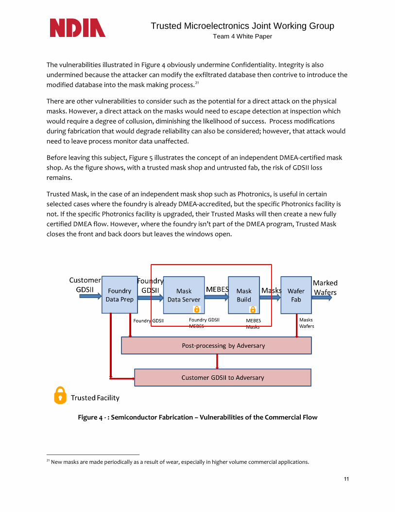
Figure 4 illustrates the vulnerability of a commercial flow, without DMEA security protections. In this case, the customer GDSII is either directly available after it’s decrypted prior to Foundry Data Prep, or it can be extracted by post-processing, at every step of the process.
For example, MEBES is checked against GDSII using various utilities to post-process the MEBES database. Downstream, reticles are routinely inspected with SEMs. The scanned images are in Tagged Image File Format (TIFF) or Bitmap Image File (BMP) format and from there can be converted to MEBES or GDSII. Finally, potential loss of material at the wafer fab is yet another vulnerability because devices can be delayed and imaged to reconstruct GDSII.
20 Examples of the prepping process include: Optical Proximity Correction (OPC), a photolithography enhancement technique commonly used to compensate for image errors due to diffraction or process effects; and Area Fill to control metal density across the die to create good planarization.
Figure 3: Semiconductor Fabrication - The Trusted Flow
11
Trusted Microelectronics Joint Working Group Team 4 White Paper
The vulnerabilities illustrated in Figure 4 obviously undermine Confidentiality. Integrity is also undermined because the attacker can modify the exfiltrated database then contrive to introduce the modified database into the mask making process.21
There are other vulnerabilities to consider such as the potential for a direct attack on the physical masks. However, a direct attack on the masks would need to escape detection at inspection which would require a degree of collusion, diminishing the likelihood of success. Process modifications during fabrication that would degrade reliability can also be considered; however, that attack would need to leave process monitor data unaffected.
Before leaving this subject, Figure 5 illustrates the concept of an independent DMEA-certified mask shop. As the figure shows, with a trusted mask shop and untrusted fab, the risk of GDSII loss remains.
Trusted Mask, in the case of an independent mask shop such as Photronics, is useful in certain selected cases where the foundry is already DMEA-accredited, but the specific Photronics facility is not. If the specific Photronics facility is upgraded, their Trusted Masks will then create a new fully certified DMEA flow. However, where the foundry isn’t part of the DMEA program, Trusted Mask closes the front and back doors but leaves the windows open.
21 New masks are made periodically as a result of wear, especially in higher volume commercial applications.
Figure 4 - : Semiconductor Fabrication – Vulnerabilities of the Commercial Flow

12
Trusted Microelectronics Joint Working Group Team 4 White Paper
Figure 5 - Semiconductor Fabrication – Residual Vulnerabilities with Independent Trusted Mask
13
Trusted Microelectronics Joint Working Group Team 4 White Paper
APPENDIX B – Summary of Team 4 New Methods Review
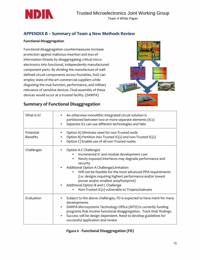
Functional Disaggregation
Functional disaggregation countermeasures increase protection against malicious insertion and loss-of-information threats by disaggregating critical micro-electronics into functional, independently manufactured component parts. By dividing the manufacture of well-defined circuit components across foundries, DoD can employ state-of-the-art commercial suppliers while disguising the true function, performance, and military relevance of sensitive devices. Final assembly of these devices would occur at a trusted facility. (DARPA)
Summary of Functional Disaggregation
What is it? • An otherwise monolithic integrated circuit solution is partitioned between two or more separate elements (ICs)
• Separate ICs can use different technologies and fabs
Potential Benefits
• Option A) Eliminate need for non-Trusted node • Option B) Partition into Trusted IC(s) and non-Trusted IC(s) • Option C) Enable use of all non-Trusted nodes
Challenges • Option A-C Challenges • Incremental IC and module development cost • Newly exposed interfaces may degrade performance and
security • Additional Option A Challenge/Limitation
• Will not be feasible for the most advanced PPA requirements (i.e. designs requiring highest performance and/or lowest power and/or smallest area/footprint)
• Additional Option B and C Challenge • Non-Trusted IC(s) vulnerable to Trojans/malware
Evaluation • Subject to the above challenges, FD is expected to have merit for many developments
• DARPA Microsystems Technology Office (MTO) is currently funding programs that involve functional disaggregation. Track their findings.
• Success will be design dependent. Need to develop guidelines for successful application and review
Figure 6 - Functional Disaggregation (FD)

14
Trusted Microelectronics Joint Working Group Team 4 White Paper
Design Methods
Absence of sensitive logic design is a necessary, but not sufficient, condition for using commercial fabs. For example, if the sensitive IP is stored in encrypted boot files in memory chips on the Printed Circuit Board (“PrCB”), the adversary may be able to deduce the cryptographic key from the IC design. If so, Trusted Foundry and/or special design methods will be required.
Summary of Design Methods Review
What is it? • Design techniques used to prevent reverse-engineering of the semiconductor design and/or prevent reverse-engineering of the design’s correct operation from the design database
Potential Benefits • Several examples are listed below: • E.g. Passive Design Obfuscation
(reference: Prof. Ken Mai, Carnegie Mellon University) • Look-alike gates used to hide logic function;
• E.g. Physically Unclonable Functions (PUF) • A circuit which creates a deterministic, but process-
dependent number; can prevent adversary from learning the device operation even after the device has been successfully RE’d
• Process Specific Function (PSF) (reference: Eakins, et. al., GOMACTech 2017)
• A circuit used to create a chip-unique signature in the EM spectrum. Eakins, et. al. use variation in voltage controlled oscillators (VCO) spectrum
• Potentially used to detect malicious insertions which alter the signature
Challenges • Design obfuscation: deters but doesn’t prevent • PUFs: difficulty of achieving stability across temperature, voltage,
noise, ageing • PSFs: signal/noise ratio
Evaluation • Design Obfuscation: suitable for focused use, if IC not subject to nation-state attack
• PUFs: Ready now. Licensable from Intrinsic-ID, Verayo • PSFs: Research stage
Figure 7 - Design Methods

15
Trusted Microelectronics Joint Working Group Team 4 White Paper
Split Fabrication
Split-fabrication has been proposed as an approach for secure and trusted access to advanced microelectronics manufacturing capability using un-trusted sources. Each wafer to be manufactured is processed by two semiconductor foundries, combining the front-end capabilities of an advanced but un-trusted semiconductor foundry with the back-end capabilities a trusted semiconductor foundry. The security of split fabrication relates directly to a front-end foundry's ability to interpret the partial circuit designs it receives. (Jagasivamani, Gadfort, Sika, Bajura, & Michael, 2014)
Summary of Split Fabrication
What is it? • Front End of Line (FEOL) processing and Back End of Line (BEOL) processing at two different fabs
• Currently the subject of the IARPA Trusted Integrated Chips (TIC) program
Potential Benefits
• Case A) Both fabs are DMEA-certified Trusted Foundries • Can enable technical innovation
• Case B) The FEOL fab is not a Trusted Foundry • Open trusted access to advanced process nodes
Challenges • Technical Challenges • Customers require production-qualified EDA flows, design kits,
physical IP and reliability • Lithography challenges – compatible mask alignment,
registration, etc. (generally requires sharing process information)
• Material compatibility – thermal stress, adhesion, etc. • Business Challenges
• Financial investment, as required to overcome the above challenges
• Legal agreements to enable sharing sensitive information between fabs
Evaluation • Case A may open specialized technical capabilities (not Trust-related) for trailing edge customers within the DMEA Trusted Foundry program
• No visible near-term likelihood for Case B
Figure 8 - Split Fabrication

16
Trusted Microelectronics Joint Working Group Team 4 White Paper
==?
Original GDSII
Design Databas
Fabricated Device
Post-process
Post-process
Equivalence Checking
Equivalence Checking is always carried out using two inputs and result comes out by comparing the functionality of these two input designs. Combinational and sequential equivalence checking are the two methods used today. Combination Equivalence checking is done by making one-to-one mapping of flops between golden design and revised design. Sequential equivalence checkers can verify structurally different implementations which do not have one-to-one flop mapping. (Balakrishnan)
Summary of Equivalence Checking
What is it? • The tapeout GDSII database is compared to the fabricated semiconductor device. The GDSII and/or device are post-processed to enable comparison
• Details • Top layers are delayered with
chemical mechanical planarization (CMP); lower layers with Ga+ FIB
• As each layer is exposed it’s SEM-imaged;
• Key is image repair software • At 14nm, typically ~5 samples are required,
but netlists been reconstructed with a single sample • As a defensive strategy, only reconstruction and compare of
individual layers is required
Potential Benefits
• Reduce risk of malicious insertion during fabrication
Challenges • Cost reduction • Cost estimate: ~$200K for a 5mm x 5mm 14nm die
• Sampling strategy: per-wafer-lot? per-wafer? • Cost reduction • Scalability of delayering service providers
Evaluation • Application of defensive delayering is viable in sensitive programs • Continued development is needed to reduce delaying cost
Figure 9 - Equivalence Checking