true-time delay structures for microwave …
TRANSCRIPT

TRUE-TIME DELAY STRUCTURES FOR MICROWAVE BEAMFORMING NETWORKS IN S-BAND PHASED ARRAYS
A THESIS SUBMITTED TO THE GRADUATE SCHOOL OF NATURAL AND APPLIED SCIENCES
OF MIDDLE EAST TECHNICAL UNIVERSITY
BY KAAN TEMİR
IN PARTIAL FULLFILLMENT OF THE REQUIREMENTS FOR
THE DEGREE OF MASTER OF SCIENCE IN
ELECTRICAL AND ELECTRONICS ENGINEERING
JANUARY 2013


Approval of the thesis:
TRUE-TIME DELAY STRUCTURES FOR MICROWAVE BEAMFORMING NETWORKS
IN S-BAND PHASED ARRAYS
submitted by Kaan TEMİR in partial fulfillment of the requirements for the degree of Master of Science in Electrical and Electronics Engineering Department, Middle East Technical University by, Prof. Dr. Canan Özgen Dean, Graduate School of Natural and Applied Sciences _________________ Prof. Dr. İsmet Erkmen Head of Department, Electrical and Electronics Eng. _________________ Assoc. Prof. Dr. Şimşek Demir Supervisor, Electrical and Electronics Eng. Dept.,METU _________________ Examining Committee Members: Prof. Dr. Canan TOKER Electrical and Electronics Eng. Dept.,METU _________________ Assoc. Prof. Dr. Şimşek DEMİR Electrical and Electronics Eng. Dept.,METU _________________ Prof. Dr. Gönül Turhan SAYAN Electrical and Electronics Eng. Dept.,METU _________________ Prof. Dr. Özlem Aydın ÇİVİ Electrical and Electronics Eng. Dept.,METU _________________ M.Sc. Eser ERKEK REHIS/TTD-MBM, ASELSAN INC. _________________ Date: 31.01.2013

iv
I hereby declare that all information in this document has been obtained and presented in accordance with academic rules and ethical conduct. I also declare that, as required by these rules and conduct, I have fully cited and referenced all material and results that are not original to this work.
Name, Last name : Kaan TEMİR
Signature :

v
ABSTRACT
TRUE-TIME DELAY STRUCTURES FOR MICROWAVE BEAMFORMING NETWORKS
IN S-BAND PHASED ARRAYS
Temir, Kaan M. Sc. Department of Electrical and Electronics Engineering
Supervisor: Assoc. Prof. Dr. Şimşek Demir January 2013, 97 pages
True time delay networks are one of the most critical structures of wideband phased-array antenna systems which are frequently used in self-protection and electronic warfare applications. In order to direct the main beam of a wideband phased-array antenna to the desired direction; phase values, which are linearly dependent to frequency, are essential. Due to the phase characteristics of the true-time delay networks, beam squint problems for broadband phased array systems are minimized.
In this thesis, different types of true-time delay structures are investigated for wideband phased array applications and a tunable S-band true-time delay network having delay over 1ns with high resolution is developed, designed, fabricated and measured. Lower-cost, smaller occupied area, digital/analog control mechanism and ease of implementation are the other features of the developed network.
High delay values with high resolutions for wideband operation are achieved through the combination of several techniques; therefore the desired S-band TTD network is constructed with the synthesis of switched-transmission lines, constant-R networks and periodically-loaded transmission lines. Higher delay states are realized by the switched-transmission lines technique, while the method of constant R-network is used for the intermediate delay states. To increase the tuning flexibility, smaller delay states are accomplished by analog-voltage controlled periodically loaded transmission lines.
A step-by-step procedure is followed during the design process of the S-band true time delay network. Firstly, each method used in the TTD network is analyzed in detail and developed for PCB implementation and the use of COTS components. Then, the designed structures are verified via linear and EM simulations performed by ADS2011®. After that, the effects of production tolerances are examined to optimize each design for S-band operations. Moreover, the designed structures are fabricated by using PCB technology and measured. Finally, a software code is developed in MATLAB to generate the overall cascaded network with the help of measured data.
Keywords: Beam Squint, Delay, Phase Delay, True-Time Delay, Wideband Phased-Array.

vi
ÖZ
S-BANT FAZLI DİZİLERDE MİKRODALGA HUZME YÖNLENDİRME YAPILARI İÇİN
GERÇEK ZAMAN GECİKME YAPILARI
Temir, Kaan Yüksek Lisans, Elektrik ve Elektronik Mühendisliği Bölümü
Tez Yöneticisi: Doç. Dr. Şimşek Demir Ocak 2013, 97 sayfa
Zaman gecikme yapıları kendini koruma ve elektronik harp uygulamalarında yaygın olarak kullanılan geniş bant fazlı dizi anten sistemlerinin en önemli yapılarından bir tanesidir. Fazlı dizilerde ana huzmeyi istenen yöne yönlendirmek için frekansla doğru orantılı faz değerleri gereklidir. Zaman gecikme yapılarının faz karakteristiği geniş bantlı fazlı dizi sistemlerde yaşanan huzme sapması problemlerini en aza indirgemektedir.
Bu tez çalışmasında, geniş bantlı fazlı dizi uygulamaları için çeşitli zaman gecikme yapıları araştırılmış ve S-bandında çalışan, yüksek çözünürlüklü, 1ns üzerinde toplam gecikmeye sahip, ayarlanabilir bir zaman gecikme yapısı geliştirilmiş, tasarlanmış, üretilmiş ve ölçülmüştür. Geliştirilen yapının diğer özellikleri düşük maliyetli olması, küçük boyuta sahip olması, dijital/analog kontrol edilebilmesi ve kolay bir şekilde gerçeklenmesidir.
Geniş bantta, yüksek çözünürlüğe sahip yüksek gecikme değerleri ancak birçok tekniğin bir arada kullanılması yoluyla gerçekleştirilebilir. Bu sebeple, S-bantta tasarlanan TTD yapısı iletim hatlarının anahtarlanması, sabit empedans devreleri ve periyodik olarak yüklenen iletim hatlarının sentezlenmesi ile oluşturulmuştur. Orta seviye gecikme değerleri için sabit empedans devreleri metodu kullanılırken, yüksek gecikme değerleri anahtarlanabilir iletim hatları tekniği ile gerçeklenmiştir. Ayarlama esnekliğini arttırmak için, düşük gecikme durumları analog-voltaj kontrollü periyodik olarak yüklenen iletim hatları kullanılarak başarılmıştır.
Tasarım kısmında, S-bandındaki gerçek zaman gecikme yapısı adım adım geliştirilmiştir. İlk olarak tasarımda kullanılan her bir metot detaylı bir şekilde analiz edilmiş, bu yapılar baskı devre tekniği ve piyasadaki malzemeler kullanılarak üretilmek üzere geliştirilmiştir. Sonraki aşamada tasarlanan yapılar ADS2011® kullanılarak lineer ve elektromanyetik benzetimlerle doğrulanmıştır. Ardından, üretimden kaynaklanabilecek toleransların yapılara etkisi araştırılmış ve her bir yapı S-bandında çalışabilmesi için optimize edilmiştir. Tasarlanan yapılar baskı devre tekniği ile üretilmiş ve ölçülmüştür. Son olarak, elde edilen ölçüm sonuçları kullanılarak MATLAB yardımıyla art arda bağlanan TTD yapısı oluşturulmuştur.
Anahtar Kelimeler: Faz Gecikmesi, Gecikme, Geniş Bant Fazlı Dizi, Gerçek Zaman Gecikmesi, Huzme Sapması.

vii
ACKNOWLEDGEMENTS
I would like to express my sincere gratitude to my adviser, Assoc. Prof. Dr. Şimşek Demir, for his guidance, patience, support and technical suggestions throughout the study. I would also like to thank Prof. Dr. Canan Toker, Prof. Dr. Gönül Turhan Sayan, Prof. Dr. Özlem Aydın Çivi and Mr. Eser Erkek being in my jury and sharing their opinions.
I would like to express my gratitude to Mr. H.Aydın Yahşi for proposing this topic to me and Mr. Murat Sencer Akyüz for providing every support throughout the development of the conducted studies.
I am grateful to ASELSAN A.Ş. for the financial and technical opportunities provided for the completion of this thesis.
I would also like to express my sincere appreciation for Egemen Yıldırım, Kadir İşeri, Damla Duygu Tekbaş, Çağdaş Gücün, Erinç Gücün and Kamil Karaciğer for their valuable friendship, motivation and help.
I would like to thank TÜBİTAK for providing financial support during the study.
Finally, I would like to thank to Tuğçe Serbez for being with me in every moment of this work and giving me the strength and courage to finish it.

viii
TABLE OF CONTENTS
ABSTRACT ..................................................................................................................................... v
ÖZ ................................................................................................................................................ vi
ACKNOWLEDGEMENTS ............................................................................................................... vii
TABLE OF CONTENTS .................................................................................................................. viii
LIST OF TABLES .............................................................................................................................. x
LIST OF FIGURES ........................................................................................................................... xi
LIST OF SYMBOLS ....................................................................................................................... xiii
CHAPTERS
1.INTRODUCTION ........................................................................................................................ 1
1.1 Preface ............................................................................................................................. 1
1.2 A Brief Review of Developments in TTD Networks ........................................................... 2
1.3 Thesis Outline ................................................................................................................... 5
2.FUNDAMENTALS OF TIME DELAY NETWORKS .......................................................................... 7
2.1 Brief Explanation of Time Delay for Phased Array Systems ............................................... 7
2.2 Types of Variable TTD Networks ..................................................................................... 11 2.2.1 Methodologies for TTD Generation................................................................................. 11
2.2.1.a Manipulating The Wave Velocity ............................................................................ 11 2.2.1.b Manipulating the Propagation Distance ................................................................. 16
2.2.2 Control Mechanism for Variable TTD Networks .............................................................. 18
2.3 Design Parameters of TTD Networks and Their Effects in PAA Systems .......................... 19 2.3.1 Operating Frequency and Bandwidth.............................................................................. 19 2.3.2 Insertion Loss over Frequency ......................................................................................... 20 2.3.3 Return Loss over Frequency ............................................................................................ 20 2.3.4 Total Delay Time and Number of Bits .............................................................................. 21 2.3.5 Time Delay Variation over Frequency and RMS Delay Error ........................................... 21 2.3.6 Loss Flatness over Frequency .......................................................................................... 23 2.3.7 Amplitude Imbalance ...................................................................................................... 23 2.3.8 Capacity of Power Handling ............................................................................................ 24 2.3.9 Tuning Speed and Rise/Fall Time ..................................................................................... 24 2.3.10 Size and Power Consumption ....................................................................................... 24 2.3.11 Cost and Complexity ..................................................................................................... 24 2.3.12 Environmental Requirements ....................................................................................... 24
3.DESIGN OF A WIDEBAND TRUE-TIME DELAY NETWORK ......................................................... 25
3.1 Design Requirements for Desired TTD Network .............................................................. 26
3.2 The Types of Transmission Lines and Production Technology Process ............................ 26
3.3 Frequently Used Topologies and Linear Simulations ....................................................... 27 3.3.1 Switched-Transmission Lines Network ............................................................................ 28

ix
3.3.2 Switched-Reflection Lines Network ................................................................................. 30 3.3.3 Periodically Loaded Transmission Lines Network............................................................ 33 3.3.4 Loaded Reflection Lines Network .................................................................................... 34 3.3.5 Constant-R Network ........................................................................................................ 35
3.4 Analysis and Design for Desired TTD Network ................................................................ 39 3.4.1 TTD Design Using Switched-Transmission Lines .............................................................. 39
3.4.1.a Selection of the Substrate ...................................................................................... 39 3.4.1.b Selection of the Switching Elements and Configuration ......................................... 40 3.4.1.c Choosing the Reference Line Length ...................................................................... 46 3.4.1.d Drawings of Each Line and Synthesis of the Layouts ............................................. 47
3.4.2 TTD Design Using Periodically Capacitive Loaded Transmission Lines ............................ 58 3.4.3 TTD Design Using Constant R-Network ........................................................................... 61
4.PRODUCTION OF THE DESIGNED TTD NETWORK AND MEASUREMENTS ................................ 67
4.1 Design of the TTD Network Sections ............................................................................... 68
4.2 Fabrication and Measurement of the Each Designed Section ......................................... 77
4.3 Synthesize of the Cascaded Layout ................................................................................. 81
5.CONCLUSIONS ........................................................................................................................ 83
REFERENCES ................................................................................................................................ 85
APPENDIX
A. DERIVATION AND MODIFICATION OF ALLPASS FILTER CHARACTERISTICS ........................... 87
B. DERIVATION OF PERIODICALLY LOADED HIGH IMPEDANCE LINE CHARACTERISTICS ............ 95

x
LIST OF TABLES
TABLES
Table 3-1: The Requirements for the Desired TTD Network ............................................................. 26 Table 3-2: The Comparison of Different Production Technologies ................................................... 26 Table 3-3: The Comparison of Different Transmission Line Types .................................................... 27 Table 3-4: Properties of the Substrates with High Dielectric Constant ............................................ 40 Table 3- 5: Commercially Available Switches in Market ................................................................... 42 Table 3-6: Widths of Transmission Lines for 50mil RO3210 ............................................................. 47 Table 3-7: CPWG/G Line Lengths for SP4T Switched Lines TTD Network ......................................... 47 Table 3-8: The results of the MSB for SP4T Switched Lines .............................................................. 53 Table 3-9: The results of the 2
nd bit for SP4T Switched Lines ........................................................... 55
Table 3-10: The results of the 3rd
bit for SP4T Switched Lines .......................................................... 57 Table 3-11: Capacitance Range vs Characteristic Impedances in Periodically Loaded Lines ............ 58 Table 3-12: SMD Varactor Diode Products for S-band TTD Design ................................................... 59 Table 3-13: SMD Inductors of COILCRAFT for Lower Inductance ..................................................... 64 Table 3-14: Conductor Widths for 50Ω CPWG/G Lines ..................................................................... 64 Table 4-1: Control Voltages for Desired TTD Network ...................................................................... 67 Table 4-2: Delay Reduction Caused By RO3210 εr Tolerance in Section-1........................................ 68 Table 4-3: Simulation Results for Section-1 ...................................................................................... 71 Table 4-4: Coilcraft RF Chip Inductors@3GHz .................................................................................. 72 Table 4-5: AVX 0402 Package Accu-P Series Capacitors ................................................................... 72 Table 4-6: Selected SMD Components for the Designs of Section-2 and Section-3 ......................... 72 Table 4-7: Simulation Results for Section-2 and Section-3 ............................................................... 74 Table 4-8: Simulation Results for Section-4 ...................................................................................... 76 Table 4-9: Different Arrangements of the Designed Sections for Cascaded Layout ......................... 81 Table A-1: Delay Values for T-section Mutually Coupled Inductors ................................................. 90 Table A-2: Q values for 2
nd Order APF Satisfying Flat Delay over at Least an Octave Band .............. 92

xi
LIST OF FIGURES
FIGURES
Figure 2-1 Comparison of Ideal Phase Shifter and TTD Network ........................................................ 7 Figure 2-2 General Two Port TTD Network ......................................................................................... 8 Figure 2-3 Phase Performance of Group Delay and Phase Delay ....................................................... 9 Figure 2-4 Comparison of Group Delay and Phase Delay ................................................................... 9 Figure 2-5 Wideband PAA System Architecture ............................................................................... 10 Figure 2-6 Varying Signal-Ground Separation ................................................................................... 12 Figure 2-7 Varying Dielectric of a Medium ....................................................................................... 12 Figure 2-8 Varying Capacitive Loading of Transmission Line ............................................................ 13 Figure 2-9 Circuit Representation of a Directional Coupler .............................................................. 14 Figure 2-10 Reflection Type TTD Network with Varying Loads ......................................................... 15 Figure 2-11 Path-Shared Electrical Trombone Line Structure ........................................................... 16 Figure 2-12 Electromechanical Trombone Line Structure ................................................................ 17 Figure 2-13 Conventional Switched–Line TTD Network ................................................................... 17 Figure 2-14 Switched–Lines in a Coupler as TTD Network ................................................................ 18 Figure 2-15 Block Diagram of an Active PAA Transceiver ................................................................. 20 Figure 3-1 TTD Design Flow Chart ..................................................................................................... 25 Figure 3-2 Comparison of SP4T and SP2T Switch Configurations for Switched-Lines ...................... 28 Figure 3-3 Response of 6-Bit SPDT Switched-Transmission Lines ..................................................... 29 Figure 3-4 Response of 6-Bit SP4T Switched-Transmission Lines ..................................................... 30 Figure 3-5 Representation of the Switched-Reflection Lines TTD Network ...................................... 31 Figure 3-6 Response of 6-Bit Switched-Reflection Lines TTD Network ............................................. 32 Figure 3-7 Sample Layout of 4-bit Switched-Reflection Lines TTD Network ..................................... 32 Figure 3-8 Simple Representation of the NLDL Unit Section ............................................................ 33 Figure 3-9 Response of 6-Bit Periodically Loaded Lines TTD Network .............................................. 33 Figure 3-10 Response of the Unit Section for Loaded Reflection Lines Network ............................. 34 Figure 3-11 Delay Response of the Loaded Reflection Lines Network ............................................. 35 Figure 3-12 T-Section Coupled Inductors for 1
st order APF Network ................................................ 35
Figure 3-13 Modified T-Section Coupled Inductors for 2nd
order APF Network ............................... 36 Figure 3-14 The Response of the Unit Cell for APF Network ............................................................ 37 Figure 3-15 The Response of 6-Bit APF TTD Network ....................................................................... 38 Figure 3-16 The Schematic of the Self-Switched 2
nd order APF Circuit ............................................. 39
Figure 3-17 The Effects of Switch Isolation for Switched-Transmission Lines Network ................... 41 Figure 3-18 Pin Descriptions and Truth Table for HMC241LP3 and SKY13384-350LF. ..................... 42 Figure 3-19 Outline Drawings of QFN (16pin, 3x3mm) Package [Dimensions in mm] ...................... 43 Figure 3-20 RO3210 Demo-Board for SP4T Switch Measurements .................................................. 43 Figure 3-21 Measurements of SKY13384-350LF on RO3210 ............................................................ 44 Figure 3-22 Measurements of HMC241LP3 on RO3210 ................................................................... 45 Figure 3-23 The Schematic of 6-Bits Switched-Transmission Lines TTD Network ............................ 46 Figure 3-24 Off-Path Resonance Forbidden Zones for the Reference Lines of SP4T ........................ 47 Figure 3-25 Layout of the Reference Line for the 1
st Bit ................................................................... 48
Figure 3-26 EM Results of the Reference Line for the 1st
Bit ............................................................ 48 Figure 3-27 Layout of the L1 for the 1
st Bit ........................................................................................ 49
Figure 3-28 EM Results of L1 for the 1st
Bit ....................................................................................... 49 Figure 3-29 Layout of the L2 for the 1
st Bit ........................................................................................ 50
Figure 3-30 EM Results of L2 for the 1st
Bit ....................................................................................... 50 Figure 3-31 Layout of the L3 for the 1
st Bit ........................................................................................ 51
Figure 3-32 EM Results of L3 for the 1st
Bit ....................................................................................... 51 Figure 3-33 Layout of the 1
st Bit in SP4T Switched-Lines TTD Network ............................................ 52

xii
Figure 3-34 Co-Simulation Results of the 1st
Bit in Switched-Lines TTD Network ............................ 53 Figure 3-35 Layout of the 2
nd Bit in SP4T Switched-Lines TTD Network ........................................... 54
Figure 3-36 Co-Simulation Results of the 2nd
Bit in Switched-Lines TTD Network ............................ 55 Figure 3-37 Layout of the LSB in SP4T Switched-Lines TTD Network ................................................ 56 Figure 3-38 Co-Simulation Results of the 3
rd Bit in Switched-Lines TTD Network ............................ 57
Figure 3-39 Simple Representation of the Unit Section for Periodically Loaded Line TTD Design ... 58 Figure 3-40 Nonlinear Model of the Varactor, SMV1247-079LF SC-79 ............................................ 59 Figure 3-41 Complete Model of the Unit Section for Periodically Loaded Transmission Line .......... 60 Figure 3-42 Linear Simulation Results for Complete Model of the 4 Sections Loaded Line ............. 60 Figure 3-43 Modeling of the 2
nd order APF Lattice with Short/Open Sections ................................. 61
Figure 3-44 Symmetric Transformation for 2nd
Order APF ............................................................... 62 Figure 3-45 Symmetrical Two-Port Equivalent Circuit for 2
nd Order APF Lattice Circuit .................. 62
Figure 3-46 Pin Descriptions and Truth Table for RFSW1012 ........................................................... 63 Figure 3-47 Measurements of RFSW1012 on RO310........................................................................ 64 Figure 3-48 Layout of One Section Lumped APF Circuit ................................................................... 65 Figure 3-49 Co-Simulation Results of a Single Section Lumped APF Network .................................. 65 Figure 3-50 Effects of 5% Element Tolerances in Lumped APF Circuit ............................................. 66 Figure 4-1 Schematic of the Proposed TTD Network ........................................................................ 68 Figure 4-2 Representation of a Capacitive Loaded Transmission Line .............................................. 69 Figure 4-3 Open Ended Stub Equivalent of a Capacitor .................................................................... 69 Figure 4-4 The Final Layout of Section-1 for Desired TTD Network .................................................. 70 Figure 4-5 The Final Layout of Section-2 for Desired TTD Network .................................................. 71 Figure 4-6 Co-simulation Results for Section-2 and Section-3 with COTS Components ................... 73 Figure 4-7 Delay Variations Due to SMD Components Tolerances for Section-2 and Section-3 ...... 73 Figure 4-8 The Final Layout of Section-4 for Desired TTD Network .................................................. 74 Figure 4-9 Co-simulation Results for Section-4 of Desired TTD Network ......................................... 75 Figure 4-10 Fabricated Sections of the Desired TTD Network .......................................................... 77 Figure 4-11 Comparison of Simulation Results and Measurements for Section-1 ........................... 78 Figure 4-12 Comparison of Simulation Results and Measurements for Section-2 and Section-3 .... 79 Figure 4-13 Comparison of Simulation Results and Measurements for Section-4 ........................... 80 Figure 4-14 Performance of the TTD Network for Different Layout Arrangements ......................... 81 Figure A-1 Delay Characteristics of a 1
st Order APF .......................................................................... 88
Figure A-2 Circuit Representations of a 1st
Order APF Network ....................................................... 88 Figure A-3 Delay Response of T-Section Mutually Coupled Inductors .............................................. 89 Figure A-4 Magnitude Response of T-Section Mutually Coupled Inductors ..................................... 90 Figure A-5 Delay Characteristics of a 2
nd Order APF ......................................................................... 91
Figure A-6 Circuit Representations of a 2nd
Order APF Network ...................................................... 92 Figure A-7 Delay Response of T-Section Mutually Coupled Inductors .............................................. 93 Figure A-8 Magnitude Response of T-Section Mutually Coupled Inductors ..................................... 94 Figure B-1 Schematic of Periodically Loaded Transmission Line ....................................................... 95 Figure B-2 The Effects of Tuning Ratio on Insertion Loss for NLDL ................................................... 96 Figure B-3 The Effects of Tuning Ratio on Delay Performance for NLDL .......................................... 97 Figure B-4 The Effects of Tuning Ratio on Delay Variations for NLDL ............................................... 97

xiii
LIST OF SYMBOLS
ADS : Advanced Design System APF : Allpass Filter C : Speed of Light 3x10
8 m/s
: Relative permittivity Ka band : The frequencies of 26.5–40 GHz Ku band : The frequencies of 12–18 GHz μr : Relative permeability PET : Piezo Electric Transducer RMS : Root-mean-square S band : The frequencies of 2–4 GHz SMD : Surface Mount Device SOLT : Short-Open-Load-Thru SPDT : Single Pole Double Throw SP4T : Single Pole Four Throw TTD : True-time delay UWB : Ultra-wide band X-band : The frequencies of 8–12 GHz VCO : Voltage controlled oscillator Vp : Phase velocity : Relative time delay


1
CHAPTER 1
INTRODUCTION
1.1 Preface
The concept of phased-array antenna (PAA) system, widely known as “smart antenna” in literature, is one of the most promising technologies in modern military applications, in particular frequently being used for both radar and electronic warfare (EW) functions. In details, smart antennas employ a set of antenna elements that are spatially arranged in the form of an array and the signals from these elements are electrically combined to form a steerable beam pattern.
The most attractive parameter for advanced future EW and radar systems based on active PAA is high angle resolution which can be used in precise location-finding, tracking and electronic countermeasure (ECM) techniques while keeping the weight and size of PAA as low as possible. High angle resolution requires ultra wideband (UWB) systems that process ultra short pulses in the time domain which correspond to ultra wide bandwidth in the frequency domain at very low energy levels.
In PAA systems, the incident pulse reaches different antenna elements at different times as a function of incident angle. In early examples of PAA systems, the time difference had been compensated in each channel assigned to each antenna element, to align all the received signals for coherent addition, using digitally controlled phase shifters which are suitable to use rather small bandwidths. Since latest EW systems require larger signal bandwidth, a true time delay (TTD) approach is essential because the phase shifter approach cannot be used due to the beam-squinting effects which drastically influence the performance of the system such as changing of the beam direction and side lobe levels [1].
Ideally a time delay network is a two port device that applies a specific delay to the signal at its input and provides a flat delay characteristic throughout the operating frequency band. The usage of time delay instead of phase shift, offers an enhanced instantaneous bandwidth with fewer occurrence of the beam-squinting effects in comparison, however the realization of time delay circuits offering a flat response in frequency, is a challenging issue for broadband applications. Moreover, the size and cost of time delay circuits are other critical design constraints due to huge number of elements in PAA systems. Many studies have been conducted to develop structures which offer broadband time delay characteristics for over a few decades, resulting lots of new techniques and wide variety of time delay networks. Most of these studies have been focused on either low delay values with high resolutions covering UWB, up to Ka band, or high delay values with low resolutions covering an octave band.
The study conducted in this thesis is mainly concentrated on developing a tunable 2-4GHz TTD network having higher delay values with high resolution, which is essential for practical broadband PAA applications. To design the TTD network, different types of TTD techniques are analyzed in detail for S-band operation and the proper combination of them, including the enhancements for realization, is synthesized. Furthermore, an S-band 6-bit TTD network is fabricated and measured. In addition to this, simulation and measurement results are reviewed in detail.

2
1.2 A Brief Review of Developments in TTD Networks
In broadband PAA applications, delay network realization with a flat response is a challenging issue because it is hard to produce long delays for big antennas. There are several different techniques to design broadband TTD networks in the literature.
One of the basic methods to develop TTD networks is the selection of transmission lines with different lengths using RF switches. The most crucial property of this kind of TTDs is the amount of induced time delay and it is directly proportional to the difference between the physical lengths of the selected paths and the reference path therefore the size of the network is governed by the length of these lines. Besides, TTDs are inherently digital in nature, with 2n lines required for an n-bit system. Moreover, total insertion loss is determined by the type and number of RF switching elements. An advantage of these techniques is that propagation medium characteristics, such as the transmission line characteristic impedance, have insignificant variance for different propagation lengths in TTD networks. Researches about this very primitive TTD Networks were initialized by using N-type germanium crystal diodes as switching elements [2]. In this study, the developed TTD offers a selection of three different channels whose effective length differs by a 1/3 guided wavelength at, X-band and the splitter and combiner parts in between the ports are realized using modified Y-junctions including switching elements. Crystal diodes are biased at very high negative or positive voltages in order to decrease the loss of the network nevertheless the driver circuit of the diodes is rather complex. Moreover size of the overall circuit was not small enough due to the complexity and half-wavelength matching lines.
Over the years, several enhancements have been presented in the manner of improving the performance of the switched-line time shifting. Most of them are based on the innovations on solid-state technology. Solid-state switches such as PIN diodes, field effect transistors (FETs), micro-electromechanical systems (MEMs) switches are emerged and they are used as control elements to select between transmission lines with different lengths [3]-[9]. With the availability of pin diodes, these devices are introduced to TTDs along with discrete switchable lines realized in hybrid packaging using an on-chip continual tunable coplanar delay line at X-band [3]. The function of continual tunable coplanar delay line is the fine tuning of the total delay length, 660ps maximum total delay achieved. The driver circuit requires low voltage (-7 to 0V) however the size of the network (8.32cm) is not small due to longer delay lines.
Parasitic resonance caused by ring like structures of the switched line time shifters is unavoidably exits for ultra wideband systems. The problem was investigated in [4] for switched line TTD networks and it is stated that high switching isolation lessens the effect of resonance to the performance of the switched line circuit. In order to facilitate higher isolation in conjunction with flat delay response, series-shunt diode configuration for switched line structures was proposed in [4]. Considerable interest has been expressed in recent years regarding the use of RF MEMS switches as switching control elements owing to their low insertion loss and high quality factor. Numerous RF MEMS time delay circuits up to 4bits and 100ps time delay have been stated using switched line approach in [5]-[7]. The overall insertion loss for switched delay line technologies increases with the number of bits, providing an inevitable trade-off between delay resolution and insertion loss.
An improvement on switched line time shifter was proposed in [7] where 4-bit MEMS X to Ku-band TTD phase shifters with very low insertion loss, 1.2dB±0.5dB at 10GHz, was released. For the sake of minimizing the loss of the signal path, SP4T switches were used instead of SPDT switches which are conventionally used in switched line time shifter designs. With the use of SP4T switches, number of switches in the signal path is reduced by half which directly decreases the insertion loss.

3
Moreover, it is stated that higher off-state capacitances belongs to semiconductor devices such as GaAs pin-diode or FET switches degrade the bandwidth of TTD phase shifters thus the beam-width of the antenna array. In contrast, the very low up-stage capacitance of series MEMS switches secures wider beam-width so that MEMS switches are appropriate for SP4T approaches in switched line TTD networks. The first 6-bit RF MEMS switched line-time delay circuit was realized for broadband phased array systems operating from DC to 10GHz in [8] with a die area of 27mm x 14mm. With the help of SP4T approach, 393.75ps total delay was achieved with very small delay variations (0.6%) and 1.8±0.6dB insertion loss at 10GHz. To reduce the broadside coupling between closely spaced lines which cause resonance inside the frequency band, parallel lengths of switched lines were minimized. Furthermore; for the benefit of trimming down the physical length of the delay elements in switched line, capacitive loaded transmission lines are introduced instead of meandering transmission lines in [8]. 6–bit RF MEMS TTD circuit was presented with good delay flatness in 7mm x 10mm size however lesser total delay about 60ps was achieved from DC to 18GHz. The presented criteria of selecting proper length for the reference line to avoid half-wavelength resonance is investigated in detail which gives the opportunity of the replacement of series-shunt switching elements with only series elements [9]. Unfortunately; unless some architectural innovations are employed in [10]-[12], the size of the required transmission line to achieve the maximum delay, accuracy and insertion loss, becomes cumbersome for wideband beamformers having huge number of antenna feeding ports. Another drawback of switched-line time delay networks is the incapability of tuning, which is essential to handle variations in manufacturing for mass productions.
When higher accuracy with low loss is needed, varactor-based capacitive-loaded distributed delay line technology is one of most the common solutions. The wave propagation velocity varies by changing the capacitive loading in analog voltage means with the intention of generating required time delay. For fast response, reverse biased Schottky diodes and MEMs varactors are generally used to alter capacitive loading of distributed delay lines. In [13], high impedance transmission lines loaded with GaAs Schottky diodes in the arrangement of distributed LC ladder network was realized to obtain TTD with 360° at 20GHz. The insertion loss of the circuit is about 4.2dB while the size of the circuit smaller than 20mm in length. Instead of Schottky diodes; involvement of MEMs varactors in [14] decreases the insertion loss, lower than 1dB at 30GHz, and the size of the designed circuit, 8mm in length. It is also stated that, power handling capacity and power consumption of MEMs varactors are more beneficial than GaAs Schottky diodes.
As a result of wideband application and selection of different TTD lines, capacitive loaded distributed delay line approach endures a variation of the transmission line characteristic impedance which causes variations on propagation and reflection characteristics for different TTD states. In order to reduce the reflection from these variable elements, λ/4 transmission line sections are needed which results in an increase the dimension of the network. Another drawback is the larger time delay values cannot be realized due to the limitation of varactor capacitance tuning range.
Another solution for TTD structure design is called as dielectric delay line in which the effective dielectric of the transmission line is varied in order to create a true time delay by means of altering the propagation velocity of the wave through transmission. Three types of this approach for microwave application were presented in literature such as liquid crystal delay line (LC), piezoelectric transducer (PET) controlled delay line and compact multi-line phase shifter (MLPS) [15]-[18]. In [15], the orientation of LC molecules was altered via use of a control voltage to change the effective permittivity of the LC substrate; hence true time delay is occurred due to the change of wave propagation velocity. In [16] and [17] a PET controlled dielectric perturber was realized on the top the transmission lines. Altering the bias voltage of the PET adjusts the air gap between

4
transmission lines and dielectric perturber, which affects the effective dielectric constant of the substrate in order to generate true time delay. A novel compact multiline time shifter was established in [18]. The network consists of a uniform composite disc made of a metallic disc and a dielectric disc which can be rotated by a common axis. Microstrip lines in the form of semicircular arcs were printed on the metallic disc while the dielectric disc was divided into two different substrate, εr1 and εr2. The effective dielectric constant of transmission lines is changed by the rotation of the dual disc; therefore the speed of the MLPS is limited by the speed of rotary. 4-channel MLPS from DC to 2GHz was demonstrated with variable time delay ranges from 0 to 375ps, having insertion loss below 1dB in [18].
As a result, dielectric delay line approach, inherently analog, has the ability of high accuracy however slow response time around few milliseconds and large physical size to crate higher TTD values are the main drawback of dielectric delay line approach.
One of the approaches to design TTD network in literature is the reflection type time shifter (RTTS) method which is based on capacitive loading of coupled and isolated ports of a coupler as given in [18]. A novel, digitally controlled, MMIC 4-bit RTTS was presented for X band operations in [19] which has 90ps max. delay and 8dB max. insertion loss on 3.7mm x 2.7mm chip area. In this work, coupled and isolated ports of the Lange coupler were loaded with transmission lines whose other ends were tapped to ground via 16 Schottky diodes. The total time delay was controlled by the choice of which diode pair biased to on-state. For sake of reducing the reflections, coupled and isolated ports were also terminated by 50Ω loads. The designed circuit suffers from low power handling capacity because of the nature of Schottky diodes. For the benefit of higher accuracy, a purely analog RTTS was developed in [20] which consists of a 3dB quadrature directional coupler loaded with simple series tuned varactor diode circuits. The presented insertion loss was below 0.5 dB throughout 40% of the bandwidth which was achieved by varying the bias voltage of the diodes nevertheless the realized maximum relative delay shift was about only 25ps. Analog RTTS demonstrates more advantageous properties such as no power consumption, ability to compensate the variations caused by fabrication process and unlimited number of bits. Available maximum delay in RTTS was improved up to 560ps in [21] by integration of low-cost 3-bit RTTS for 11.5-13GHz with PAA. Occupied area of the module was about 50mm x 25mm, as three stages were cascaded with 5.5dB±1.75dB of the insertion loss. The pin diodes, whose isolation in reverse biasing is relatively poor, used as switching elements; consequently 3dB hybrid coupler pairs were used to guarantee better return loss for wider bandwidth.
The physical size of RTTS is generally restricted by the physical length of hybrid coupler which is approximately equal to quarter-wavelength at the center frequency.
Constant-R network is one of the methods to realize TTD structures for wideband phased array applications. This technique consists of switching elements, reference and delay paths. By switching the paths, desired delay of the time shifter is obtained due to the difference between the respective delays of the two paths. In general, though transmission line is used to realize reference path, delay paths can be modeled with constant-R network which based on an all-pass filter topology with frequency independent unity gain and linear phase response. Common allpass filter topology contains series mutual coupled inductances, bridging capacitance and shunt capacitance. Magnus Danestig and Aziz Ouacha [22] improved the conventional constant-R network and presented a novel topology to realize small size, self-switched time shifter. In this study, it is stated that the number of switching elements should be minimized in order to decrease the loss of conventional constant-R network time shifter based on SPDT switches. In addition this modification helps to decrease the size of the time shifter compared to conventional constant-R network. The new concept was based on transforming the constant-R network into a self-switched

5
network which involves a short transmission line as one state and an allpass delay network as the order. To achieve this requirement, bridging capacitance of classical constant-R network was replaced by a gate voltage controlled field effect transistor switch (SFET1) which acts as a capacitance during off-state and a low resistance during on-state. Moreover, an additional SFET2, driven complementary to SFET1, was added to the end of shunt capacitance of the self-switched constant-R network to minimize the reflections of the network during off-state for wide bandwidth.
A MMIC 5-bit time shifter with operation range of 2-18GHz based on constant-R network was proposed in [23]. The most significant three bits of time shifter was implemented by conventional constant-R network with SPDT switches whereas the other two bits were realized by self-switched one. The circuit, fabricated on 3.90mm x 1.95mm area achieved 46.5mm electrical delay length in air and 11dB±2.3dB transmission loss throughout 2 to 18GHz band.
A 2-20GHz 6 bit TTD with a maximum delay of 145ps was presented in [24]. Due to limitation of the maximum achievable delay for a single section constant-R network at 20GHz, which is approximately 16ps, the produced time shifter had the three least significant bits with self-switched constant-R network and the three most significant bits with SPDT based constant-R network. The spacing between Microstrip lines were arranged carefully to establish the coupled inductance and FET dimensions were selected to ensure flat time delay. 6 bit TTD circuit implemented on 4.0mm x 1.4mm area, results in 2.25ps RMS delay error from 2 to 20GHz.
1.3 Thesis Outline
This thesis is organized in five chapters as follows:
Chapter 2 presents the fundamentals of true time delay networks for wideband operations. Definition of the group delay and phase delay are explained in detail; subsequently the difference between these terms is expressed for phased array applications. Types of variable TTD network are classified in terms of design methodology and control techniques along with pros and cons. Furthermore, requirements to design wideband variable TTD networks are introduced and the effects of these design parameters on PAA systems are discussed briefly.
In Chapter 3, design of a wideband TTD structure is studied. Firstly, specific values are assigned to the design requirements, defined in Chapter 2. Then, common topologies to design a broadband variable TTD are described and each topology is analyzed theoretically besides basic simulations performed by ADS2011®. Finally, three different topologies are improved to form a wideband TTD network satisfying the requirements and complete design steps of each one are given in detail.
Chapter 4 covers the synthesis, fabrication and validation steps of designed structures such as preparing appropriate layouts with the help of EM simulations and comparing the measurement and simulated results of the produced circuitries. Cascading of the designed bits to form a compact structure and measurements results of the overall TTD network are also presented in this chapter.
Finally, chapter 5 presents the conclusions of this thesis work and recommendations for future works to improve the performance of the design.


7
CHAPTER 2
FUNDAMENTALS OF TIME DELAY NETWORKS
The purposes of this chapter are to investigate the nature of the true-time delay for wideband phase array applications and to define the ways of obtaining broadband time shifts in general sense. Moreover, required design parameters of a TTD network for wideband PAA systems are given and the effects of these parameters to PAA systems are examined in this chapter .
2.1 Brief Explanation of Time Delay for Phased Array Systems
In physics, delay is defined as the required time for a signal to travel between two points in a circuit or for a wave to travel between two points in space. Due to the law of nature, all networks having input and output ports, induce some delay characteristics when signals are passed through them. However, a few of them have useful delay performance, constant delay over a significant frequency band, for time shifting named as True-Time Delay (TTD) network.
Figure 2-1 shows the phase characteristics of an ideal phase shifter and ideal TTD network with a time delay ( ) with respect to frequency, under the assumption of both of them have unity gain. Ideal phase shifter has a constant phase performance independent from frequency; however ideal TTD network has a linear phase response directly proportional with frequency.
Figure 2-1 Comparison of Ideal Phase Shifter and TTD Network
There exist two different delay definitions related to the TTD network, one of them is the group delay while the other one is the phase delay.
Group delay, commonly known as envelope delay, is a measure of the time delay of the amplitude envelope of a signal containing various sinusoidal components, through a network. It can be expressed as a useful measure of time distortion, and calculated by differentiating the phase response of the network transfer function with respect to frequency. In other words, the group delay is a measure of the slope of the phase response at any given frequency. It is often desirable

8
for the group delay to be constant across all frequencies otherwise there is temporal smearing of the signal. Constant group delay can be achieved if the transfer function of the network has a linear phase response. The degree of nonlinearity of the phase indicates the deviation of the group delay from a constant value.
Similarly, phase delay is a measure of the time delay but it is dependent on the phase of each sinusoidal component instead of the delay of the amplitude envelope. That is to say, the phase delay gives the time delay in seconds experienced by each sinusoidal component of the input signal.
The difference between phase and group delay is emphasized by analytical derivation of a TTD network having transfer function, H(s), as shown in Figure 2-2. When the network is driven by a quasi-sinusoidal signal, the effects of group and phase delays are observed at the output as follows:
H(S)xin(t) yout(t)
input output
Figure 2-2 General Two Port TTD Network
Define an input signal, xin(t), of which amplitude envelope changes slowly with respect to the rate of change of phase of the carrier sinusoid as
where a(t) is the time dependent amplitude of the envelope and is the carrier frequency.
The output of such an LTI system, yout(t), can be written as
where , is the phase response of and is the frequency.
If is approximately linear over the modulation bandwidth with the definition
Then the output of the LTI system is expressed as

9
where g(t) is the result of integral operation
As a result, delays of the network are defined as
In a network having linear phase response as shown in Figure 2-1 both group and phase delay are constant and equal to the same overall delay of the network. Nevertheless the state of constant group delay does not necessarily result in the same amount of phase delay as a result of nonlinear phase responses due to the effect of phase distortion in TTD networks. Therefore TTD networks having same group delay characteristics can generate different phase delays for a defined frequency band as shown in Figure 2-3 and Figure 2-4.
Figure 2-3 Phase Performance of Group Delay and Phase Delay
Figure 2-4 Comparison of Group Delay and Phase Delay
In phase array systems, instead of group delay, phase delay is one of the most critical parameters for wideband applications. To construct a beam in the required direction, electromagnetic field components radiating from each array elements, must be in phase in given direction. To satisfy this condition for wideband operation, time delay networks are used as given in Figure 2-5.

10
Figure 2-5 Wideband PAA System Architecture
Beam pattern for the given linear phased array system in [25] can be expressed as
where
In order to direct beam with an angle of , the delay values for each element, , must be arranged as
By comparing equation (2.4) and (2.5), it is stated that the required delays for phased array are the phase delay of the TTD network, not the group delay. In the rest of this thesis, delay terminology is only used for phase delay parameter.

11
2.2 Types of Variable TTD Networks
Classification of variable TTD networks can be divided into several categories in literature. In this thesis, these TTD networks are investigated in two main aspects. One of them is the techniques to generate time delays and the other one is related to the control mechanism of variable TTD networks.
2.2.1 Methodologies for TTD Generation
The time delay associated with any electromagnetic signal is defined as the travelled distance divided by the wave velocity.
Two physical approaches to vary the delay of an electromagnetic wave are manipulating the wave velocity and the propagation distance.
2.2.1.a Manipulating The Wave Velocity
For a lossless media, propagation constant, β, of a transmission line can be expressed in terms of equivalent capacitance,C0, and inductance,L0, per unit length of a transmission line. To manipulate the phase velocity, vp, at least one of them should be varied.
In literature, methods of manipulating the wave velocity is offered as altering four features of networks such as varying signal-ground separation, dielectric constant of a media, capacitive loading of transmission lines and reflection characteristics of couplers.
The distance between ground metal and signal conductor affects the equivalent capacitance of the transmission line. The equivalent per length capacitance, Ceq, between two conductors is expressed as
where ra and rb are the radius of the conductors,
d is the distance between conductors,
k is the Boltzmann’s constant, 1.38066x10⁻²³ J/K.
Voltage controlled PETs are generally used as the controller to vary ground-signal separation, shown in Figure 2-6. Applying different DC voltages will cause the transducer to move down or up, depending upon the polarity of the bias voltage, and consequently change the distributed capacitance of the microstrip line. The capacitance variations correspond to variations in effective dielectric constant, which change the propagation velocity and, thus, the phase delay.

12
Microstrip Line
Ground Plane
d
Input Output
Moving part
Up
Down
Controller
Figure 2-6 Varying Signal-Ground Separation
Higher delay values can be realized to achieve ultra wideband operation where bandwidth is bounded by only the limitation of the transmission line. This TTD network is inherently analog and provides higher time delay resolution; however the alignment of the ground-signal separation should be accurate to minimize the time delay errors. Moreover, huge change in equivalent capacitance causes degeneration of the characteristic impedance which adds extra losses to the network. This method requires complex control circuitry along with relatively high power consumption, which increases the size of the overall network. Disadvantages of low speed, high power consumption and large size make this TTD method inappropriate for PAA systems, which require high scanning speed in small size and low power consumption.
Another way to alter the phase velocity is to change the dielectric media of the network. The phase velocity of the medium is given as
In Figure 2-7, a substrate has a dielectric constant εr1 and thickness H1, and a piece of dielectric material to perturb the electromagnetic field of the transmission line, having dielectric constant εr2 and thickness H3, are combined together with a variable air gap height between them. Moving the dielectric perturber in a direction, causes change in effective dielectric constant as a result of the change of thickness of the air between the dielectrics and generates delay as stated in equation (2.10).
Ground
ε r1 Substrate H1
ε r =1 AIR H2
ε r =1 AIR
ε r2 Perturber H3Forward Backward
Up
Down
Figure 2-7 Varying Dielectric of a Medium
Relative phase delay, , obtained by perturbation is

13
where rela ve permi vity of the medium
rela ve permeability of the medium
e ec ve dielectric cosntant of the non perturbated medium
e ec ve dielectric of the perturbated medium
the length of the microstrip line under perturba on
As another option, periodically capacitive loading of a transmission line modifies the characteristics of the line. As shown in Figure 2-8, equivalent capacitance of the loaded line is controlled by the loading capacitors. In other words, characteristic impedance and phase velocity, hence phase delay, of the equivalent network can be varied by changing the loading capacitances. This network can be modeled as a new transmission line called as non-linear transmission line (NLTL). In a periodic NLTL, a relatively high impedance transmission line is loaded at regular spacing by a series of controlled shunt capacitors.
Two types of techniques are used to load the transmission line periodically. Digital controlled NLTL contains switched bank capacitors, while analog controlled NLTL has varactor diodes serving as voltage-dependent capacitors.
sLline
sCline
Cload
sLline
sCline
Cload
sLline
sCline
Cload
sLline
sCline Ceq
sLline
Ceq
sLline
Periodically Loaded Tranmission Line NLTL
Figure 2-8 Varying Capacitive Loading of Transmission Line
Dispersion relation for the network is expressed in [26] as
where k is the wave number and is the length of transmission line, β is the imaginary part of propagation constant and Ceq is the equivalent capacitance for NLTL network.
Define Lline as the series inductance, Cline as the shunt capacitance of a transmission line section and Cload as the periodically loading capacitance, then

14
The cut of frequency, fBragg, stated in equation (2.13) limits the higher end of the frequency range in which the phase velocity performance is independent from frequency.
For frequencies much lower than fBragg where is much lower than 1, the definition of is approximated as follows:
If the varactor diodes are used as loading capacitances, then relative time delay, of the NLTL which depends on control voltage, is obtained as
where N is the number of NLTL section, is the voltage controlled varactor capacitance and is the minimum varactor diode capacitance.
NLTL networks have compact size, simple circuitry and fast response, which are suitable for PAA systems. These time shifter networks can be controlled by analog circuitry, digital circuitry or both; however maximum delay is limited by the tuning range of loading capacitance and the number of sections. On the other hand, the transmission line characteristic impedance also varies for different delay settings in this method, which is not preferred for low loss TTD networks. Bandwidth of NLTL time shifter is limited by the Bragg cut-off frequency. In order to increase fBragg, smaller loading capacitance and shorter transmission line lengths are required, which cause a decrease in total delay.
As seen from Figure 2-9, when an input signal applied to port 1, the signal is divided between port2 and port3 due to the coupling ratio. The load impedances at these ports determine the reflection characteristics of the power from port2 and port 3. The reflected power from port2 and 3 are recombined at the isolated port of the coupler.
Z0
ZL Z0
ZL
Figure 2-9 Circuit Representation of a Directional Coupler
In order to obtain a variable time delay by using couplers, phase velocity of the signal through the coupler, must be varied by means of varying the load impedances of the ports.
The reflection type TTD networks are realized by using 3dB hybrid couplers with variable reactance at the coupled and through ports while the output is taken from the isolated port as shown in

15
Figure 2-10. By arranging phases of the reflected waves from port 2 and 3, ideally lossless TTD network is obtained at the output. The phase characteristics of the reflection coefficients determine the relative time delay obtained from the network. Varactor diodes are one of the solutions to vary reactance of the reflection ports by adjusting the voltage level applied on the varactor.
The complex reflection coefficient, is given as
where XL : the varying load reactance,
: the characteristic impedance of the transmission lines.
Figure 2-10 Reflection Type TTD Network with Varying Loads
By using equation (2.17), the relative time delay for the TTD network, which is limited by the tunability of the loads, is derived as
where XL,min and XL,max are the boundary values of variable reactance at the loads.
Maximum relative delay is obtained for the condition given as
The bandwidth and the size of the coupler determine the frequency range and occupied area of TTD networks respectively. Moreover, the loss of the TTD network is increased by the parasitic effects of the variable loads.

16
2.2.1.b Manipulating the Propagation Distance
The ways of varying propagation distance to obtain time shift can be categorized in three parts which are electrical trombone lines with path select amplifiers, electromechanical trombone lines and switched-transmission lines. One of the most important advantages of these methods is that propagation medium characteristics do not change while delay values are varied.
The schematic diagram of the electrical trombone lines is featured in Figure 2-11. The circuit is composed of wideband amplifiers and shared path trombone line delay elements. By activating only one of the amplifiers, the physical length of propagation path is varied; hence specific delay value is obtained.
Figure 2-11 Path-Shared Electrical Trombone Line Structure
The maximum achievable delay, , determines the total number of delay sections incorporated in the trombone line. Total time delay can be written as
where
n : the number of trombone line sections, that the signals pass through
: the delay of a trombone line unit
Delay elements in the trombone line are generally realized by using lumped LC elements as a tapped transmission line rather than a microstrip or coplanar approach shown in Figure 2-11.
The choice of inductance, L, and capacitance, C, values is uniquely determined by the characteristic impedance and the required delay resolution for a tapped trombone line unit given by equation (2.21) and (2.22) respectively.
For a fixed delay resolution, the tapped delay version of the trombone line suffers from loss and significant delay variation as the total delay is increased. Moreover the bandwidth of this TTD network is bounded by the path select amplifier bandwidth and fBragg of the unit delay element. To satisfy maximally flat delay response, the highest operation frequency must be much smaller than fBragg.
Propagation distance can be controlled by moving trombone lines with the help of mechanic system as shown in figure 2-12. In practical electromechanical trombone line applications, the trombone lines are folded to fit into a compact mechanical size and semi-rigid coaxial cables are

17
used to minimize the losses [27]. The tuning speed and the overall size of this network are not appropriate for PAA systems.
Figure 2-12 Electromechanical Trombone Line Structure
The switched-lines are one of the most common techniques to realize TTD networks by manipulating travelled distance of the wave. Conventional switched-lines time shifter is composed of two line segments of different length, which are selectively connected to the transmission line as shown in Figure 2-13.
Switch Switch
111 ,, ZL
222 ,, ZL
Figure 2-13 Conventional Switched–Line TTD Network
The different path length between two line segments determines the amount of time delay as stated in equation (2.23). The switched-lines TTD network is dependent only the lengths of lines, consequently it is a simple and stable structure. The delay of the wave on a transmission line is given as
where Li is the physical length, θi is the electrical length and is the frequency.
For a lossless transmission line, the impedance measured at a given position from the load impedance is given as
where

18
The impedance seen from the input is independent from Zc and always equal to the load impedance when the transmission line length is multiples of the half wavelengths as stated in equation (2.24). In switched lines networks, resonances occur in the off line when the line length is a multiple of 0.5λ and the phases of the signal on the line will interfere in a way to reflect much of the incoming power back to the input port that cause a distortion in delay performance.
Main contribution to the loss of this TTD network comes from the switching mechanism of the transmission lines. Several techniques are used to reduce the loss of switching elements in [3]-[12].
Switched lines techniques are also used in reflection type TTD networks as shown in Figure 2-14. The coupled (#3) and thru port (#4) of 90°hybrid coupler are loaded by transmission lines which are tapped to ground via shunt switches, and isolated port (#2) is used as the output where reflected signals from thru and coupled port are combined. By enabling the switches, propagation lengths of the reflected waves are altered.
Figure 2-14 Switched–Lines in a Coupler as TTD Network
2.2.2 Control Mechanism for Variable TTD Networks
TTD networks can be classified as digitally controlled and analog controlled networks in terms of control mechanism.
Analog controlled TTD networks have continuously variable delay control which enables any number of delays to be set in a specified range. However, digitally controlled TTD networks have designated number of delay states and cannot be functioned to supply an arbitrary delay which obstructs to handle process variations for mass productions.
The maximum delay of analog controlled TTD networks is bounded by the nature of the components such as varactors. On the other hand, by using digitally controlled TTD networks, such as switched-lines TTD network, higher time delay values can be obtained.
A truth table, which contains list of bits refer to different time states, exists for digitally controlled TTD networks; while analog controlled TTD networks have control voltage to relative delay transfer curves which are utilized to get the desired delay accurately.
An apparent disadvantage of an analog controlled TTD network is the sensitivity of the time delay in consequence of slight variations in the control voltage such as noise on the control voltage. However a digitally controlled TTD structure is not sensitive to that kind of small variations since

19
the transistors are generally well-turned off below their pinch-off voltage which makes digitally controlled TTD’s delay characteristics mostly indifferent to the weakly regulated control voltages.
In order to design the most suitable TTD networks for PAA systems, researches are still working on combining analog and digitally controlled TTD networks.
2.3 Design Parameters of TTD Networks and Their Effects in PAA Systems
Operating frequency with defined bandwidth, insertion loss, matching over frequency, total delay time and number of bits, time delay variations over frequency, loss flatness, amplitude tracking over different states, capacity of power handling, cost and complexity, tuning speed and rise/fall time, occupied area and power consumption are the key parameters to evaluate the performance of the TTD networks for using in the PAA systems.
These technical parameters are explained and the effects of each one to the PAA systems are discussed briefly in this section.
2.3.1 Operating Frequency and Bandwidth
Ranging resolution, R, for a pulse based system is expressed as
where c is the speed of light and BW is the bandwidth of the pulse.
In order to achieve high range resolution; ultra-wideband operation, which means ultra-short pulses in time domain, is essential in PAA systems. The effects of TTD bandwidth to PAA system bandwidth are analyzed in this part.
As seen from Figure 2-5 , the wave front of the PAA is tilted with an angle θ with the antenna aperture and each received signal has to travel different propagation path length, Li , before it arrives at the antenna aperture. This cause progressive phase shifts, , between the received signals at the PAA aperture, given as
where i=0,1,…,N-1: is the index of an antenna element in PAA system
By using equation (2.27), required progressive phase shift, φi’, to direct the beam towards θ0 at f0 is
obtained as
For narrowband applications phase shifters, which ideally deliver constant phase over frequency, are used to steer the beam towards θ0. However for wideband operation, change in frequency f0 cause a change in steering angle for a constant phase shift as seen from the equation (2.27.b). Hence beam squinting occurs which cause a reduction of the gain in the direction θ0 and limits the usable bandwidth of the PAA system. This problem can be solved by using TTD networks. The required progressive phase shift given in equation (2.27.b) is transferred into progressive time delay, .

20
As stated in equation (2.27.c), progressive time delay required to direct the beam towards is independent from the frequency. In other words, steering angle remains constant while the operating frequency is changed. This phenomenon eliminates the bandwidth restriction for wideband PAA systems.
As a result, bandwidth of TTD networks directly affects the bandwidth of PAA systems and wideband TTD networks are desired for PAA systems, which utilize high range resolution.
For military PAA applications, radars and EW systems generally use the operating frequency up to K-band with wide bandwidth. However the instantaneous bandwidth of these systems is limited by digital signal processing structures. For higher operating frequencies, above C-band, phase shifter can be used to steer the beam while TTD networks are crucial for PAA systems operating below C-band.
2.3.2 Insertion Loss over Frequency
Ideally, TTD network is a two port lossless network which adds a frequency independent time delay to the input at the output. However, it is impossible to realize lossless TTD networks in practice. Increment of number of bits, maximum achievable delay and time delay resolution increase the loss of TTD networks.
TTD networks are located inside the beamformer structures for wideband active phased array transmitters or receivers. As seen from Figure 2-15 , insertion losses of the TTD networks have a small impact on receiver noise figure on receiving path where LNA is dominant and negligible effects on output power of the transmitter path, as the high power amplifiers (HPA) generally worked in saturated mode.
TTD
Figure 2-15 Block Diagram of an Active PAA Transceiver
2.3.3 Return Loss over Frequency
Matching over frequency, indicated with return loss, is one of the important parameters for many RF/microwave components. TTD network are generally used as one of the components inside the phased array beamformers which additionally contain amplifiers, phase shifters, filters, attenuators, power combiners. The return losses of the TTD networks should be kept low enough

21
in order to minimize the degeneration of phase and amplitude performance of the beamformers, having cascaded components.
2.3.4 Total Delay Time and Number of Bits
The number of bits, related to the total number of states, is one of the most important parameters for digitally controller TTD networks. For analog controlled TTD networks, huge number of states can be obtained due to the sensitivity of analog control system.
The ideal relation between the total delay time, max, and the number of bits, n, for digitally controlled TTD networks is
where the time delay resolution of a TTD network
As observed from equation (2.27.c), required delay values for TTD networks depend on the distance between antenna elements, the number of antenna elements and scan angle of the systems. The required tuning range of TTD networks is determined by the maximum and minimum scan angles of PAA systems as denoted in equations.
where N : the number of antenna elements,
: the minimum required delay value for TTD networks,
θres : the scan angle resolution of the PAA system.
Practically, the number of TTD bits, n, which depends on total, min and the desired delay resolution, res, in PAA systems should satisfy the equation (2.28.e).
In order to simultaneously achieve wide scanning range in PAA systems, small delay resolution and large overall delay, which are related to the number of bits, are vital for TTD networks.
2.3.5 Time Delay Variation over Frequency and RMS Delay Error
An ideal TTD element has a constant delay response independent from frequency; however there exists delay errors in the operating bandwidth for practical TTD designs. The effects of delay errors on beam generation in PAA systems are investigated in this part.

22
Assume that TTD networks have delay errors over frequency and shifting the operating frequency from f0 to (f0+ f) results in beam squint in PAA system. Then the equation (2.27.c) for the first delay element can be re-written as
where
: angle of the directed beam @ f0
The phase response of a practical TTD network, given in Figure 2-3, can be approximated by using tangent line approximation in a defined bandwidth. A zero phase response frequency point (fφ=0), is defined from zero to minus infinity for this purpose in [28].
where f is the operating frequency.
Substitute f with f0+ f and divide each side by -2π(f0+ f) and the equation (2.30.a) results in
By using the definition of delay given in the equation (2.2), the equation (2.30.b) is organized as
Use power series expansion for
, and assume that
is much smaller than 1. Then,
equation (2.30.c) is approximated as
If the beam squint angle, , is small enough, then the small argument approximation of trigonometric functions can be used. Replacing the equation (2.30.e) into (2.29) results in
Substituting the term in the equation (2.27.c) into the equation (2.30.f) gives the beam squint angle θ.

23
The equation (2.30.g) shows that beam squint of PAA systems depends on fφ=0 of TTD networks. If TTD networks have higher time delay error over frequency, which gives higher fφ=0 in magnitude, then beam squinting in PAA system occurs as a critical problem.
For ideal phase shifters, fφ=0 goes to minus infinity which results frequency dependent beam squint. On the other hand, fφ=0 of ideal TTD networks is equal to zero which gives zero beam squint in PAA systems.
One of the most important criteria stated in literature to define the delay errors of TTD networks is RMS delay error. For digital TTD networks, RMS delay error is expressed as
where n : the number of delay states
: delay error@state (i)=measured delay@state(i) - theoretical delay value state(i)
As a result, time delay variation over frequency is one of the most important parameters for TTD networks used in wideband PAA systems and TTD networks should have delay responses with minimum delay errors.
2.3.6 Loss Flatness over Frequency
Loss flatness specifies how much the insertion loss can vary over the specific frequency range. Insertion losses of RF/microwave components generally increase when operating frequency is increased which result in degeneration of insertion loss flatness over the operating frequency band. TTD networks are inherently wideband microwave components consequently the variation in insertion loss over frequency is inevitable.
In wideband PAA arrays, loss flatness of the overall systems affects the 3dB bandwidth point. If the insertion loss of TTD networks has a linear relation to the frequency inside the operating band; the contribution of TTD networks to the PAA system loss flatness, can be compensated by other components such as gain equalizers.
2.3.7 Amplitude Imbalance
Amplitude tracking shows the insertion loss performance of TTD networks under different delay setting or states at any specified frequency inside the bandwidth. In wideband PAA systems, all antenna elements are generally driven by the required time delays and the same level amplitude. In some applications; amplitude weighting functions, such as Taylor distributions, are used to reduce the sidelobe levels by tapering the PAA elements. However this approach has well-known effects on the reduction of the peak directivity and broadening of the main beam.
Amplitude imbalance for different delay settings may cause uncontrolled amplitude tapering for wideband PAA receivers that disturb the systems performances in sidelobe levels, directivity and beamwidth. As a result, amplitude imbalance over different delay states should be as low as possible for TTD networks.

24
2.3.8 Capacity of Power Handling
Power handling capability of TTD networks depends on the position of TTD Networks in active PAA systems and the type of applications. As shown in Figure 2-15, TTD networks are commonly placed before the HPAs in transmitters and after the LNAs in receivers. Since the power is distributed between the beamformer arms that feed antenna elements; TTD networks are required to deal with intermediate power levels.
Today’s markets produce ultra-low noise amplifier having OP1dB around a few hundred milliwatts so that power handling capacity around a few hundred milliwatts is appropriate for TTD networks.
2.3.9 Tuning Speed and Rise/Fall Time
Tuning speed is defined as the time consumed to change the state from one to another while rise/fall time is called as dead time of the functionality. In wideband PAA systems, time delay settings are changed for each scan angle as stated in the equation (2.27.c) and high speed scanning is generally desired. Scanning speed of wideband PAA systems is directly related to the switching/tuning time of TTD networks. The technology, the circuit topology and the control mechanism determine the tuning speed performance of TTD networks.
In today’s practical PAA applications, FPGA technology is generally used as controllers which need a few hundred nanosecond process time to update the bit settings. Switching speeds around a few hundred nanoseconds can be a practical goal for TTD network realization.
2.3.10 Size and Power Consumption
The criteria related to the size and power consumption of TTD networks depends on the applications. Huge numbers of antenna elements can be used in wideband PAA systems, which results in high numbers of TTD networks. So the size and the power consumption of TTD networks can create problems for PAA platforms especially in military air platforms. Occupying small area and consuming low power are desired for TTD networks; however the performance of TTD networks can be distorted to satisfy these requirements.
2.3.11 Cost and Complexity
Low cost and simple circuitry are always desired for component designs. In PAA applications, cost may not be a crucial parameter because of available high budget in military applications. On the other hand, the complexity of TTD networks can cause fabrication problems during mass production.
2.3.12 Environmental Requirements
Operating Temperatures and vibration stress defined for PAA systems can affect the performance of the TTD networks. Due to the temperature variations, the insertion loss, the return loss, the total phase delay and the delay error can vary.

25
CHAPTER 3
DESIGN OF A WIDEBAND TRUE-TIME DELAY NETWORK
The flow chart, followed to design a TTD network, is presented by defining each step in Figure 3-1.
In this chapter of the thesis, firstly the TTD network design requirements are defined including the weighting coefficients. Sequently, different types of transmission line technologies and production process are investigated and summarized to design realizable structures. Then, the frequently used topologies to design wideband TTD networks are analyzed and some basic simulation results belong to the topologies, are given in detail. After the literature validation, the proposed wideband TTD network is examined for three different types of techniques including the detailed analysis and design steps. During the design process, MATLAB and ADS tools are used to solve the analytical equations and simulate the designs, respectively. EM analysis and simulation results are also given at the end of this chapter.
Figure 3-1 TTD Design Flow Chart

26
3.1 Design Requirements for Desired TTD Network
The requirements for the TTD Network synthesized in this thesis, are listed in Table 3-1, where detailed information of the design parameters are explained in Chapter 2.3. Note that the weighting coefficients are assigned as “1” for the most important requirement and “8” for the least one.
Table 3-1: The Requirements for the Desired TTD Network
TTD NETWORK REQUIREMENTS Weighting Coefficient
Operating Frequency Range 2-4 GHZ 1
Max Time Delay ≈ 1ns
6 bits / ≈16ps step 2
RMS Delay Error ≤ 10ps RMS 3
Amplitude Imbalance < ± 1.5dB 4
Size Occupied Area <3cm x 8cm 4
Tuning Speed < 1 us 5
Return Loss (Input / Output) ≤ -10dB for all states 6
Insertion Loss < -9dB 6
Loss Flatness ≤ ± 1.5 dB over frequency 7
Control Voltage TTL Compatible
8 (+5V or +3.3V)
3.2 The Types of Transmission Lines and Production Technology Process
Properties for different types of production technology process and transmission lines are summarized in Table 3-2 and Table 3-3, respectively.
Table 3-2: The Comparison of Different Production Technologies
Substrate Min
Width/Space Tolerances
Min. Width/Space
Cost Power
PCB Plastics ±0.5 to ±1 mil 5 mil Low medium
THICK FILM Ceramic, Ferrite ±0.5 mil 3 mil medium medium
THIN FILM Ceramic, Sapphire,
GaAs, Si, Glass, ±0.1 to ±0.5 mil 0.6 to 3.0 mil high medium
LTCC Low-Temp
Co-fired Ceramic ±0.4 mil 4.0 mil medium medium
DBC Ceramic ±1.0 mil 7.0 mil medium high
MONOLITIC GaAs, Si - - High for low
Quantity low

27
Table 3-3: The Comparison of Different Transmission Line Types
MICROSTRIPLINE STRIPLINE
SUSPENDED STRIPLINE
SLOTLINE CPWG Finline
Impedance (Ω) 15-120 15-250 30-150 30-200 20-250 10-400
Frequency Band
VHF-X VHF-X L-Q VHF-Q VHF-Q Ka-G
Achievable Bandwidth (%)
0.1-1000 0.1-1000 0.1-1000 0.1-20 0.1-1000 0.1-
1000
Dispersion Low None None High Low Low
Relative Loss Moderate Moderate Low High High Low
Q factor 250 for dielectric
100 -150 for GaAs, Si
400 500 100 150 500
Cost Low Low Moderate Low Low High
Element Mounting
Difficult for Shunt Poor Buried Fair Difficult
for Series Good Fair
Radiation Low for dielectric High for GaAs, Si
Low Low Medium Medium None
Technology PCB, MMIC, Thin-
Film LTCC, PCB - -
PCB, MMIC,
Thin-Film -
Power Handling
Low Medium Low - - -
Table 3-3 represents that the stripline has excellent isolation between adjacent lines; however poor element mounting makes it unreasonable to use it with SMT components. Besides, the slotline is applicable for narrowband applications while the finline is suitable for very high microwave frequency applications. The effective relative dielectric constant for suspended stripline is close to 1, the dielectric constant of air.
As a result, CPWG and microstripline structures are appropriate for TTD network designs.
3.3 Frequently Used Topologies and Linear Simulations
Common realizable TTD networks are divided into five different topologies in this thesis. Two of them are based on switching line lengths to vary the travelled distance, while the other two synthesize slow-wave structures by periodically loading the structures. The fifth one uses the constant-R circuitry, known as allpass structures in literature, to generate delay values.
All of the topologies stated above, are briefly studied one by one with the help of linear simulations. Moreover, the advantages and disadvantages of these topologies are summarized in the remaining parts.

28
3.3.1 Switched-Transmission Lines Network
Basic architecture schematic and operation principles of conventional switched transmission line topology are explained in section 2.2.1.b of the previous chapter. In this part, the performance of this topology, satisfying the design requirements, is analyzed via linear simulations.
In switched–transmission line circuits, losses of transmission lines can be neglected because of available low-loss dielectric materials and CPWG structures. The types of switching elements and switching strategy determine the loss of this topology. The developments in RF MEMS technologies decrease the loss of a switching element along with the use of SP4T components instead of SP2T to reduce the number of switching elements on the selected path by half in comparison with cascaded bits as shown in Figure 3-2. Another advantage of SP4T structures, more compact size is occupied [7].
Figure 3-2 Comparison of SP4T and SP2T Switch Configurations for Switched-Lines
Relative time delay obtained from this topology is given in equation 2.23 which determines difference between transmission lines. By selecting high dielectric constant substrate and bending the transmission lines properly, occupied area of the TTD network can be minimized. On the other hand this topology is not appropriate for realizing very low delay values, because small value of transmission line length difference distorts the isolation between the switched-paths.
TTD networks having 6-Bit, over 1ns delay with nearly 16ps delay resolution are simulated for both switching types. RO3210, which has εr ≈10.8, 50 mil dielectric thickness with 18um copper thickness, is used as substrate in both analyses while the reference lines are assumed as zero length.
6-sections of SPDT switching type are cascaded where CPWG lines are synthesized as 50 Ohm lines. RF switch models having 0.5 dB loss for S-band are used which is valid in recent microwave product catalogues. Isolation between SPDT ports is assumed as 40dB and all ports are well-matched to 50 Ohm for S-band.

29
Figure 3-3 Response of 6-Bit SPDT Switched-Transmission Lines
As shown in Figure 3-3, total length of the network is equal to the sum of the transmission line lengths, 5040mil, and 12 x (Length of SPDT). The insertion loss of the network is around 6.6dB ± 0.6 dB and the network has very low delay variations.
3-sections of SP4T switching type TTD circuit are cascaded to generate the TTD network. 64-states are divided into 3 sections where the parts in these sections are synthesized as switched 50 Ohm lines.
Ideal switches having 0.8 dB loss for S-band are used which is appropriate with microwave product catalogues. Isolation for SPDT paths is assumed as 40dB and well-matched to 50 Ohm for S-band.

30
Figure 3-4 Response of 6-Bit SP4T Switched-Transmission Lines
Total length of the network is equal to the sum of the transmission line lengths, 5040mil, and 6x (length of SP4T). The insertion loss of the network is around 3.6dB ± 0.6 dB and the network has very low delay variations as shown in Figure 3-4.
3.3.2 Switched-Reflection Lines Network
When an input signal applied to port 1 of hybrid coupler, the signal is divided between port2 and 3 due to the coupling ratio. Load impedances at these ports determine the reflection characteristics of the power from port2 and 3. The reflected power from port2 and 3 are recombined at the isolated port4 of the coupler.

31
Figure 3-5 Representation of the Switched-Reflection Lines TTD Network
By arranging the phases of reflected waves from port 2 and 3 with the help of switching transmission line lengths, TTD network including desired phase delays is obtained at the output. The difference in electrical length of the lines, L, determine the relative time delay obtained from the network which is the twofold of this difference due to reflection characteristics.
TTD network having 6-Bit, over 1ns delay with nearly 16ps delay resolution is simulated by varying the length of short circuited transmission line loads. The 90˚ ideal coupler is synthesized by 6-fingered microstrip Lange coupler where coupling ratio of the Lange coupler is nearly 3dB and insertion loss is nearly 0.2dB.
Pin diodes or SPNT switches is used as switching elements and transmission lines are modeled as microstrip lines with an Alumina substrate εr=9.6 and 25mil in height.

32
Figure 3-6 Response of 6-Bit Switched-Reflection Lines TTD Network
Total length of the network is equal to the sum of the transmission line lengths, 2520mil, and the length of the coupler which is nearly 400mil. The insertion loss of the network is around 0.7dB±0.6dB and the network has low delay variations as shown in Figure 3-6. The performance of the coupler directly affects the performance of the TTD network, so wideband 3dB hybrid coupler should be used in reflective type switched-lines TTD networks.
The loss of the reflection-lines network is lower than transmission type. However, coupler based reflection type switched-line TTD network has a drawback in return loss if high delay values are required. A sample layout including pin diodes in [19] is given in Figure 3-7.
Input Port
Output Port
Pin diodes connected
to ground
Figure 3-7 Sample Layout of 4-bit Switched-Reflection Lines TTD Network

33
3.3.3 Periodically Loaded Transmission Lines Network
The schematic of the periodically capacitive loaded-transmission lines network is shown in Figure 2-8. In this section, TTD network having 6-Bit, over 1ns delay with nearly 16ps delay resolution is simulated by varying the loading capacitances. The capacitance tuning range of the varactor diode, MA46580, is used in linear simulation and it is swept from 0.2pF to 0.8pF. Between the varactor diodes, high impedance Microstrip lines are used, nearly 80Ω with an electrical length, Le, of 32˚ at 3GHz and the line widths and lengths are calculated for 25mil Alumina. For the unit section shown in Figure 3-8, max. 32ps delay with return loss better than -13dB is achieved.
Figure 3-8 Simple Representation of the NLDL Unit Section
32 unit sections are cascaded to obtain overall 1ns delay for the TTD network. The results of the overall network are presented in Figure 3-9.
Figure 3-9 Response of 6-Bit Periodically Loaded Lines TTD Network

34
Total length of the network is equal to the sum of the high impedance transmission line lengths and the length of the diodes which is nearly 2700mil. As seen from Figure 3-9, excellent amplitude imbalance, ±0.2dB, is accomplished, however slightly larger delay variations are obtained for higher delay values as shown in Figure 3-9.
The performance of this prototype depends on the varactor tuning ratio (Cmax/Cmin) which is generally lower than 5. The insertion loss of the network is satisfactory; however due to the loading effect, characteristic impedance of the NLTL changes significantly which causes worse return loss.
3.3.4 Loaded Reflection Lines Network
The unit section representation of the loaded reflection lines network is shown in Figure 2-10 and all equation derivations are expressed in chapter 2.2.1.a.
In this section, TTD network having 6-Bit, over 1ns delay with nearly 16ps delay resolution is simulated by varying the load impedance of the hybrid coupler. In order to adjust the load impedance, reasonable capacitance values for varactor diodes are swept from 0.5pF to 1.4pF. Moreover, 90° hybrid coupler is modeled as 6-fingered microstrip Lange coupler, which has 0.2dB loss, and 1.2nH inductors are used in linear simulations. For the unit section, maximum 44ps delay with return loss better than -13dB is achieved as shown in Figure 3-10.
Figure 3-10 Response of the Unit Section for Loaded Reflection Lines Network

35
If ideal hybrid coupler is used instead of the modeled one, 23 cascaded unit sections are needed to generate delay over 1ns as shown in Figure 3-11.
Figure 3-11 Delay Response of the Loaded Reflection Lines Network
Larger area is occupied due to the cascaded 23 sections where the total length of the network is approximately 22cm and max loss of the network is about 9dB.
3.3.5 Constant-R Network
Constant-R circuit is a way of artificial transmission line realization, based on an allpass filter structure. Ideally, an all-pass filter (APF) is a signal processing filter that passes all frequencies equally, but changes the phase characteristics for various frequencies. They are generally used to compensate for other undesired phase shifts as delay equalizers. The input/output impedance of the ideal APF is independent from frequency, so they are called as constant-R networks in literature.
An APF has a unique property which satisfies ideally lossless network with a required delay in a defined frequency band. Mathematical representation of the circuit is based on Hurwitz Polynomial which is stated in Appendix A. Due to the location of zeros and poles, two different types of APF can be synthesized, one of them is the 1
st order APF and the other one is 2
nd order
APF.
1st
order APF can be modeled by mutually coupled inductors with a unity coupling coefficient displayed in Figure 3-12. The corresponding derivations for 1
st order APF are given in Appendix A.
Figure 3-12 T-Section Coupled Inductors for 1
st order APF Network
MUTIND
C=C1
L=L2
L=L1
K=k
C1
L2
L1
Mutual
Mutual

36
For unity coupling ratio,k=1, inductance and capacitance are denoted as
π
π
where fo is the corner frequency and Zo is the input/output port impedance.
However in practice, spiral inductors can be laid out to yield coupling coefficients in the range of k<0.6 in silicon integrated circuits [30]. Therefore, it is not possible to realize the 1
st order APF
lattice network by satisfying the unity coupling coefficient.
The performance of the t-section coupled inductors model is investigated for various coupling coefficients in Appendix A and the equations are solved via a developed code in MATLAB. As seen from Figure A-3, decreasing coupling coefficient improves the delay performance however matching condition is not satisfied anymore, thus causes an increment in insertion loss. For a suitable matching requirement, flat delay response with an appropriate delay variation is obtained by using mutually coupled t-section network.
The values of L1=L2=0.77nH and C1=1.22pF with k=0.47 achieve 51ps±1ps delay with maximum -13dB return loss, covering L and S-band, which can be used as one of the least significant bits in wideband TTD network designs. Furthermore, lower delay values with wider bandwidth can be obtained by decreasing cut-off frequency. As seen from the Figure A-3 and Figure A-4, the performance of TTD network involving mutually coupled inductors, is easily affected by the change in coupling ratio. Variations due to the manufacturing of the circuits cause to distort the desired performance of the TTD network. Moreover, the circuit has no tuning sensitivity after the production process, because mutually coupled inductors are generally printed as coupled microstrip lines [30].
The 2nd
order APF is defined in terms of a quality factor, Q, and a corner frequency, f0, as stated in Appendix A. The delay response of the 2nd order APF is directly controlled by the quality factor while the unity gain is preserved. As seen from Figure A-5; lower Q values generate higher delay variations, nevertheless higher Q values cause an overshot in delay response which is not desired for wideband TTD networks. If maximum 7% delay overshot is allowed, 2
nd order APF gives nearly
150ps delay with a small amount of variation for Q=0.66, which covers S-band. The transfer function of the 2
nd order APF can be modeled by modifying mutually coupled inductors where an
extra parallel capacitance is added as shown in Figure 3-13. The relationships between the elements are derived in Appendix A and the equation (A.11) shows that there exists a solution of k for each Q values to model the 2
nd order APFs.
Figure 3-13 Modified T-Section Coupled Inductors for 2
nd order APF Network
MODIFIED T-SECTION COUPLED INDUCTORS
MUTIND
C
C
LL
Mutual
C2
C1
L1L2
Mutual1
K=k

37
As stated before, approximately 150ps delay can be achieved for Q=0.66 which can be modeled as k=0.387, L1= L2=2.64nH, C1=2.93pF and C2=0.32pF. The delay response of the circuit is 150ps±5ps for the given element values.
If the parallel capacitance, C2, is slightly varied for a defined coupling coefficient; the delay variation of the network is reduced while the insertion loss of the network is increased as shown in Figure A-7. A MATLAB code is developed to solve the element values of modified t-section coupled inductors network for a defined performance parameters related to delay overshot, max. return loss, and delay variation.
For the requirements -20dB maximum return loss, 68ps delay with 0.3ps error is achieved by just reducing C2 from 0.16pF to 0.08pF for k=0.376, L1= L2=1.25nH and C1=1.37pF.
As a result, the modeling of 2nd
order APF is more flexible than the modeling of 1st
order APF, because modified t-section coupled inductors network has two parameters which are the coupling coefficient and parallel capacitance. Variation of the coupling coefficient due to the fabrication process can be compensated by tuning the parallel capacitance, C2 to obtain 2nd order APF response.
The unit cell having available max delay with min. delay overshot and min. delay variation in S-band is synthesized by the developed code.
The values are of k= 0.37, L1= L2=2.5nH, C1=2.1 pF and C2=0.23 pF result in 127ps ± 1.5ps delay with return loss better than -18dB as given in Figure 3-14.
Figure 3-14 The Response of the Unit Cell for APF Network

38
TTD network having 6-Bit, over 1ns delay with nearly 16ps delay resolution is simulated for cascaded 10 sections of APF units. The first four LSB’s is synthesized by a single section while 2 unit sections and 4 unit sections are used to achieve the required delay and matching for the 2
nd MSB
and the MSB, respectively. Furthermore, ideal switching elements, SPDT, and zero length reference lines are used in linear simulation.
The performance of the overall network is shown in Figure 3-15. The insertion loss of the network is lower than 0.3 and the network has low delay variations and low amplitude imbalance, however realization of mutually coupled inductors for microwave frequencies is a challenging topic.
Figure 3-15 The Response of 6-Bit APF TTD Network

39
Mutually coupled inductors can be realized by coupled microstrip lines while SMT capacitors are appropriate for C1 and C2. Another solution is given in [22], where FET switches can be used for small values of C2, to create a self-switching topology as shown in Figure 3-16
C2
C1
Figure 3-16 The Schematic of the Self-Switched 2nd
order APF Circuit
3.4 Analysis and Design for Desired TTD Network
Due the results of the topologies which are linearly analyzed in chapter 3.3, three types of delay structure which have the ability to handle the requirements, are selected to form the desired TTD networks. The switched-transmission lines, periodically loaded high impedance transmission lines and constant-R network are analyzed in detail, developed and designed one by one to satisfy the requirements given in chapter 3.1.
3.4.1 TTD Design Using Switched-Transmission Lines
Switched-transmission line structure is introduced in chapter 2.2.1.b and linearly analyzed in chapter 3.3.1. In this section; the effects of switching elements, parasitics and physical limitations are investigated and the structures are improved.
The steps of the design are divided into five parts.
Selection of the substrate,
Selection of the switching elements and configuration,
Choosing the reference line lengths,
Drawing of each line and EM simulation
Drawing of the overall layout and co-simulation including the effects of the switching elements.
3.4.1.a Selection of the Substrate
The length of a transmission line is directly proportional to the relative dielectric constant as given in equation (3.3), consequently, with the intention of reducing the size of TTD network, should be as high as possible.

40
The use of high-dielectric-constant substrate materials reduces radiation losses because most of the EM field is concentrated in the dielectric between the conductive strip and the ground plane. However, high dielectric-constant substrates suffer from surface-wave effects due to the surface wave coupling, which cause unwanted coupling between the active devices within the structures such as decreasing isolation between paths of the switches. To minimize the effects of surface wave coupling, high isolated switches, should be used.
The commercially available substrates having high dielectric constant are listed in Table 3-4.
Table 3-4: Properties of the Substrates with High Dielectric Constant
Dielectric Constant
Dissipation Factor
Surface Resistivity
Available Thickness
(mm)
50 Ohm Line Width
(εr) (tanδ) (MΩ) (Microstrip)
TMM10 9,2 ± 0,23 0,0022 4x10⁷ [ 0.381 : 12.7 ] 15 – 875 mil
TMM10I 9,8 ± 0,245 0,0020 4x10⁷ [ 0.381 : 12.7 ] 14 – 850 mil
Alumina 9,8 0,0003 1014
[ 0.25 : 1.2 ] 9.4 - 45.7 mil
RO3010 10,2 ± 0,3 0,0022 105 0.13; 0.25; 0.64; 1.28 4.2 – 42 mil
RO3210 10,2 ± 0,5 0,0027 103 0.64; 1.28 22 – 44 mil
RT/Duroid 6010.2LM
10,2 ± 0,25 0,0023 5x10⁶ [ 0.127 : 2.5 ] 4.2 - 90 mil
Moreover, the fabrication tolerances become more severe for higher because the line width is inversely proportional to the . With the purpose of meeting the fabrication criteria; the height of the substrate is increased which creates wider lines and lower ohmic losses. On the other hand, careless handing of thin substrates can cause stress and strain which can modify the performance of the substrate.
To minimize conductor loss, the conductor thickness should be much greater than the skin depth where δcopper≈1.1um at 4GHz.
As a result; the cheap plastic, 1.oz RO3210 with 50 mil height, which is available in ASELSAN stocks, is selected for the design of switched transmission lines TTD network in this thesis.
3.4.1.b Selection of the Switching Elements and Configuration
The critical switching element parameters for the design of TTD network are the isolation between the switching arms, the insertion losses, the return losses and the switching speed.
In the switched-transmission lines TTD network, the resonances can occur in the off-line when the line length is multiples of half wavelengths. This line will appear resonant due to its length, and the phases will interfere in a way to reflect much of the incoming power back to the input port and the performance of the structure is distorted.
In order to minimize the parasitic resonance called as off-path resonance, the switching elements should have enough isolation between their arms. The required switch isolation is investigated for the reference line of the 6-bit S-band SPDT network.

41
Figure 3-17 The Effects of Switch Isolation for Switched-Transmission Lines Network
As seen from Figure 3-17; the isolations of the switch lower than 30dB, degenerate the performance of the TTD network.
The losses due to transmission lines are negligible with respect to the switching element losses, so the performance of the switches determines the network insertion loss as stated in chapter 3.3.1. To satisfy the insertion loss requirement, SPDT switches should have insertion loss lower than 0.6dB while SP4T switches lower than 1.2dB.
The return loss and the switching time for the switches are selected to achieve the requirements given in chapter 3.1
The commercial products available in markets, which satisfy the design requirements, are tabulated in Table 3-5.

42
Table 3-5: Commercially Available Switches in Market
Type IL_max(dB) Return L.(dB) Iso_min(dB) Vcc
SKY13306-313LF SPDT 0.4 16 25 3V
RFSW2100DS (proposed) SPDT 0.4 10 39
SKY13299-321LF SPDT 0.5 16 28 5V
MASW6010G (die) SPDT 0.5 20 30 -5V
MASW-002103-1363 (die) SPDT 0.5 25 50 -15V
RFSW1012 SPDT 0.5 15 28 3.3V
HMC536MS8G SPDT 0.5 15 26 5V
PE42422 SPDT 0.5 18 27 3.3V
PE42552 SPDT 0.65 19 40 3.3V
TGS2304-SCC-(die) SP4T 0.35 21 46 3V
PE42540 SP4T 0.9 18 40 3.3V
MASW4060G (die) SP4T 1 18 40 -5V
AS186-302 SP4T 1 16 40 5V
HMC241LP3 SP4T 1.2 12 30 5V
SKY13384-350LF SP4T 1.2 13 35 5V
In the thesis, SP4T switch configuration is selected for the design process to reduce the number of the switching elements and obtain compact size for the network.
The available components in ASELSAN stocks are the product of Hittite Microwave, HMC241LP3, and the product of Skyworks Inc., SKY13384-350LF.
Both of the products have the QFN (16-pin, 3x3 mm) package and compatible pin configurations as
shown in Figure 3-18 and Figure 3-19.
Figure 3-18 Pin Descriptions and Truth Table for HMC241LP3 and SKY13384-350LF.

43
Figure 3-19 Outline Drawings of QFN (16pin, 3x3mm) Package [Dimensions in mm]
In order to compare the performance of the switches, HMC241LP3 and SKY13384-350LF, a test-board is fabricated on RO3210 50 mil substrate material as shown in Figure 3-20.
Insertion losses, return losses, isolations between the ports and relative delay performances are measured in S-band by using network analyzer.
Figure 3-20 RO3210 Demo-Board for SP4T Switch Measurements
The results are given in Figure 3-21 and Figure 3-22 , respectively. The total insertion loss of the SMA RF connectors is around 0.3dB.

44
Figure 3-21 Measurements of SKY13384-350LF on RO3210

45
Figure 3-22 Measurements of HMC241LP3 on RO3210
Both of the switches have similar performance on 50mil RO3210 substrate. In terms of the insertion losses, HMC241LP3 is slightly better while the port isolations of SKY13384-350LF are nearly 10dB higher at the end of S-band. To minimize the effect of multiples of half wavelength resonance, SKY13384-350LF is selected for the designs of switched-transmission lines network. On

46
the other hand, shared pin configuration and same package size give the opportunity to replace these switches at any time after the fabrication.
In SP4T configurations, the relative delay values, , with respect to the reference lines are
calculated for each section by using the equation (3.4).
where
m : the number for the bits starting from 1 for the MSB and increases up to the LSB.
n : the number for the lines for each bit starting from 1 for the lowest delay line and increases up to the highest one.
: the desired maximum delay value for the TTD network.
For maximum 1024ps delay with 16 ps resolution, the delay values of the 6- bit SP4T switched-transmission lines network are calculated and the schematic is given in Figure 3-23.
512 ps
256 ps
768 ps
0 ps
SKY13384-350LF
128 ps
64 ps
192 ps
0 ps
32 ps
16 ps
48 ps
0 ps
SKY13384-350LF
SKY13384-350LF SKY13384-350LF
SKY13384-350LF SKY13384-350LF
L2
L1
Lref
L3
Most Significant Bit Least Significant Bit2nd
Bit
L2
L1
Lref
L3
L2
L1
Lref
L3
Figure 3-23 The Schematic of 6-Bits Switched-Transmission Lines TTD Network
3.4.1.c Choosing the Reference Line Length
As seen from Figure 3-23, the reference lines are assumed zero in length, however practically it is impossible. The size of the switching elements affects the minimum reference line length.
The reference lines should be selected carefully to get rid of the multiple of 0.5 λ resonance problem. In narrowband application, it is selected as the multiples of half wavelengths are not in the band of interest [9]. However in this thesis, one octave bandwidth is aimed; hence delay lines longer than hall-wavelength cause off-path resonance independent from the reference line length.
For S-band SP4T switch configurations, the required delay values and forbidden zones for the reference line length is plotted in Figure 3-24.
As seen from Figure 3-24, there exist solutions only for the least significant bit where the reference line delay should be smaller than 77ps. For the other bits, off-path resonance problem can be solved with the help of the series junction capacitance of the switches which shifts the resonance frequency. In other words, the switches having high isolation reduce the effects of the off-path resonance for higher delay values.

47
0
100
200
300
400
500
600
700
800
900
1000
0 25 50 75 100 125 150 175 200
De
lay f
or
Ea
ch
Lin
e(p
s)
Reference Line Delay(ps)
The MSB Lines
The 2nd
Bit Lines
The LSB Lines
The Ref. Line
0.5 λ
Resonance λ Resonance 1.5λ
Resonance 2λ
Resonance
Figure 3-24 Off-Path Resonance Forbidden Zones for the Reference Lines of SP4T
3.4.1.d Drawings of Each Line and Synthesis of the Layouts
50Ω Line widths for microstrip and CPWG/G lines are given in Table 3-6 where 50mil RO3210 is used as the substrate. Microstrip line has wider width for 50 Ohm impedance, occupies larger area, while Strip line has element mounting disadvantage. On the other hand, CPWG has the ability to mount the elements easily, such as switches, and the line width can be arranged by changing the ground gap distance which is suitable for IC pad connections.
Table 3-6: Widths of Transmission Lines for 50mil RO3210
Line Width (mil)
Total Height (mil)
Ground Gap (mil)
Length (mil)
Impedance (Ohm)
Delay (ps)
Microstrip Line 43 50 - 70 50,8 16
CPWG/G 13 50 7 79 49 16,2
Stripline 14 100 - 58 50,2 16,1
The CPWG line lengths in each bit are calculated for 50 mil RO3210 substrate as the results of linear calculations.
Table 3-7: CPWG/G Line Lengths for SP4T Switched Lines TTD Network
1st
Bit (MSB) 2st
Bit 3st
Bit (LSB)
Lref (mil) 300 300 300
L1 (mil) 1564 616 379
L2 (mil) 2828 932 458
L3 (mil) 4092 1248 537

48
The bending of transmission lines is done carefully because ring like structures cause parasitic resonance due to the off-state capacitance of switching elements. This parasitic coupling can be suppressed by using high isolated switching techniques and minimizing the closely placed parallel transmission lines. The longer CPWG/G lines are bended to minimize the occupied area for the design where the spacing between the meander lines are arranged as min. three times of the line width to minimize parasitic capacitance effects. The footprint of SKY13384-350LF is regarded while routing the transmission lines.
EM simulations for the lines are done by ADS Momentum tool and all the line lengths are tuned to achieve required delay values. The lower and upper ground planes are connected with conducting ground vias to model the CPWG/G lines. The minimum numbers of ground vias are used during the EM simulation to minimize the complexity of the solutions.
Figure 3-25 Layout of the Reference Line for the 1st
Bit
Figure 3-26 EM Results of the Reference Line for the 1
st Bit

49
Figure 3-27 Layout of the L1 for the 1st
Bit
Figure 3-28 EM Results of L1 for the 1st
Bit

50
Figure 3-29 Layout of the L2 for the 1st
Bit
Figure 3-30 EM Results of L2 for the 1st
Bit

51
Figure 3-31 Layout of the L3 for the 1
st Bit
Figure 3-32 EM Results of L3 for the 1st
Bit

52
Drawings of the delay lines are combined with the footprint of SKY13384-350LF and the overall layout of the MSB is generated as shown in Figure 3-33.
747 mil
11
29
mil
Figure 3-33 Layout of the 1st
Bit in SP4T Switched-Lines TTD Network

53
By adding the s-parameters (s5p) files of SP4T switches, SKY13384; overall performance of the network for the MSB is obtained via ADS co-simulation analysis. The results of the first section are summarized in Table 3-8.
Insertion Loss
Return Loss
Lref
L1
L2
L3
De
lay
(ps)
Figure 3- 34 Co-Simulation Results of the 1st
Bit in Switched-Lines TTD Network
Table 3-8: The results of the MSB for SP4T Switched Lines
Line Length
(mil) Delay(ps) Relative Delay(ps) Insertion Loss (dB)
Lref 338 164 - <2.30
L1 1710 426 262 <2.70
L2 3158 679 515 <2.80
L3 4434 933 769 <3.2

54
The same design procedure is followed for the 2nd
bit of SP4T switched lines network. Maximum delay values up to 192ps are designed with 64ps steps. The overall drawings and EM simulation results are given in Figure 3-35 and Figure 3-36.
62
5 m
il
720 mil
Figure 3-35 Layout of the 2nd
Bit in SP4T Switched-Lines TTD Network

55
Lref
L1
L2
L3
Insertion Loss
Return Loss
Figure 3-36 Co-Simulation Results of the 2nd
Bit in Switched-Lines TTD Network
Table 3-9: The results of the 2nd
bit for SP4T Switched Lines
Line Length
(mil) Delay (ps)
Relative Delay (ps)
Insertion Loss (dB)
Lref 350 164 - <2.3
L1 730 230 66 <2.6
L2 1100 293 129 <2.6
L3 1410 349 185 <2.7
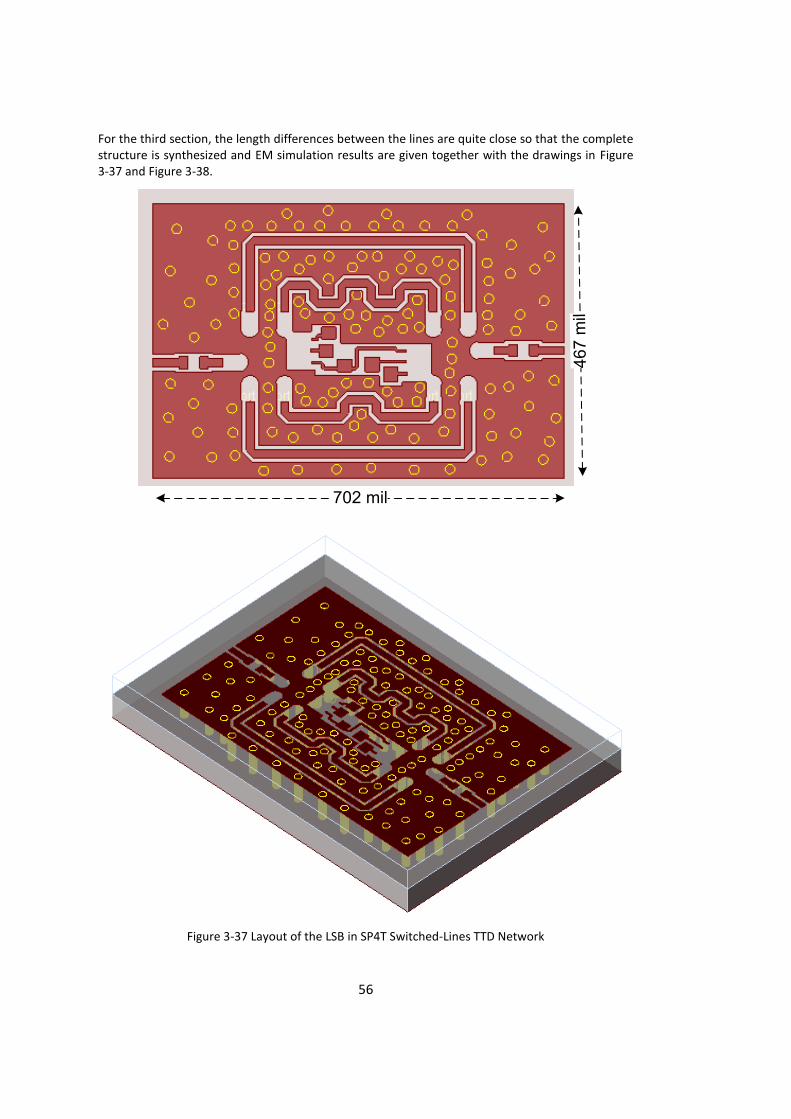
56
For the third section, the length differences between the lines are quite close so that the complete structure is synthesized and EM simulation results are given together with the drawings in Figure 3-37 and Figure 3-38.
702 mil
46
7 m
il
Figure 3-37 Layout of the LSB in SP4T Switched-Lines TTD Network

57
Delay Values of the SP4T Switched Lines for the 3rd
Bit
Lref
L1
L2
L3
Insertion Loss
Return Loss
Figure 3-38 Co-Simulation Results of the 3rd
Bit in Switched-Lines TTD Network
Table 3-10: The results of the 3rd
bit for SP4T Switched Lines
Line Length
(mil) Delay (ps)
Relative Delay (ps)
Insertion Loss (dB)
Lref 363 163 - <2.3
L1 462 181 18 <2.4
L2 540 197 34 <2.6
L3 612 213 50 <2.7

58
3.4.2 TTD Design Using Periodically Capacitive Loaded Transmission Lines
The unit section for the periodically loaded line design is defined as shown in Figure 3-39. The corresponding derivations for the network are given in Appendix B.
The variation of the loading capacitance value should be as small as possible, because the equivalent characteristic impedance of the unit cell is affected due to the loading effect as shown in Figure B-2.
Figure 3-39 Simple Representation of the Unit Section for Periodically Loaded Line TTD Design
Production technology process and transmission line structures limit the characteristic impedance of the lines, which determines the maximum value of the loading capacitance. For return loss better than -13dB, maximum 1.2pF capacitance can be used as the loading capacitance in the unit section produced by PCB technology.
The performance of 5 cascaded unit sections for different characteristic impedances and lengths is investigated in this part. The control ranges of the capacitance and related delay performances are listed in Table 3-11.
Table 3-11: Capacitance Range vs Characteristic Impedances in Periodically Loaded Lines
Z0 (Ω) Le (˚) @3GHz
Range of C (pF)
Tuning Ratio Cmax/Cmin
Average Max. Delay
Delay(ps) Error(%)
120 15 0.29-0.74 2.55 123 6.5
100 17 0.24-0.68 2.83 118 5.1
80 21 0.16-0.64 4.00 125 6.4
The return losses of the desired network better than -13dB and maximum 5% delay variation are regarded as design parameters. In order to minimize the size of the network and realize high impedance values, the substrate with higher dielectric constant and larger height, RO3210 50mil, is selected for the design.
The performance of the varactor diode is critical for periodically loaded transmission line TTD design. Available varactor diode products in markets are listed in Table 3-12.
TLIN TLIN TLIN
C CTL9 TL10 TL11
C4 C3Z=Zo Ohm
E=Le/2
F=F GHz
Z=Zo Ohm
E=Le/2
Z=Zo Ohm
E=Le
F=F GHzC=C pF C=C pF
F=F GHz

59
Table 3-12: SMD Varactor Diode Products for S-band TTD Design
Product Cmin(pF) @ V Cmax (pF) @ V Tuning Ratio
MA46580 0,15 11 V 1,2 1,8 V 8,00
MA46H200/1 0,25 11 V 1 2 V 4,00
MA46410 0,28 11 V 1,2 2 V 4,29
MA46470/1 0,3 11 V 1,1 0,7 V 3,67
MA46H500 0,3 10 V 1 2 V 3,33
SMV2019 0,35 12 V 1,2 2 V 3,43
MA46450/1 0,36 12 V 1,1 0,5 V 3,06
MA46504 0,4 10 V 1 0 V 2,50
SMV1430 0,44 10 V 1,01 0,5 V 2,30
SMV1231 0,49 12 V 1,22 2 V 2,49
SMV1247 0,67 6 V 1,22 2,5 V 1,82
In ASELSAN stocks, the product SMV1247-079LF SC-79 of SYKWORKS INC is available to use in design of the network. The varactor diode is modeled as a non-linear component in Figure 3-40.
Figure 3-40 Nonlinear Model of the Varactor, SMV1247-079LF SC-79
CJO is the variable junction capacitance of the diode and RS is the variable series resistance of the diode. CP is the fixed parasitic capacitance arising from the installation of the die in a package and Ls is the fixed parasitic inductance caused by the package material and the bonding wires in the package.
The complete model for the unit loaded section, including the varactor diode model, input-output port connections and t-junctions, is represented in Figure 3-41. By varying the capacitance of the varactor, SMV1247-079LF SC-79, from 1.1pF to 0.75pF with the help of reverse tuning voltage; 49ps±2ps delay control is achieved for cascaded 4 sections.
Diode
Diode_Model
C
R
L
DIODE1
DIODEM1
C1
R1
L1
Mode=nonlinear
Area=1
Model=DIODEM1
Eg=1.11
Xti=3
Tnom=27
Ffe=1
Af=1
Kf=0
Nbvl=1
Ibvl=0
Nbv=1
Ibv=1e-3
Bv=0
Ikf=0
Nr=2
Isr=0
Fc=0.5
M=M
Vj=Vj V
Cjo=Cjo pF
Tt=0
N=1
Rs=0
Is=1.00e-14
C=Cp pF
R=Rs Ohm
L=Ls nH

60
VarEqn
MSub
VAR
MTEE_ADS
MSUB
MTEE_ADS
MLIN
121226_NLDL_DESIGN 121226_NLDL_DESIGN
MLINMLIN
MLIN MLIN
VAR1
Tee2
MSub1
X3
Tee1
TL25
X2
TL22TL21
TL23TL24
Ls=0.7
L1=67
W1=5
Subst="MSub1"
W1=W1 mil
W2=W1 mil
Dpeaks=
Bbase=
Rough=0 mil
TanD=0.0027
T=35 um
Hu=3.9e+034 mil
Cond=4.7e7
Mur=1
Er=10.8
H=50 mil
Cp=Cp pF
Ls=Ls nH
Rs=Rs Ohm
W3=10 mil
Subst="MSub1"
W1=W1 mil
W=W1 mil
L=L1 mil
W=W1 mil
L=2*L1 mil
Ls=Ls nH
Rs=Rs Ohm
Cv=Cv pF Cv=Cv pF
Cp=Cp pF
Subst="MSub1"Subst="MSub1"
L=5 mil
W2=W1 mil
W3=10 mil
Subst="MSub1"
W=10 mil
L=5 mil
Subst="MSub1"
W=10 mil
Subst="MSub1"
L=L1 mil
W=W1 mil
Figure 3-41 Complete Model of the Unit Section for Periodically Loaded Transmission Line
Cmin
Cmax
Insertion Loss
Return Loss
Figure 3-42 Linear Simulation Results for Complete Model of the 4 Sections Loaded Line

61
If huge numbers of the unit section are cascaded, higher amplitude imbalance is obtained. As a result, realization of the higher delay values by periodically loaded transmission line is not applicable. It is useful for the lower bits due to the analog tuning ability.
3.4.3 TTD Design Using Constant R-Network
TTD networks are usually implemented with the other component such as amplifiers, filters, phase shifters and power combiners/dividers to form beamformer structures in PAA systems. The circuit complexity can affect the performance of coupled structures. Thus, in practical applications mutually coupled inductors are generally not preferred. Although the parallel capacitor added network has more flexibility to the production failures, an extra solution which eliminates the mutually coupled inductors is still needed to realize wideband TTD networks.
Albert Charles Bartlett developed the bisection theorem and the theorem shows that any symmetrical two-port network can be transformed into a lattice network [29].
This network transformation technique is used to model 2nd
order APF network as a wideband TTD network in this thesis. For the 2
nd order APF lattice network shown in Figure A-6; the quality factor,
Q, is defined as
Bartlett bisection theorem is used in reverse direction to transform 2nd
order APF lattice network into a symmetrical two-port network. Due to the Bartlett bisection theorem, a lattice network consists of an open and a short circuited sections as shown in Figure 3-43.
C1
L1
L1
C1
C2C2
L2 L2
C1
L1
L1
C1
C2C2
L2 L2
Short Section
Open S
ection
Open
Section
Zoc
Short
Section
Zsc
Bartlett’s
Theorem
2nd
order APF
Lattice Network
Figure 3-43 Modeling of the 2nd
order APF Lattice with Short/Open Sections
The impedances of the short and open sections for 2nd
order APF Lattice is derived as
The network should be symmetrical to use Bartlett bisection theorem, so open section is divided into two parallel and equal sections as shown in Figure 3-44.
.

62
C1
L1
Network Must be
symmetrical
Divide Open
Secition
2 *L
2
C2
/2
2 *L
2
C2
/2
C1
L1
L2
C2
2 *L2
C2 /2
2 *L
2
C2
/2
C1
L1
Figure 3-44 Symmetric Transformation for 2nd
Order APF
The resultant sections are combined by using the symmetry axis and overall circuit is obtained as shown in Figure 3-45. To complete the Bartlett bisection transformation, the equivalent network must be electrically symmetric which results in
The input Impedance, Zin, of the equivalent two-port circuit for Q=0.707 is given in equation (3.7.b). This equivalent circuit demonstrates constant pure and real impedance that is why it is called as constant R-network.
C1
L1 L1
C1C1
L1
C2
L2
i) L2=L1/ 2
ii) C2=2*C1
2 *L2
C2 /2
(C
2)/2
2*L
2
(C
2)/2
2*L
2
(a) (b)
Figure 3-45 Symmetrical Two-Port Equivalent Circuit for 2nd
Order APF Lattice Circuit
The transfer function of the overall network for Q=0.707 gives the 2nd
order allpass network response.

63
The ideal values of L1=1.4nH, C1=0.34pF and Q=0.707 in symmetrical two-port equivalent circuit achieve 64ps±2ps delay with better than -20dB return loss covering S-band. By changing the corner frequency, 0; lower delay values is obtained.
If L2 and C2 are slightly changed without the necessity of keeping the quality factor exactly same as before, higher delay values with an acceptable insertion loss are obtained.
Define and
where a and b are constants between 0 and 1.
By using cascaded response of the elements with the help of ABCD and Y parameters, input impedance of the network Figure 3-45.b is obtained as
The values of L1=2.7nH, C1=0.57pF, a=0.40 and b=0.62 in symmetrical two-port equivalent circuit reach 129ps±2ps delay with better than -16dB return loss for S-band.
The layout of the single stage network is designed for RO3210 50mil substrate in order to satisfy the compliance between the other designed networks. SP2T switch configuration is selected for the design process and the available SPDT component from Table 3-5 in ASELSAN stocks is the product of RFMD, RFSW1012DS.
Pin descriptions and performance of RFSW1012 which has QFN package (12pin, 2x2mm), are presented in Figure 3-46.
RFSW1012
Figure 3-46 Pin Descriptions and Truth Table for RFSW1012

64
RF1
RF2
RFC
Insertion Loss
Return Loss
Figure 3-47 Measurements of RFSW1012 on RO310
The calculated element values can be realized by using SMD lumped components such as inductor and capacitors. Low inductance values with high SRF are available for the products 0201DS, 0302CS, 0402CS, 0402PA and 0402HP of COILCRAFT which are listed in Table 3-13.
0402 package SMD inductors, which have wider inductance alternatives and can be soldered easily by hand, are selected to draw the layout of the constant-R network. In order to match the line widths to the pad width of 0402 package components and RFSW1012DS, the connection lines are selected as CPWG/G structures.
Table 3-13: SMD Inductors of COILCRAFT for Lower Inductance
Size (mil)
Inductance Range (nH)
Qmin (@ 3GHz)
SRF (MHz)
0201DS 23 x 18 0.5 - 5.5 70 9500
0302CS 34 x 21 0.67 - 5.1 75 9650
0402CS 47 x 25 1.0 - 3.3 80 7000
0402HP 47 x 25 1.0 - 3.9 120 9500
0402PA 47 x 25 0.78 - 3.5 60 8750
In conductor backed co-planar waveguide structures, different line widths are obtained for 50 Ohm impedance by arranging the gap between signal and ground planes.
Table 3-14: Conductor Widths for 50Ω CPWG/G Lines
Line Width (mil)
Ground Spacing (mil)
Impedance (Ohm)
25 20 49.5
10 6 49.0

65
The layout of one section constant-R network is shown in Figure 3-48. While drawing the layout, inductors are separated and placed into the horizontal direction. Furthermore, the capacitors are vertically placed to minimize the size and connection line lengths.
C1 C1
C2
L1 L1
L2
RFSW1012 RFSW1012
334
mil
384 mil
Figure 3-48 Layout of One Section Lumped APF Circuit
By adding the effects of switches, co-simulation for the layout has been done. Subsequently, the element values are tuned with the help of ADS optimization tool in the light of the co-simulation results. For L1=1.1nH, L2=0.86nH, C1=0.18pF and C2=0.9pF; 66ps±4ps delay with return loss better than -18dB is achieved as shown in Figure 3-49.
Ref. Line
APF Section
Insertion Loss
Return Loss

66
Figure 3-49 Co-Simulation Results of a Single Section Lumped APF Network
If the tolerances of lumped components are included to the response of the unit section, then the delay characteristic of the circuit varies as given in Figure 3-50.
Figure 3-50 Effects of 5% Element Tolerances in Lumped APF Circuit
By using cascaded unit sections higher delay values can be obtained, however due to the tolerances of the lumped components; using high number of the components creates uncertainty conditions which may degenerate the performance of the overall network.

67
CHAPTER 4
PRODUCTION OF THE DESIGNED TTD NETWORK AND MEASUREMENTS
Each prototype is analyzed in detail and design procedures related to them are conducted step by step in the previous chapter. Each one has different advantages and disadvantages when the realization of the network is included. To achieve the design requirements listed in chapter 3.1, three types of network are combined together.
The switched-transmission line design is suitable for higher delay bits, because the characteristic of the network is stable and independent from the frequency. High difference between the line lengths can be routed easily to minimize the size. On the other hand, for lower delay values, the length differences between the lines are too close and the reference line length is generally the dominant part to limit the size of the network.
Constant R-network unit section, which is realized by lumped components, is a simple and cheap circuitry and it has a good performance for lower delay values. The performance of the modeled network shows that the circuitry is suitable for middle delay bits. Moreover, it can be tuned easily after the production process by soldering various SMD components. However the variation of the lumped component prevents to create cascaded sections to obtain higher delay values.
The performance of the periodically loaded high-impedance transmission line network is directly affected by the performance of the diode varactors. Only lower delay values can be realized by varying the capacitance of the diode varactors, because the input impedance of the network depends on the loading capacitances. This type of designs is appropriate for the least significant bits. Adding this network to the design gives the flexibility for the overall design, since the amount of delay created by this circuit is controlled via the analog voltage of the diode varactor. In other words, high number of bits, lower resolution and in-time tuning flexibility is achieved with the help of periodically varactor loaded transmission line network.
In order to implement the overall design, a cheap substrate, RO3210 50 mil 1oz, is selected and PCB technology process, available in ASELSAN, is used for the fabrication.
Simple representation of the overall design for S-band TTD is given in Figure 4-1.
Section-1, section-2 and section-3 are controlled via digital voltages while analog voltage is used for tuning section-4.
Table 4-1: Control Voltages for Desired TTD Network
V1 V2 V3 V4 V5
Section-1 0 /3.3V 0 /3.3V - - -
Section-2 - - 0 /3.3V - -
Section-3 - - - 0 /3.3V
Section-4 - - - - 3V to 7.5V

68
512 ps
256 ps
768 ps
0 ps
SP4T SP4T
128 ps
0 ps
SPDT
48 ps
SPDT
64 ps
0 ps
SPDT
Switched Tr Lines
Constant R-NetworksPeriodically
Loaded Line
Section-1
Section-2 Section-3
Section-4
SPDT
Varactors
V1 V2
V3 V4
V5
L2
L1
L3
Figure 4-1 Schematic of the Proposed TTD Network
4.1 Design of the TTD Network Sections
The first section of the network is composed of SP4T switched transmission lines. Details of the design process, simulation results and the designed layout are given in chapter 3.4.1.
There exist some tolerances caused by the fabrication process while realizing the network, which affects the response of the switched-transmission lines section. The sources of these tolerances are given as
The relative dielectric constant of RO3210 substrate : 10.2±0.3
The Height of the substrate : 50±2 mil
Min width /space tolerances for PCB Technology: ±0.5 mil
Min. width /space tolerances and the variation of the substrate height have negligible effects on the delay performance of the section, while characteristic impedance is changed slightly due to the variations which distort the return loss a little. On the other hand, the phase velocity is inversely proportional to the square root of the relative dielectric constant of the medium and any changes in εr directly shifts the delay of the network as stated in equation (2.23).
The designed switched transmission line section in Figure 3-33 is simulated for RO3210 εr variations by ADS co-simulation tool. The dielectric constant variations result in max. 3% delay decrease for each line.
Table 4-2: Delay Reduction Caused By RO3210 εr Tolerance in Section-1
Selected Line
Relative Delay (ps) Change in Delay (ps) Ԑr=10.2 Ԑr=10.8
L1 254 262 8
L2 499 515 16
L3 748 769 21

69
The delay differences listed in Table 4-2 can be compensated by capacitive loading each line which reduce the phase velocity and increase the delay of the lines.
By symmetrically loading λ/4 transmission line, small delay values are obtained as shown in Figure 4-2.
Figure 4-2 Representation of a Capacitive Loaded Transmission Line
The derivation of the delay related to the capacitive loading is given in below. The normalized admittance, b, of the capacitance is defined as
The equivalent delay, e, and equivalent characteristic impedance, Ze, of the line are obtained as
The equation (4.1.b) and (4.1.c) show that delay is increased by increasing the capacitance values, however equivalent line impedance is also increased which cause worse return loss.
For Ω and C=0.3pF, 13ps relative delay with better than -15dB return loss for the loaded line and -20dB return loss for the unloaded line is obtained. One of the realization methods of the shunt capacitance values are open ended stubs. For lower characteristic impedance values, open ended stubs behave like a shunt capacitor as shown in Figure 4-3.
C θ
Z0
Figure 4-3 Open Ended Stub Equivalent of a Capacitor
The relation between the capacitance and open ended stubs is given as
For Z0=43 Ohm, = 14° @3GHz results in 13ps delay tuning range and insertion loss lower than 0.3dB for a loaded line given in Figure 4-2.
Adding open ended stubs increase the flexibility of the section-1 of the designed TTD network. After the fabrication, the relative delay values are tuned slightly by cutting the lengths of stubs where the symmetry of the lines should be preserved. To compensate the overall delay tolerances

70
and keep the symmetry of the layout, 2 open ended stubs are used for L1, while 4 open ended stubs are added for L2 and L3.
The final layout of section-1, synthesized by SP4T switched transmission lines, are given in Figure 4-4.
Open Ended
Stubs
DC Block
Capacitor
QFN (SP4T) QFN (SP4T)
12
18
mil
747 mil
CPWG/G
Lines
Ground
Vias
InputOutput
V1
V2
3.3VV1'
V2'
Figure 4-4 The Final Layout of Section-1 for Desired TTD Network

71
The simulated performance of the designed switched transmission line section is summarized in Table 4-3.
Table 4-3: Simulation Results for Section-1
Lref L1 L2 L3
Control Logic State V1 0 3.3V 3.3V 0
V2 3.3V 0 3.3V 0
Max Delay (ps) 165 440 699 955
Max Relative Delay (ps) 0 274 534 790
Min. Relative Delay (ps) 0 249 502 749
Insertion Loss (dB) -2 ± 0.2 -2.3 ± 0.3 -2.5 ± 0.3 -2.8 ± 0.4
Return Loss (dB) < -12 < -10 < -11 < -9
Rms Delay Error (ps) < 2.8
Max. Delay Overshoot (ps) 3.9
Amplitude Imbalance (dB) < 1.1
Size 18.7mm x 30.5mm
The 2nd
and 3rd
sections of the desired network are based on constant-R network topology given in chapter 3.4.3. The layout and the element values are synthesized for the 3
rd section of the desired
TTD network in chapter 3.4.3. By cascading 2 sections of Lumped APF Circuit; section-2, 128ps delay, is obtained.
The layout of the section-2 is shown in Figure 4-5. In order to generate 128ps delay, the element values are derived including the parasitic of the layout. The optimized lumped element values are L1=L3=1.45nH, L2=L4=0.57nH, C1=C3=0.25pF and C2=C4=0.85pF which result in 130±6ps delay with insertion losses lower than 0.6dB and return losses better than -18dB.
35
0 m
il
530 mil
C1
L1 L1
L2
C1
C2
C3
L3 L3
L4
C3
C4
RFSW1012 RFSW1012input output
Figure 4-5 The Final Layout of Section-2 for Desired TTD Network

72
The optimized inductance values for section-2 and section3 are selected from 0402 package inductors of Coilcraft, while the capacitances are chosen from AVX 0402 package SMD capacitors.
The available chip inductors for the given inductance values are listed in Table 4-4. The inductance tolerances are 5% for all components and the s-parameters are available from the manufacturer.
Table 4-4: Coilcraft RF Chip Inductors@3GHz
Part Number Inductance (nH)
@ 3GHz Q-factor @ 3GHz
SRF (MHz)
0402CS-1N0 0,82 116 12700 0402CS-1N2 1 67 12900
0402CS-1N8 1.83 122 12000 0402CS-1N9 1.66 115 11300 0402CS-2N0 1.95 133 11100
0402HP-1N0 0,81 114 16000 0402PA-0N8 0,75 83 15200 0402PA-1N9 1.92 114 12500
The available 0402 package thin-film chip capacitors with very low tolerances for the calculated capacitance values are listed in Table 4-5. The s-parameters of the parts are available from the manufacturer.
Table 4-5: AVX 0402 Package Accu-P Series Capacitors
Part Number Capacitance
Tolerance (pF)
Self Resonance Frequency
(GHz)
0R1 0.1±0.05 19,4 0R2 0.2±0.05 16,4 0R3 0.3±0.05 14,6 0R6 0.6±0.05 9,5 0R7 0.7±0.05 9,1 0R8 0.8±0.05 8,8 0R9 0.9±0.05 8
The ideal elements are replaced by the s-parameters of the 0402 SMD components listed in Table 4-6. The co-simulation results of realized section-2 and section-3 are given in Figure 4-6.
Table 4-6: Selected SMD Components for the Designs of Section-2 and Section-3
Section-2 Section-3
Ideal SMD Part No Ideal SMD Part No
L1 1.45nH 04CS-1N9 1.10nH 0402CS-1N2
L2 0.57nH 04PA-0N8 0.86nH 0402PA-0N8
C1 0.25pF 0402Accu-P 0R2 0.18pF 0402Accu-P 0R2
C2 0.85pF 0402Accu-P 0R6 0.90pF 0402Accu-P 0R7

73
Section-2: Lref
Section-2: APF
Section-3: Lref
Section-3: APF
Insertion Loss
Return Loss
Section-2
Section-3
Figure 4-6 Co-simulation Results for Section-2 and Section-3 with COTS Components
Coilcraft explains that the 0402 package SMD inductors have 5% tolerance while AVX declares that the 0402 package capacitors are available with 0.05pF tolerances. The Monte Carlo analysis on delay response for section-2 and section-3 is given in Figure 4-7.
m1= 51.04
m2=76.34
m3=106.96
m4=156.94
Figure 4-7 Delay Variations Due to SMD Components Tolerances for Section-2 and Section-3

74
The simulated performance of the designed switched transmission line section is summarized in Table 4-7.
Table 4-7: Simulation Results for Section-2 and Section-3
Section-2 Section-3
Delay (ps) 138 ± 10 68 ± 7
Insertion Loss (dB) < 0.9 < 0.8
Return Loss (dB) < -12 < -15
Amplitude Imbalance (dB) < 0.3 < 0.2
Size 13.3 mm x 8.8 mm 9.8 mm x 8.4 mm
Supply /Control Voltage 3.3 V / High=1.8 V & Low=0V
The fourth section of the desired TTD network is designed by using periodically loaded high impedance transmission line as explained in chapter 3.4.2.
Microstrip transmission lines are used to synthesize 100 Ω high impedance lines because of the minimum width limitation for PCB technology. 9 varactor diodes for the periodically loaded lines are used to realize the required delay values. In order to minimize the size of the section, bends are used for the high impedance line.
Overall view of the layout and co-simulation results including model of varactor diodes are shown in Figure 4-8 and Figure 4-9 respectively. 0402 package 68nH Inductors are used as an RF choke to eliminate the RF signal from DC supply and feed the varactor diodes. The optimization to reduce the delay variation gives the 5 mil line width and 68 mil line length between the varactors. The ground pads of the diodes are connected to the bottom ground with plated vias and the parallel line segments are separated by 20 mil to reduce the parasitic effects.
High Impedance
Line
DC Block
Capacitor
RF Choke
Inductorinput output
Plated Via to
Ground
50Ω50Ω
DC-bias1
85
mil
588 mil
Varactor Diodes
(SMV1247)
Upper Ground
Plane
Figure 4-8 The Final Layout of Section-4 for Desired TTD Network
The modeled capacitances are tuned from 0.7pf to 1.1 pF by decreasing the diode reverse voltage from 5.5V to 2.7V.

75
Cv=1.1pF
Cv=0.7pF
Cv=1.1pF
Cv=0.7pF
Cv=1.1pF
Cv=0.7pF
Figure 4-9 Co-simulation Results for Section-4 of Desired TTD Network

76
The simulated performance of the designed periodically loaded line section is summarized in Table 4-8.
Table 4-8: Simulation Results for Section-4
Periodically Loaded High Impedance Line with 9 Varactors
Delay Range 0 – 50 ps
Insertion Loss < 1.5 dB
Return Loss < -10dB
Delay Variation ± 10 %
Amplitude Imbalance < 1dB
Size 14.7 mm x 4.6 mm
Control Voltage 2.7V to 5.5V

77
4.2 Fabrication and Measurement of the Each Designed Section
The designed sections are fabricated on RO3210 substrate by using LPKF Prototyping Laser System in ASELSAN facilities and the components are assembled on PCBs with the help of reflow soldering technique. The fabricated sections are shown in Figure 4-10.
Section-1: SP4T Switched Transmission Lines
Section-2: Constant-R Network
Section-3: Constant-R Network
Section-4: Periodically Loaded Transmission Line
Figure 4-10 Fabricated Sections of the Desired TTD Network

78
Then, each fabricated section is measured by using Network Analyzer. Before the measurements 2-port SOLT calibration is done for the network analyzer.
Initial measurements for section-1 give the relative delay values of 258ps, 511ps and 774ps. By cutting the open-ended stubs for the longest line of section-1, the relative delay values are tuned. Final measurements are compared with the simulation results for section-1 of the desired TTD network. The delay of the reference line for section-1 is recorded a 300ps.
Figure 4-11 Comparison of Simulation Results and Measurements for Section-1

79
The responses of the fabricated section-2 and section-3 of the desired TTD network are measured. As seen from Figure 4-12, the insertion losses are slightly higher than the expected values while the simulation and measurement results are matched for the relative delay responses. The tolerance of the SMD components and the loss of the RF SMA connectors may have an effect on the higher insertion losses. Moreover, the delays of reference lines are measured as 237ps for the section-2 and 203ps for the section-3.
Figure 4-12 Comparison of Simulation Results and Measurements for Section-2 and Section-3

80
By sweeping the analog bias voltage of the varactor diodes from 3.0V to 7.5V, measurement data are recorded for section-4 of the desired TTD network as shown in Figure 4-13. The insertion losses limit the usable tuning range at the end of the frequency band and the analog voltage tuning range can be used as 3.8V to 7.5V where 7.5V is used for the reference delay setting. Moreover, the delay of reference setting is measured as 241ps.
Figure 4-13 Comparison of Simulation Results and Measurements for Section-4

81
4.3 Synthesize of the Cascaded Layout
The final layout of the desired TTD network is obtained by cascading the fabricated sections in different configurations. In order to achieve optimum RMS delay error and amplitude imbalance for the desired TTD network, the positions of the designed sections are investigated.
The permutation of 4 sections result in 24 different configurations and the simulation results of the sections are evaluated with the help of a developed MATLAB code for 24 configurations. According to the outcome, the results of six different configurations having optimum performance,
are plotted in Figure 4-14.
Table 4-9: Different Arrangements of the Designed Sections for Cascaded Layout
Configuration # ARRANGEMENT OF THE SECTIONS
9 Section-2 Section-3 Section-1 Section-4
13 Section-3 Section-1 Section-2 Section-4
18 Section-3 Section-4 Section-2 Section-1
19 Section-4 Section-1 Section-2 Section-3
20 Section-4 Section-1 Section-3 Section-2
21 Section-4 Section-2 Section-1 Section-3
Figure 4-14 Performance of the TTD Network for Different Layout Arrangements


83
CHAPTER 5
CONCLUSIONS
In PAA applications, especially for military purposes, operation band of the system should be more than octave bandwidth. In order to generate the appropriate beam, one needs to have frequency dependent linear phase shifting throughout the bandwidth avoiding beam deformation and squint. Regular phase shifters fail to satisfy this requirement for wide bandwidth. Therefore, the requirement of TTD’s emerges. Several types of TTD’s which are represented in literature, are analyzed, modified and simulated in this work. Along with defining TTD design parameters, their impact on PAA system’s ability and capability are also mentioned. In the light of these analyses, a TTD network covering S-Band and implying over 1 ns time delay using 6-bits is designed. During the design, 3 types of TTD topologies in the literature are used. Periodically loaded transmission line, constant-R network and switched transmission line are used as building blocks of desired TTD network as least significant bits, intermediate bits and most significant bit, respectively. In transmission line theory, loading of a transmission line alters the characteristics of the transmission line involving time delay response. With the help of this feature, periodically loaded transmission lines are used to impose time delay for a part of desired TTD network. Due to the analyses and simulations; this topology can implement lower delay with a bearable insertion loss and return loss throughout S-band. Consequently, periodically loaded transmission line is an excellent candidate for least significant bits of the desired TTD network. In the design, varactor diodes are used to manipulate the phase velocity as loading elements. These devices give the opportunity of tuning the device for required design parameters. For the sake of best time delay performance, varactor diodes should have a tuning ratio between 3 and 4, however obtaining varactor diodes with this ability is time-consuming, and thus, varactor diodes at ASELSAN stocks, which have a very low tuning ratio in comparison, are used in the design. As a final step, designed structure is manufactured and measured. The resultant figures are in consistent with the design parameters except that varactor diodes begin to degrade at the end of the frequency band. Another reason behind this distortion may be the soldering process of the components. In literature, constant-R networks used to impose time delay involve mutually coupled inductors. In this work, instead of using mutually coupled inductors which have a complicated mass production process, lumped equivalent circuit is proposed. 2
nd order Constant-R network with
lumped equivalent circuit is analyzed and simulated. Results of simulations show that this topology can impose a time delay of nearly 130 ps for one section, and sections may be cascaded to achieve higher delays. In theory, constant-R networks are lossless and perfectly matched nevertheless parasitic effects of lumped component distort the performance of the circuit. Using COTS components, nearly 65 ps of time delay for each section is realized along with insertion loss of 1.8 dB at most which includes the losses of two SPDT switches. The basic structure to generate time delay is altering the propagation path of travelling wave, thus in this work, switched line transmission line topology with small size and low loss is proposed for most significant bits of TTD network. With the help of SP4T switches and meander line method, the size of the circuit can be lowered to a manageable size along with concerning not to distort the signal at each branch. The choice of RO3210 as the substrate significantly reduces the cost of the

84
circuit and enables to route shorter line for higher time delays by reason of high permittivity constant. Another innovative approach to enhance the performance is introduction of open-ended stubs to the transmission lines. This approach eliminates the degradation of delay performance due to the manufacturing tolerances including tolerances of substrate properties. After the fabrication, proposed stubbed transmission line structure gives the opportunity of tuning for best performance. The measured relative delay values are consistent with the simulated results and have a very insignificant time delay variation about 3ps over S-band. With the building blocks of the desired TTD network at hand, a MATLAB analysis has been conducted in order to propose an arrangement of block for the lowest RMS delay error and bearable amplitude imbalance. As a result, the requirements for constructing beam in a S-Band PAA system can be satisfied by the proposed network. For further improvements, reducing the insertion loss and lowering RMS time delay error are most reasonable prospects to investigate. In the issue of insertion loss; introduction of low-loss SP4T switches and substrates for switched transmission lines, modeling of newly emerged self-switched constant-R network with lumped elements and investigation of different manufacturing process for loaded line topology are the most promising topics to start with. Furthermore, lowering RMS time delay error may be achieved using custom designed lumped components with lower tolerances for constant-R network and implementation of varactor diodes with higher tuning range and lower capacitance for periodically loaded transmission line topology.

85
REFERENCES
[1] Yaping Liang, C.W. Domier, and N.C. Luhmann,”MEMS Based True Time Delay Technology for Phased Antenna Array Systems”, Asia-Pacific Microwave Conference, 2007.
[2] E.M.Rutz and J.E.Dye, “Frequency translation by phase modulation”, IRE WESCON Conv. Rec., pt. 1, pp.201-207, 1957.
[3] P. Abele, R. Stephan, M. Birk, D. Behammer. H. Kibbel, A. Trasser, K.-B. Schad, E. Sonmez and H. Schumacher, “An Electrically Tunable True-Time Delay Line on Si for a Broadband Noise Radar”, IEEE, pp.130-133, 2003.
[4] J. Schoebel, J. Schueuer, R. Caspary, J. Sshmitz and M. Jung, “A True-Time Delay Phase Shifter System for Ultra-Wideband Applications”, Microwave Conference (GeMIC), German, 2008.
[5] Gabriel M. Rebeiz, "RF MEMS Theory, Design, and Technology", Joho Wiley & Sons Inc., Hoboken, New Jersey, 2003.
[6] J. B. Hacker, R. E. Mihailovich, M. Kim, and J. D. DeNatale, “A Ka-band 3-bit RF MEMS true-time-delay network,” IEEE Trans. Microw. Theory Tech., vol. 51, no. 1, pp. 305–308, Jan. 2003.
[7] Guan-Leng Tan, Robert E. Mihailovich, Jonathan B. Hacker, Jeffrey F. DeNatale and Gabriel M. Rebeiz, “Low-Loss 2- and 4-bit TTD MEMS Phase Shifters Based on SP4T Switches”, IEEE Transactin on Microw. Theory and Tecn, vol. 51, no.1, January 2003.
[8] Christopher D. Nordquist, Christopher W. Dyck, Garth M. Kraus, Isak C. Reines, Thomas A. Plut, Franklin Austin, Patrick S. Finnegan and Charles T. Sullivan, “A DC to 10-GHz 6-b RF MEMS Time Delay Circuit”, IEEE Microwav. and Wireless Components Letters, vol. 16, no. 5, May 2006.
[9] Christopher D. Nordquist, Christopher W. Dyck, Garth M. Kraus, Charles T. Sullivan, Franklin Austin IV, Patrick S. Finnegan, Mark H. Balance, ”Ku-band Six-bit RF MEMS Time Delay Network”, IEEE CSIC Symposium, Monterey, CA, October 2008.
[10] Ta-Shun Chu, Jonathan Roderick, Hossein Hashemi, “A 4-Channel UWB Beam-Former in 0.13pm CMOS using a Path-Sharing True-Time-Delay Architecture”, IEEE Solid-State Circuit Conference, San Francisco, CA, February 2007.
[11] Ahmet A. Helmy, Kamran Entesari, “Reduced-Size Ultra-Wideband True-Time-Delay Beam-Forming Receivers”, IEEE ISCAS, Rio de Janeiro, May 2011.
[12] Ta-Shun Chu, J. Roderick, H.Hashemi, “An Integrated Ultra-Wideband Timed Array Receiver in 0.13um CMOS Using a Path-Sharing True Time Delay Architecture”, IEEE Journal of Solid-State Circuits, Vol.42, No.12, December 2007.
[13] Jian Qing, Yanling Shi, Wei Li, Zongsheng Lai, Ziqiang Zhu and Peisheng Xin, "Ka-Band Distributed MEMS Phase Shifters on Silicon Using AlSi Suspended Membrane", Journal of Microelectromechanical Systems, Vol. 13, No. 3, pp. 542-549, June, 2004.
[14] T. Kuki, H. Fujikake, H. Kamoda, and T. Nomoto, "Microwave variable delay line using a membrane impregnated with liquid crystal," IEEE MTT-S Digest, pp. 363-366, 2002.
[15] T. Kuki, H. Fujikake, H. Kamoda, and T. Nomoto, "Microwave variable delay line using a membrane impregnated with liquid crystal," IEEE MTT-S Digest, pp. 363-366, 2002.

86
[16] T. Yun, and K. Chang, "A Low-Cost 8 to 26.5 GHz Phased Array Antenna Using a Piezoelectric Transducer Controlled Phase Shifter," IEEE Tran. On Antenna and Propagation, Vol. 49, No. 9, pp. 1290-98, September 2001.
[17] Lu Yang, "Ka-band true time delay E-plane beam scanning and broadening phased array system using antipodal elliptically-tapered slot antennas", IEEEAntennas and Propagation Society International Symposium 2006, IEEE Albuquerque, NM, 2006.
[18] In-Young Lee, Kyoung-Ho Lee, Duk-Yong Kim, Yoon-Yong Kim and Ji-Hae Yea, “A Novel Compact Multi Line Phase Shifter for Precise Array Antenna Beam Control”, IEEE MTTS-S Digest, Vol. 3, pp. 1773-1776, June 2004.
[19] K Wilson, J M C Nicholas and G McDermott, “A Novel MMIC, X-Band, Phase Shifter”, Microwave and Millimeter-Wave Monolithic Circuits, Vol.85, pp.10-14, June 1985.
[20] S. Lucyszyn, I.D. Robertson and A.H. Aghvami, “A High Performance Analogue Time Shifter for Wideband Phased Array Antennas”, IEEE Colloquium on Recent Advances in Microwave Sub-Systems for Space and Satellite Applications, March 1993.
[21] B. Avdijiiski, R. Arnaudov and A. Kostov, “MCM Low-Cost True Time Delay Phase Shifter”, IEEE 28th Int. Spring Seminar on Electronics Technology: Meeting the Challenges of Electronics Technology Process, pp. 58-61, August 2005.
[22] M. Danestig, A. Ouacha, C. Lie Kien Tsoen, T. Tieman and S. Rudner, “Recursive Filters Employing Transmission Type Phase Shifter and Novel Self-Switched Time Shifters for Frequency Tuning”, 28
th European Microwave Conference, Amsterdam, 1998.
[23] A. Ouacha, B. Carlegrim and M. Alfredson, “Ultra Broadband MMIC 5-Bit Time Shifter”, Microwave Conferences, Vol. 2, pp. 242-245, Pacific Asia, November 1999.
[24] John G. Willms, A. Ouacha and Frank E. van Vliet, “ A wideband GAAS 6-BIT True-Time Delay MMIC Employing On-Chip Digital Drivers”, 30
th European Microwave Conference, October 2000.
[25] Hubegt Visser, “Array and Phased Array Antenna Basics”, Wiley 2005.
[26] Jonathan D. Fredrick, Yuanxun Wang, Tatsuo Itoh, “A New Circuit Topology for Continuous Group Delay Synthesis”, IEEE Microw. and Wireless Comp. Letters, Vol. 12, No. 3, March 2002.
[27] Precision Programmable Electrical Delay for RF/Microwave Frequency Signals, <http://www.colbyinstruments.com/prod.html>, 27 August 2012.
[28] Seyed K. Garakoui, Eric A.M. Klumperink, B. Natura and Drank E.van Vliet, “Time Delay Circuits: A quality Criterion for Delay Variations versus Frequency”, IEEE, 2010.
[29] Bartlett's Bisection Theorem <http://en.wikipedia.org/wiki/Bartlett's_bisection_theorem>, 19 October 2012.
[30] C. P. Yue and S. S. Wong, “On-Chip Spiral Inductors With Patterned Ground Shields for Si-Based RFIC’s,” IEEE J. Solid-State Circuits, vol. 33, pp. 743-752, May 1998.

87
APPENDIX A
DERIVATION AND MODIFICATION OF ALLPASS FILTER CHARACTERISTICS
General transfer function of any order APF is represented as
where Ω
The expression for a strict Hurwitz polynomial D(p) is
Ω
Ω
where (- k ) : the left hand roots for k>0
(- i ±jΩi): the complex left hand roots for i>0 and Ωi>0.
For real frequencies, p=jΩ, amplitude response, , and phase delay response, of any order
APF are given as
Ω Ω Ω
Ω
Ω
Ω
Ω
Ω
Ω
Ω
If all poles and zeros of are placed only along the -axis, this type of network is called as C-type which forms 1
st order APF networks. If the poles and zeros are all complex with quadrantal
symmetry about the origin of the complex plane, this type of network is referred as D-type which generates 2
nd order APF networks.
Transfer function of a 1st
order APF and its phase delay response are expressed as
where 0 is the angular cut-off frequency and
is defined as normalized frequency with respect
to cut-off frequency.

88
Figure A-1 Delay Characteristics of a 1st
Order APF
The lattice circuit representation of the 1st
order APF network is given in Figure A- 2.a. This lattice circuit can be realized by using t-section network which has mutually coupled inductors. The analysis of t-section network is done by transforming it into a simple lumped t-section model as given in Figure A- 2.c.
(a) (b) (c)
Figure A- 2 Circuit Representations of a 1st
Order APF Network
The voltages related to input and output port, V1 and V2, is written as
where ; ;
;
k is the coupling coefficient between mutual coupled inductors, 0≤ k ≤1.

89
In order to satisfy the APF response, the modeled t-section circuit should be matched at the input and output ports. Assume that the network is symmetric and L1 is equal to L2. Then, by using short circuit admittance parameters, input and output impedance is obtained as
When the equation (A.5.f) is analyzed, there are two conditions to obtain a real and frequency independent Z0 impedance.
Condition1: k=1 to eliminate frequency dependency.
Condition2:
to obtain matched impedance.
Performance of the t-section mutually coupled inductors is investigated for different coupling coefficient values. Assume that the condition2 is still valid; transfer function of the t-section model is derived by using cascaded ABCD parameters.
Substituting cascaded ABCD parameters in the s-parameter transfer function and replacing
result in
The delay response and amplitude response of the t-section coupled inductors for various coupling coefficient are shown in Figure A-3 and Figure A-4 respectively.
Figure A-3 Delay Response of T-Section Mutually Coupled Inductors

90
Figure A-4 Magnitude Response of T-Section Mutually Coupled Inductors
Some element values for t-section mutually coupled inductors which satisfy min. -13dB return loss are tabulated in Table A- 1.
Table A- 1: Delay Values for T-section Mutually Coupled Inductors
k L1
(nH) C1
(pF) Delay (ps)
0.10 0,47 0,74 29
0.20 0,52 0,82 33
0.28 0,57 0,92 37
0.34 0,62 1,00 41
0.39 0,67 1,08 45
0.47 0,75 1,20 50±1
0.52 0,84 1,35 56±2
0.6 1,01 1,62 66±3
0.7 1,20 1,92 77±5
0.8 1,10 1,76 73±5
0.9 1,01 1,62 68±5
1 0,94 1,51 65±5
Transfer function of a 2nd
order APF derived from the equation (A.1) and (A.2) is
where 0 is the angular cut-off frequency and Q is the quality factor.
By using equation (A.3.b) and (A.7.a), phase delay response of the 2nd
order APF is obtained as

91
The phase and delay responses of 2nd
order APF network for various Q values are shown in Figure A-5.
Figure A-5 Delay Characteristics of a 2nd
Order APF
The phase delay plots show that for each Q values, there is a usable frequency band. The bandwidths and achievable maximum delays for some Q values are tabulated in Table A-2.
F1 represents the minimum normalized frequency point, while F2 is used for the maximum normalized frequency point with respect to the corner frequency, f0.

92
Table A-2: Q Values for 2nd
Order APF Satisfying Flat Delay over at Least an Octave Band
Q F1 F2 Delay x f0 Q F1 F2 Delay x f0
0,11 0 0,04 2,775 0,6 0 1,09 0,490
0,17 0 0,07 1,786 0,64 0 1,3 0,465
0,23 0 0,1 1,320 0,67 0 0,55 0,504
0,28 0 0,13 1,085 0,71 0 0,46 0,478
0,32 0 0,161 0,938 0,75 0,67 1,37 0,137
0,38 0 0,221 0,787 0,8 0 0,37 0,424
0,43 0 0,281 0,698 0,9 0,16 0,34 0,347
0,55 0 0,672 0,545 1 0 0,28 0,336
The lattice circuit representation of the 2nd
order APF network is given in Figure A-6. This lattice circuit can be realized by using modified t-section network which has an extra parallel capacitance, C2 , compared to t-section mutually coupled network.
Figure A-6 Circuit Representations of a 2nd
Order APF Network
Analysis done for t-section model of 1st
order APF is used to obtain the response for modified t-section network. If the parallel capacitor response is added to equations (A.5.c) and (A.5.d), new Y parameters for 2
nd order APF are obtained as
Substituting equation (A.8.a) and (A.8.b) into equation (A.5.e) gives

93
The condition for Zin to become a pure, real and frequency invariant impedance is
If Zin is equal to the characteristic impedance Z0, then the relation between the elements used in modified t-section circuit is
S-parameters is obtained by using Y parameters as stated in equation (A.9.a)
where
Substituting the equations (A.8.a), (A.8.b) and (A.8.e) into the equation (A.9) gives the transfer function of the circuit as
If the equations (A.7.a) and (A.10) are compared, then the relation between Q and k is obtained as
As a result, any 2nd
order APF with any desired Q value can be realized by arranging coupling coefficient and parallel capacitance values in modified t-section mutually coupled inductors circuit. If the characteristic of the modified t-section circuit is investigated in general sense, the magnitude and phase delay performance can be analyzed for variation of the coupling coefficient and parallel capacitance values.
Figure A-7 Delay Response of T-Section Mutually Coupled Inductors

94
Figure A-8 Magnitude Response of T-Section Mutually Coupled Inductors

95
APPENDIX B
DERIVATION OF PERIODICALLY LOADED HIGH IMPEDANCE LINE CHARACTERISTICS
The periodically capacitive loaded transmission lines are modeled by п type lumped equivalent network as shown in Figure B-1, when the losses are neglected. This network is also called as non-linear transmission line, NLDL.
sLline
sCline
Cload
sLline
sCline
Cload
sLline
sCline
Cload
sLline
sClineCv
L
Periodically Loaded Tranmission Line
Cv
Π -Type Lumped Model
Figure B-1 Schematic of Periodically Loaded Transmission Line
Cascaded ABCD parameters for the lumped equivalent model is written as
where
By using equivalent ABCD parameters, the magnitude and the phase response, of transfer function,S21, are written as
The phase response, is also named as the electrical length of the equivalent non-linear transmission line.
Assume that the network is lossless and perfectly matched at the center frequency, f0; then there exists a relationship between equivalent inductance and capacitance obtained from the equation (B.1.a) where B=C should be verified.

96
Moreover, and are written in terms of transmission phase by using equations (B.1.c) and
(B.2).
The capacitance of the varactor diode is altered from Cmin to Cmax by varying DC voltage and the tuning ratio for the varactor diode is defined as
For symmetrical response, the equivalent capacitance at center frequency is defined as the geometric mean of Cmin and Cmax and max. phase delay, , is obtained as
By using equations (B.1.c), (B.3), (B.4.b) and (B.4.c); insertion loss and phase delay performance of the network are plotted with respect to the electrical length of NLDL.
Figure B-2 The Effects of Tuning Ratio on Insertion Loss for NLDL

97
Figure B-3 The Effects of Tuning Ratio on Delay Performance for NLDL
Figure B-4 The Effects of Tuning Ratio on Delay Variations for NLDL
For a lossless periodically capacitive loaded line, the return loss better than -13dB and ±2.5% max phase delay variation gives the relation between capacitance tuning ratio and available max phase delay for S-band. Varactor tuning ratios between 3 and 4 are appropriate to obtain max. phase delay with a small variation.