trf7970a multi-protocol fully integrated 13.56-mhz rfid and nfc ... · trf7970a multiprotocol fully...
TRANSCRIPT

Product
Folder
Sample &Buy
Technical
Documents
Tools &
Software
Support &Community
ReferenceDesign
TRF7970ASLOS743K –AUGUST 2011–REVISED APRIL 2014
TRF7970A Multiprotocol Fully Integrated 13.56-MHz RFID and Near Field Communication(NFC) Transceiver IC
1 Device Overview
1.1 Features1
• Supports Near Field Communication (NFC) • Programmable Output Power: +20 dBm (100 mW),Standards NFCIP-1 (ISO/IEC 18092) and NFCIP‑2 +23 dBm (200 mW)(ISO/IEC 21481) • Programmable I/O Voltage Levels From 1.8 VDC
• Completely Integrated Protocol Handling for to 5.5 VDCISO15693, ISO18000-3, ISO14443A/B, and • Programmable System Clock Frequency OutputFeliCa™ (RF, RF/2, RF/4) from 13.56-MHz or 27.12-MHz
• Integrated Encoders, Decoders, and Data Framing Crystal or Oscillatorfor NFC Initiator, Active and Passive Target • Integrated Voltage Regulator Output for OtherOperation for All Three Bit Rates (106 kbps, System Components (MCU, Peripherals,212 kbps, 424 kbps) and Card Emulation Indicators), 20 mA (Max)
• RF Field Detector With Programmable Wake-Up • Programmable Modulation DepthLevels for NFC Passive Transponder Emulation • Dual Receiver Architecture With RSSI forOperation Elimination of "Read Holes" and Adjacent Reader
• RF Field Detector for NFC Physical Collision System or Ambient In-Band Noise DetectionAvoidance. • Programmable Power Modes for Ultra Low-Power
• Integrated State Machine for ISO14443A System Design (Power Down <1 µA)Anticollision (Broken Bytes) Operation • Parallel or SPI Interface (With 127-Byte FIFO)(Transponder Emulation or NFC Passive Target) • Temperature Range: –40°C to 110°C
• Input Voltage Range: 2.7 VDC to 5.5 VDC • 32-Pin QFN Package (5 mm x 5 mm)
1.2 Applications• Mobile Devices (Tablets, Handsets) • Short-Range Wireless Communication Tasks
(Firmware Updates)• Secure Pairing ( Bluetooth®, Wi-Fi®, Other PairedWireless Networks) • Product Identification or Authentication
• Public Transport or Event Ticketing • Medical Equipment or Consumables• Passport or Payment (POS) Reader Systems • Access Control, Digital Door Locks
• Sharing of Electronic Business Cards
1.3 DescriptionThe TRF7970A device is an integrated analog front end and data-framing device for a 13.56-MHz RFIDand Near Field Communication (NFC) system. Built-in programming options make the device suitable for awide range of applications for proximity and vicinity identification systems.
The device can perform in one of three modes: RFID and NFC reader, NFC peer, or in card emulationmode. Built-in user-configurable programming options make the device suitable for a wide range ofapplications. The TRF7970A device is configured by selecting the desired protocol in the control registers.Direct access to all control registers allows fine tuning of various reader parameters as needed.
Documentation, reference designs, EVM, and source code TI MSP430™ MCUs or ARM® MCUs areavailable.
Device InformationPART NUMBER PACKAGE BODY SIZE
TRF7970ARHB VQFN (32) 5 mm x 5 mm
1
An IMPORTANT NOTICE at the end of this data sheet addresses availability, warranty, changes, use in safety-critical applications,intellectual property matters and other important disclaimers. PRODUCTION DATA.

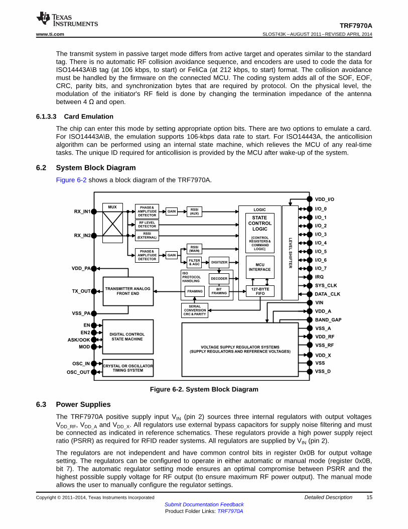
MUX
RX_IN1
RX_IN2
PHASE&
AMPLITUDE
DETECTOR
GAINRSSI
(AUX)LOGIC
LE
VE
LS
HIF
TE
RSTATE
CONTROL
LOGIC
[CONTROLREGISTERS&
COMMAND
LOGIC]
127-BYTEFIFO
MCU
INTERFACE
VDD_I/O
I/O_0
I/O_1
I/O_2
I/O_3
I/O_4
I/O_5
I/O_6
I/O_7
IRQ
SYS_CLK
DATA_CLK
ISO
PROTOCOL
HANDLINGDECODER
RSSI
(EXTERNAL)
PHASE&
AMPLITUDE
DETECTOR
GAIN
RSSI(MAIN)
FILTER& AGC
DIGITIZER
BIT
FRAMINGFRAMING
SERIAL
CONVERSION
CRC & PARITY
TRANSMITTER ANALOG
FRONT ENDTX_OUT
VDD_PA
VSS_PA
DIGITAL CONTROL
STATE MACHINE
CRYSTAL OR OSCILLATORTIMING SYSTEM
EN
EN2
ASK/OOK
MOD
OSC_IN
OSC_OUT
VOLTAGE SUPPLY REGULATOR SYSTEMS(SUPPLY REGULATORS AND REFERENCE VOLTAGES)
VSS_A
VSS_RF
VDD_RF
VDD_X
VSS_D
VSS
VIN
VDD_A
BAND_GAP
RF LEVELDETECTOR
TRF7970ASLOS743K –AUGUST 2011–REVISED APRIL 2014 www.ti.com
1.4 Functional Block DiagramFigure 1-1 shows the block diagram.
Figure 1-1. Block Diagram
2 Device Overview Copyright © 2011–2014, Texas Instruments IncorporatedSubmit Documentation FeedbackProduct Folder Links: TRF7970A

TRF7970Awww.ti.com SLOS743K –AUGUST 2011–REVISED APRIL 2014
Table of Contents1 Device Overview ......................................... 1 6.8 Transmitter – Digital Section ........................ 28
6.9 Transmitter – External Power Amplifier and1.1 Features .............................................. 1Subcarrier Detector ................................. 291.2 Applications........................................... 1
6.10 TRF7970A IC Communication Interface ............ 301.3 Description............................................ 16.11 Special Direct Mode for Improved MIFARE™1.4 Functional Block Diagram ............................ 2
Compatibility......................................... 482 Revision History ......................................... 4
6.12 NFC Modes.......................................... 483 Device Characteristics.................................. 5
6.13 Direct Commands from MCU to Reader ............ 514 Terminal Configuration and Functions.............. 6
6.14 Register Description................................. 554.1 Pin Assignments...................................... 6 7 Application Schematic and Layout4.2 Terminal Functions ................................... 7 Considerations.......................................... 75
5 Specifications ............................................ 9 7.1 TRF7970A Reader System Using ParallelMicrocontroller Interface............................. 755.1 Absolute Maximum Ratings .......................... 9
7.2 TRF7970A Reader System Using SPI With SS5.2 Recommended Operating Conditions ................ 9Mode ................................................ 765.3 Electrical Characteristics ............................ 10
7.3 Layout Considerations .............................. 775.4 Handling Ratings .................................... 117.4 Impedance Matching TX_Out (Pin 5) to 50 Ω ...... 775.5 Thermal Characteristics ............................. 117.5 Reader Antenna Design Guidelines ................ 795.6 Switching Characteristics ........................... 11
8 Device and Documentation Support ............... 806 Detailed Description ................................... 128.1 Documentation Support ............................. 806.1 Overview ............................................ 128.2 Community Resources .............................. 806.2 System Block Diagram.............................. 158.3 Trademarks.......................................... 806.3 Power Supplies...................................... 158.4 Electrostatic Discharge Caution..................... 806.4 Receiver – Analog Section .......................... 218.5 Glossary ............................................. 806.5 Receiver – Digital Section........................... 22
9 Mechanical Packaging and Orderable6.6 Oscillator Section ................................... 27Information .............................................. 80
6.7 Transmitter – Analog Section ....................... 289.1 Packaging Information .............................. 80
Copyright © 2011–2014, Texas Instruments Incorporated Table of Contents 3Submit Documentation FeedbackProduct Folder Links: TRF7970A

TRF7970ASLOS743K –AUGUST 2011–REVISED APRIL 2014 www.ti.com
2 Revision HistoryNOTE: Page numbers for previous revisions may differ from page numbers in the current version.
Changes from Revision J (February 2014) to Revision K Page
• Changed Figure 1-1 to show 127-byte FIFO...................................................................................... 2• Moved Section 3 ...................................................................................................................... 5• Changed title of Section 4 .......................................................................................................... 6• Changed title of Section 5 ........................................................................................................... 9• Added ASK/OOK and MOD to VIL and VIH ........................................................................................ 9• Moved Section 5.3 .................................................................................................................. 10• Changed VDD_A TYP value from 3.5 V to 3.4 V ................................................................................. 10• Moved Section 5.4 .................................................................................................................. 11• Added V(ESD) MIN values, test specifications, and notes....................................................................... 11• Changed title of Section 5.5 from Dissipation Ratings to Thermal Characteristics ......................................... 11• Moved Section 5.6 .................................................................................................................. 11• Changed title of Section 6.......................................................................................................... 12• Moved previous Section 3, Device Overview, to Section 6.1.................................................................. 12• Changed from "By default, the AGC is frozen after..." to "By default, the AGC window comparator is set after..." ... 21• Changed from "TX Pulse Length Control register (0x05)" to "TX Pulse Length Control register (0x06)" ............... 28• Changed from "18.8 s" to "18.8 µs" in the sentence that starts with "If the register contains all zeros..."............... 28• Changed Table 6-18 to match Table 6-43 ....................................................................................... 50• Changed command 0x18 to "Test internal RF" ................................................................................. 51• Changed command 0x19 to "Test external RF" ................................................................................ 51• Moved Section 6.14................................................................................................................. 55• Changed the sentence that starts "The AGC action is fast..." from "finishes after four subcarrier pulses" to
"finishes within eight subcarrier pulses" ......................................................................................... 64• Moved Section 7..................................................................................................................... 75• Deleted previous Section 10, System Design, and moved contents to Section 7.3 through Section 7.5 ............... 77• Removed references to figure numbers in Figure 7-3.......................................................................... 78
4 Revision History Copyright © 2011–2014, Texas Instruments IncorporatedSubmit Documentation FeedbackProduct Folder Links: TRF7970A

TRF7970Awww.ti.com SLOS743K –AUGUST 2011–REVISED APRIL 2014
3 Device CharacteristicsTable 3-1 shows the supported modes of operation for the TRF7970A device.
Table 3-1. Supported Modes of Operation
P2P Initiator or Reader/Writer Card Emulation P2P TargetBit rate Bit rate Bit rateTechnology Technology Technology(kbps) (kbps) (kbps)
106, 212, 424,NFC-A/B (ISO14443A/B) NFC-A/B 106 NFC-A 106848 (1)
NFC-F (JIS: X6319-4) 212, 424 N/A N/A NFC-F 212, 424NFC-V (ISO15693) 6.7, 26.7 N/A N/A N/A N/A
(1) 848 kbps only applies to reader/writer mode.
Copyright © 2011–2014, Texas Instruments Incorporated Device Characteristics 5Submit Documentation FeedbackProduct Folder Links: TRF7970A

VDD_A
VIN
VDD_RF
VDD_PA
TX_OUT
VSS_PA
VSS_RX
RX_IN1
I/0_7
RX
_IN
2
VS
S
BG
AS
K/O
OK
IRQ
MO
D
VS
S_
A
VD
D_
I/O
Pad
VD
D_
X
OS
C_
IN
OS
C_
OU
T
VS
S_
D
EN
SY
S_
CL
K
DA
TA
_C
LK
EN
2
1
2
3
4
5
6
7
8
24
23
22
21
20
19
18
17
9 10 11 12 13 14 15 16
32 31 30 29 28 27 26 25
I/0_6
I/0_5
I/0_4
I/0_3
I/0_2
I/0_1
I/0_0
TRF7970ASLOS743K –AUGUST 2011–REVISED APRIL 2014 www.ti.com
4 Terminal Configuration and Functions
4.1 Pin AssignmentsFigure 4-1 shows the pin assignments for the 32-pin RHB package.
Figure 4-1. 32-Pin RHB Package (Top View)
6 Terminal Configuration and Functions Copyright © 2011–2014, Texas Instruments IncorporatedSubmit Documentation FeedbackProduct Folder Links: TRF7970A

TRF7970Awww.ti.com SLOS743K –AUGUST 2011–REVISED APRIL 2014
4.2 Terminal FunctionsTable 4-1 describes the signals.
Table 4-1. Terminal FunctionsTERMINAL
TYPE (1) DESCRIPTIONNAME NO.
VDD_A 1 OUT Internal regulated supply (2.7 V to 3.4 V) for analog circuitryVIN 2 SUP External supply input to chip (2.7 V to 5.5 V)VDD_RF 3 OUT Internal regulated supply (2.7 V to 5 V), normally connected to VDD_PA (pin 4)VDD_PA 4 INP Supply for PA; normally connected externally to VDD_RF (pin 3)TX_OUT 5 OUT RF output (selectable output power, 100 mW or 200 mW, with VDD = 5 V)VSS_PA 6 SUP Negative supply for PA; normally connected to circuit groundVSS_RX 7 SUP Negative supply for RX inputs; normally connected to circuit groundRX_IN1 8 INP Main RX inputRX_IN2 9 INP Auxiliary RX inputVSS 10 SUP Chip substrate groundBAND_GAP 11 OUT Bandgap voltage (VBG = 1.6 V); internal analog voltage reference
Selection between ASK and OOK modulation (0 = ASK, 1 = OOK) for Direct Mode 0 or 1.ASK/OOK 12 BID
Can be configured as an output to provide the received analog signal output.IRQ 13 OUT Interrupt request
INP External data modulation input for Direct Mode 0 or 1MOD 14
OUT Subcarrier digital data output (see registers 0x1A and 0x1B)VSS_A 15 SUP Negative supply for internal analog circuits; connected to GNDVDD_I/O 16 INP Supply for I/O communications (1.8 V to VIN) level shifter. VIN should be never exceeded.I/O_0 17 BID I/O pin for parallel communicationI/O_1 18 BID I/O pin for parallel communication
I/O pin for parallel communicationI/O_2 19 BID
TX Enable (in Special Direct Mode)I/O pin for parallel communication
I/O_3 20 BIDTX Data (in Special Direct Mode)I/O pin for parallel communication
I/O_4 21 BIDSlave Select signal in SPI modeI/O pin for parallel communication
I/O_5 22 BIDData clock output in Direct Mode 1 and Special Direct ModeI/O pin for parallel communication
I/O_6 23 BID MISO for serial communication (SPI)Serial bit data output in Direct Mode 1 or subcarrier signal in Direct Mode 0I/O pin for parallel communication.
I/O_7 24 BIDMOSI for serial communication (SPI)Selection of power down mode. If EN2 is connected to VIN, then VDD_X is active during powerEN2 25 INP down mode 2 (for example, to supply the MCU).
DATA_CLK 26 INP Data Clock input for MCU communication (parallel and serial)
If EN = 1 (EN2 = don't care) the system clock for MCU is configured. Depending on the crystalthat is used, options are as follows (see register 0x09):
SYS_CLK 27 OUT 13.56-MHz crystal: Off, 3.39 MHz, 6.78 MHz, or 13.56 MHz27.12-MHz crystal: Off, 6.78 MHz, 13.56 MHz, or 27.12 MHz
If EN = 0 and EN2 = 1, then system clock is set to 60 kHzEN 28 INP Chip enable input (If EN = 0, then chip is in sleep or power-down mode).VSS_D 29 SUP Negative supply for internal digital circuits
(1) SUP = Supply, INP = Input, BID = Bidirectional, OUT = Output
Copyright © 2011–2014, Texas Instruments Incorporated Terminal Configuration and Functions 7Submit Documentation FeedbackProduct Folder Links: TRF7970A

TRF7970ASLOS743K –AUGUST 2011–REVISED APRIL 2014 www.ti.com
Table 4-1. Terminal Functions (continued)TERMINAL
TYPE (1) DESCRIPTIONNAME NO.
OSC_OUT 30 OUT Crystal or oscillator outputINP Crystal or oscillator input
OSC_IN 31OUT Crystal oscillator output
Internally regulated supply (2.7 V to 3.4 V) for digital circuit and external devices (for example,VDD_X 32 OUT MCU)Thermal Pad PAD SUP Chip substrate ground
8 Terminal Configuration and Functions Copyright © 2011–2014, Texas Instruments IncorporatedSubmit Documentation FeedbackProduct Folder Links: TRF7970A

TRF7970Awww.ti.com SLOS743K –AUGUST 2011–REVISED APRIL 2014
5 Specifications
5.1 Absolute Maximum Ratings (1) (2)
over operating free-air temperature range (unless otherwise noted)VIN Input voltage range -0.3 V to 6 VIIN Maximum current VIN 150 mA
Any condition 140°CTJ Maximum operating virtual junction temperature
Continuous operation, long-term reliability (3) 125°C
(1) Stresses beyond those listed under Absolute Maximum Ratings may cause permanent damage to the device. These are stress ratingsonly and functional operation of the device at these or any other conditions beyond those indicated under Operating Conditions are notimplied. Exposure to absolute-maximum-rated conditions for extended periods may affect device reliability.
(2) All voltage values are with respect to substrate ground terminal VSS.(3) The maximum junction temperature for continuous operation is limited by package constraints. Operation above this temperature may
result in reduced reliability or lifetime of the device.
5.2 Recommended Operating Conditionsover operating free-air temperature range (unless otherwise noted)
MIN TYP MAX UNITVIN Operating input voltage 2.7 5 5.5 VTA Operating ambient temperature -40 25 110 °CTJ Operating virtual junction temperature -40 25 125 °C
I/O lines, IRQ, SYS_CLK, DATA_CLK, 0.2 xVIL Input voltage - logic low VEN, EN2, ASK/OOK, MOD VDD_I/O
I/O lines, IRQ, SYS_CLK, DATA_CLK, 0.8 xVIH Input voltage threshold, logic high VEN, EN2, ASK/OOK, MOD VDD_I/O
Copyright © 2011–2014, Texas Instruments Incorporated Specifications 9Submit Documentation FeedbackProduct Folder Links: TRF7970A

TRF7970ASLOS743K –AUGUST 2011–REVISED APRIL 2014 www.ti.com
5.3 Electrical CharacteristicsTYP operating conditions are TA = 25°C, VIN = 5 V, full-power mode (unless otherwise noted)MIN and MAX operating conditions are over recommended ranges of supply voltage and operating free-air temperature(unless otherwise noted)
PARAMETER TEST CONDITIONS MIN TYP MAX UNITAll building blocks disabled, including supply-
IPD1 Supply current in Power Down Mode 1 voltage regulators; measured after 500-ms 0.5 5 µAsettling time (EN = 0, EN2 = 0)The SYS_CLK generator and VDD_X remainSupply current in Power Down Mode 2IPD2 active to support external circuitry; measured 120 200 µA(Sleep Mode) after 100-ms settling time (EN = 0, EN2 = 1)Oscillator running, supply-voltage regulators inISTBY Supply current in stand-by mode 1.9 3.5 mAlow-consumption mode (EN = 1, EN2 = x)
Supply current without antenna driver Oscillator, regulators, RX and AGC active, TXION1 10.5 14 mAcurrent is offOscillator, regulators, RX and AGC and TXION2 Supply current – TX (half power) 70 78 mAactive, POUT = 100 mWOscillator, regulators, RX and AGC and TXION3 Supply current – TX (full power) 130 150 mAactive, POUT = 200 mW
VPOR Power-on reset voltage Input voltage at VIN 1.4 2 2.6 VVBG Bandgap voltage (pin 11) Internal analog reference voltage 1.5 1.6 1.7 V
Regulated output voltage for analogVDD_A VIN = 5 V 3.1 3.4 3.8 Vcircuitry (pin 1)VDD_X Regulated supply for external circuitry Output voltage pin 32, VIN = 5 V 3.1 3.4 3.8 VIVDD_Xmax Maximum output current of VDD_X Output current pin 32, VIN = 5 V 20 mA
Half-power mode, VIN = 2.7 V to 5.5 V 8 12RRFOUT Antenna driver output resistance (1) Ω
Full-power mode, VIN = 2.7 V to 5.5 V 4 6RRFIN RX_IN1 and RX_IN2 input resistance 4 10 20 kΩ
Maximum RF input voltage at RX_IN1 andVRF_INmax VRF_INmax should not exceed VIN 3.5 VppRX_IN2fSUBCARRIER= 424 kHz 1.4 2.5Minimum RF input voltage at RX_IN1 andVRF_INmin mVppRX_IN2 (input sensitivity) (2) fSUBCARRIER = 848 kHz 2.1 3
fSYS_CLK SYS_CLK frequency In power mode 2, EN = 0, EN2 = 1 25 60 120 kHzfC Carrier frequency Defined by external crystal 13.56 MHz
Time until oscillator stable bit is set (registertCRYSTAL Crystal run-in time 3 ms0x0F) (3)
Depends on capacitive load on the I/O lines,fD_CLKmax Maximum DATA_CLK frequency (4) 2 8 10 MHzrecommendation is 2 MHz (4)
ROUT Output resistance I/O_0 to I/O_7 500 800 ΩRSYS_CLK Output resistance RSYS_CLK 200 400 Ω
(1) Antenna driver output resistance(2) Measured with subcarrier signal at RX_IN1 or RX_IN2 and measured the digital output at MOD pin with register 0x1A bit 6 = 1.(3) Depends on the crystal parameters and components(4) Recommended DATA_CLK speed is 2 MHz. Higher data clock depends on the capacitive load. Maximum SPI clock speed should not
exceed 10 MHz. This clock speed is acceptable only when external capacitive load is less than 30 pF. MISO driver has a typical outputresistance of 400 Ω (12-ns time constant when 30-pF load used).
10 Specifications Copyright © 2011–2014, Texas Instruments IncorporatedSubmit Documentation FeedbackProduct Folder Links: TRF7970A

TRF7970Awww.ti.com SLOS743K –AUGUST 2011–REVISED APRIL 2014
5.4 Handling RatingsMIN MAX UNIT
TSTG Storage temperature range -55 150 °CV(ESD) Electrostatic discharge Human-Body Model (HBM), per ANSI/ESDA/JEDEC JS-001, all pins (1) -2 2 kV
Charged-Device Model (CDM), per JEDEC specification JESD22-C101, -500 500 Vall pins (2)
Machine Model (MM) -200 200 V
(1) JEDEC document JEP155 states that 500-V HBM allows safe manufacturing with a standard ESD control process. Pins listed as 2 kVmay actually have higher performance.
(2) JEDEC document JEP157 states that 250-V CDM allows safe manufacturing with a standard ESD control process. Pins listed as 500 Vmay actually have higher performance.
5.5 Thermal CharacteristicsPOWER RATING (2)
PACKAGE θJC θJA(1)
TA ≤ 25°C TA ≤ 85°CRHB (32 pin) 31°C/W 36.4°C/W 2.7 W 1.1 W
(1) This data was taken using the JEDEC standard high-K test PCB.(2) Power rating is determined with a junction temperature of 125°C. This is the point where distortion starts to increase substantially.
Thermal management of the final PCB should strive to keep the junction temperature at or below 125°C for best performance and long-term reliability.
5.6 Switching CharacteristicsTYP operating conditions are TA = 25°C, VIN = 5 V, full-power mode (unless otherwise noted)MIN and MAX operating conditions are over recommended ranges of supply voltage and operating free-air temperature(unless otherwise noted)
PARAMETER TEST CONDITIONS MIN TYP MAX UNITDATA_CLK time high or low, one half oftLO/HI Depends on capacitive load on the I/O lines (1) 250 62.5 50 nsDATA_CLK at 50% duty cycleSlave select lead time, slave select low totSTE,LEAD 200 nsclockSlave select lag time, last clock to slavetSTE,LAG 200 nsselect highSlave select disable time, slave select
tSTE,DIS rising edge to next slave select falling 300 nsedge
tSU,SI MOSI input data setup time 15 nstHD,SI MOSI input data hold time 15 nstSU,SO MISO input data setup time 15 nstHD,SO MISO input data hold time 15 nstVALID,SO MISO output data valid time DATA_CLK edge to MISO valid, CL ≤ 30 pF 30 50 75 ns
(1) Recommended DATA_CLK speed is 2 MHz. Higher data clock depends on the capacitive load. Maximum SPI clock speed should notexceed 10 MHz. This clock speed is acceptable only when external capacitive load is less than 30 pF. MISO driver has a typical outputresistance of 400 Ω (12-ns time constant when 30-pF load used).
Copyright © 2011–2014, Texas Instruments Incorporated Specifications 11Submit Documentation FeedbackProduct Folder Links: TRF7970A

TRF7970A MCU(MSP430/ARM)
Matching
VDD_X VDD_I/O
TX_OUT
RX_IN 1
RX_IN2 VSS VIN
Parallelor SPI
Supply: 2.7 V – 5.5 V
VDD
VDD
Crystal13.56 MHz
XIN
TRF7970ASLOS743K –AUGUST 2011–REVISED APRIL 2014 www.ti.com
6 Detailed Description
6.1 Overview
6.1.1 RFID and NFC Operation – Reader and WriterThe TRF7970A is a high performance 13.56-MHz HF RFID and NFC Transceiver IC composed of anintegrated analog front end (AFE) and a built-in data framing engine for ISO15693, ISO14443A/B, andFeliCa. This includes data rates up to 848 kbps for ISO14443 with all framing and synchronization taskson board (in default mode). The TRF7970A also supports NFC Tag Type 1, 2, 3, and 4 operations. Thisarchitecture enables the customer to build a complete cost-effective yet high-performance multi-protocol13.56-MHz RFID and NFC system together with a low-cost microcontroller.
Other standards and even custom protocols can be implemented by using either of the Direct Modes thatthe device offers. These Direct Modes (0 and 1) allow the user to fully control the analog front end (AFE)and also gain access to the raw subcarrier data or the unframed but already ISO formatted data and theassociated (extracted) clock signal.
The receiver system has a dual input receiver architecture. The receivers also include various automaticand manual gain control options. The received input bandwidth can be selected to cover a broad range ofinput subcarrier signal options.
The received signal strength from transponders, ambient sources, or internal levels is available throughthe RSSI register. The receiver output is selectable among a digitized subcarrier signal and any of theintegrated subcarrier decoders. The selected subcarrier decoder delivers the data bit stream and the dataclock as outputs.
The TRF7970A also includes a receiver framing engine. This receiver framing engine performs the CRCor parity check, removes the EOF and SOF settings, and organizes the data in bytes for ISO14443A/B,ISO15693, and FeliCa protocols. Framed data is then accessible to the microcontroller (MCU) through a127-byte FIFO register.
Figure 6-1. Application Block Diagram
A parallel or serial interface (SPI) can be used for the communication between the MCU and theTRF7970A reader. When the built-in hardware encoders and decoders are used, transmit and receivefunctions use a 127-byte FIFO register. For direct transmit or receive functions, the encoders anddecoders can be bypassed so that the MCU can process the data in real time. The TRF7970A supportsdata communication voltage levels from 1.8 V to 5.5 V for the MCU I/O interface. The transmitter hasselectable output-power levels of 100 mW (+20 dBm) or 200 mW (+23 dBm) equivalent into a 50-Ω loadwhen using a 5-V supply.
12 Detailed Description Copyright © 2011–2014, Texas Instruments IncorporatedSubmit Documentation FeedbackProduct Folder Links: TRF7970A

TRF7970Awww.ti.com SLOS743K –AUGUST 2011–REVISED APRIL 2014
The transmitter supports OOK and ASK modulation with selectable modulation depth. The TRF7970A alsoincludes a data transmission engine that comprises low-level encoding for ISO15693, ISO14443A/B andFeliCa. Included with the transmit data coding is the automatic generation of Start Of Frame (SOF), EndOf Frame (EOF), Cyclic Redundancy Check (CRC), or parity bits.
Several integrated voltage regulators ensure a proper power-supply noise rejection for the completereader system. The built-in programmable auxiliary voltage regulator VDD_X (pin 32), is able to deliver up to20 mA to supply a microcontroller and additional external circuits within the reader system.
6.1.2 NFC Device Operation – InitiatorThe desired system of operation (bit rate) is achieved by selecting the option bits in control registers in thesame way as for RFID reader operation. Also the communication to external MCU and data exchange isidentical.
The transmitting system comprises an RF level detector (programmable level) which is used for initial (orresponse) RF collision avoidance. The RF collision avoidance sequence is started by sending a directcommand. If successful, the NFC initiator can send the data or commands, the MCU has loaded in theFIFO register. The coding of this data is done by hardware coders either in ISO14443A/B format or inFeliCa format. The coders also provide CRC and parity bits (if required) and automatically add preambles,SOF, EOF, and synchronization bytes as defined by selected protocol.
The receiver system offers same analog features (AGC, AM/PM, bandwidth selection, etc.) as describedpreviously in RFID and NFC reader and writer description. The system comprises integrated decoders forpassive targets (ISO14443A/B tag or FeliCa) or active targets (ISO14443A/B reader or FeliCa). For all thisoptions, the system also supports framing including CRC and parity check and removal of SOF, EOF, andsynchronization bytes as specified by the selected protocol.
6.1.3 NFC Device Operation – TargetThe desired system of operation (bit rate) is achieved by selecting the option bits in control registers in thesame way as for RFID reader or NFC initiator operation. Also the communication to external MCU anddata exchange is identical.
The activation of NFC target is done when a sufficient RF field level is detected on the antenna. The levelneeded for wake-up is selectable and is stored in non-volatile register.
When the activation occurs, the system performs automatic power-up and waits for the first command tobe received. Based on this command, the system knows if it should operate as passive or active targetand at what bit rate. After activation, the receiver system offers the same analog features (for example,AGC, AM/PM, and bandwidth selection) as in the case of an RFID reader.
When used as the NFC target, the chip is typically in a power down or standby mode. If EN2 = H, the chipkeeps the supply system on. If EN2 = L and EN = L, the chip is in complete power down. To operate asNFC target or Tag emulator, the MCU must load a value different from zero (0) in Target Detection Levelregister (B0-B2) to enable the RF measurement system (supplied by VEXT, so it can operate also duringcomplete power down and consumes only 3.5 µA). The RF measurement constantly monitors the RFsignal on the antenna input. When the RF level on the antenna input exceeds the level defined in the inTarget Detection Level register, the chip is automatically activated (EN is internally forced high).
When the voltage supply system and the oscillator are started and are stable, osc_ok goes high (B6 ofRSSI Level and Oscillator Status register) and IRQ is sent with bit B2 = 1 of IRQ register (field change).Bit B7 NFC Target Protocol in register directly displays the status of RF level detection (running constantlyalso during normal operation). This informs the MCU that the chip should start operation as NFC TARGETdevice. When the first command from the INITIATOR is received another IRQ sent with B6 (RX start) set
Copyright © 2011–2014, Texas Instruments Incorporated Detailed Description 13Submit Documentation FeedbackProduct Folder Links: TRF7970A

TRF7970ASLOS743K –AUGUST 2011–REVISED APRIL 2014 www.ti.com
in IRQ register. The MCU must set EN = H (confirm the power-up) in the time between the two IRQs,because the internal power-up ends after the second IRQ. The type and coding of the first initiator (orreader in the case of a tag emulator) command defines the communication protocol type that the targetmust use. Therefore, the communication protocol type is available in the NFC Target Protocol registerimmediately after receiving the first command.
Based on the first command from the INITIATOR, the following actions are taken:• If the first command is SENS_REQ or ALL_REQ the TARGET must enter the SDD protocol for 106-
kbps passive communication to begin; afterward, the baud rate can be changed to 212 kbps or 424kbps, according to the system requirements. If bit B5 in the NFC Target Detection Level register is notset, the MCU handles the SDD and the command received is send to FIFO. If the RF field is turned off(B7 in NFC Target Protocol register is low) at any time, the system sends an IRQ to the MCU with bitB2 (RF field change) in the IRQ register set high. This informs the MCU that the procedure wasaborted and the system must be reset. The clock extractor is automatically activated in this mode.
• If the command is SENS_REQ or ALL_REQ and the card emulation bit in ISO Control register is set,the system emulates an ISO14443A/B tag. The procedure does not differ from the one previouslydescribed for the case of a passive target at 106 kbps. The clock extractor is automatically activated inthis mode. To emulate a FeliCa card, the ISO Control register must be set for passive target mode ateither 212 kbps or 424 kbps.
• If the first command is a POLLING request, the system becomes the TARGET in passivecommunication using 212 kbps or 424 kbps. The SDD is relatively simple and is handled by the MCUdirectly. The POLLING response is sent in one of the slots automatically calculated by the MCU (firstslot starts 2.416 ms after end of command, and slots follow in 1.208 ms).
• If the first command is ATR_REQ, the system operates as an active TARGET using the samecommunication speed and bit coding as used by the INITIATOR. Again, all of the replies are handledby MCU. The chip is only required to time the response collision avoidance, which is done on directcommand from MCU. When the RF field is switched on and the minimum wait time is elapsed, the chipsends an IRQ with B1 (RF collision avoidance finished) set high. This signals the MCU that it can sendthe reply.
• If the first command is coded as ISO14443B and the Tag emulation bit is set in the ISO Controlregister, the system enters ISO14443B emulation mode. The anticollision must be handled by theMCU, and the chip provides all physical level coding, decoding, and framing for this protocol.
6.1.3.1 Active Target
If the first command received by the RF interface defines the system as an active target, then the receiverselects the appropriate data decoders (ISO14443A\B reader or FeliCa) and framing option. Only the raw(decoded) data is forwarded to the MCU through the FIFO. SOF, EOF, preamble, sync bytes, CRC, andparity bytes are checked by the framer and discarded.
The transmitting system includes an RF level detector (programmable level) that is used for RF collisionavoidance. The RF collision avoidance sequence is started by sending a direct command. If successful,the NFC initiator can send the data that the MCU has loaded in the FIFO register. The coding of this datais done by hardware coders either in ISO14443A format (106-kbps system) or in FeliCa format for (212-kbps and 424-kbps systems). The coders also provide CRC and parity bits (if required) and automaticallyadd preambles, SOF, EOF, and synchronization bytes as defined by selected protocol.
6.1.3.2 Passive Target
If the first command received by the RF interface defines the system as a passive target, then the receiverselects the appropriate data decoders (ISO14443A\B reader or FeliCa) and framing option. Again, only theraw (decoded) data is forwarded to the MCU through the FIFO; SOF, EOF, preamble, sync bytes, CRC,and parity bytes are checked by the framer and discarded. The receiver works same as in the case of anactive target.
14 Detailed Description Copyright © 2011–2014, Texas Instruments IncorporatedSubmit Documentation FeedbackProduct Folder Links: TRF7970A
MUX
RX_IN1
RX_IN2
PHASE&
AMPLITUDE
DETECTOR
GAINRSSI
(AUX)LOGIC
LE
VE
LS
HIF
TE
R
STATE
CONTROL
LOGIC
[CONTROLREGISTERS&
COMMAND
LOGIC]
127-BYTEFIFO
MCU
INTERFACE
VDD_I/O
I/O_0
I/O_1
I/O_2
I/O_3
I/O_4
I/O_5
I/O_6
I/O_7
IRQ
SYS_CLK
DATA_CLK
ISO
PROTOCOL
HANDLINGDECODER
RSSI
(EXTERNAL)
PHASE&
AMPLITUDE
DETECTOR
GAIN
RSSI(MAIN)
FILTER& AGC
DIGITIZER
BIT
FRAMINGFRAMING
SERIAL
CONVERSION
CRC & PARITY
TRANSMITTER ANALOG
FRONT ENDTX_OUT
VDD_PA
VSS_PA
DIGITAL CONTROL
STATE MACHINE
CRYSTAL OR OSCILLATORTIMING SYSTEM
EN
EN2
ASK/OOK
MOD
OSC_IN
OSC_OUT
VOLTAGE SUPPLY REGULATOR SYSTEMS(SUPPLY REGULATORS AND REFERENCE VOLTAGES)
VSS_A
VSS_RF
VDD_RF
VDD_X
VSS_D
VSS
VIN
VDD_A
BAND_GAP
RF LEVELDETECTOR
TRF7970Awww.ti.com SLOS743K –AUGUST 2011–REVISED APRIL 2014
The transmit system in passive target mode differs from active target and operates similar to the standardtag. There is no automatic RF collision avoidance sequence, and encoders are used to code the data forISO14443A\B tag (at 106 kbps, to start) or FeliCa (at 212 kbps, to start) format. The collision avoidancemust be handled by the firmware on the connected MCU. The coding system adds all of the SOF, EOF,CRC, parity bits, and synchronization bytes that are required by protocol. On the physical level, themodulation of the initiator's RF field is done by changing the termination impedance of the antennabetween 4 Ω and open.
6.1.3.3 Card Emulation
The chip can enter this mode by setting appropriate option bits. There are two options to emulate a card.For ISO14443A\B, the emulation supports 106-kbps data rate to start. For ISO14443A, the anticollisionalgorithm can be performed using an internal state machine, which relieves the MCU of any real-timetasks. The unique ID required for anticollision is provided by the MCU after wake-up of the system.
6.2 System Block DiagramFigure 6-2 shows a block diagram of the TRF7970A.
Figure 6-2. System Block Diagram
6.3 Power SuppliesThe TRF7970A positive supply input VIN (pin 2) sources three internal regulators with output voltagesVDD_RF, VDD_A and VDD_X. All regulators use external bypass capacitors for supply noise filtering and mustbe connected as indicated in reference schematics. These regulators provide a high power supply rejectratio (PSRR) as required for RFID reader systems. All regulators are supplied by VIN (pin 2).
The regulators are not independent and have common control bits in register 0x0B for output voltagesetting. The regulators can be configured to operate in either automatic or manual mode (register 0x0B,bit 7). The automatic regulator setting mode ensures an optimal compromise between PSRR and thehighest possible supply voltage for RF output (to ensure maximum RF power output). The manual modeallows the user to manually configure the regulator settings.
Copyright © 2011–2014, Texas Instruments Incorporated Detailed Description 15Submit Documentation FeedbackProduct Folder Links: TRF7970A
TRF7970ASLOS743K –AUGUST 2011–REVISED APRIL 2014 www.ti.com
6.3.1 Supply ArrangementsRegulator Supply Input: VIN
The positive supply at VIN (pin 2) has an input voltage range of 2.7 V to 5.5 V. VIN provides the supplyinput sources for three internal regulators with the output voltages VDD_RF, VDD_A, and VDD_X. Externalbypass capacitors for supply noise filtering must be used (per reference schematics).
NOTEVIN must be the highest voltage supplied to the TRF7970A.
RF Power Amplifier Regulator: VDD_RF
The VDD_RF (pin 3) regulator is supplying the RF power amplifier. The voltage regulator can be set foreither 5-V or 3-V operation. External bypass capacitors for supply noise filtering must be used (perreference schematics). When configured for 5-V manual-operation, the VDD_RF output voltage can be setfrom 4.3 V to 5 V in 100-mV steps. In 3-V manual-operation, the output can be programmed from 2.7 V to3.4 V in 100-mV steps. The maximum output current capability for 5-V operation is 150 mA and for 3-Voperation is 100 mA.
Analog Supply Regulator: VDD_A
Regulator VDD_A (pin 1) supplies the analog circuits of the device. The output voltage setting depends onthe input voltage and can be set for 5-V and 3-V operation. When configured for 5-V manual-operation,the output voltage is fixed at 3.4 V. External bypass capacitors for supply noise filtering must be used (perreference schematics). When configured for 3-V manual-operation, the VDD_A output can be set from 2.7 Vto 3.4 V in 100-mV steps (see Table 6-2).
Note: the configuration of VDD_A and VDD_X regulators are not independent from each other. The VDD_Aoutput current should not exceed 20 mA.
Digital Supply Regulator: VDD_X
The digital supply regulator VDD_X (pin 32) provides the power for the internal digital building blocks andcan also be used to supply external electronics within the reader system. When configured for 3-Voperation, the output voltage can be set from 2.7 to 3.4 V in 100-mV steps. External bypass capacitors forsupply noise filtering must be used (per reference schematics).
Note: the configuration of the VDD_A and VDD_X regulators are not independent from each other. The VDD_Xoutput current should not exceed 20 mA.
The RF power amplifier regulator (VDD_RF), analog supply regulator (VDD_A) and digital supply regulator(VDD_X) can be configured to operate in either automatic or manual mode described in Section 6.3.2. Theautomatic regulator setting mode ensures an optimal compromise between PSRR and the highestpossible supply voltage to ensure maximum RF power output.
By default, the regulators are set in automatic regulator setting mode. In this mode, the regulators areautomatically set every time the system is activated by setting EN input High or each time the automaticregulator setting bit, B7 in register 0x0B is set to a 1. The action is started on the 0 to 1 transition. Thismeans that, if the user wants to re-run the automatic setting from a state in which the automatic setting bitis already high, the automatic setting bit (B7 in register 0x0B) should be changed: 1-0-1.
By default, the regulator setting algorithm sets the regulator outputs to a "Delta Voltage" of 250 mV belowVIN, but not higher than 5 V for VDD_RF and 3.4 V for VDD_A and VDD_A. The "Delta Voltage" in automaticregulator mode can be increased up to 400 mV (for details, see bits B0 to B2 in register 0x0B).
16 Detailed Description Copyright © 2011–2014, Texas Instruments IncorporatedSubmit Documentation FeedbackProduct Folder Links: TRF7970A

TRF7970Awww.ti.com SLOS743K –AUGUST 2011–REVISED APRIL 2014
Power Amplifier Supply: VDD_PA
The power amplifier of the TRF7970A is supplied through VDD_PA(pin 4). The positive supply pin for the RFpower amplifier is externally connected to the regulator output VDD_RF (pin 3).
I/O Level Shifter Supply: VDD_I/O
The TRF7970A has a separate supply input VDD_I/O (pin 16) for the built-in I/O level shifter. The supportedinput voltage ranges from 1.8 V to VIN, not exceeding 5.5 V. Pin 16 is used to supply the I/O interface pins(I/O_0 to I/O_7), IRQ, SYS_CLK, and DATA_CLK pins of the reader. In typical applications, VDD_I/O isdirectly connected to VDD_X, while VDD_X also supplies the MCU. This ensures that the I/O signal levels ofthe MCU match the logic levels of the TRF7970A.
Negative Supply Connections: VSS, VSS_TX, VSS_RX, VSS_A, VSS_PA
The negative supply connections VSS_X of each functional block are all externally connected to GND.
The substrate connection is VSS (pin 10), the analog negative supply is VSS_A (pin 15), the logic negativesupply is VSS_D (pin 29), the RF output stage negative supply is VSS_PA (pin 6), and the negative supply forthe RF receiver VSS_RX (pin 7).
Copyright © 2011–2014, Texas Instruments Incorporated Detailed Description 17Submit Documentation FeedbackProduct Folder Links: TRF7970A

TRF7970ASLOS743K –AUGUST 2011–REVISED APRIL 2014 www.ti.com
6.3.2 Supply Regulator SettingsThe input supply voltage mode of the reader needs to be selected. This is done in the Chip Status Controlregister (0x00). Bit 0 in register 0x00 selects between 5-V or 3-V input supply voltage. The defaultconfiguration is 5 V, which reflects an operating supply voltage range of 4.3 V to 5.5 V. If the supplyvoltage is below 4.3 V, the 3-V configuration should be used.
The various regulators can be configured to operate in automatic or manual mode. This is done in theRegulator and I/O Control register (0x0B) as shown in Table 6-1 and Table 6-2.
Table 6-1. Supply Regulator Setting: 5-V System
Register Option Bits Setting in Regulator Control Register (1)
Address CommentsB7 B6 B5 B4 B3 B2 B1 B0(hex)
Automatic Mode (default)0B 1 x x x x x 0 0 Automatic regulator setting 400-mV difference
Manual Mode0B 0 x x x x 1 1 1 VDD_RF = 5 V, VDD_A = 3.4 V, VDD_X = 3.4 V0B 0 x x x x 1 1 0 VDD_RF = 4.9 V, VDD_A = 3.4 V, VDD_X = 3.4 V0B 0 x x x x 1 0 1 VDD_RF = 4.8 V, VDD_A = 3.4 V, VDD_X = 3.4 V0B 0 x x x x 1 0 0 VDD_RF = 4.7 V, VDD_A = 3.4 V, VDD_X = 3.4 V0B 0 x x x x 0 1 1 VDD_RF = 4.6 V, VDD_A = 3.4 V, VDD_X = 3.4 V0B 0 x x x x 0 1 0 VDD_RF = 4.5 V, VDD_A = 3.4 V, VDD_X = 3.4 V0B 0 x x x x 0 0 1 VDD_RF = 4.4 V, VDD_A = 3.4 V, VDD_X = 3.4 V0B 0 x x x x 0 0 0 VDD_RF = 4.3 V, VDD_A = 3.4 V, VDD_X = 3.4 V
(1) x = Don't care
Table 6-2. Supply Regulator Setting: 3-V System
Register Option Bits Setting in Regulator Control Register (1)
Address CommentsB7 B6 B5 B4 B3 B2 B1 B0(hex)
Automatic Mode (default)0B 1 x x x x x 0 0 Automatic regulator setting 400-mV difference
Manual Mode0B 0 x x x x 1 1 1 VDD_RF = 3.4 V, VDD_A = 3.4 V, VDD_X = 3.4 V0B 0 x x x x 1 1 0 VDD_RF = 3.3 V, VDD_A = 3.3 V, VDD_X = 3.3 V0B 0 x x x x 1 0 1 VDD_RF = 3.2 V, VDD_A = 3.2 V, VDD_X = 3.2 V0B 0 x x x x 1 0 0 VDD_RF = 3.1 V, VDD_A = 3.1 V, VDD_X = 3.1 V0B 0 x x x x 0 1 1 VDD_RF = 3.0 V, VDD_A = 3.0 V, VDD_X = 3.0 V0B 0 x x x x 0 1 0 VDD_RF = 2.9 V, VDD_A = 2.9 V, VDD_X = 2.9 V0B 0 x x x x 0 0 1 VDD_RF = 2.8 V, VDD_A = 2.8 V, VDD_X = 2.8 V0B 0 x x x x 0 0 0 VDD_RF = 2.7 V, VDD_A = 2.7 V, VDD_X = 2.7 V
(1) x = Don't care
The regulator configuration function adjusts the regulator outputs by default to 400 mV below VIN level, butnot higher than 5 V for VDD_RF, 3.4 V for VDD_A and VDD_X. This ensures the highest possible supplyvoltage for the RF output stage while maintaining an adequate PSRR (power supply rejection ratio).
18 Detailed Description Copyright © 2011–2014, Texas Instruments IncorporatedSubmit Documentation FeedbackProduct Folder Links: TRF7970A

TRF7970Awww.ti.com SLOS743K –AUGUST 2011–REVISED APRIL 2014
6.3.3 Power ModesThe chip has several power states, which are controlled by two input pins (EN and EN2) and several bitsin the chip status control register (0x00) (see Table 6-3 and Table 6-4).
Table 6-3. 3.3-V Operation Power Modes (1)
Chip Regulator TypicalStatus SYS_CLK TypicalControl SYS_CLK PowerMode EN2 EN Control Transmitter Receiver (13.56 VDD_X CurrentRegister (60 kHz) OutRegister MHz) (mA)(0x0B) (dBm)(0x00)
Power Down 0 0 XX XX OFF OFF OFF OFF OFF <0.001 -
Sleep Mode 1 0 XX XX OFF OFF OFF ON ON 0.120 -
Standby Mode at X 1 80 00 OFF OFF ON X ON 2 -+3.3 VDC
Mode 1 at +3.3 VDC X 1 00 00 OFF OFF ON X ON 3 -
Mode 2 at +3.3 VDC X 1 02 00 OFF ON ON X ON 9 -
Mode 3 (Half Power) at X 1 30 07 ON ON ON X ON 53 14.5+3.3 VDC
Mode 4 (Full Power) at X 1 20 07 ON ON ON X ON 67 17+3.3 VDC
(1) X = Don't care
Table 6-4. 5-V Operation Power Modes (1)
Chip Regulator TypicalStatus SYS_CLK TypicalControl SYS_CLK PowerMode EN2 EN Control Transmitter Receiver (13.56 VDD_X CurrentRegister (60 kHz) OutRegister MHz) (mA)(0x0B) (dBm)(0x00)
Power Down 0 0 XX XX OFF OFF OFF OFF OFF <0.001 -
Sleep Mode 1 0 XX XX OFF OFF OFF ON ON 0.120 -
Standby Mode at X 1 81 07 OFF OFF ON X ON 3 -+5 VDC
Mode 1 at +5 VDC X 1 01 07 OFF OFF ON X ON 5 -
Mode 2 at +5 VDC X 1 03 07 OFF ON ON X ON 10.5 -
Mode 3 (Half Power) at X 1 31 07 ON ON ON X ON 70 20+5 VDC
Mode 4 (Full Power) at X 1 21 07 ON ON ON X ON 130 23+5 VDC
(1) X = Don't care
Table 6-3 and Table 6-4 show the configuration for the different power modes when using a 3.3-V or 5-Vsystem supply, respectively. The main reader enable signal is pin EN. When EN is set high, all of thereader regulators are enabled, the 13.56-MHz oscillator is running and the SYS_CLK (output clock forexternal micro controller) is also available.
The input pin EN2 has two functions:• A direct connection from EN2 to VIN to ensure the availability of the regulated supply VDD_X and an
auxiliary clock signal (60 kHz, SYS_CLK) for an external MCU. This mode (EN = 0, EN2 = 1) isintended for systems in which the MCU is also being supplied by the reader supply regulator (VDD_X)and the MCU clock is supplied by the SYS_CLK output of the reader. This allows the MCU supply andclock to be available during sleep mode.
• EN2 enables the start-up of the reader system from complete power down (EN = 0, EN2 = 0). In thiscase the EN input is being controlled by the MCU (or other system device) that is without supplyvoltage during complete power down (thus unable to control the EN input). A rising edge applied to theEN2 input (which has an approximately 1-V threshold level) starts the reader supply system and 13.56-MHz oscillator (identical to condition EN = 1).
Copyright © 2011–2014, Texas Instruments Incorporated Detailed Description 19Submit Documentation FeedbackProduct Folder Links: TRF7970A

VIN
EN2
EN
5 ms
6 ms
VIN
SS
EN2
EN
2 ms
5 ms
6 ms
TRF7970ASLOS743K –AUGUST 2011–REVISED APRIL 2014 www.ti.com
When user MCU is controlling EN and EN2, a delay of 1 ms between EN and EN2 must be used. If theMCU controls only EN, EN2 is recommended to be connected to either VIN or GND, depending on theapplication MCU requirements for VDD_X and SYS_CLK.
Figure 6-3. Nominal Start-Up Sequence Using SPI With SS (MCU Controls EN2)
Figure 6-4. Nominal Start-Up Sequence Using Parallel (MCU Controls EN2)
This start-up mode lasts until all of the regulators have settled and the 13.56-MHz oscillator has stabilized.If the EN input is set high (EN = 1) by the MCU (or other system device), the reader stays active. If the ENinput is not set high (EN = 0) within 100 µs after the SYS_CLK output is switched from auxiliary clock (60kHz) to high-frequency clock (derived from the crystal oscillator), the reader system returns to completePower-Down Mode 1. This option can be used to wake-up the reader system from complete Power Down(PD Mode 1) by using a pushbutton switch or by sending a single pulse.
After the reader EN line is high, the other power modes are selected by control bits within the chip statuscontrol register (0x00). The power mode options and states are listed in Table 6-3.
When EN is set high (or on rising edge of EN2 and then confirmed by EN = 1) the supply regulators areactivated and the 13.56-MHz oscillator started. When the supplies are settled and the oscillator frequencyis stable, the SYS_CLK output is switched from the auxiliary frequency of 60 kHz to the 13.56-MHzfrequency derived from the crystal oscillator. At this point, the reader is ready to communicate and performthe required tasks. The MCU can then program the chip status control register 0x00 and select theoperation mode by programming the additional registers.• Stand-by Mode (bit 7 = 1 of register 0x00), the reader is capable of recovering to full operation in
100 µs.• Mode 1 (active mode with RF output disabled, bit 5 = 0 and bit 1 = 0 of register 0x00) is a low power
mode which allows the reader to recover to full operation within 25 µs.• Mode 2 (active mode with only the RF receiver active, bit 1 = 1 of register 0x00) can be used to
measure the external RF field (as described in RSSI measurements paragraph) if reader-to-readeranticollision is implemented.
• Modes 3 and 4 (active modes with the entire RF section active, bit 5 = 1 of register 0x00) are thenormal modes used for normal transmit and receive operations.
20 Detailed Description Copyright © 2011–2014, Texas Instruments IncorporatedSubmit Documentation FeedbackProduct Folder Links: TRF7970A

TRF7970Awww.ti.com SLOS743K –AUGUST 2011–REVISED APRIL 2014
6.4 Receiver – Analog Section
6.4.1 Main and Auxiliary ReceiversThe TRF7970A has two receiver inputs: RX_IN1 (pin 8) and RX_IN2 (pin 9). Each of the input isconnected to an external capacitive voltage divider to ensure that the modulated signal from the tag isavailable on at least one of the two inputs. This architecture eliminates any possible communication holesthat may occur from the tag to the reader.
The two RX inputs (RX_IN1 and RX_IN2) are multiplexed into two receivers - the main receiver and theauxiliary receiver. Only the main receiver is used for reception, the auxiliary receiver is used for signalquality monitoring. Receiver input multiplexing is controlled by bit B3 in the Chip Status Control register(address 0x00).
After startup, RX_IN1 is multiplexed to the main receiver which is composed of an RF envelope detection,first gain and band-pass filtering stage, second gain and filtering stage with AGC. Only the main receiveris connected to the digitizing stage which output is connected to the digital processing block. The mainreceiver also has an RSSI measuring stage, which measures the strength of the demodulated signal(subcarrier signal).
The primary function of the auxiliary receiver is to monitor the RX signal quality by measuring the RSSI ofthe demodulated subcarrier signal (internal RSSI). After startup, RX_IN2 is multiplexed to the auxiliaryreceiver. The auxiliary receiver has an RF envelope detection stage, first gain and filtering with AGC stageand finally the auxiliary RSSI block.
The default MUX setting is RX_IN1 connected to the main receiver and RX_IN2 connected to the auxiliaryreceiver. To determine the signal quality, the response from the tag is detected by the "main" (pin RX_IN1)and "auxiliary" (pin RX_IN2) RSSI. Both values measured and stored in the RSSI level register (address0x0F). The MCU can read the RSSI values from the TRF7970A RSSI register and make the decision ifswapping the input- signals is preferable or not. Setting B3 in Chip Status Control register (address 0x00)to 1 connects RX_IN1 (pin 8) to the auxiliary received and RX_IN2 (pin 9) to the main receiver. Thismechanism needs to be used to avoid reading holes.
The main and auxiliary receiver input stages are RF envelope detectors. The RF amplitude at RX_IN1 andRX_IN2 should be approximately 3 VPP for a VINsupply level greater than 3.3 V. If the VIN level is lower,the RF input peak-to-peak voltage level should not exceed the VINlevel.
6.4.2 Receiver Gain and Filter StagesThe first gain and filtering stage has a nominal gain of 15 dB with an adjustable band-pass filter. Theband-pass filter has programmable 3d-B corner frequencies between 110 kHz to 450 kHz for the high-pass filter and 570 kHz to 1500 kHz for the low-pass filter. After the band-pass filter, there is another gain-and-filtering stage with a nominal gain of 8 dB and with frequency characteristics identical to the first band-pass stage.
The internal filters are configured automatically depending on the selected ISO communication standard inthe ISO Control register (address 0x01). If required, additional fine tuning can be done by writing directlyto the RX special setting registers (address 0x0A).
The main receiver also has a second receiver gain and digitizer stage which is included in the AGC loop.The AGC loop is activated by setting the bit B2 = 1 in the Chip Status Control register (0x00). Whenactivated, the AGC continuously monitors the input signal level. If the signal level is significantly higherthan an internal threshold level, gain reduction is activated.
By default, the AGC window comparator is set after the first 4 pulses of the subcarrier signal. Thisprevents the AGC from interfering with the reception of the remaining data packet. In certain situations,this AGC freeze is not optimal, so it can be removed by setting B0 = 1 in the RX special setting register(address 0x0A).
Copyright © 2011–2014, Texas Instruments Incorporated Detailed Description 21Submit Documentation FeedbackProduct Folder Links: TRF7970A

TRF7970ASLOS743K –AUGUST 2011–REVISED APRIL 2014 www.ti.com
Table 6-5. RX Special Setting Register (0x0A)
Function: Sets the gains and filters directlyDefault: 0x40 at POR = H or EN = L, and at each write to the ISO Control register 0x01. When bits B7, B6, B5 and B4 are all zero, thefilters are set for ISO14443B (240 kHz to 1.4 MHz).
Bit Name Function DescriptionB7 C212 Bandpass 110 kHz to 570 kHz Appropriate for 212-kHz subcarrier system (FeliCa)B6 C424 Bandpass 200 kHz to 900 kHz Appropriate for 424-kHz subcarrier used in ISO15693
Appropriate for Manchester-coded 848-kHz subcarrier used in ISO14443AB5 M848 Bandpass 450 kHz to 1.5 MHz and BBandpass 100 kHz to 1.5 MHzB4 hbt Appropriate for highest bit rate (848 kbps) used in high-bit-rate ISO14443Gain reduced for 18 dB
B3 gd1 00 = Gain reduction 0 dB01 = Gain reduction for 5 dB Sets the RX gain reduction, and reduces sensitivity10 = Gain reduction for 10 dBB2 gd211 = Gain reduction for 15 dB
AGC activation level changed from five times the digitizing level to threetimes the digitizing level.B1 agcr AGC activation level change 1 = 3x0 = 5xAGC action can be done any time during receive process. It is not limitedto the start of receive ("max hold").B0 no-lim AGC action is not limited in time 1 = continuously – no time limit0 = 8 subcarrier pulses
Table 6-5 shows the various settings for the receiver analog section. It is important to note that setting B4,B5, B6, and B7 to 0 results to a band-pass characteristic of 240 kHz to 1.4 MHz, which is appropriate forISO14443B 106 kbps, ISO14443A/B data-rates of 212 kbps and 424 kbps and FeliCa 424 kbps.
6.5 Receiver – Digital SectionThe output of the TRF7970A analog receiver block is a digitized subcarrier signal and is the input to thedigital receiver block. This block includes a Protocol Bit Decoder section and the Framing Logic section.
The protocol bit decoders convert the subcarrier coded signal into a serial bit stream and a data clock.The decoder logic is designed for maximum error tolerance. This enables the decoder section tosuccessfully decode even partly corrupted subcarrier signals that otherwise would be lost due to noise orinterference.
In the framing logic section, the serial bit stream data is formatted in bytes. Special signals such as thestart of frame (SOF), end of frame (EOF), start of communication, and end of communication areautomatically removed. The parity bits and CRC bytes are also checked and removed. This "clean" data isthen sent to the127-byte FIFO register where it can be read by the external microcontroller system. Providing the data thisway, in conjunction with the timing register settings of the TRF7970A means the firmware developer hasto know about much less of the finer details of the ISO protocols to create a very robust application,especially in low cost platforms where code space is at a premium and high performance is still required.
The start of the receive operation (successfully received SOF) sets the IRQ-flags in the IRQ and Statusregister (0x0C). The end of the receive operation is signaled to the external system MCU by setting pin 13(IRQ) to high. When data is received in the FIFO, an interrupt is sent to the MCU to signal that there isdata to be read from the FIFO. The FIFO status register (0x1C) should be used to provide the number ofbytes that should be clocked out during the actual FIFO read.
Any error in the data format, parity, or CRC is detected and notified to the external system by an interrupt-request pulse. The source condition of the interrupt request pulse is available in the IRQ status register(0x0C). The main register controlling the digital part of the receiver is the ISO Control register (0x01). Bywriting to this register, the user selects the protocol to be used. With each new write in this register, thedefault presets are reloaded in all related registers, so no further adjustments in other registers areneeded for proper operation.
22 Detailed Description Copyright © 2011–2014, Texas Instruments IncorporatedSubmit Documentation FeedbackProduct Folder Links: TRF7970A

TRF7970Awww.ti.com SLOS743K –AUGUST 2011–REVISED APRIL 2014
NOTEIf register setting changes are needed for fine tuning the system, they must be done aftersetting the ISO Control register (0x01).
The framing section also supports the bit-collision detection as specified in ISO14443A. When a bitcollision is detected, an interrupt request is sent and a flag is set in the IRQ and Status register (0x0C).The position of the bit collision is written in two registers: Collision Position register (0x0E) and partly inCollision Position and Interrupt Mask register (0x0D) (bits B6 and B7).
The collision position is presented as sequential bit number, where the count starts immediately after thestart bit. This means a collision in the first bit of a UID would give the value 00 0001 0000 in theseregisters when their contents are combined after being read. (the count starts with 0 and the first 16 bitsare the command code and the Number of Valid Bits (NVB) byte).
The receive section also contains two timers. The RX wait time timer is controlled by the value in the RXWait Time register (0x08). This timer defines the time interval after the end of the transmit operation inwhich the receive decoders are not active (held in reset state). This prevents false detections resultingfrom transients following the transmit operation. The value of the RX Wait Time register (0x08) defines thetime in increments of 9.44 µs. This register is preset at every write to ISO Control register (0x01)according to the minimum tag response time defined by each standard.
The RX no response timer is controlled by the RX No Response Wait Time register (0x07). This timermeasures the time from the start of slot in the anticollision sequence until the start of tag response. If thereis no tag response in the defined time, an interrupt request is sent and a flag is set in the IRQ Statusregister (0x0C). This enables the external controller to be relieved of the task of detecting empty slots. Thewait time is stored in the register in increments of 37.76 µs. This register is also preset, automatically forevery new protocol selection.
The digitized output of the analog receiver is at the input of the digital portion of the receiver. This inputsignal is the subcarrier coded signal, which is a digital representation of modulation signal on the RFenvelope.
The digital part of the receiver consists of two sections which partly overlap. The first section contains thebit decoders for the various protocols. The bit decoders convert the subcarrier coded signal to a bit streamand also the data clock. Thus the subcarrier coded signal is transformed to serial data and the data clockis extracted. The decoder logic is designed for maximum error tolerance. This enables the decoders tosuccessfully decode even partly corrupted (due to noise or interference) subcarrier signals.
The second section contains the framing logic for the protocols supported by the bit decoder section. Inthe framing section, the serial bit stream data is formatted in bytes. In this process, special signals like theSOF (start of frame), EOF (end of frame), start of communication, end of communication are automaticallyremoved. The parity bits and CRC bytes are checked and also removed. The end result is "clean or raw"data which is sent to the127-byte FIFO register where it can be read out by the external microcontroller system.
The start of the receive operation (successfully received SOF) sets the flags in the IRQ and Statusregister. The end of the receive operation is signaled to the external system (MCU) by sending an interruptrequest (pin 13 IRQ). If the receive data packet is longer than 96 bytes, an interrupt is sent to the MCUwhen the received data occupies 75% of the FIFO capacity to signal that the data should be removedfrom the FIFO.
Any error in data format, parity or CRC is detected and the external system is made aware of the error byan interrupt request pulse. The nature of the interrupt request pulse is available in the IRQ and Statusregister (address 0x0C). The bit coding description of this register is shown in Section 6.14.3.3.1. Theinformation in IRQ and Status register differs if the chip is configured as RFID reader or as NFC device(including tag emulation). The case of NFC operation is presented in Section 6.12.
Copyright © 2011–2014, Texas Instruments Incorporated Detailed Description 23Submit Documentation FeedbackProduct Folder Links: TRF7970A

TRF7970ASLOS743K –AUGUST 2011–REVISED APRIL 2014 www.ti.com
The main register controlling the digital part of the receiver is the ISO Control register (address 0x01). Bywriting to this register, the user selects the protocol to be used. At the same time (with each new write inthis register) the default preset in all related registers is done, so no further adjustments in other registersare needed for proper operation. Table 6-6 shows the coding of the ISO Control register (0x01).
Table 6-6. Coding of the ISO Control Register
Bit Signal Name Function Comments
1 = No RX CRCB7 rx_crc_n Receiving without CRC0 = RX CRC
0 = output is subcarrier dataB6 dir_mode Direct mode type1 = output is bit stream and clock from decoder selected by ISO bits
0 = RFID reader modeB5 rfid RFID mode1 = NFC or Card Emulator mode
RFID: Mode selection
NFC:B4 iso_4 RFID protocol, NFC target0 = NFC target
1 = NFC initiator
RFID: Mode selection (see Table 6-7)
NFC:B3 iso_3 RFID protocol, NFC mode0 = passive mode
1 = active mode
RFID: Mode selection
NFC:B2 iso_2 RFID protocol, Card Emulation0 = NFC normal modes
1 = Card Emulation mode
RFID: Mode selectionB1 iso_1 RFID protocol, NFC bit rateNFC: Bit rate selection or Card Emulation selection (see Table 6-8)
RFID: Mode selectionB0 iso_0 RFID protocol, NFC bit rateNFC: Bit rate selection or Card Emulation selection (see Table 6-8)
Table 6-7. Coding of the ISO Control Register For RFID Mode (B5 = 0)
Iso_4 Iso_3 Iso_2 Iso_1 Iso_0 Protocol Remarks0 0 0 0 0 ISO15693 low bit rate, one subcarrier, 1 out of 40 0 0 0 1 ISO15693 low bit rate, one subcarrier, 1 out of 2560 0 0 1 0 ISO15693 high bit rate, one subcarrier, 1 out of 4 Default for RFID IC0 0 0 1 1 ISO15693 high bit rate, one subcarrier, 1 out of 2560 0 1 0 0 ISO15693 low bit rate, double subcarrier, 1 out of 40 0 1 0 1 ISO15693 low bit rate, double subcarrier, 1 out of 2560 0 1 1 0 ISO15693 high bit rate, double subcarrier, 1 out of 40 0 1 1 1 ISO15693 high bit rate, double subcarrier, 1 out of 2560 1 0 0 0 ISO14443A, bit rate 106 kbps
RX bit rate when TX rate0 1 0 0 1 ISO14443 A high bit rate 212 kbps different from RX rate (see
register 0x03)
24 Detailed Description Copyright © 2011–2014, Texas Instruments IncorporatedSubmit Documentation FeedbackProduct Folder Links: TRF7970A

TRF7970Awww.ti.com SLOS743K –AUGUST 2011–REVISED APRIL 2014
Table 6-7. Coding of the ISO Control Register For RFID Mode (B5 = 0) (continued)Iso_4 Iso_3 Iso_2 Iso_1 Iso_0 Protocol Remarks
0 1 0 1 0 ISO14443 A high bit rate 424 kbps0 1 0 1 1 ISO14443 A high bit rate 848 kbps0 1 1 0 0 ISO14443B, bit rate 106 kbps
RX bit rate when TX rate0 1 1 0 1 ISO14443 B high bit rate 212 kbps different from RX rate (see
register 0x03)0 1 1 1 0 ISO14443 B high bit rate 424 kbps0 1 1 1 1 ISO14443 B high bit rate 848 kbps1 0 0 1 1 Reserved1 0 1 0 0 Reserved1 1 0 1 0 FeliCa 212 kbps1 1 0 1 1 FeliCa 424 kbps
Table 6-8. Coding of the ISO Control Register For NFCMode (B5 = 1, B2 = 0) or Card Emulation (B5 = 1,
B2 = 1)
Card EmulationIso_1 Iso_0 NFC (B5 = 1, B2 = 0) (B5 = 1, B2 = 1)0 0 N/A ISO14443A0 1 106 kbps ISO14443B1 0 212 kbps N/A1 1 424 kbps N/A
6.5.1 Received Signal Strength Indicator (RSSI)The TRF7970A incorporates in total three independent RSSI building blocks: Internal Main RSSI, InternalAuxiliary RSSI, and External RSSI. The internal RSSI blocks are measuring the amplitude of thesubcarrier signal; the External RSSI block measures the amplitude of the RF carrier signal at the receiverinput.
6.5.1.1 Internal RSSI – Main and Auxiliary Receivers
Each receiver path has its own RSSI block to measure the envelope of the demodulated RF signal(subcarrier). Internal Main RSSI and Internal Auxiliary RSSI are identical however connected to differentRF input pins. The Internal RSSI is intended for diagnostic purposes to set the correct RX path conditions.
The Internal RSSI values can be used to adjust the RX gain settings or decide which RX path (Main orAuxiliary) provides the greater amplitude and hence to decide if the MUX may need to be reprogrammedto swap the RX input signal. The measuring system latches the peak value, so the RSSI level can be readafter the end of each receive packet. The RSSI register values are reset with every transmission (TX) bythe reader. This ensures an updated RSSI measurement for each new tag response.
The Internal RSSI has 7 steps (3 bit) with a typical increment of approximately 4 dB. The operating rangeis between 600 mVPP and 4.2 VPP with a typical step size of approximately 600 mV. Both Internal Mainand Internal Auxiliary RSSI values are stored in the RSSI Levels and Oscillator Status register (0x0F). Thenominal relationship between the input RF peak level and the RSSI value is shown in Figure 6-5.
Copyright © 2011–2014, Texas Instruments Incorporated Detailed Description 25Submit Documentation FeedbackProduct Folder Links: TRF7970A

0
1
2
3
4
5
6
7
0 25 50 75 100 125 150 175 200 225 250 275 300 325
RF Input Voltage Level at RF_IN1 in mVPP
RS
SI L
evels
an
d O
scilla
tor
Sta
tus R
eg
iste
r valu
e (
0x0F
)
0
1
2
3
4
5
6
7
0 0.25 0.5 0.75 1 1.25 1.5 1.75 2 2.25 2.5 2.75 3 3.25 3.5 3.75 4 4.25
Input RF Carrier Level in V [V]PP
RS
SI
Le
ve
ls a
nd
Os
cil
lato
r S
tatu
s R
eg
iste
r v
alu
e (
0x
0F
)
TRF7970ASLOS743K –AUGUST 2011–REVISED APRIL 2014 www.ti.com
Figure 6-5. Digital Internal RSSI (Main and Auxiliary) Value vs RF Input Level in VPP (V)
This RSSI measurement is done during the communication to the Tag; this means the TX must be on. Bit1 in the Chip Status Control register (0x00) defines if Internal RSSI or the External RSSI value is stored inthe RSSI Levels and Oscillator Status register (0x0F). Direct command 0x18 is used to trigger an InternalRSSI measurement.
6.5.1.2 External RSSI
The External RSSI is mainly used for test and diagnostic to sense the amplitude of any 13.56-MHz signalat the receivers RX_IN1 input. The External RSSI measurement is typically done in active mode when thereceiver is on but transmitter output is off. The level of the RF signal received at the antenna is measuredand stored in the RSSI Levels and Oscillator Status register 0x0F. The relationship between the voltage atthe RX_IN1 input and the 3-bit code is shown in Figure 6-6.
Figure 6-6. Digital External RSSI Value vs RF Input Level in VPP (mV)
26 Detailed Description Copyright © 2011–2014, Texas Instruments IncorporatedSubmit Documentation FeedbackProduct Folder Links: TRF7970A

Crystal
C1 C2
CS
TRF7970A
Pin 31Pin 30
TRF7970Awww.ti.com SLOS743K –AUGUST 2011–REVISED APRIL 2014
The relation between the 3-bit code and the external RF field strength (A/m) sensed by the antenna mustbe determined by calculation or by experiments for each antenna design. The antenna Q-factor andconnection to the RF input influence the result. Direct command 0x19 is used to trigger an Internal RSSImeasurement.
For clarity, to check the internal or external RSSI value independent of any other operation, the user must:1. Set transmitter to desired state (on or off) using Bit 5 of Chip Status Control register (0x00) and enable
receiver using Bit 1.2. Check internal or external RSSI using direct commands 0x18 or 0x19, respectively. This action places
the RSSI value in the RSSI register.3. Delay at least 50 µs.4. Read the RSSI register using direct command 0x0F; values range from 0x40 to 0x7F.5. Repeat steps 1-4 as desired, as register is reset after it is read.
6.6 Oscillator SectionThe 13.56-MHz or 27.12-MHz crystal (or oscillator) is controlled by the Chip Status Control register (0x00)and the EN and EN2 terminals. The oscillator generates the RF frequency for the RF output stage as wellas the clock source for the digital section. The buffered clock signal is available at pin 27 (SYS_CLK) forany other external circuits. B4 and B5 inside the Modulation and SYS_CLK register (0x09) can be used todivide the external SYS_CLK signal at pin 27 by 1, 2 or 4.
Typical start-up time from complete power down is in the range of 3.5 ms.
During Power Down Mode 2 (EN = 0, EN2 = 1) the frequency of SYS_CLK is switched to 60 kHz (typical).
The crystal needs to be connected between pin 30 and pin 31. The external shunt capacitors values for C1and C2 must be calculated based on the specified load capacitance of the crystal being used. The externalshunt capacitors are calculated as two identical capacitors in series plus the stray capacitance of theTRF7970A and parasitic PCB capacitance in parallel to the crystal.
The parasitic capacitance (CS, stray and parasitic PCB capacitance) can be estimated at 4 to 5 pF(typical).
As an example, using a crystal with a required load capacitance (CL) of 18 pF, the calculation is shown inEquation 1.C1 = C2 = 2 × (CL– CS) = 2 × (18 pF – 4.5 pF) = 27 pF (1)
A 27-pF capacitor must be placed on pins 30 and 31 to ensure proper crystal oscillator operation.
Figure 6-7. Crystal Block Diagram
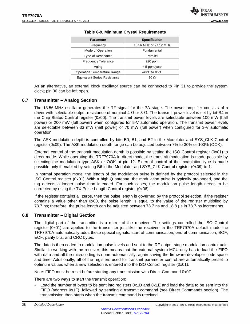
Any crystal used with TRF7970A should have minimum characteristics shown in Table 6-9.
Copyright © 2011–2014, Texas Instruments Incorporated Detailed Description 27Submit Documentation FeedbackProduct Folder Links: TRF7970A
TRF7970ASLOS743K –AUGUST 2011–REVISED APRIL 2014 www.ti.com
Table 6-9. Minimum Crystal Requirements
Parameter SpecificationFrequency 13.56 MHz or 27.12 MHz
Mode of Operation FundamentalType of Resonance Parallel
Frequency Tolerance ±20 ppmAging < 5 ppm/year
Operation Temperature Range -40°C to 85°CEquivalent Series Resistance 50 Ω
As an alternative, an external clock oscillator source can be connected to Pin 31 to provide the systemclock; pin 30 can be left open.
6.7 Transmitter – Analog SectionThe 13.56-MHz oscillator generates the RF signal for the PA stage. The power amplifier consists of adriver with selectable output resistance of nominal 4 Ω or 8 Ω. The transmit power level is set by bit B4 inthe Chip Status Control register (0x00). The transmit power levels are selectable between 100 mW (halfpower) or 200 mW (full power) when configured for 5-V automatic operation. The transmit power levelsare selectable between 33 mW (half power) or 70 mW (full power) when configured for 3-V automaticoperation.
The ASK modulation depth is controlled by bits B0, B1, and B2 in the Modulator and SYS_CLK Controlregister (0x09). The ASK modulation depth range can be adjusted between 7% to 30% or 100% (OOK).
External control of the transmit modulation depth is possible by setting the ISO Control register (0x01) todirect mode. While operating the TRF7970A in direct mode, the transmit modulation is made possible byselecting the modulation type ASK or OOK at pin 12. External control of the modulation type is madepossible only if enabled by setting B6 in the Modulator and SYS_CLK Control register (0x09) to 1.
In normal operation mode, the length of the modulation pulse is defined by the protocol selected in theISO Control register (0x01). With a high-Q antenna, the modulation pulse is typically prolonged, and thetag detects a longer pulse than intended. For such cases, the modulation pulse length needs to becorrected by using the TX Pulse Length Control register (0x06).
If the register contains all zeros, then the pulse length is governed by the protocol selection. If the registercontains a value other than 0x00, the pulse length is equal to the value of the register multiplied by73.7 ns; therefore, the pulse length can be adjusted between 73.7 ns and 18.8 µs in 73.7-ns increments.
6.8 Transmitter – Digital SectionThe digital part of the transmitter is a mirror of the receiver. The settings controlled the ISO Controlregister (0x01) are applied to the transmitter just like the receiver. In the TRF7970A default mode theTRF7970A automatically adds these special signals: start of communication, end of communication, SOF,EOF, parity bits, and CRC bytes.
The data is then coded to modulation pulse levels and sent to the RF output stage modulation control unit.Similar to working with the receiver, this means that the external system MCU only has to load the FIFOwith data and all the microcoding is done automatically, again saving the firmware developer code spaceand time. Additionally, all of the registers used for transmit parameter control are automatically preset tooptimum values when a new selection is entered into the ISO Control register (0x01).
Note: FIFO must be reset before starting any transmission with Direct Command 0x0F.
There are two ways to start the transmit operation:• Load the number of bytes to be sent into registers 0x1D and 0x1E and load the data to be sent into the
FIFO (address 0x1F), followed by sending a transmit command (see Direct Commands section). Thetransmission then starts when the transmit command is received.
28 Detailed Description Copyright © 2011–2014, Texas Instruments IncorporatedSubmit Documentation FeedbackProduct Folder Links: TRF7970A

TRF7970Awww.ti.com SLOS743K –AUGUST 2011–REVISED APRIL 2014
• Send the transmit command and the number of bytes to be transmitted first, and then start to send thedata to the FIFO. The transmission starts when first data byte is written into the FIFO.
NOTEIf the data length is longer than the FIFO, the TRF7970A notifies the external system MCUwhen most of the data from the FIFO has been transmitted by sending an interrupt requestwith a flag in the IRQ register to indicate a FIFO low or high status. The external systemshould respond by loading the next data packet into the FIFO.
At the end of a transmit operation, the external system MCU is notified by interrupt request (IRQ) with aflag in IRQ register (0x0C) indicating TX is complete (example value = 0x80).
The TX Length registers also support incomplete byte transmission. The high two nibbles in register 0x1Dand the nibble composed of bits B4 through B7 in register 0x1E store the number of complete bytes to betransmitted. Bit B0 in register 0x1E is a flag indicating that there are also additional bits to be transmittedthat do not form a complete byte. The number of bits is stored in bits B1 through B3 of the same register(0x1E).
Some protocols have options, and there are two sublevel configuration registers to select the TX protocoloptions.• ISO14443B TX Options register (0x02). This register controls the SOF and EOF selection and EGT
selection for the ISO14443B protocol.• ISO14443A High Bit Rate Options and Parity register (0x03). This register enables the use of different
bit rates for RX and TX operations in the ISO14443 high bit rate protocol and also selects the paritymethod in the ISO14443A high bit rate protocol.
The digital section also has a timer. The timer can be used to start the transmit operation at a specifiedtime in accordance with a selected event.
6.9 Transmitter – External Power Amplifier and Subcarrier DetectorThe TRF7970A can be used in conjunction with an external TX power amplifier or external subcarrierdetector for the receiver path. In this case, certain registers must be programmed as shown here:• Bit B6 of the Regulator and I/O Control register (0x0B) must be set to 1. This setting has two functions:
first, to provide a modulated signal for the transmitter if needed, and second, to configure theTRF7970A receiver inputs for an external demodulated subcarrier input.
• Bit B3 of the Modulation and SYS_CLK Control register (0x09) must be set to 1 (seeSection 6.14.3.2.8). This function configures the ASK/OOK pin for either a digital or analog output (B3= 0 enables a digital output, B3 = 1 enables an analog output). The design of an external poweramplifier requires detailed RF knowledge. There are also readily designed and certified high-power HFreader modules on the market.
Copyright © 2011–2014, Texas Instruments Incorporated Detailed Description 29Submit Documentation FeedbackProduct Folder Links: TRF7970A

TRF7970ASLOS743K –AUGUST 2011–REVISED APRIL 2014 www.ti.com
6.10 TRF7970A IC Communication Interface
6.10.1 General IntroductionThe communication interface to the reader can be configured in two ways: with a eight line parallelinterface (D0:D7) plus DATA_CLK, or with a three or four wire Serial Peripheral Interface (SPI). The SPIinterface uses traditional Master Out/Slave In (MOSI), Master In/Slave Out (MISO), IRQ, and DATA_CLKlines. The SPI can be operated with or without using the Slave Select line.
These communication modes are mutually exclusive; that is, only one mode can be used at a time in theapplication.
When the SPI interface is selected, the unused I/O_2, I/O_1, and I/O_0 pins must be hard-wired as shownin Table 6-10. At power up, the TRF7970A samples the status of these three pins and then enters one ofthe possible SPI modes.
The TRF7970A always behaves as the slave device, and the microcontroller (MCU) behaves as themaster device. The MCU initiates all communications with the TRF7970A, and the TRF7970A makes useof the Interrupt Request (IRQ) pin in both parallel and SPI modes to prompt the MCU for servicingattention.
Table 6-10. Pin Assignment in Parallel and Serial Interface Connection or Direct Mode
Pin Parallel Parallel (Direct Mode) SPI With SS SPI Without SS (1)
DATA_ CLK DATA_CLK DATA_CLK DATA_CLK from master DATA_CLK from masterI/O_7 A/D[7] (not used) MOSI (2) = data in (reader in) MOSI (2) = data in (reader in)
Direct mode, data out (subcarrierI/O_6 A/D[6] MISO (3) = data out (MCU out) MISO (3) = data out (MCU out)or bit stream)Direct mode, strobe – bit clockI/O_5 (4) A/D[5] See (4) See (4)out
I/O_4 A/D[4] (not used) SS – slave select (5) (not used)I/O_3 A/D[3] (not used) (not used) (not used)I/O_2 A/D[2] (not used) At VDD At VDDI/O_1 A/D[1] (not used) At VDD At VSS
I/O_0 A/D[0] (not used) At VSS At VSS
IRQ IRQ interrupt IRQ interrupt IRQ interrupt IRQ interrupt
(1) FIFO is not accessible in SPI without SS mode. See device errata for detailed information.(2) MOSI = Master Out, Slave In(3) MISO = Master In, Slave Out(4) I/O_5 pin is used only for information when data is put out of the chip (for example, reading 1 byte from the chip). It is necessary first to
write in the address of the register (8 clocks) and then to generate another 8 clocks for reading out the data. The I/O_5 pin goes highduring the second 8 clocks. But for normal SPI operations, I/O_5 pin is not used.
(5) Slave_Select pin is active low
30 Detailed Description Copyright © 2011–2014, Texas Instruments IncorporatedSubmit Documentation FeedbackProduct Folder Links: TRF7970A

TRF7970Awww.ti.com SLOS743K –AUGUST 2011–REVISED APRIL 2014
Communication is initialized by a start condition, which is expected to be followed by anAddress/Command word (Adr/Cmd). The Adr/Cmd word is 8 bits long, and Table 6-11 shows its format.
Table 6-11. Address and Command Word Bit Distribution
Bit Description Bit Function Address Command0 = addressB7 Command control bit 0 11 = command
0 = writeB6 Read/Write R/W 01 = readB5 Continuous address mode 1 = Continuous mode R/W 0B4 Address/Command bit 4 Adr 4 Cmd 4B3 Address/Command bit 3 Adr 3 Cmd 3B2 Address/Command bit 2 Adr 2 Cmd 2B1 Address/Command bit 1 Adr 1 Cmd 1B0 Address/Command bit 0 Adr 0 Cmd 0
The MSB (bit 7) determines if the word is to be used as a command or as an address. The last twocolumns of Table 6-11 show the function of the separate bits if either address or command is written. Datais expected once the address word is sent. In continuous-address mode (Cont. mode = 1), the first datathat follows the address is written (or read) to (from) the given address. For each additional data, theaddress is incremented by one. Continuous mode can be used to write to a block of control registers in asingle stream without changing the address; for example, setup of the predefined standard controlregisters from the MCU non-volatile memory to the reader. In non-continuous address mode (simpleaddressed mode), only one data word is expected after the address.
Address Mode is used to write or read the configuration registers or the FIFO. When writing more than 12bytes to the FIFO, the Continuous Address Mode should be set to 1.
The Command Mode is used to enter a command resulting in reader action (for example, initializetransmission, enable reader, and turn reader on or off).
Examples of expected communications between an MCU and the TRF7970A are shown in the followingsections.
Copyright © 2011–2014, Texas Instruments Incorporated Detailed Description 31Submit Documentation FeedbackProduct Folder Links: TRF7970A
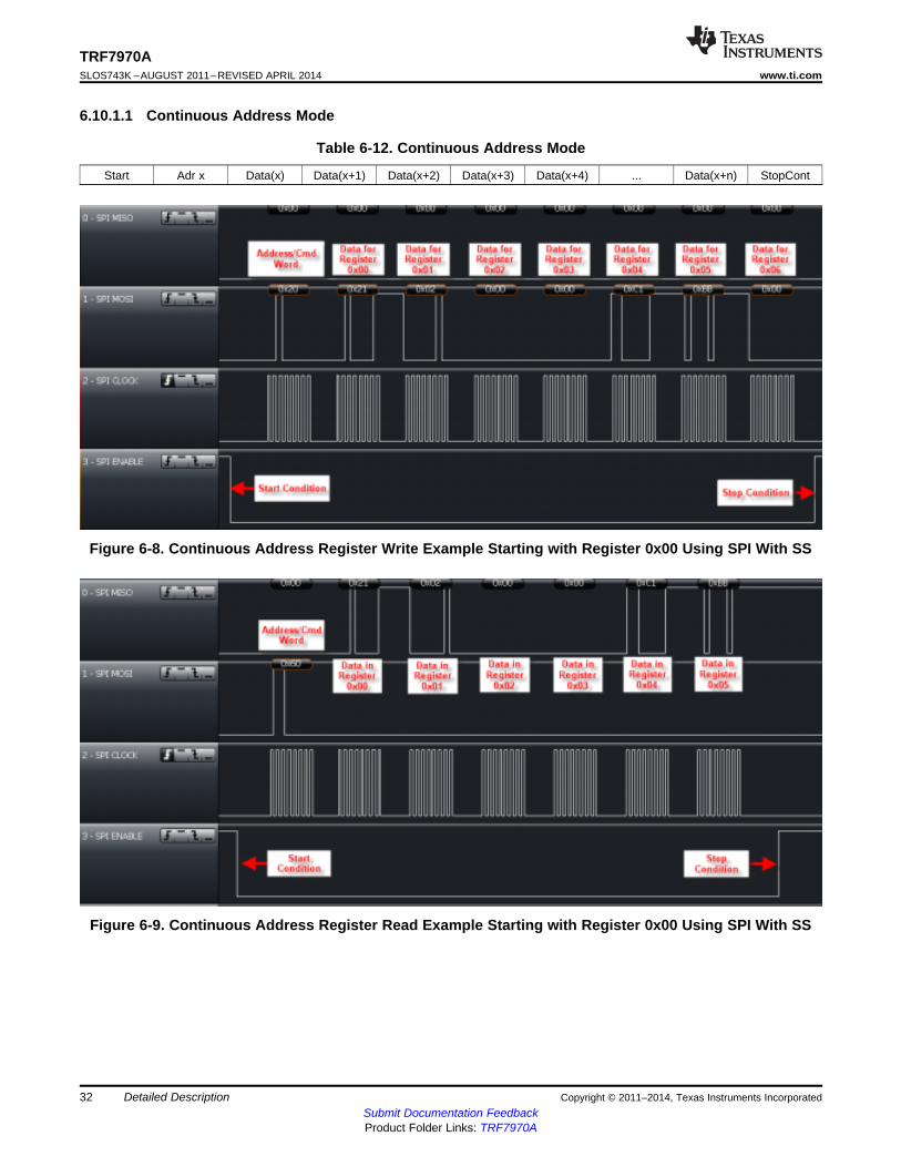
TRF7970ASLOS743K –AUGUST 2011–REVISED APRIL 2014 www.ti.com
6.10.1.1 Continuous Address Mode
Table 6-12. Continuous Address Mode
Start Adr x Data(x) Data(x+1) Data(x+2) Data(x+3) Data(x+4) ... Data(x+n) StopCont
Figure 6-8. Continuous Address Register Write Example Starting with Register 0x00 Using SPI With SS
Figure 6-9. Continuous Address Register Read Example Starting with Register 0x00 Using SPI With SS
32 Detailed Description Copyright © 2011–2014, Texas Instruments IncorporatedSubmit Documentation FeedbackProduct Folder Links: TRF7970A
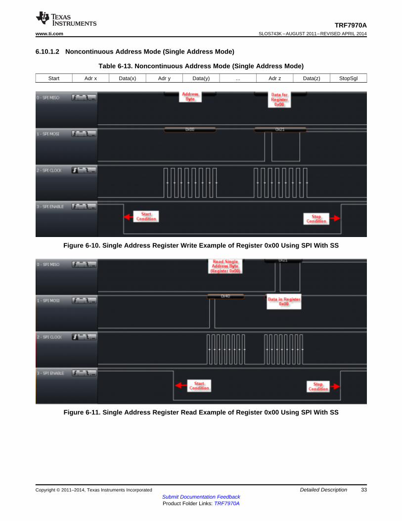
TRF7970Awww.ti.com SLOS743K –AUGUST 2011–REVISED APRIL 2014
6.10.1.2 Noncontinuous Address Mode (Single Address Mode)
Table 6-13. Noncontinuous Address Mode (Single Address Mode)
Start Adr x Data(x) Adr y Data(y) ... Adr z Data(z) StopSgl
Figure 6-10. Single Address Register Write Example of Register 0x00 Using SPI With SS
Figure 6-11. Single Address Register Read Example of Register 0x00 Using SPI With SS
Copyright © 2011–2014, Texas Instruments Incorporated Detailed Description 33Submit Documentation FeedbackProduct Folder Links: TRF7970A

TRF7970ASLOS743K –AUGUST 2011–REVISED APRIL 2014 www.ti.com
6.10.1.3 Direct Command Mode
Table 6-14. Direct Command Mode
Start Cmd x (Optional data or command) Stop
Figure 6-12. Direct Command Example of Sending 0x0F (Reset) Using SPI With SS
The other Direct Command Codes from MCU to TRF7970A IC are described in Section 6.13.
6.10.1.4 FIFO Operation
The FIFO is a 127-byte register at address 0x1F with byte storage locations 0 to 126. FIFO data is loadedin a cyclical manner and can be cleared by a reset command (0x0F) (see Figure 6-12 showing this DirectCommand).
Associated with the FIFO are two counters and three FIFO status flags. The first counter is a 7-bit FIFObyte counter (bits B0 to B6 in register 0x1C) that tracks the number of bytes loaded into the FIFO. If thenumber of bytes in the FIFO is n, the register value is n (number of bytes in FIFO register). For example, if8 bytes are in the FIFO, the FIFO counter (Register 0x1C) has the hexadecimal value of 0x08 (binaryvalue of 00001000).
A second counter (12 bits wide) indicates the number of bytes being transmitted (registers 0x1D and0x1E) in a data frame. An extension to the transmission-byte counter is a 4-bit broken-byte counter alsoprovided in register 0x1E (bits B0 to B3). Together these counters make up the TX length value thatdetermines when the reader generates the EOF byte.
FIFO status flags are as follows:• FIFO overflow (bit B7 of register 0x1C) – indicates that the FIFO has more than 127 bytes loaded
During transmission, the FIFO is checked for an almost-empty condition, and during reception for analmost-full condition. The maximum number of bytes that can be loaded into the FIFO in a singlesequence is 127 bytes.
NOTEThe number of bytes in a frame, transmitted or received, can be greater than 127 bytes.
34 Detailed Description Copyright © 2011–2014, Texas Instruments IncorporatedSubmit Documentation FeedbackProduct Folder Links: TRF7970A

TRF7970Awww.ti.com SLOS743K –AUGUST 2011–REVISED APRIL 2014
During transmission, the MCU loads the TRF7970A IC's FIFO (or during reception the MCU removes datafrom the FIFO), and the FIFO counter counts the number of bytes being loaded into the FIFO. Meanwhile,the byte counter keeps track of the number of bytes being transmitted. An interrupt request is generated ifthe number of bytes in the FIFO is less than 32 or greater than 96, so that MCU can send new data orremove the data as necessary. The MCU also checks the number of data bytes to be sent, so as to notsurpass the value defined in TX length bytes. The MCU also signals the transmit logic when the last byteof data is sent or was removed from the FIFO during reception. Transmission starts automatically after thefirst byte is written into FIFO.
Figure 6-13. Example of Checking the FIFO Status Register Using SPI With SS
6.10.2 Parallel Interface ModeIn parallel mode, the start condition is generated on the rising edge of the I/O_7 pin while the CLK is high.
This is used to reset the interface logic. Figure 6-14 shows the sequence of the data, with an 8-bit addressword first, followed by data.
Communication is ended by:• The StopSmpl condition, where a falling edge on the I/O_7 pin is expected while CLK is high.• The StopCont condition, where the I/O_7 pin must have a successive rising and falling edge while CLK
is low to reset the parallel interface and be ready for the new communication sequence.• The StopSmpl condition is also used to terminate the direct mode.
Figure 6-14. Parallel Interface Communication With Simple Stop Condition (StopSmpl)
Copyright © 2011–2014, Texas Instruments Incorporated Detailed Description 35Submit Documentation FeedbackProduct Folder Links: TRF7970A

TRF7970ASLOS743K –AUGUST 2011–REVISED APRIL 2014 www.ti.com
Figure 6-15. Parallel Interface Communication with Continuous Stop Condition (StopCont)
Figure 6-16. Example of Parallel Interface Communication With Continuous Stop Condition
6.10.3 Reception of Air Interface DataAt the start of a receive operation (when SOF is successfully detected), B6 is set in the IRQ Statusregister. An RX complete interrupt request is sent to the MCU at the end of the receive operation if thereceive data string is shorter than or equal to the number of bytes configured in the Adjustable FIFO IRQLevels register (0x14). An IRQ_FIFO interrupt request is sent to the MCU during the receive operation ifthe data string is greater than the level set in the Adjustable FIFO IRQ Levels register (0x14). Afterreceiving an IRQ_FIFO or RX complete interrupt, the MCU must read the FIFO status register (0x1C) todetermine the number of bytes to be read from the FIFO. Next, the MCU must read the data in the FIFO.It is optional to read the FIFO status register (0x1C) after reading FIFO data to determine if the receive iscomplete. In the case of an IRQ_FIFO, the MCU should expect either another IRQ_FIFO or RX completeinterrupt. This is repeated until an RX complete interrupt is generated. The MCU receives the interruptrequest, then checks to determine the reason for the interrupt by reading the IRQ Status register (0x0C),after which the MCU reads the data from the FIFO.
If the reader detects a receive error, the corresponding error flag is set (framing error, CRC error) in theIRQ Status register, indicating to the MCU that reception was not completed correctly.
36 Detailed Description Copyright © 2011–2014, Texas Instruments IncorporatedSubmit Documentation FeedbackProduct Folder Links: TRF7970A

TRF7970Awww.ti.com SLOS743K –AUGUST 2011–REVISED APRIL 2014
6.10.4 Data Transmission to MCUBefore beginning data transmission, the FIFO should always be cleared with a reset command (0x0F).Data transmission is initiated with a selected command (see Section 6.13). The MCU then commands thereader to do a continuous write command (0x3D) starting from register 0x1D. Data written into register0x1D is the TX Length Byte 1 (upper and middle nibbles), while the following byte in register 0x1E is theTX Length Byte 2 (lower nibble and broken byte length) (see Table 6-57 and Table 6-58) . Note that theTX byte length determines when the reader sends the end of frame (EOF) byte. After the TX length bytesare written, FIFO data is loaded in register 0x1F with byte storage locations 0 to 127. Data transmissionbegins automatically after the first byte is written into the FIFO. The loading of TX length bytes and theFIFO can be done with a continuous-write command, as the addresses are sequential.
At the start of transmission, the flag B7 (IRQ_TX) is set in the IRQ Status register, and at the end of thetransmit operation, an interrupt is sent to inform the MCU that the task is complete.
6.10.5 Serial Interface Communication (SPI)When an SPI interface is used, I/O pins I/O_2, I/O_1, and I/O_0 must be hard wired according to Table 6-10. On power up, the TRF7970A looks for the status of these pins and then enters into the correspondingmode.
The choice of one of these modes over another should be predicated by the available GPIOs and thedesired control of the system.
The serial communications work in the same manner as the parallel communications with respect to theFIFO, except for the following condition. On receiving an IRQ from the reader, the MCU reads theTRF7970A IRQ Status register to determine how to service the reader. After this, the MCU must to do adummy read to clear the reader's IRQ status register. The dummy read is required in SPI mode becausethe reader's IRQ status register needs an additional clock cycle to clear the register. This is not required inparallel mode because the additional clock cycle is included in the Stop condition. When first establishingcommunications with the TRF7970A, the SOFT_INIT (0x03) and IDLE (0x00) commands should be sentfirst from the MCU (see Table 6-19).
Copyright © 2011–2014, Texas Instruments Incorporated Detailed Description 37Submit Documentation FeedbackProduct Folder Links: TRF7970A

Read Data inIRQ Status Register
Dummy ReadWrite AddressByte (0x6C)
No Data Transitions (All High or Low)
Don’t Care Ignore
B7 B6 B5 B4 B3 B2 B1 B0
SLAVE
SELECT
MISO
MOSI
DATA _CLK
No Data Transitions (All High or Low)
B7 B6 B5 B4 B3 B2 B1 B0
TRF7970ASLOS743K –AUGUST 2011–REVISED APRIL 2014 www.ti.com
The procedure for a dummy read is as follows:1. Start the dummy read:
(a) When using slave select (SS): set SS bit low.(b) When not using SS: start condition is when Data Clock is high (see Table 6-10).
2. Send address word to IRQ status register (0x0C) with read and continuous address mode bits set to 1(see Table 6-10).
3. Read 1 byte (8 bits) from IRQ status register (0x0C).4. Dummy-read 1 byte from register 0x0D (collision position and interrupt mask).5. Stop the dummy read:
(a) When using slave select (SS): set SS bit high.(b) When not using SS: stop condition when Data Clock is high.
Figure 6-17. Procedure for Dummy Read
Figure 6-18. Example of Dummy Read Using SPI With SS
38 Detailed Description Copyright © 2011–2014, Texas Instruments IncorporatedSubmit Documentation FeedbackProduct Folder Links: TRF7970A

SLAVE
SELECT
MISO
MOSI
DATA
CLK
WRITE
ADDRESS BYTE
READ DATA
BYTE 1
READ DATA
BYTE n
DON’T CARE
No Data Transitions (All High or Low) No Data Transitions (All High or Low)B7 B6 B5 B4 B3 B2 B1 B0
B7 B6 B5 B4 B3 B2 B1 B0 B7 B6 B5 B4 B3 B2 B1 B0
b0MISO
MOSI
DATA
CLK
WRITEMOSI Transitions on Data Clock
Rising Edge
MOSI Valid on Data Clock Falling Edge
tSTE,LEAD
b7
tLO/HI tLO/HI
b6…b1 b0
tSU,SI tHD,SI
1/fUCxCLKtSTE,DIS
b6...b1
tVALID,SO
tSTE,LAG
tHD,SO
DON’T CARE
READData Transition is on Data Clock
Rising Edge
MISO Valid on Data Clock Falling Edge
tSU,SO
b7
NO DATA TRANSITIONS
(ALL HIGH/LOW)
Slave
Select
TRF7970Awww.ti.com SLOS743K –AUGUST 2011–REVISED APRIL 2014
6.10.5.1 Serial Interface Mode With Slave Select (SS)
The serial interface is in reset while the Slave Select signal is high. Serial data in (MOSI) changes on therising edge, and is validated in the reader on the falling edge, as shown in Figure 6-19. Communication isterminated when the Slave Select signal goes high.
All words must be 8 bits long with the MSB transmitted first.
Figure 6-19. SPI With Slave Select Timing Diagram
The read command is sent out on the MOSI pin, MSB first, in the first eight clock cycles. MOSI datachanges on the rising edge, and is validated in the reader on the falling edge, as shown in Figure 6-19.During the write cycle, the serial data out (MISO) is not valid. After the last read command bit (B0) isvalidated at the eighth falling edge of SCLK, valid data can be read on the MISO pin at the falling edge ofSCLK. It takes eight clock edges to read out the full byte (MSB first). See Section 5.3 for electricalspecifications related to Figure 6-19.
The continuous read operation is shown in Figure 6-20.
Figure 6-20. Continuous Read Operation Using SPI With Slave Select
Copyright © 2011–2014, Texas Instruments Incorporated Detailed Description 39Submit Documentation FeedbackProduct Folder Links: TRF7970A

TRF7970ASLOS743K –AUGUST 2011–REVISED APRIL 2014 www.ti.com
Figure 6-21. Continuous Read of Registers 0x00 Through 0x05 Using SPI With SS
Performing Single Slot Inventory Command as an example is shown in Figure 6-22. Reader registers (inthis example) are configured for 5 VDC in and default operation.
Figure 6-22. Inventory Command Sent From MCU to TRF7970A
The TRF7970A takes these bytes from the MCU and then send out Request Flags, Inventory Command,and Mask over the air to the ISO15693 transponder. After these three bytes have been transmitted, aninterrupt occurs to indicate back to the reader that the transmission has been completed. In the example inFigure 6-23, this IRQ occurs approximately 1.6 ms after the SS line goes high after the Inventorycommand is sent out.
40 Detailed Description Copyright © 2011–2014, Texas Instruments IncorporatedSubmit Documentation FeedbackProduct Folder Links: TRF7970A

TRF7970Awww.ti.com SLOS743K –AUGUST 2011–REVISED APRIL 2014
Figure 6-23. IRQ After Inventory Command
The IRQ status register read (0x6C) yields 0x80, which indicates that TX is indeed complete. This isfollowed by a dummy clock. Then, if a tag is in the field and no error is detected by the reader, a secondinterrupt is expected and occurs (in this example) approximately 4 ms after first IRQ is read and cleared.
In the continuation of the example (see Figure 6-24), the IRQ Status Register is read using methodpreviously recommended, followed by a single read of the FIFO status register, which indicates that thereare 10 bytes to be read out.
Figure 6-24. Read IRQ Status Register After Inventory Command
This is then followed by a continuous read of the FIFO. The first byte is (and should be) 0x00 for no error.The next byte is the DSFID (usually shipped by manufacturer as 0x00), then the UID, shown here up tothe next most significant byte, the MFG code (shown as 0x07 (TI silicon)).
Copyright © 2011–2014, Texas Instruments Incorporated Detailed Description 41Submit Documentation FeedbackProduct Folder Links: TRF7970A

TRF7970ASLOS743K –AUGUST 2011–REVISED APRIL 2014 www.ti.com
Figure 6-25. Continuous Read of FIFO After Inventory Command
At this point, it is good form to reset the FIFO and then read out the RSSI value of the tag. In this case thetransponder is very close to the antenna, so value of 0x7F is recovered.
Figure 6-26. Reset FIFO and Read RSSI
42 Detailed Description Copyright © 2011–2014, Texas Instruments IncorporatedSubmit Documentation FeedbackProduct Folder Links: TRF7970A

Analog Front End (AFE)
14443A
ISO Encoders/Decoders
14443B 15693 FeliCa
Packetization/Framing
Microcontroller
Direct Mode 0:Raw RF Sub-Carrier
Data Stream
Direct Mode 1:Raw Digital ISO Coded
Data WithoutProtocol Frame
ISO Mode:Full ISO Framing
and Error Checking(Typical Mode)
TRF7970Awww.ti.com SLOS743K –AUGUST 2011–REVISED APRIL 2014
6.10.6 Direct ModeDirect mode allows the user to configure the reader in one of two ways. Direct Mode 0 (bit 6 = 0, asdefined in ISO Control register) allows the user to use only the front-end functions of the reader,bypassing the protocol implementation in the reader. For transmit functions, the user has direct access tothe transmit modulator through the MOD pin (pin 14). On the receive side, the user has direct access tothe subcarrier signal (digitized RF envelope signal) on I/O_6 (pin 23).
Direct Mode 1 (bit 6 = 1, as defined in ISO Control register) uses the subcarrier signal decoder of theselected protocol (as defined in ISO Control register). This means that the receive output is not thesubcarrier signal but the decoded serial bit stream and bit clock signals. The serial data is available onI/O_6 (pin 23) and the bit clock is available on I/O_5 (pin 22). The transmit side is identical; the user hasdirect control over the RF modulation through the MOD input. This mode is provided so that the user canimplement a protocol that has the same bit coding as one of the protocols implemented in the reader, butneeds a different framing format.
To select direct mode, the user must first choose which direct mode to enter by writing B6 in the ISOControl register. This bit determines if the receive output is the direct subcarrier signal (B6 = 0) or theserial data of the selected decoder. If B6 = 1, then the user must also define which protocol should beused for bit decoding by writing the appropriate setting in the ISO Control register.
The reader actually enters the direct mode when B6 (direct) is set to 1 in the chip status control register.Direct mode starts immediately. The write command should not be terminated with a stop condition (seecommunication protocol), because the stop condition terminates the direct mode and clears B6. This isnecessary as the direct mode uses one or two I/O pins (I/O_6, I/O_5). Normal parallel communication isnot possible in direct mode. Sending a stop condition terminates direct mode.
Figure 6-27 shows the different configurations available in direct mode.• In mode 0, the reader is used as an AFE only, and protocol handling is bypassed.• In mode 1, framing is not done, but SOF and EOF are present. This allows for a user-selectable
framing level based on an existing ISO standard.• In mode 2, data is ISO-standard formatted. SOF, EOF, and error checking are removed, so the
microprocessor receives only bytes of raw data through a 127-byte FIFO.
Figure 6-27. User-Configurable Modes
The steps to enter Direct Mode are listed below, using SPI with SS communication method only as oneexample, as Direct Modes are also possible with parallel and SPI without SS. The must enter Direct Mode0 to accommodate non-ISO standard compliant card type communications. Direct Mode can be entered atany time, so in the event a card type started with ISO standard communications, then deviated from thestandard after being identified and selected, the ability to go into Direct Mode 0 becomes very useful.
Copyright © 2011–2014, Texas Instruments Incorporated Detailed Description 43Submit Documentation FeedbackProduct Folder Links: TRF7970A
TRF7970ASLOS743K –AUGUST 2011–REVISED APRIL 2014 www.ti.com
Step 1: Configure Pins I/O_0 to I/O_2 for SPI with SS
Step 2: Set Pin 12 of the TRF7970A (ASK/OOK pin) to 0 for ASK or 1 for OOK
Step 3: Program the TRF7970A registers
The following registers need to be explicitly set before going into the Direct Mode.1. ISO Control register (0x01) to the appropriate standard
– 0x02 for ISO 15693 High Data Rate– 0x08 for ISO14443A (106 kbps)– 0x1A for FeliCa 212 kbps– 0x1B for FeliCa 424 kbps
2. Modulator and SYS_CLK register (0x09) to the appropriate clock speed and modulation– 0x21 for 6.78 MHz Clock and OOK (100%) modulation– 0x20 for 6.78 MHz Clock and ASK 10% modulation– 0x22 for 6.78 MHz Clock and ASK 7% modulation– 0x23 for 6.78 MHz Clock and ASK 8.5% modulation– 0x24 for 6.78 MHz Clock and ASK 13% modulation– 0x25 for 6.78 MHz Clock and ASK 16% modulation
(See register 0x09 definition for all other possible values)
Example register setting for ISO14443A at 106 kbps:• ISO Control register (0x01) to 0x08• RX No Response Wait Time register (0x07) to 0x0E• RX Wait Time register (0x08) to 0x07• Modulator control register (0x09) to 0x21 (or any custom modulation)• RX Special Settings register (0x0A) to 0x20
44 Detailed Description Copyright © 2011–2014, Texas Instruments IncorporatedSubmit Documentation FeedbackProduct Folder Links: TRF7970A

TRF7970Awww.ti.com SLOS743K –AUGUST 2011–REVISED APRIL 2014
Step 4: Entering Direct Mode 0
The following registers need to be programmed to enter Direct Mode 01. Set bit B6 of the Modulator and SYS_CLK Control register (0x09) to 1.2. Set bit B6 of the ISO Control (Register 01) to 0 for Direct Mode 0 (default its 0)3. Set bit B6 of the Chip Status Control register (0x00) to 1 to enter Direct Mode4. Send extra eight clock cycles (see Figure 6-28, this step is TRF7970A specific)
NOTE– It is important that the last write is not terminated with a stop condition. For SPI, this
means that Slave Select (I/O_4) stays low.– Sending a Stop condition terminates the Direct Mode and clears bit B6 in the Chip Status
Control register (0x00).
NOTEAccess to Registers, FIFO, and IRQ is not available during Direct Mode 0.
The reader enters the Direct Mode 0 when bit 6 of the Chip Status Control register (0x00) is set to a 1 andstays in Direct Mode 0 until a stop condition is sent from the microcontroller.
NOTEThe write command should not be terminated with a stop condition (for example, in SPImode this is done by bringing the Slave Select line high after the register write), because thestop condition terminates the direct mode and clears bit 6 of the Chip Status Control register(0x00), making it a 0.
Figure 6-28. Entering Direct Mode 0
Copyright © 2011–2014, Texas Instruments Incorporated Detailed Description 45Submit Documentation FeedbackProduct Folder Links: TRF7970A

TRF7970A Microcontroller
Drive the MOD pinaccording to the data codingspecified by the standard
Decode the subcarrierinformation accordingto the standard
MOD(Pin 14)
I/O_6(Pin 23)
TRF7970ASLOS743K –AUGUST 2011–REVISED APRIL 2014 www.ti.com
Step 5: Transmit Data Using Direct Mode
The application now has direct control over the RF modulation through the MOD input (see Figure 6-29).
Figure 6-29. Direct Control Signals
The microcontroller is responsible for generating data according to the coding specified by the particularstandard. The microcontroller must generate SOF, EOF, Data, and CRC. In direct mode, the FIFO is notused and no IRQs are generated. See the applicable ISO standard to understand bit and framedefinitions. As an example of what the developer sees when using DM0 in an actual application, Figure 6-30 is presented to clearly show the relationship between the MOD pin being controlled by the MCU andthe resulting modulated 13.56-MHz carrier signal.
Figure 6-30. TX Sequence Out in DM0
Step 6: Receive Data Using Direct Mode
After the TX operation is complete, the tag responds to the request and the subcarrier data is available onpin I/O_6. The microcontroller needs to decode the subcarrier signal according to the standard. Thisincludes decoding the SOF, data bits, CRC, and EOF. The CRC then needs to be checked to verify dataintegrity. The receive data bytes must be buffered locally.
As an example of the receive data bits and framing level according to the ISO14443A standard is shownin Figure 6-31 (taken from ISO14443 specification and TRF7970A air interface).
46 Detailed Description Copyright © 2011–2014, Texas Instruments IncorporatedSubmit Documentation FeedbackProduct Folder Links: TRF7970A

?
?
?
128/fc = 9.435 µs = t (106-kbps data rate)
64/fc = 4.719 µs = t time
32/fc = 2.359 µs = t time
b
x
1
t = 9.44b µs t = 4.72x µs t = 2.481 µs
Sequence Y = Carrier for 9.44 µs Sequence Z = Pause for 2Carrier for Remainder of 9.44
to 3 µs,µs
TRF7970Awww.ti.com SLOS743K –AUGUST 2011–REVISED APRIL 2014
Figure 6-31. Receive Data Bits and Framing Level
Figure 6-32 is presented to clearly show an example of what the developer should expect on the I/O_6line during the RX process while in Direct Mode 0.
Copyright © 2011–2014, Texas Instruments Incorporated Detailed Description 47Submit Documentation FeedbackProduct Folder Links: TRF7970A

TRF7970ASLOS743K –AUGUST 2011–REVISED APRIL 2014 www.ti.com
Figure 6-32. RX Sequence on I/O_6 in DM0 (Analog Capture)
Step 7: Terminating Direct Mode 0
After the EOF is received, data transmission is over, and Direct Mode 0 can be terminated by sending aStop Condition (in the case of SPI, make the Slave Select go high). The TRF7970A is returned to defaultstate.
6.11 Special Direct Mode for Improved MIFARE™ CompatibilitySee the application report TRF7970A Firmware Design Hints (SLOA159).
6.12 NFC Modes
6.12.1 TargetWhen used as the NFC target, the chip is typically in a power down or standby mode. If EN2 = H, the chipkeeps the supply system on. If EN2 = L and EN = L the chip is in complete power down. To operate asNFC target or Tag emulator, the MCU must load a value different from zero (0) in Target Detection Levelregister (b0-b2) which enables the RF measurement system (supplied by VEXT, so it can operate alsoduring complete power down and consumes only 3.5 µA). The RF measurement constantly monitors theRF signal on the antenna input. When the RF level on the antenna input exceeds the level defined in thein Target Detection Level register, the chip is automatically activated (EN is internal forced high). Thetypical RF value that causes power-up for each value of B0 to B2 and the function of Target DetectionLevel register is listed in Table 6-15.NFC Target Detection Level Register (0x18) – defines level for RF level for wake-up and givesinformation of NFCID size. This register is directly supplied by VEXT to ensure data retention duringcomplete power down.
48 Detailed Description Copyright © 2011–2014, Texas Instruments IncorporatedSubmit Documentation FeedbackProduct Folder Links: TRF7970A

TRF7970Awww.ti.com SLOS743K –AUGUST 2011–REVISED APRIL 2014
Table 6-15. NFC Target Detection Level Register
Bit Signal Name Function CommentsB7 Id_s1
NFCID1 size used in 106 kbps passive target SDDB6 Id_s0
Automatic SDD using internal state machine and IDB5 Sdd_en 1 = Enables internal SDD protocol stored in NFCID Number register (1)
B4 N/AB3 Hi_rf Extended range for RF measurementsB2 Rfdet_h2
RF field level required for system wake-up. If all Comparator output is displayed in NFC TargetB1 Rfdet_h1 bits are 0, the RF level detection is switched off. Protocol register B7 (rf_h)B0 Rfdet_h0
(1) Refer to the device errata (SLOZ011) for details on automatic SDD dependencies.
Default: reset to 00 at POR on VEXT (not on POR based on VDD_X), not reset at EN = 0
Table 6-16. Bits B0 to B3 of the NFC Target Detection Level Register
b0 B1 B2 000 001 010 011 100 101 110 111B3 = 0 RF Vpp Not active 480 mV 350 mV 250 mV 220 mV 190 mV 180 mV 170 mVB3 = 1 RF Vpp Not active 1500 mV 700 mV 500 mV 450 mV 400 mV 320 mV 280 mV
When the voltage supply system and the oscillator are started and is stable, the osc_ok goes high (B6 ofRSSI Level and Oscillator Status register) and IRQ is sent with bit B2 = 1 of IRQ register (field change).Bit B7 NFC Target Protocol in register directly displays the status of RF level detection (running constantlyalso during normal operation). This informs the MCU that the chip should start operation as an NFCTARGET device.
When the first command from the INITIATOR is received another IRQ sent with B6 (RX start) set in IRQregister. The MCU must set EN = H (confirm the power-up) in the time between the two IRQs as theinternal power-up ends after the second IRQ. The type and coding of the first initiator (or reader in thecase of a tag emulator) command define the communication protocol type which the target must use. Sothe communication protocol type is available in the NFC Target Protocol register immediately afterreceiving the first command. The coding of the NFC Target Protocol register is described next.
NFC Target Protocol Register (0x19) – displays the bit rate and protocol type (active or passive)transmitted by initiator in the first command. It also displays the comparator outputs of both RF leveldetectors.
Table 6-17. NFC Target Protocol Register
Bit Signal Name Function CommentsThe wake-up level is defined by bits b0-b3 of NFCB7 Rf_h 1 = RF level is above the set wake-up level Target Detection Level register
1 = RF level is above the RF collision avoidance The collision avoidance level is defined by bits b0-B6 Rf_l level. b2 of NFC Low Field Detection Level registerB5 N/A
1 = FeliCa type The first initiator command had physical levelB4 FeliCa 0 = ISO14443A type coding like FeliCa or like ISO14443AThe first initiator/reader command was SENS_REQB3 Pas106 Passive target 106 kbps or tag emulation or ALL_REQ
B2 Pas14443B Tag emulation ISO14443B The first reader command was of ISO14443B typeB1 Nfcbr1 00 = N/A
01 = 106 kbpsBit rate of first received command 10 = 212 kbpsB0 Nfcbr011 = 424 kbps
Copyright © 2011–2014, Texas Instruments Incorporated Detailed Description 49Submit Documentation FeedbackProduct Folder Links: TRF7970A

TRF7970ASLOS743K –AUGUST 2011–REVISED APRIL 2014 www.ti.com
Default: reset to 00 at POR and EN = L. B0 to B4 are automatically reset after MCU read operation. B6and B7 continuously display the RF level comparator outputs.
Based on the first command from INITIATOR following actions are taken:• If the first command is SENS_REQ or ALL_REQ, the TARGET must enter the SDD protocol for 106
kbps passive communication. If bit B5 in NFC Target Detection Level register is not set, the MCUhandles the SDD and the command received is send to FIFO. If the RF field is turned off (B7 in theNFC Target Protocol register goes low) at any time, the system sends an IRQ to the MCU with bit B2(RF field change) in the IRQ register set high. This informs the MCU that the procedure was abortedand the system must be reset. The clock extractor is automatically activated in this mode.
• If the command is SENS_REQ or ALL_REQ and the Tag emulation bit in ISO Control register is set,the system emulates an ISO14443A tag. The procedure does not differ from the one previouslydescribed for a passive target at 106 kbps. The clock extractor is automatically activated in this mode.
• If the first command is a POLLING request, the system becomes a TARGET in passive communicationusing 212 kbps or 424 kbps. The SDD is relatively simple and is handled by the MCU directly. ThePOLLING response is sent in one of the slots automatically calculated by the MCU (first slot starts2.416 ms after the end of the command and slots follow in 1.208 ms).
• If the first command is ATR_REQ, the system operates as an active TARGET using the samecommunication speed and bit coding as used by the INITIATOR. Again, all of the replies are handledby MCU. The chip is only required to time the response collision avoidance, which is done on directcommand from MCU. When the RF field is switched on and the minimum wait time is elapsed, the chipsends an IRQ with B1 (RF collision avoidance finished) set high. This signals the MCU that it can sendthe reply.
• If the first command is coded as ISO14443B and the Tag emulation bit is set in the ISO Controlregister, the system enters ISO14443B emulator mode. The anticollision must be handled by the MCU,and the chip provides all physical level coding, decoding, and framing for this protocol.
Table 6-18 shows the function of the IRQ and Status register in NFC and Tag emulation. This register ispreset to 0 at POR = H or EN = L and at each write to ISO Control. It is also automatically reset at the endof read phase. The reset also removes the IRQ flag.
Table 6-18. IRQ and Status Register (0x0C) for NFC and Card Emulation Operation (1)
Bit Name Function DescriptionSignals that TX is in progress. The flag is set at the start of
B7 Irq_tx IRQ set due to end of TX TX but the interrupt request (IRQ = 1) is sent when TX isfinished.Signals that RX SOF was received and RX is in progress.
B6 Irg_srx IRQ set due to RX start The flag is set at the start of RX but the interrupt request(IRQ = 1) is sent when RX is finished.Signals FIFO high or low as set in the Adjustable FIFO IRQB5 Irq_fifo Signals the FIFO level Levels (0x14) registerIndicates receive CRC error only if B7 (no RX CRC) of ISOB4 Irq_err1 CRC error Control register is set to 0.
B3 Irq_err2 Parity error Indicates parity error for ISO14443AB2 Irq_err3 Byte framing or EOF error Indicates framing error
Collision error for ISO14443A and ISO15693 singlesubcarrier. Bit is set if more then 6 or 7 (as defined in
B1 Irq_col Collision error register 0x01) are detected inside one bit period ofISO14443A 106 kbps. Collision error bit can also betriggered by external noise.No response within the "No-response time" defined in RX
B0 Irq_noresp No-response time interrupt No-response Wait Time register (0x07). Signals the MCUthat next slot command can be sent. Only for ISO15693.
(1) Displays the cause of IRQ and TX/RX status
50 Detailed Description Copyright © 2011–2014, Texas Instruments IncorporatedSubmit Documentation FeedbackProduct Folder Links: TRF7970A

TRF7970Awww.ti.com SLOS743K –AUGUST 2011–REVISED APRIL 2014
6.12.2 InitiatorThe chip is fully controlled by the MCU as in RFID reader operation. The MCU activates the chip andwrites the mode selection in the ISO Control register. The MCU uses RF collision avoidance commands,so it is relieved of any real-time task. The normal transmit and receive procedure (through the FIFO) areused to communicate with the TARGET device as described in Section 6.10.
6.13 Direct Commands from MCU to Reader
6.13.1 Command Codes
Table 6-19. Address and Command Word Bit Distribution
Command Code Command Comments0x00 Idle0x03 Software Initialization Same as Power on Reset0x04 Perform RF Collision Avoidance0x05 Perform response RF Collision Avoidance0x06 Perform response RF Collision Avoidance (n = 0)0x0F Reset0x10 Transmission without CRC0x11 Transmission with CRC0x12 Delayed Transmission without CRC0x13 Delayed Transmission with CRC0x14 End of Frame/Transmit Next Time Slot ISO156930x15 Close Slot Sequence0x16 Block Receiver0x17 Enable Receiver0x18 Test internal RF (RSSI at RX input with TX off)0x19 Test external RF (RSSI at RX input with TX on)0x1A Receiver Gain Adjust
The command code values from Table 6-19 are substituted in Table 6-20, Bits 0 through 4. Also, themost-significant bit (MSB) in Table 6-20 must be set to 1. ( Table 6-20 is same as Table 6-11, shown hereagain for user clarity).
Table 6-20. Address and Command Word Bit Distribution
Bit Description Bit Function Address Command0 = addressB7 Command control bit 0 11 = command
0 = writeB6 Read/Write R/W 01 = readB5 Continuous address mode 1 = Continuous mode R/W 0B4 Address/Command bit 4 Adr 4 Cmd 4B3 Address/Command bit 3 Adr 3 Cmd 3B2 Address/Command bit 2 Adr 2 Cmd 2B1 Address/Command bit 1 Adr 1 Cmd 1B0 Address/Command bit 0 Adr 0 Cmd 0
Copyright © 2011–2014, Texas Instruments Incorporated Detailed Description 51Submit Documentation FeedbackProduct Folder Links: TRF7970A

TRF7970ASLOS743K –AUGUST 2011–REVISED APRIL 2014 www.ti.com
The MSB determines if the word is to be used as a command or address. The last two columns ofTable 6-20 show the function of each bit, depending on whether address or command is written.Command mode is used to enter a command resulting in reader action (initialize transmission, enablereader, and turn reader on or off).
6.13.1.1 Idle (0x00)
This command issues dummy clock cycles. In parallel mode, one cycle is issued. In SPI mode, eightcycles are issued.
6.13.1.2 Software Initialization (0x03)
This command starts a Power on Reset. After sending this command, the register values change asshown in Table 6-21.
Table 6-21. Register Values After Sending SoftwareInitialization (0x03)
Address Register Value0x00 Chip Status Control 0x010x01 ISO Control 0x21 (1)
0x02 ISO14443B TX options 0x000x03 ISO14443A high bit rate options 0x000x04 TX timer setting, H-byte 0xC1 (1)
0x05 TX timer setting, L-byte 0xC1 (1)
0x06 TX pulse-length control 0x000x07 RX no response wait 0x0E0x08 RX wait time 0x07 (1)
0x09 Modulator and SYS_CLK control 0x910x0A RX Special Setting 0x10 (1)
0x0B Regulator and I/O control 0x870x0C IRQ status 0x000x0D Collision position and interrupt mask 0x3E0x0E Collision position 0x000x0F RSSI levels and oscillator status 0x400x10 Special Function 0x000x11 Special Function 0x000x12 RAM 0x000x13 RAM 0x000x14 Adjustable FIFO IRQ Levels 0x000x15 Reserved 0x000x16 NFC Low Field Detection Level 0x000x18 NFC Target Detection Level 0x000x19 NFC Target Protocol 0x000x1A Test 0x000x1B Test 0x000x1C FIFO status 0x00
(1) Differs from default at POR
52 Detailed Description Copyright © 2011–2014, Texas Instruments IncorporatedSubmit Documentation FeedbackProduct Folder Links: TRF7970A

TRF7970Awww.ti.com SLOS743K –AUGUST 2011–REVISED APRIL 2014
6.13.1.3 Initial RF Collision Avoidance (0x04)
This command executes the initial collision avoidance and sends out IRQ after 5 ms from establishing RFfield (so the MCU can start sending commands/data). If the external RF field is present (higher than thelevel set in NFC Low Field Detection Level register (0x16)) then the RF field can not be switched on andhence a different IRQ is returned.
6.13.1.4 Response RF Collision Avoidance (0x05)
This command executes the response collision avoidance and sends out IRQ after 75 µs from establishing
RF field (so the MCU can start sending commands/data). If the external RF field is present (higher thanthe level set in NFC Low Field Detection Level register (0x16)) then the RF field can not be switched onand hence a different IRQ is returned.
6.13.1.5 Response RF Collision Avoidance (0x06, n = 0)
This command executes the response collision avoidance without random delay. It sends out IRQ after 75µs from establishing RF field (so the MCU can start sending commands/data). If the external RF field ispresent (higher than the level set in NFC Low Field Detection Level register (0x16)) then the RF field cannot be switched on and hence a different IRQ is returned.
6.13.1.6 Reset (0x0F)
The reset command clears the FIFO contents and FIFO status register (0x1C). It also clears the registerstoring the collision error location (0x0E).
6.13.1.7 Transmission With CRC (0x11)
The transmission command must be sent first, followed by transmission length bytes, and FIFO data. Thereader starts transmitting after the first byte is loaded into the FIFO. The CRC byte is included in thetransmitted sequence.
6.13.1.8 Transmission Without CRC (0x10)
Same as Section 6.13.1.7 with CRC excluded.
6.13.1.9 Delayed Transmission With CRC (0x13)
The transmission command must be sent first, followed by the transmission length bytes, and FIFO data.
The reader transmission is triggered by the TX timer.
6.13.1.10 Delayed Transmission Without CRC (0x12)
Same as Section 6.13.1.9 with CRC excluded.
6.13.1.11 Transmit Next Time Slot (0x14)
When this command is received, the reader transmits the next slot command. The next slot sign is definedby the protocol selection.
6.13.1.12 Block Receiver (0x16)
The block receiver command puts the digital part of receiver (bit decoder and framer) in reset mode. Thisis useful in an extremely noisy environment, where the noise level could otherwise cause a constantswitching of the subcarrier input of the digital part of the receiver. The receiver (if not in reset) would try tocatch a SOF signal, and if the noise pattern matched the SOF pattern, an interrupt would be generated,falsely signaling the start of an RX operation. A constant flow of interrupt requests can be a problem for
Copyright © 2011–2014, Texas Instruments Incorporated Detailed Description 53Submit Documentation FeedbackProduct Folder Links: TRF7970A

TRF7970ASLOS743K –AUGUST 2011–REVISED APRIL 2014 www.ti.com
the external system (MCU), so the external system can stop this by putting the receive decoders in resetmode. The reset mode can be terminated in two ways. The external system can send the enable receivercommand. The reset mode is also automatically terminated at the end of a TX operation. The receiver canstay in reset after end of TX if the RX wait time register (0x08) is set. In this case, the receiver is enabledat the end of the wait time following the transmit operation.
6.13.1.13 Enable Receiver (0x17)
This command clears the reset mode in the digital part of the receiver if the reset mode was entered bythe block receiver command.
6.13.1.14 Test Internal RF (RSSI at RX Input With TX ON) (0x18)
The level of the RF carrier at RF_IN1 and RF_IN2 inputs is measured. Operating range between 300 mVPand 2.1 VP (step size is 300 mV). The two values are displayed in the RSSI levels register (0x0F). Thecommand is intended for diagnostic purposes to set correct RF_IN levels. Optimum RFIN input level isapproximately 1.6 VP or code 5 to 6. The nominal relationship between the RF peak level and RSSI codeis shown in Table 6-22 and in Section 6.5.1.1.
NOTEIf the command is executed immediately after power-up and before any communication witha tag is performed, the command must be preceded by Enable RX command. The Check RFcommands require full operation, so the receiver must be activated by Enable RX or by anormal Tag communication for the Check RF command to work properly.
Table 6-22. Test Internal RF Peak Level to RSSI Codes
RF_IN1 [mVPP] 300 600 900 1200 1500 1800 2100Decimal Code 1 2 3 4 5 6 7Binary Code 001 010 011 001 101 011 111
6.13.1.15 Test External RF (RSSI at RX Input with TX OFF) (0x19)
This command can be used in active mode when the RF receiver is switched on but RF output is switchedoff. This means bit B1 = 1 in Chip Status Control Register. The level of RF signal received on the antennais measured and displayed in the RSSI Levels register (0x0F). The relation between the 3 bit code and theexternal RF field strength [A/m] must be determinate by calculation or by experiments for each antennatype as the antenna Q and connection to the RF input influence the result. The nominal relation betweenthe RF peak to peak voltage in the RF_IN1 input and RSSI code is shown in Table 6-23 and inSection 6.5.1.2.
NOTEIf the command is executed immediately after power-up and before any communication witha tag is performed, the command must be preceded by an Enable RX command. The CheckRF commands require full operation, so the receiver must be activated by Enable RX or by anormal Tag communication for the Check RF command to work properly.
Table 6-23. Test External RF Peak Level to RSSI Codes
RF_IN1 [mVPP] 40 60 80 100 140 180 300Decimal Code 1 2 3 4 5 6 7Binary Code 001 010 011 001 101 011 111
54 Detailed Description Copyright © 2011–2014, Texas Instruments IncorporatedSubmit Documentation FeedbackProduct Folder Links: TRF7970A

TRF7970Awww.ti.com SLOS743K –AUGUST 2011–REVISED APRIL 2014
6.13.1.16 Receiver Gain Adjust (0x1A)
This command should be executed when the MCU determines that no TAG response is coming and whenthe RF and receivers are switched ON. When this command is received, the reader observes the digitizedreceiver output. If more than two edges are observed in 100 ms, the window comparator voltage isincreased. The procedure is repeated until the number of edges (changes of logical state) of the digitizedreception signal is less than 2 (in 100 ms). The command can reduce the input sensitivity in 5-dBincrements up to 15 dB. This command ensures better operation in a noisy environment. The gain settingis reset to maximum gain at EN = 0 and POR = 1.
6.14 Register Description
6.14.1 Register PresetAfter power-up and the EN pin low-to-high transition, the reader is in the default mode. The defaultconfiguration is ISO15693, single subcarrier, high data rate, 1-out-of-4 operation. The low-level optionregisters (0x02 to 0x0B) are automatically set to adapt the circuitry optimally to the appropriate protocolparameters. When entering another protocol (by writing to the ISO Control register 0x01), the low-leveloption registers (0x02 to 0x0B) are automatically configured to the new protocol parameters. Afterselecting the protocol, it is possible to change some low-level register contents if needed. However,changing to another protocol and then back, reloads the default settings, and so then the custom settingsmust be reloaded.
The Clo0 and Clo1 register (0x09) bits, which define the microcontroller frequency available on theSYS_CLK pin, are the only two bits in the configuration registers that are not cleared during protocolselection.
6.14.2 Register Overview
Table 6-24. Register Definitions
Address Register Read/WriteMain Control Registers
0x00 Chip Status Control R/W0x01 ISO Control R/W
Protocol Sub-Setting Registers0x02 ISO14443B TX options R/W0x03 ISO14443A high bit rate options R/W0x04 TX timer setting, H-byte R/W0x05 TX timer setting, L-byte R/W0x06 TX pulse-length control R/W0x07 RX no response wait R/W0x08 RX wait time R/W0x09 Modulator and SYS_CLK control R/W0x0A RX Special Setting R/W0x0B Regulator and I/O control R/W0x10 Special Function Register, Preset 0x00 R/W0x11 Special Function Register, Preset 0x00 R/W0x14 Adjustable FIFO IRQ Levels Register R/W0x15 Reserved R/W0x16 NFC Low Field Detection Level R/W0x17 NFCID1 Number (up to 10 bytes wide) W0x18 NFC Target Detection Level R/W
Copyright © 2011–2014, Texas Instruments Incorporated Detailed Description 55Submit Documentation FeedbackProduct Folder Links: TRF7970A
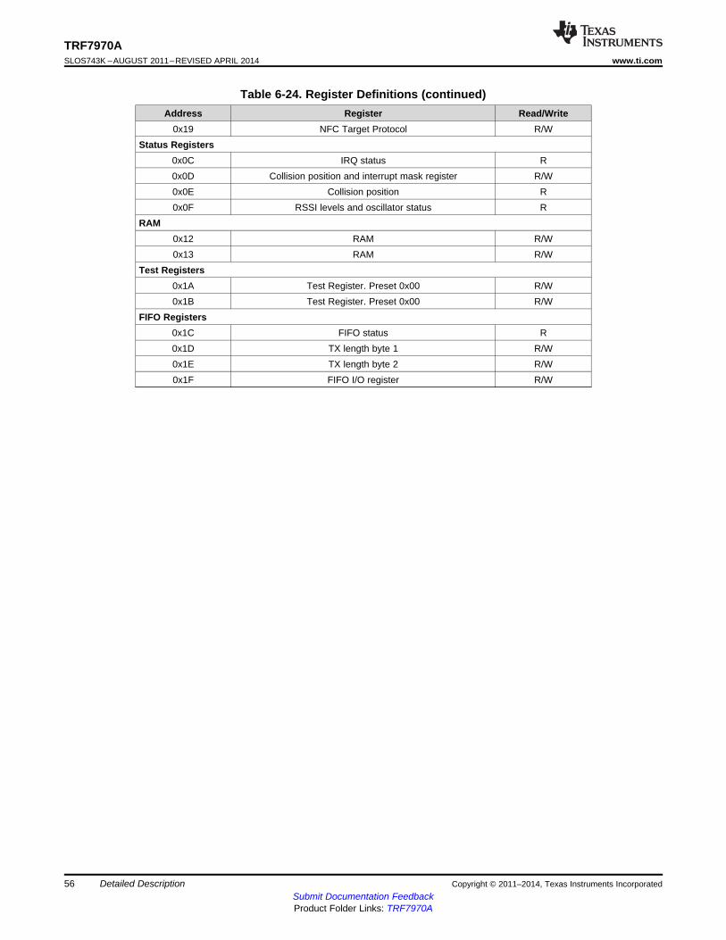
TRF7970ASLOS743K –AUGUST 2011–REVISED APRIL 2014 www.ti.com
Table 6-24. Register Definitions (continued)Address Register Read/Write
0x19 NFC Target Protocol R/WStatus Registers
0x0C IRQ status R0x0D Collision position and interrupt mask register R/W0x0E Collision position R0x0F RSSI levels and oscillator status R
RAM0x12 RAM R/W0x13 RAM R/W
Test Registers0x1A Test Register. Preset 0x00 R/W0x1B Test Register. Preset 0x00 R/W
FIFO Registers0x1C FIFO status R0x1D TX length byte 1 R/W0x1E TX length byte 2 R/W0x1F FIFO I/O register R/W
56 Detailed Description Copyright © 2011–2014, Texas Instruments IncorporatedSubmit Documentation FeedbackProduct Folder Links: TRF7970A
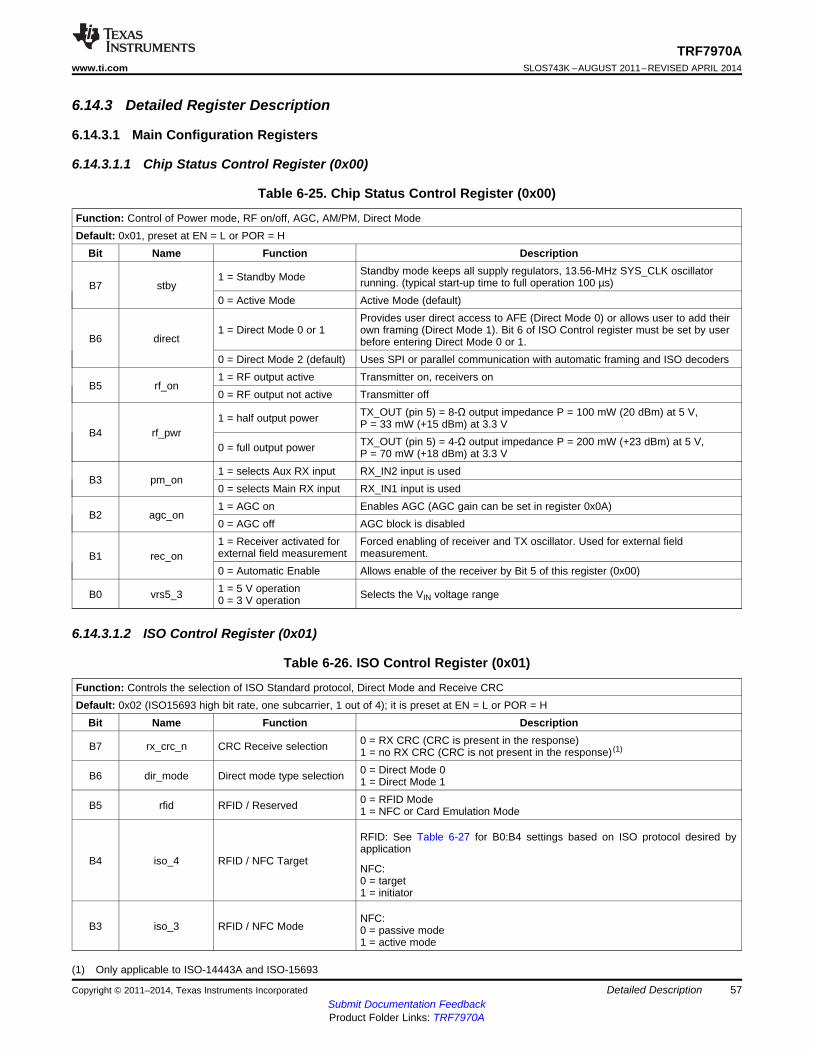
TRF7970Awww.ti.com SLOS743K –AUGUST 2011–REVISED APRIL 2014
6.14.3 Detailed Register Description
6.14.3.1 Main Configuration Registers
6.14.3.1.1 Chip Status Control Register (0x00)
Table 6-25. Chip Status Control Register (0x00)
Function: Control of Power mode, RF on/off, AGC, AM/PM, Direct ModeDefault: 0x01, preset at EN = L or POR = H
Bit Name Function DescriptionStandby mode keeps all supply regulators, 13.56-MHz SYS_CLK oscillator1 = Standby Mode running. (typical start-up time to full operation 100 µs)B7 stby
0 = Active Mode Active Mode (default)Provides user direct access to AFE (Direct Mode 0) or allows user to add their
1 = Direct Mode 0 or 1 own framing (Direct Mode 1). Bit 6 of ISO Control register must be set by userB6 direct before entering Direct Mode 0 or 1.
0 = Direct Mode 2 (default) Uses SPI or parallel communication with automatic framing and ISO decoders1 = RF output active Transmitter on, receivers on
B5 rf_on0 = RF output not active Transmitter off
TX_OUT (pin 5) = 8-Ω output impedance P = 100 mW (20 dBm) at 5 V,1 = half output power P = 33 mW (+15 dBm) at 3.3 VB4 rf_pwr
TX_OUT (pin 5) = 4-Ω output impedance P = 200 mW (+23 dBm) at 5 V,0 = full output power P = 70 mW (+18 dBm) at 3.3 V1 = selects Aux RX input RX_IN2 input is used
B3 pm_on0 = selects Main RX input RX_IN1 input is used1 = AGC on Enables AGC (AGC gain can be set in register 0x0A)
B2 agc_on0 = AGC off AGC block is disabled1 = Receiver activated for Forced enabling of receiver and TX oscillator. Used for external fieldexternal field measurement measurement.B1 rec_on0 = Automatic Enable Allows enable of the receiver by Bit 5 of this register (0x00)1 = 5 V operationB0 vrs5_3 Selects the VIN voltage range0 = 3 V operation
6.14.3.1.2 ISO Control Register (0x01)
Table 6-26. ISO Control Register (0x01)
Function: Controls the selection of ISO Standard protocol, Direct Mode and Receive CRCDefault: 0x02 (ISO15693 high bit rate, one subcarrier, 1 out of 4); it is preset at EN = L or POR = H
Bit Name Function Description0 = RX CRC (CRC is present in the response)B7 rx_crc_n CRC Receive selection 1 = no RX CRC (CRC is not present in the response) (1)
0 = Direct Mode 0B6 dir_mode Direct mode type selection 1 = Direct Mode 10 = RFID ModeB5 rfid RFID / Reserved 1 = NFC or Card Emulation Mode
RFID: See Table 6-27 for B0:B4 settings based on ISO protocol desired byapplication
B4 iso_4 RFID / NFC TargetNFC:0 = target1 = initiator
NFC:B3 iso_3 RFID / NFC Mode 0 = passive mode
1 = active mode
(1) Only applicable to ISO-14443A and ISO-15693
Copyright © 2011–2014, Texas Instruments Incorporated Detailed Description 57Submit Documentation FeedbackProduct Folder Links: TRF7970A

TRF7970ASLOS743K –AUGUST 2011–REVISED APRIL 2014 www.ti.com
Table 6-26. ISO Control Register (0x01) (continued)
NFC:B2 iso_2 RFID / Card Emulation 0 = NFC Normal Modes
1 = Card Emulation Mode
NFC:B1 iso_1 RFID / NFC bit rate0 = bit rate selection or card emulation selection, see Table 6-28
NFC:B0 iso_0 RFID / NFC bit rate0 = bit rate selection or card emulation selection, see Table 6-28
Table 6-27. ISO Control Register ISO_x Settings, RFID Mode
ISO_4 ISO_3 ISO_2 ISO_1 ISO_0 Protocol Remarks0 0 0 0 0 ISO15693 low bit rate, 6.62 kbps, one subcarrier, 1 out of 40 0 0 0 1 ISO15693 low bit rate, 6.62 kbps, one subcarrier, 1 out of 2560 0 0 1 0 ISO15693 high bit rate, 26.48 kbps, one subcarrier, 1 out of 4 Default for reader0 0 0 1 1 ISO15693 high bit rate, 26.48 kbps, one subcarrier, 1 out of 2560 0 1 0 0 ISO15693 low bit rate, 6.67 kbps, double subcarrier, 1 out of 40 0 1 0 1 ISO15693 low bit rate, 6.67 kbps, double subcarrier, 1 out of 2560 0 1 1 0 ISO15693 high bit rate, 26.69 kbps, double subcarrier, 1 out of 4
ISO15693 high bit rate, 26.69 kbps, double subcarrier,0 0 1 1 1 1 out of 2560 1 0 0 0 ISO14443A RX bit rate, 106 kbps RX bit rate (1)
0 1 0 0 1 ISO14443A RX high bit rate, 212 kbps0 1 0 1 0 ISO14443A RX high bit rate, 424 kbps0 1 0 1 1 ISO14443A RX high bit rate, 848 kbps0 1 1 0 0 ISO14443B RX bit rate, 106 kbps RX bit rate (1)
0 1 1 0 1 ISO14443B RX high bit rate, 212 kbps0 1 1 1 0 ISO14443B RX high bit rate, 424 kbps0 1 1 1 1 ISO14443B RX high bit rate, 848 kbps1 0 0 1 1 Reserved1 0 1 0 0 Reserved1 1 0 1 0 FeliCa 212 kbps1 1 0 1 1 FeliCa 424 kbps
(1) For ISO14443A/B, when bit rate of TX is different from RX, settings can be done in register 0x02 or 0x03.
Table 6-28. ISO Control Register ISO_x Settings,NFC Mode (B5 = 1, B2 = 0) or Card Emulation (B5 = 1, B2 = 1)
NFC Card EmulationISO_1 ISO_0 (B5 = 1, B2 = 0) (B5 = 1, B2 = 1)0 0 N/A ISO14443A0 1 106 kbps ISO14443B1 0 212 kbps N/A1 1 424 kbps N/A
58 Detailed Description Copyright © 2011–2014, Texas Instruments IncorporatedSubmit Documentation FeedbackProduct Folder Links: TRF7970A

TRF7970Awww.ti.com SLOS743K –AUGUST 2011–REVISED APRIL 2014
6.14.3.2 Control Registers – Sub Level Configuration Registers
6.14.3.2.1 ISO14443 TX Options Register (0x02)
Table 6-29. ISO14443 TX Options Register (0x02)
Function: Selects the ISO subsets for ISO14443 – TXDefault: 0x00 at POR = H or EN = L
Bit Name Function DescriptionB7 egt2 TX EGT time select MSB
Three bit code defines the number of etu (0-7) which separate two characters.B6 egt1 TX EGT time select ISO14443B TX only.B5 egt0 TX EGT time select LSB
1 = EOF→ 0 length 11 etuB4 eof_l0 0 = EOF→ 0 length 10 etu1 = SOF→ 1 length 03 etuB3 sof_l1 0 = SOF→ 1 length 02 etu
ISO14443B TX only1 = SOF→ 0 length 11 etuB2 sof _l0 0 = SOF→ 0 length 10 etu1 = EGT after each byte
B1 l_egt 0 = EGT after last byte isomitted1 = ISO14443A Layer 4compliant (in SAK For use with Auto SDD configuration, makes B6 in ISO14443A response 1 or 0,B0 Auto SDD_SAK response) indicating Layer 4 compliance (or not), for all other cases, this bit is unused0 = Not Layer 4 compliant(in SAK response)
6.14.3.2.2 ISO14443 High-Bit-Rate and Parity Options Register (0x03)
Table 6-30. ISO14443 High-Bit-Rate and Parity Options Register (0x03)
Function: Selects the ISO subsets for ISO14443 – TXDefault: 0x00 at POR = H or EN = L, and at each write to ISO Control register
Bit Name Function DescriptionTX bit rate different from RXB7 dif_tx_br Valid for ISO14443A/B high bit ratebit rate enable
B6 tx_br1 tx_br1 = 0, tx_br = 0 → 106 kbpstx_br1 = 0, tx_br = 1 → 212 kbpsTX bit rate tx_br1 = 1, tx_br = 0 → 424 kbpsB5 tx_br0tx_br1 = 1, tx_br = 1 → 848 kbps
1 = parity odd except lastB4 parity-2tx byte which is even for TXFor 14443A high bit rate, coding and decoding
1 = parity odd except lastB3 parity-2rx byte which is even for RXB2 UnusedB1 UnusedB0 Unused
Copyright © 2011–2014, Texas Instruments Incorporated Detailed Description 59Submit Documentation FeedbackProduct Folder Links: TRF7970A

TRF7970ASLOS743K –AUGUST 2011–REVISED APRIL 2014 www.ti.com
6.14.3.2.3 TX Timer High Byte Control Register (0x04)
Table 6-31. TX Timer High Byte Control Register (0x04)
Function: For TimingsDefault: 0xC2 at POR = H or EN = L, and at each write to ISO Control register
Bit Name Function DescriptionB7 tm_st1 Timer Start Condition tm_st1 = 0, tm_st0 = 0 → beginning of TX SOF
tm_st1 = 0, tm_st0 = 1 → end of TX SOFtm_st1 = 1, tm_st0 = 0 → beginning of RX SOFB6 tm_st0 Timer Start Conditiontm_st1 = 1, tm_st0 = 1 → end of RX SOF
B5 tm_lengthD Timer Length MSBB4 tm_lengthC Timer LengthB3 tm_lengthB Timer LengthB2 tm_lengthA Timer LengthB1 tm_length9 Timer LengthB0 tm_length8 Timer Length LSB
6.14.3.2.4 TX Timer Low Byte Control Register (0x05)
Table 6-32. TX Timer Low Byte Control Register (0x05)
Function: For TimingsDefault: 0x00 at POR = H or EN = L, and at each write to ISO Control register
Bit Name Function DescriptionB7 tm_length7 Timer Length MSBB6 tm_length6 Timer Length
Defines the time when delayed transmission is started.B5 tm_length5 Timer Length
RX wait range is 590 ns to 9.76 ms (1 to 16383)B4 tm_length4 Timer Length
Step size is 590 nsB3 tm_length3 Timer LengthAll bits low = timer disabled (0x00)B2 tm_length2 Timer Length
B1 tm_length1 Timer Length Preset 0x00 for all other protocolsB0 tm_length0 Timer Length LSB
60 Detailed Description Copyright © 2011–2014, Texas Instruments IncorporatedSubmit Documentation FeedbackProduct Folder Links: TRF7970A

TRF7970Awww.ti.com SLOS743K –AUGUST 2011–REVISED APRIL 2014
6.14.3.2.5 TX Pulse Length Control Register (0x06)
The length of the modulation pulse is defined by the protocol selected in the ISO Control register 0x01.With a high Q antenna, the modulation pulse is typically prolonged, and the tag detects a longer pulsethan intended. For such cases, the modulation pulse length can be corrected by using the TX PulseLength Control register (0x06). If the register contains all zeros, then the pulse length is governed by theprotocol selection. If the register contains a value other than 0x00, the pulse length is equal to the value ofthe register in 73.7-ns increments. This means the range of adjustment can be 73.7 ns to 18.8 µs.
Table 6-33. TX Pulse Length Control Register (0x06)
Function: Controls the length of TX pulseDefault: 0x00 at POR = H or EN = L and at each write to ISO Control register.
Bit Name Function DescriptionB7 Pul_p2 Pulse length MSB
The pulse range is 73.7 ns to 18.8 µs (1….255), step size 73.7 ns.B6 Pul_p1
All bits low (00): pulse length control is disabled.B5 Pul_p0
The following default timings are preset by the ISO Control register (0x01):B4 Pul_c49.44 µs → ISO15693 (TI Tag-It HF-I)B3 Pul_c3
B2 Pul_c2 11 µs → ReservedB1 Pul_c1 2.36 µs → ISO14443A at 106 kbps
1.4 µs → ISO14443A at 212 kbpsB0 Pul_c0 Pulse length LSB 737 ns → ISO14443A at 424 kbps
442 ns → ISO14443A at 848 kbps; pulse length control disabled
6.14.3.2.6 RX No Response Wait Time Register (0x07)
The RX No Response timer is controlled by the RX NO Response Wait Time Register 0x07. This timermeasures the time from the start of slot in the anticollision sequence until the start of tag response. If thereis no tag response in the defined time, an interrupt request is sent and a flag is set in IRQ status controlregister 0x0C. This enables the external controller to be relieved of the task of detecting empty slots. Thewait time is stored in the register in increments of 37.76 µs. This register is also preset, automatically, forevery new protocol selection. Sending a Reset FIFO (0x0F) direct command after a TX Complete interruptwill disable this feature.
Table 6-34. RX No Response Wait Time Register (0x07)
Function: Defines the time when "no response" interrupt is sent; only for ISO15693Default: 0x0E at POR = H or EN = L and at each write to ISO Control register
Bit Name Function DescriptionB7 NoResp7 No response MSB
Defines the time when "no response" interrupt is sent. It starts from the end ofB6 NoResp6 TX EOF. RX no response wait range is 37.76 µs to 9628 µs (1 to 255), step
size is: 37.76 µs.B5 NoResp5The following default timings are preset by the ISO Control register (0x01):B4 NoResp4
B3 NoResp3 390 µs → ReservedB2 NoResp2 529 µs → for all protocols supported, but not listed hereB1 NoResp1 604 µs → Reserved
755 µs → ISO15693 high data rate (TI Tag-It HF-I)B0 NoResp0 No response LSB1812 µs → ISO15693 low data rate (TI Tag-It HF-I)
Copyright © 2011–2014, Texas Instruments Incorporated Detailed Description 61Submit Documentation FeedbackProduct Folder Links: TRF7970A

TRF7970ASLOS743K –AUGUST 2011–REVISED APRIL 2014 www.ti.com
6.14.3.2.7 RX Wait Time Register (0x08)
The RX-wait-time timer is controlled by the value in the RX wait time register 0x08. This timer defines thetime after the end of the transmit operation in which the receive decoders are not active (held in resetstate). This prevents incorrect detections resulting from transients following the transmit operation. Thevalue of the RX wait time register defines this time in increments of 9.44 µs. This register is preset atevery write to ISO Control register 0x01 according to the minimum tag response time defined by eachstandard.
Table 6-35. RX Wait Time Register (0x08)
Function: Defines the time after TX EOF when the RX input is disregarded for example, to block out electromagnetic disturbancegenerated by the responding card.Default: 0x1F at POR = H or EN = L and at each write toISO control register.
Bit Name Function DescriptionB7 Rxw7
Defines the time after the TX EOF during which the RX input is ignored. TimeB6 Rxw6 starts from the end of TX EOF.B5 Rxw5 RX wait range is 9.44 µs to 2407 µs (1 to 255), Step size 9.44 µs.B4 Rxw4
The following default timings are preset by the ISO Control register (0x01):RX wait timeB3 Rxw3
9.44 µs → FeliCaB2 Rxw2
66 µs → ISO14443A and BB1 Rxw1180 µs → Reserved
B1 Rxw0293 µs → ISO15693 (TI Tag-It HF-I)
62 Detailed Description Copyright © 2011–2014, Texas Instruments IncorporatedSubmit Documentation FeedbackProduct Folder Links: TRF7970A

TRF7970Awww.ti.com SLOS743K –AUGUST 2011–REVISED APRIL 2014
6.14.3.2.8 Modulator and SYS_CLK Control Register (0x09)
The frequency of SYS_CLK (pin 27) is programmable by the bits B4 and B5 of this register. The frequencyof the TRF7970A system clock oscillator is divided by 1, 2 or 4 resulting in available SYS_CLKfrequencies of 13.56 MHz or 6.78 MHz or 3.39 MHz.
The ASK modulation depth is controlled by bits B0, B1 and B2. The range of ASK modulation is 7% to30% or 100% (OOK). The selection between ASK and OOK (100%) modulation can also be done usingdirect input OOK (pin 12). The direct control of OOK/ASK using OOK pin is only possible if the function isenabled by setting B6 = 1 (en_ook_p) in this register (0x09) and the ISO Control Register (0x01, B6 = 1).When configured this way, the MOD (pin 14) is used as input for the modulation signal.
Table 6-36. Modulator and SYS_CLK Control Register (0x09)
Function: Controls the modulation input and depth, ASK / OOK control and clock output to external system (MCU)Default: 0x91 at POR = H or EN = L, and at each write to ISO control register, except Clo1 and Clo0.
Bit Name Function DescriptionB7 27MHz Enables 27.12-MHz crystal Default = 1 (enabled)
Enable ASK/OOK pin (pin 12) for "on the fly change" between any preselected1 = Enables external ASK modulation as defined by B0 to B2 and OOK modulation:selection of ASK or OOK
B6 en_ook_p modulation If B6 is 1, pin 12 is configured as follows:0 = Default operation as
1 = OOK modulationdefined in B0 to B2 (0x09)0 = Modulation as defined in B0 to B2 (0x09)
SYS_CLK Output SYS_CLK OutputClo1 Clo0 (if 13.56-MHz (if 27.12-MHz
SYS_CLK output frequency crystal is used) crystal is used)B5 Clo1 MSB 0 0 Disabled Disabled0 1 3.39 MHz 6.78 MHz1 0 6.78 MHz 13.56 MHzSYS_CLK output frequencyB4 Clo0 LSB 1 1 13.56 MHz 27.12 MHz
1 = Sets pin 12 (ASK/OOK) For test and measurement purpose. ASK/OOK pin 12 can be used to monitorB3 en_ana as an analog output the analog subcarrier signal before the digitizing with DC level equal to AGND.0 = DefaultPm2 Pm1 Pm0 Mod Type and %
B2 Pm2 Modulation depth MSB 0 0 0 ASK 10%0 0 1 OOK (100%)0 1 0 ASK 7%
B1 Pm1 Modulation depth 0 1 1 ASK 8.5%1 0 0 ASK 13%1 0 1 ASK 16%
B0 Pm0 Modulation depth LSB 1 1 0 ASK 22%1 1 1 ASK 30%
Copyright © 2011–2014, Texas Instruments Incorporated Detailed Description 63Submit Documentation FeedbackProduct Folder Links: TRF7970A

TRF7970ASLOS743K –AUGUST 2011–REVISED APRIL 2014 www.ti.com
6.14.3.2.9 RX Special Setting Register (Address 0x0A)
Table 6-37. RX Special Setting Register (Address 0x0A)
Function: Sets the gains and filters directlyDefault: 0x40 at POR = H or EN = L, and at each write to the ISO Control register 0x01. When bits B7, B6, B5 and B4 are all zero, thefilters are set for ISO14443B (240 kHz to 1.4 MHz).
Bit Name Function DescriptionB7 C212 Bandpass 110 kHz to 570 kHz Appropriate for 212-kHz subcarrier system (FeliCa)B6 C424 Bandpass 200 kHz to 900 kHz Appropriate for 424-kHz subcarrier used in ISO15693
Appropriate for Manchester-coded 848-kHz subcarrier used in ISO14443AB5 M848 Bandpass 450 kHz to 1.5 MHz and BBandpass 100 kHz to 1.5 MHzB4 hbt Appropriate for highest bit rate (848 kbps) used in high-bit-rate ISO14443Gain reduced for 18 dB
B3 gd1 00 = Gain reduction 0 dB01 = Gain reduction for 5 dB Sets the RX gain reduction, and reduces sensitivity10 = Gain reduction for 10 dBB2 gd211 = Gain reduction for 15 dB
AGC activation level changed from five times the digitizing level to threetimes the digitizing level.B1 agcr AGC activation level change 1 = 3x0 = 5xAGC action can be done any time during receive process. It is not limitedto the start of receive ("max hold").B0 no-lim AGC action is not limited in time 1 = continuously – no time limit0 = 8 subcarrier pulses
The first four steps of the AGC control are comparator adjustment. The second three steps are real gainreduction done automatically by AGC control. The AGC is turned on after TX.
The first gain and filtering stage following the RF envelope detector has a nominal gain of 15 and the 3-dBband-pass frequencies are adjustable in the range from 100 kHz to 400 kHz for high pass and 600 kHz to1.5 MHz for low pass. The next gain and filtering stage has a nominal gain of 8 and the frequencycharacteristic identical to first stage. The filter setting is done automatically with internal preset for eachnew selection of communication standard in ISO Control register (0x01). Additional corrections can bedone by directly writing into the RX Special Setting register 0x0A.
The second receiver gain stage and digitizer stage are included in the AGC loop. The AGC loop can beactivated by setting the bit B2 = 1 (agc-on) in Chip Status Control register 0x00. If activated the AGCmonitors the signal level at the input of digitizing stage. If the signal level is significantly higher than thedigitizing threshold level, the gain reduction is activated. The signal level, at which the action is started, isby default five times the digitizing threshold level. It can be reduced to three times the digitizing level bysetting bit B1 = 1 (agcr) in RX Special Setting register (0x0A).
The AGC action is fast and it typically finishes within eight subcarrier pulses. By default the AGC action isblocked after first few pulses of subcarrier signal so AGC cannot interfere with signal reception during restof data packet. In certain cases, this is not optimal, so this blocking can be removed by setting B0 = 1(no_lim) in RX Special Setting register (0x0A).
NOTEThe setting of bits B4, B5, B6 and B7 to zero selects bandpass characteristic of 240 kHz to1.4 MHz. This is appropriate for ISO14443B, FeliCa protocol, and ISO14443A higher bitrates 212 kbps and 424 kbps.
64 Detailed Description Copyright © 2011–2014, Texas Instruments IncorporatedSubmit Documentation FeedbackProduct Folder Links: TRF7970A

TRF7970Awww.ti.com SLOS743K –AUGUST 2011–REVISED APRIL 2014
6.14.3.2.10 Regulator and I/O Control Register (0x0B)
Table 6-38. Regulator and I/O Control Register (0x0B)
Function: Control the three voltage regulatorsDefault: 0x87 at POR = H or EN = L
Bit Name Function Description0 = Manual settings; see B0to B2 in Table 6-39 and Auto system sets VDD_RF = VIN – 250 mV and VDD_A = VIN – 250 mV andB7 auto_reg Table 6-40 VDD_X= VIN – 250 mV, but not higher than 3.4 V.1 = Automatic setting
Internal peak detectors are disabled, receiver inputs (RX_IN1 and RX_IN2)Support for external powerB6 en_ext_pa accept externally demodulated subcarrier. At the same time ASK/OOK pin 12amplifier becomes modulation output for external TX amplifier.When B5 = 1, maintains the output driving capabilities of the I/O pins connected1 = enable low peripheralB5 io_low to the level shifter under low voltage operation. Should be set 1 when VDD_I/Ocommunication voltage voltage is between 1.8 V to 2.7 V.
B4 Unused No function Default is 0.B3 Unused No function Default is 0.B2 vrs2
Voltage set MSB voltage Vrs3_5 = L: VDD_RF, VDD_A, VDD_X range 2.7 V to 3.4 V; see Table 6-39 andB1 vrs1 set LSB Table 6-40B0 vrs0
Table 6-39. Supply-Regulator Setting – Manual 5-V System
Option Bits Setting in Control RegisterRegister Action
B7 B6 B5 B4 B3 B2 B1 B000 1 5-V system0B 0 Manual regulator setting0B 0 1 1 1 VDD_RF = 5 V, VDD_A = 3.4 V, VDD_X = 3.4 V0B 0 1 1 0 VDD_RF = 4.9 V, VDD_A = 3.4 V, VDD_X = 3.4 V0B 0 1 0 1 VDD_RF = 4.8 V, VDD_A = 3.4 V, VDD_X = 3.4 V0B 0 1 0 0 VDD_RF = 4.7 V, VDD_A = 3.4 V, VDD_X = 3.4 V0B 0 0 1 1 VDD_RF = 4.6 V, VDD_A = 3.4 V, VDD_X = 3.4 V0B 0 0 1 0 VDD_RF = 4.5 V, VDD_A = 3.4 V, VDD_X = 3.4 V0B 0 0 0 1 VDD_RF = 4.4 V, VDD_A = 3.4 V, VDD_X = 3.4 V0B 0 0 0 0 VDD_RF = 4.3 V, VDD_A = 3.4 V, VDD_X = 3.4 V
Table 6-40. Supply-Regulator Setting – Manual 3-V System
Option Bits Setting in Control RegisterRegister Action
B7 B6 B5 B4 B3 B2 B1 B000 0 3-V system0B 0 Manual regulator setting0B 0 1 1 1 VDD_RF = 3.4 V, VDD_A and VDD_X = 3.4 V0B 0 1 1 0 VDD_RF = 3.3 V, VDD_A and VDD_X = 3.3 V0B 0 1 0 1 VDD_RF = 3.2 V, VDD_A and VDD_X = 3.2 V0B 0 1 0 0 VDD_RF = 3.1 V, VDD_A and VDD_X = 3.1 V0B 0 0 1 1 VDD_RF = 3.0 V, VDD_A and VDD_X = 3.0 V0B 0 0 1 0 VDD_RF = 2.9 V, VDD_A and VDD_X = 2.9 V0B 0 0 0 1 VDD_RF = 2.8 V, VDD_A and VDD_X = 2.8 V0B 0 0 0 0 VDD_RF = 2.7 V, VDD_A and VDD_X = 2.7 V
Copyright © 2011–2014, Texas Instruments Incorporated Detailed Description 65Submit Documentation FeedbackProduct Folder Links: TRF7970A

TRF7970ASLOS743K –AUGUST 2011–REVISED APRIL 2014 www.ti.com
Table 6-41. Supply-Regulator Setting – Automatic 5-V System
Option Bits Setting in Control RegisterRegister Action
B7 B6 B5 B4 B3 B2 B1 B000 1 5-V system0B 1 x (1) 0 0 Automatic regulator setting 400-mV difference
(1) x = don't care
Table 6-42. Supply-Regulator Setting – Automatic 3-V System
Option Bits Setting in Control RegisterRegister Action
B7 B6 B5 B4 B3 B2 B1 B000 0 3-V system0B 1 x (1) 0 0 Automatic regulator setting 400-mV difference
(1) x = don't care
6.14.3.3 Status Registers
6.14.3.3.1 IRQ Status Register (0x0C)
Table 6-43. IRQ Status Register (0x0C)
Function: Information available about TRF7970A IRQ and TX/RX statusDefault: 0x00 at POR = H or EN = L, and at each write to the ISO Control Register 0x01. It is also automatically reset at the end of a readphase. The reset also removes the IRQ flag.
Bit Name Function DescriptionSignals that TX is in progress. The flag is set at the start of TX but the interruptB7 Irq_tx IRQ set due to end of TX request (IRQ = 1) is sent when TX is finished.Signals that RX SOF was received and RX is in progress. The flag is set at theB6 Irg_srx IRQ set due to RX start start of RX but the interrupt request (IRQ = 1) is sent when RX is finished.Signals FIFO high or low as set in the Adjustable FIFO IRQ Levels (0x14)B5 Irq_fifo Signals the FIFO level registerIndicates receive CRC error only if B7 (no RX CRC) of ISO Control register isB4 Irq_err1 CRC error set to 0.
B3 Irq_err2 Parity error Indicates parity error for ISO14443AB2 Irq_err3 Byte framing or EOF error Indicates framing error
Collision error for ISO14443A and ISO15693 single subcarrier. Bit is set if morethen 6 or 7 (as defined in register 0x01) are detected inside one bit period ofB1 Irq_col Collision error ISO14443A 106 kbps. Collision error bit can also be triggered by externalnoise.No response within the "No-response time" defined in RX No-response Wait
B0 Irq_noresp No-response time interrupt Time register (0x07). Signals the MCU that next slot command can be sent.Only for ISO15693.
To reset (clear) the register 0x0C and the IRQ line, the register must be read. During Transmit thedecoder is disabled, only bits B5 and B7 can be changed. During Receive only bit B6 can be changed, butdoes not trigger the IRQ line immediately. The IRQ signal is set at the end of Transmit and Receivephase.
66 Detailed Description Copyright © 2011–2014, Texas Instruments IncorporatedSubmit Documentation FeedbackProduct Folder Links: TRF7970A

TRF7970Awww.ti.com SLOS743K –AUGUST 2011–REVISED APRIL 2014
Table 6-44. IRQ Status Register (0x0C) for NFC and Card Emulation Operation
Function: Information available about TRF7970A IRQ and TX/RX statusDefault: 0x00 at POR = H or EN = L, and at each write to the ISO Control Register 0x01. It is also automatically reset at the end of a readphase. The reset also removes the IRQ flag.
Bit Name Function DescriptionSignals that TX is in progress. The flag is set at the start of TX but the interruptB7 Irq_tx IRQ set due to end of TX request (IRQ = 1) is sent when TX is finished.Signals that RX SOF was received and RX is in progress. The flag is set at theB6 Irg_srx IRQ set due to RX start start of RX but the interrupt request (IRQ = 1) is sent when RX is finished.Signals FIFO high or low as set in the Adjustable FIFO IRQ Levels (0x14)B5 Irq_fifo Signals the FIFO level register
B4 Irq_err1 Protocol error Any protocol errorB3 Irq_sdd SDD completed SDD (passive target at 106 kbps) successfully finishedB2 Irq_rf RF field change Sufficient RF signal level for operation was reached or lost
RF collision avoidance The system has finished collision avoidance and the minimum wait time isB1 Irq_col finished elapsed.RF collision avoidance not The external RF field was present so the collision avoidance could not beB0 Irq_col_err finished successfully carried out.
6.14.3.3.2 Interrupt Mask Register (0x0D) and Collision Position Register (0x0E)
Table 6-45. Interrupt Mask Register (0x0D)
Default: 0x3E at POR = H and EN = L. Collision bits reset automatically after read operation.Bit Name Function DescriptionB7 Col9 Bit position of collision MSB Supports ISO14443AB6 Col8 Bit position of collisionB5 En_irq_fifo Interrupt enable for FIFO Default = 1B4 En_irq_err1 Interrupt enable for CRC Default = 1B3 En_irq_err2 Interrupt enable for Parity Default = 1
Interrupt enable for FramingB2 En_irq_err3 Default = 1error or EOFInterrupt enable for collisionB1 En_irq_col Default = 1errorEnables no-responseB0 En_irq_noresp Default = 0interrupt
Table 6-46. Collision Position Register (0x0E)
Function: Displays the bit position of collision or errorDefault: 0x00 at POR = H and EN = L. Automatically reset after read operation.
Bit Name Function DescriptionB7 Col7 Bit position of collision MSBB6 Col6B5 Col5B4 Col4 ISO14443A mainly supported, in the other protocols this register shows the bit
position of error. Either frame, SOF/EOF, parity or CRC error.B3 Col3B2 Col2B1 Col1B0 Col0 Bit position of collision LSB
Copyright © 2011–2014, Texas Instruments Incorporated Detailed Description 67Submit Documentation FeedbackProduct Folder Links: TRF7970A

TRF7970ASLOS743K –AUGUST 2011–REVISED APRIL 2014 www.ti.com
6.14.3.3.3 RSSI Levels and Oscillator Status Register (0x0F)
Table 6-47. RSSI Levels and Oscillator Status Register (0x0F)
Function: Displays the signal strength on both reception channels and RF amplitude during RF-off state. The RSSI values are valid fromreception start till start of next transmission.
Bit Name Function DescriptionB7 Unused
Crystal oscillator stableB6 osc_ok 13.56-MHz frequency stable (≈200 µs)indicatorMSB RSSI value of auxiliaryB5 rssi_x2 Auxiliary channel is by default RX_IN2. The input can be swapped by B3 = 1RX (RX_IN2)
(Chip State Control register 0x00). If "swapped", the Auxiliary channel isB4 rssi_x1 Auxiliary channel RSSI connected to RX_IN1 and, hence, the Auxiliary RSSI represents the signal levelMSB RSSI value of auxiliary at RX_IN2.B3 rssi_x0 RX (RX_IN2)MSB RSSI value of mainB2 rssi_2 RX (RX_IN1)
Active channel is default and can be set with option bit B3 = 0 of chip stateB1 rssi_1 Main channel RSSI control register 0x00.LSB RSSI value of main RXB0 rssi_0 (RX_IN1)
RSSI measurement block is measuring the demodulated envelope signal (except in case of directcommand for RF amplitude measurement described later in direct commands section). The measuringsystem is latching the peak value, so the RSSI level can be read after the end of receive packet. TheRSSI value is reset during next transmit action of the reader, so the new tag response level can bemeasured. The RSSI levels calculated to the RF_IN1 and RF_IN2 are presented in Section 6.5.1.1 andSection 6.5.1.2. The RSSI has 7 steps (3 bits) with 4-dB increment. The input level is the peak to peakmodulation level of RF signal measured on one side envelope (positive or negative).
6.14.3.3.4 Special Functions Register (0x10)
Table 6-48. Special Functions Register (0x10)
Function: User configurable options for ISO14443A specific operationsBit Name Function DescriptionB7 Reserved ReservedB6 Reserved Reserved
Disables parity checking forB5 par43 ISO14443A0 = 18.88 µsB4 next_slot_37us Sets the time grid for next slot command in ISO156931 = 37.77 µsBit stream transmit for Enables direct mode for transmitting ISO14443A data, bypassing the FIFO andB3 Sp_dir_mode MIFARE at 106 kbps feeding the data bit stream directly onto the encoder.0 = normal receive Enable 4-bit replay for example, ACK, NACK used by some cards; for example,B2 4_bit_RX 1 = 4-bit receive MIFARE Ultralight0 = anticollision framing(0x93, 0x95, 0x97) Disable anticollision frames for 14443A (this bit should be set to 1 afterB1 14_anticoll 1 = normal framing (no anticollision is finished)broken bytes)0 = 7 subcarrier pulses Selects the number of subcarrier pulses that trigger collision error in theB0 col_7_6 1 = 6 subcarrier pulses 14443A - 106 kbps
68 Detailed Description Copyright © 2011–2014, Texas Instruments IncorporatedSubmit Documentation FeedbackProduct Folder Links: TRF7970A

TRF7970Awww.ti.com SLOS743K –AUGUST 2011–REVISED APRIL 2014
6.14.3.3.5 Special Functions Register (0x11)
Table 6-49. Special Functions Register (0x11)
Function: Indicate IRQ status for RX operations.Bit Name Function DescriptionB7 Reserved ReservedB6 Reserved ReservedB5 Reserved ReservedB4 Reserved ReservedB3 Reserved ReservedB2 Reserved ReservedB1 Reserved Reserved
Copy of the RX start signal Signals the RX SOF was received and the RX is in progress. IRQ when RX isB0 irg_srx (Bit 6) of the IRQ Status completed.Register (0x0C)
6.14.3.3.6 Adjustable FIFO IRQ Levels Register (0x14)
Table 6-50. Adjustable FIFO IRQ Levels Register (0x14)
Function: Adjusts level at which FIFO indicates status by IRQDefault: 0x00 at POR = H and EN = L
Bit Name Function DescriptionB7 Reserved ReservedB6 Reserved ReservedB5 Reserved ReservedB4 Reserved ReservedB3 Wlh_1 Wlh_1 Wlh_0 IRQ Level
0 0 124FIFO high IRQ level (during 0 1 120RX)B2 Wlh_0 1 0 1121 1 96
B1 Wll_1 Wll_1 Wll_0 IRQ Level0 0 4FIFO low IRQ level (during 0 1 8TX)B0 Wll_0 1 0 161 1 32
6.14.3.3.7 NFC Low Field Level Register (0x16)
Table 6-51. NFC Low Field Level Register (0x16)
Function: Defines level for RF collision avoidanceDefault: 0x00 at POR = H and EN = L.
Bit Name Function DescriptionB7 Clex_dis Disable clock extractor NFC passive 106-kbps and ISO14443A card emulationB6 Hash6 N/AB5 Hash5 N/AB4 Hash4 N/AB3 Hash3 N/AB2 Rfdet_I2
RF field level for RF Comparator output is displayed in B6 of the NFC Target Protocol registerB1 Rfdet_I1 collision avoidance (0x19)B0 Rfdet_I0
Copyright © 2011–2014, Texas Instruments Incorporated Detailed Description 69Submit Documentation FeedbackProduct Folder Links: TRF7970A

TRF7970ASLOS743K –AUGUST 2011–REVISED APRIL 2014 www.ti.com
6.14.3.3.8 NFCID1 Number Register (0x17)
This register is used to hold the ID of the TRF7970A for use during card emulation and NFC peer-to-peertarget operations.
The procedure for writing the ID into register 0x17 is the following:1. Write bits 5, 6, and 7 in register 0x18 to enable SDD anticollision (bit 5), and set bit 6 and 7 to select
the ID length of 4, 7, or 10 bytes.2. Write the ID into register 0x17. This should be done using write continuous mode with 4, 7, or 10 bytes
(according to what was set in register 0x18 bits 6 and 7).
6.14.3.3.9 NFC Target Detection Level Register (0x18)
Table 6-52. NFC Target Detection Level Register (0x18)
Function: Defines level for RF wake up, enables automatic SDD and gives NFCID size. This register is supplied by Vin to ensure dataretention during complete power down.Default: 0x00 at POR on Vin (not POR based on VDD_X) and not reset at EN = 0
Bit Name Function DescriptionNFCID1 SizeId_s1 Id_s0 (bytes)
B7 Id_s1 0 0 4NFCID1 size used in 106-kbps passive target SDD 0 1 7
1 0 10B6 Id_s0
1 1 Not allowedAutomatic SDD using internal state machine and ID stored in the NFCID1B5 Sdd_en Number register (0x17)
B4 N/AExtended range for RFB3 Hi_rf measurements
B2 Rfdet_h2 RF field level required for Comparator output is displayed in B7 of the NFC Target Protocol registersystem wakeup. If all bits (0x19)B1 Rfdet_h1 are 0, then the RF level
B0 Rfdet_h0 detection is off.
70 Detailed Description Copyright © 2011–2014, Texas Instruments IncorporatedSubmit Documentation FeedbackProduct Folder Links: TRF7970A

TRF7970Awww.ti.com SLOS743K –AUGUST 2011–REVISED APRIL 2014
6.14.3.3.10 NFC Target Protocol Register (0x19)
This register is used (when read) to display the bit rate and protocol type when an NFC/RFIDInitiator/Reader is presented. An example use of this scenario would be when the TRF7970A is placedinto card emulation (Type A or Type B) and another TRF7970A or NFC device (polling for other NFCdevices) is presented to the TRF7970A in card emulation mode. The IRQ indicates that a field wasdetected (IRQ Status = 0x04) or that Auto SDD has completed (IRQ Status = 0x08, if configured forAutoSDD).
If Auto SDD is set and 0x04 is returned in IRQ status, then this register can be read out to see whichcommands are coming in for gaining knowledge of the polling cycle sequence. Then, when the correct firstmatching command (that is, REQA or REQB) is issued from Reader or Initiator, if AutoSDD is set, the IRQfires and the IRQ Status is 0x08, indicating completion of the SDD. The next IRQ should return 0x40 asstatus, the Register 0x19 can be checked to make sure it is correct value (that is, 0xC9 for Type A at 106kpbs or 0xC5 for Type B at 106 kbps) indicating there are bytes in the FIFO and a read of the FIFO statusindicates how many bytes to read out. For example, after AutoSDD is completed, there are four bytes inthe FIFO, and these should be the RATS command coming in from the reader, which the MCU controllingthe TRF7970A in Card Emulation mode must respond to. If AutoSDD is not set, as another example withthe TRF7970A in ISO14443B Card Emulation mode, then the field detect happens as previously describedand IRQs also fire to indicate RX is complete (0x40). This register must be checked and compared againstcase statement structure that is set up for the value of this register to be 0xC5, indicating that anISO14443B command at 106 kbps was issued. When this register (0x19) is 0xC5, then the FIFO Statuscan be read and should hold a value of 0x03, and when read, be the REQB command (0x05, 0x00, 0x00);the controlling MCU must respond with the ATQB response. The next steps for either of these examplesfollow the revelent portions of the ISO14443-3 or -4 standards, then the NFC Forum specifications,depending on the system use case or application.
Table 6-53. NFC Target Protocol Register (0x19)
Function: Displays the bit rate and protocol type (active or passive) transmitted by initiator in first command. It also displays the comparatoroutputs of both RF level detectors.Default: 0x00 at POR = H and EN = L. B0 to B4 are automatically reset after MCU continuous read operation. B6 and B7 continuouslydisplay the RF level comparator outputs.
Bit Name Function DescriptionRF level is above the wake- The wakeup level is defined by bits B0 to B2 in the NFC Target Detection LevelB7 Rf_h up level setting register (0x18)RF level is above the RF The collision avoidance level is defined by bits B0 – B2 in the register 0x16B6 Rf_l collision avoidance level (NFC Low Field Detection Level)setting
B5 Reserved Reserved Reserved1 = FeliCaB4 FeliCa The first initiator command had physical level coding of FeliCa or ISO14443A0 = ISO14443APassive target at 106 kbpsB3 Pas_106 The first initiator/reader command was SENS_REQ or ALL_REQor transponder emulationISO14443B transponderB2 Pas_14443B The first reader command was ISO14443Bemulation
B1 NFCBR1 00 = ReservedBit rate of first received 01 = 106 kbpscommand 10 = 212 kbpsB0 NFCBR0
11 = 424 kbps
Copyright © 2011–2014, Texas Instruments Incorporated Detailed Description 71Submit Documentation FeedbackProduct Folder Links: TRF7970A

TRF7970ASLOS743K –AUGUST 2011–REVISED APRIL 2014 www.ti.com
6.14.3.4 Test Registers
6.14.3.4.1 Test Register (0x1A)
Table 6-54. Test Register (0x1A) (for Test or Direct Use)
Default: 0x00 at POR = H and EN = L.Bit Name Function DescriptionB7 OOK_Subc_In Subcarrier Input OOK Pin becomes decoder digital inputB6 MOD_Subc_Out Subcarrier Output MOD Pin becomes receiver digitized subcarrier output
Direct TX modulation andB5 MOD_Direct MOD pin becomes input for TX modulation control by the MCURX reseto_sel = L: First stage output used for analog out and digitizing
B4 o_sel First stage output selectiono_sel = H: Second Stage output used for analog out and digitizing
Second stage gain -6 dB,B3 low2 HP corner frequency/2First stage gain -6 dB, HPB2 low1 corner frequency/2
B1 zun Input followers testAGC test, AGC level isB0 Test_AGC seen on rssi_210 bits
6.14.3.4.2 Test Register 0x1B
Table 6-55. Test Register (0x1B) (for Test or Direct Use)
Default: 0x00 at POR = H and EN = L. When a test_dec or test_io is set IC is switched to test mode. Test Mode persists until a stopcondition arrives. At stop condition the test_dec and test_io bits are cleared.
Bit Name Function DescriptionB7B6
test_rf_level RF level testB5B4B3 test_io1
I/O test Not implementedB2 test_io0B1 test_dec Decoder test modeB0 clock_su Coder clock 13.56 MHz For faster test of coders
72 Detailed Description Copyright © 2011–2014, Texas Instruments IncorporatedSubmit Documentation FeedbackProduct Folder Links: TRF7970A

TRF7970Awww.ti.com SLOS743K –AUGUST 2011–REVISED APRIL 2014
6.14.3.5 FIFO Control Registers
6.14.3.5.1 FIFO Status Register (0x1C)
Table 6-56. FIFO Status Register (0x1C)
Function: Number of bytes available to be read from FIFO (= N number of bytes, in hexadecimal)Bit Name Function DescriptionB7 Foverflow FIFO overflow error Bit is set when FIFO has more than 127 bytes presented to itB6 Fb6 FIFO bytes fb[6]B5 Fb5 FIFO bytes fb[5]B4 Fb4 FIFO bytes fb[4]B3 Fb3 FIFO bytes fb[3]B2 Fb2 FIFO bytes fb[2] Bits B0:B6 indicate how many bytes that are in the FIFO to be read out (= N
number of bytes, in hex)B1 Fb1 FIFO bytes fb[1]B0 Fb0 FIFO bytes fb[0]
Copyright © 2011–2014, Texas Instruments Incorporated Detailed Description 73Submit Documentation FeedbackProduct Folder Links: TRF7970A

TRF7970ASLOS743K –AUGUST 2011–REVISED APRIL 2014 www.ti.com
6.14.3.5.2 TX Length Byte1 Register (0x1D), TX Length Byte2 Register (0x1E)
Table 6-57. TX Length Byte1 Register (0x1D)
Function: High 2 nibbles of complete, intended bytes to be transferred through FIFORegister default is set to 0x00 at POR and EN = 0. It is also automatically reset at TX EOF
Bit Name Function DescriptionNumber of complete byteB7 Txl11 bn[11]Number of complete byteB6 Txl10 bn[10]
High nibble of complete, intended bytes to be transmittedNumber of complete byteB5 Txl9 bn[9]Number of complete byteB4 Txl8 bn[8]Number of complete byteB3 Txl7 bn[7]Number of complete byteB2 Txl6 bn[6]
Middle nibble of complete, intended bytes to be transmittedNumber of complete byteB1 Txl5 bn[5]Number of complete byteB0 Txl4 bn[4]
Table 6-58. TX Length Byte2 Register (0x1E)
Function: Low nibbles of complete bytes to be transferred through FIFO; Information about a broken byte and number of bits to betransferred from itDefault: 0x00 at POR and EN = 0. It is also automatically reset at TX EOF
Bit Name Function DescriptionNumber of complete byteB7 Txl3 bn[3]Number of complete byteB6 Txl2 bn[2]
Low nibble of complete, intended bytes to be transmittedNumber of complete byteB5 Txl1 bn[1]Number of complete byteB4 Txl0 bn[0]Broken byte number of bitsB3 Bb2 bb[2]Broken byte number of bits Number of bits in the last broken byte to be transmitted.B2 Bb1 bb[1] It is taken into account only when broken byte flag is set.Broken byte number of bitsB1 Bb0 bb[0]
B0 Bbf Broken byte flag B0 = 1, indicates that last byte is not complete 8 bits wide.
74 Detailed Description Copyright © 2011–2014, Texas Instruments IncorporatedSubmit Documentation FeedbackProduct Folder Links: TRF7970A

GND
1500pF
1500pF1200pF
1200pF
10pF
680pF100pF 220pF
680pF
150nH330nH
GND
GND
27pF
GND
GNDGND
2.2uF0.01uF
2.2uF0.01uF
GND
GND
2.2uF0.01uF
GND
2.2uF0.01uF
GND
27pF
GND
27pF
GND
1.5uH
68pF
GND
12pF
12pF6.8k
GND
GND
10k
GND
GND
GND
47k
0.1uF
100R
GND
GND
MC-921
GND
0
0
SMA-142-0701-801/806
GND
057-014-2
2.2uF0.01uF
GND
C2
C3
C4
C5
C6
C7C10 C8
C9
L1L2
C11
C16C15
C20C19
C18C17
C22C21
C23C24
L3
C14
C13
C12R1
TCK
TMS
P4.0/TB0
P4.1/TB1
P4.2/TB2
P4.3/TB0
P4.4/TB1
P4.5/TB2
P4.6/TBOUTH/ACLK
P4.7/TBCLK
1
2
3
4
5
6
7
8
9
10
11
12
13
14
28
27
26
25
24
23
22
21 20
19
18
17
16
15
29
30
31
32
33
34
35
36
37
38
TP
39
40
R6
R5
C1
R4
X2
R2
R3
GND12
IN1
GND24
OUT3
X3
VD
D_X
32
OS
C_
IN31
OS
C_
OU
T30
VS
S_D
29
EN
28
SY
S_C
LK
27
DATA
_C
LK
26
EN
225
I/O_724
I/O_623
I/O_522
I/O_421
I/O_320
I/O_219
VDD_A1
VIN2
VDD_PA4
TX_OUT5
VSS_PA6
VDD_RF3
I/O_118
I/0_017
BA
ND
_G
AP
11
VD
D_I/O
16
VS
S_A
15
MO
D14
IRQ
13
AS
K/O
OK
12
VSS_RX7
RX_IN18
VS
S10
RX
_IN
29
GND(PAD)33
X4-1 X4-2
X4-3 X4-4
X4-5 X4-6
X4-7 X4-8
X4-9 X4-10
X4-11 X4-12
X4-13 X4-14
C25C26
SYS_CLK
SY
S_
CL
K
DATA_CLK
DATA
_C
LK
VIN
VIN
IRQ
IRQ
MO
D
MOD
VD
D_
X
VD
D_
X
RST_NMI
RST_NMI
RST_NMI
TCK
TCK
TMS
TMS
TDI
TDI
TDO/TDI
TDO/TDI
VCC
VCC
VCC
VCC
RXDTXD
ASK/OOK
AS
K/O
OK
EN
EN
OSC_OUT
OS
C_
OU
TO
SC
_IN
OSC_IN
JTAG
(+2.7VDC - 5.5VDC)
TRF7970A
TRF7970Awww.ti.com SLOS743K –AUGUST 2011–REVISED APRIL 2014
7 Application Schematic and Layout Considerations
7.1 TRF7970A Reader System Using Parallel Microcontroller Interface
7.1.1 General Application ConsiderationsFigure 7-1 shows the most flexible TRF7970A application schematic. Both ISO15693, ISO14443 andFeliCa systems can be addressed. Due to the low clock frequency on the DATA_CLK line, the parallelinterface is the most robust way to connect the TRF7970A with the MCU.
Figure 7-1 shows matching to a 50-Ω port, which allows connecting to a properly matched 50-Ω antennacircuit or RF measurement equipment (for example, a spectrum analyzer or power meter).
7.1.2 SchematicFigure 7-1 shows a sample application schematic for a parallel MCU interface.
Figure 7-1. Application Schematic – Parallel MCU Interface
An MSP430F2370 (32KB Flash, 2KB RAM) is shown in Figure 7-1. Minimum MCU requirements dependon application requirements and coding style. If only one ISO protocol or a limited command set of aprotocol needs to be supported, MCU Flash and RAM requirements can be significantly reduced. Beaware that recursive inventory and anticollision commands require more RAM than single slottedoperations. For example, current reference firmware for ISO15693 (with host interface) is approximately8KB, using 512B RAM; for all supported protocols (also with same host interface) the reference firmwareis approximately 12KB and uses a minimum of 1KB RAM. An MCU capable of running its GPIOs at13.56 MHz is required for Direct Mode 0 operations.
Copyright © 2011–2014, Texas Instruments Incorporated Application Schematic and Layout Considerations 75Submit Documentation FeedbackProduct Folder Links: TRF7970A

GND
1500pF
1500pF1200pF
1200pF
10pF
680pF100pF 220pF
680pF
150nH330nH
GND
GND
27pF
GND
GNDGND
2.2uF0.01uF2.2uF0.01uF
GNDGND
2.2uF0.01uF
GND
2.2uF0.01uF
GND
27pF
GND
27pF
GND
1.5uH
68pF
GND
12pF
12pF6.8k
GND
GND
10k
GND
GND
47k
0.1uF
100R
GND
GND
MC-921
GND
0
0
SMA-142-0701-801/806
GND
GND
2.2uF0.01uF
GND
057-014-2
C2
C3
C4
C5
C6
C7C10 C8
C9
L1L2
C11
C16C15C20C19
C18C17
C22C21
C23C24
L3
C14
C13
C12R1
TCK
TMS
P4.0/TB0
P4.1/TB1
P4.2/TB2
P4.3/TB0
P4.4/TB1
P4.5/TB2
P4.6/TBOUTH/ACLK
P4.7/TBCLK
1
2
3
4
5
6
7
8
9
10
11
12
13
14
28
27
26
25
24
23
22
21 20
19
18
17
16
15
29
30
31
32
33
34
35
36
37
38
TP
39
40
R6
R5
C1
R4
X2
R2
R3
GND12
IN1
GND24
OUT3
X3
VD
D_X
32
OS
C_
IN31
OS
C_
OU
T30
VS
S_D
29
EN
28
SY
S_C
LK
27
DATA
_C
LK
26
EN
225
I/O_724
I/O_623
I/O_522
I/O_421
I/O_320
I/O_219
VDD_A1
VIN2
VDD_PA4
TX_OUT5
VSS_PA6
VDD_RF3
I/O_118
I/0_017
BA
ND
_G
AP
11
VD
D_I/O
16
VS
S_A
15
MO
D14
IRQ
13
AS
K/O
OK
12
VSS_RX7
RX_IN18
VS
S10
RX
_IN
29
GND(PAD)33
C25C26
X4-1 X4-2
X4-3 X4-4
X4-5 X4-6
X4-7 X4-8
X4-9 X4-10
X4-11 X4-12
X4-13 X4-14
SYS_CLK
SY
S_
CL
K
DATA_CLK
DATA
_C
LK
VIN
VIN
IRQ
IRQ
MO
D
MOD
VD
D_
X
VDD_X
VD
D_
X
RST_NMI
RST_NMI
RST_NMI
TCK
TCK
TMS
TMS
TDI
TDI
TDO/TDI
TDO/TDI
VCC
VCC
VCC
VCC
VCC
RXD
TXD
ASK/OOK
AS
K/O
OK
EN
EN
OSC_OUT
OS
C_
OU
TO
SC
_IN
OSC_IN
P3.0
P3.0
P3.2
P3.2
P3.1
P3.1
P3.6
P3.7
P4.2P4.2
JTAG
(+2.7VDC - 5.5VDC)
TRF7970A
TRF7970ASLOS743K –AUGUST 2011–REVISED APRIL 2014 www.ti.com
7.2 TRF7970A Reader System Using SPI With SS Mode
7.2.1 General Application ConsiderationsFigure 7-2 shows the TRF7970A application schematic optimized for both ISO15693 and ISO14443systems using the Serial Port Interface (SPI). Short SPI lines, proper isolation of radio frequency lines,and a proper ground area are essential to avoid interference. The recommended clock frequency on theDATA_CLK line is 2 MHz.
Figure 7-2 shows matching to a 50-Ω port, which allows connecting to a properly matched 50-Ω antennacircuit or RF measurement equipment (for example, a spectrum analyzer or power meter).
7.2.2 SchematicFigure 7-2 shows a sample application schematic for SPI with an SS mode MCU interface.
Figure 7-2. Application Schematic – SPI With SS Mode MCU Interface
An MSP430F2370 (32KB Flash, 2KB RAM) is shown in Figure 7-2. Minimum MCU requirements dependon application requirements and coding style. If only one ISO protocol or a limited command set of aprotocol needs to be supported, MCU Flash and RAM requirements can be significantly reduced and usershould be aware that recursive inventory and anticollision commands require more RAM than singleslotted operations. For example, current reference firmware for ISO15693 (with host interface) isapproximately 8KB, using 512B RAM and for all supported protocols (also with same host interface) thereference firmware is approximately 12KB and uses a minimum of 1KB RAM. An MCU capable of runningits GPIOs at 13.56 MHz is required for Direct Mode 0 operations.
76 Application Schematic and Layout Considerations Copyright © 2011–2014, Texas Instruments IncorporatedSubmit Documentation FeedbackProduct Folder Links: TRF7970A
TRF7970Awww.ti.com SLOS743K –AUGUST 2011–REVISED APRIL 2014
7.3 Layout ConsiderationsKeep all decoupling capacitors as close to the IC as possible, with the high-frequency decouplingcapacitors (10 nF) closer than the low-frequency decoupling capacitors (2.2 µF).
Place ground vias as close as possible to the ground side of the capacitors and reader IC pins to minimizepossible ground loops.
It is not recommend to use any inductor sizes below 0603, as the output power can be compromised. Ifsmaller inductors are necessary, output performance must be confirmed in the final application.
Pay close attention to the required load capacitance of the crystal, and adjust the two external shuntcapacitors accordingly. Follow the recommendations of the crystal manufacturer for those values.
There should be a common ground plane for the digital and analog sections. The multiple ground sectionsor islands should have vias that tie the different sections of the planes together.
Ensure that the exposed thermal pad at the center of the reader IC is properly laid out. It should be tied toground to help dissipate any heat from the package.
All trace line lengths should be made as short as possible, particularly the RF output path, crystalconnections, and control lines from the reader to the microprocessor. Proper placement of the TRF7970A,microprocessor, crystal, and RF connection or connector help facilitate this.
Avoid crossing of digital lines under RF signal lines. Also, avoid crossing of digital lines with other digitallines when possible. If the crossings are unavoidable, 90° crossings should be used to minimize couplingof the lines.
Depending on the production test plan, consider possible implementations of test pads or test vias for useduring testing. The necessary pads or vias should be placed in accordance with the proposed test plan toenable easy access to those test points.
If the system implementation is complex (for example, if the RFID reader module is a subsystem of agreater system with other modules (Bluetooth, WiFi, microprocessors, and clocks), special considerationsshould be taken to ensure that there is no noise coupling into the supply lines. If needed, special filteringor regulator considerations should be used to minimize or eliminate noise in these systems.
For more information/details on layout considerations, see the TRF796x HF-RFID Reader Layout DesignGuide (SLOA139).
7.4 Impedance Matching TX_Out (Pin 5) to 50 ΩThe output impedance of the TRF7970A when operated at full power out setting is nominally 4 + j0 (4 Ωreal). This impedance must be matched to a resonant circuit and TI recommends matching circuit from4 Ω to 50 Ω, as commercially available test equipment (for example, spectrum analyzers, power meters,and network analyzers) are 50-Ω systems. An impedance-matching reference circuit can be seen inFigure 7-3 and Figure 7-4. This section explains how the values were calculated.
Starting with the 4-Ω source, the process of going from 4 Ω to 50 Ω can be represented on a Smith Chartsimulator (available from http://www.fritz.dellsperger.net/). The elements are combined where appropriate(see Figure 7-3).
Copyright © 2011–2014, Texas Instruments Incorporated Application Schematic and Layout Considerations 77Submit Documentation FeedbackProduct Folder Links: TRF7970A

TRF7970ASLOS743K –AUGUST 2011–REVISED APRIL 2014 www.ti.com
Figure 7-3. Impedance Matching Circuit
This yields the Smith Chart Simulation shown in Figure 7-4.
Figure 7-4. Smith Chart Simulation
78 Application Schematic and Layout Considerations Copyright © 2011–2014, Texas Instruments IncorporatedSubmit Documentation FeedbackProduct Folder Links: TRF7970A

TRF7970Awww.ti.com SLOS743K –AUGUST 2011–REVISED APRIL 2014
Resulting power out can be measured with a power meter or spectrum analyzer with power meter functionor other equipment capable of making a "hot" measurement. Observe maximum power input levels on testequipment and use attenuators whenever available to avoid damage to equipment. Expected outputpower levels under various operating conditions are shown in Table 6-25.
7.5 Reader Antenna Design GuidelinesFor HF antenna design considerations using the TRF7970A, see these documents:• Antenna Matching for the TRF7960 RFID Reader (SLOA135)• TRF7960TB HF RFID Reader Module User's Guide (SLOU297)
Copyright © 2011–2014, Texas Instruments Incorporated Application Schematic and Layout Considerations 79Submit Documentation FeedbackProduct Folder Links: TRF7970A

TRF7970ASLOS743K –AUGUST 2011–REVISED APRIL 2014 www.ti.com
8 Device and Documentation Support
8.1 Documentation SupportThe following documents describe the TRF7970A device. Copies of these documents are available on theInternet at www.ti.com.
SLOZ011 TRF7970A Silicon Errata. Describes the known exceptions to the functional specificationsfor the TRF7970A.
8.2 Community ResourcesThe following links connect to TI community resources. Linked contents are provided "AS IS" by therespective contributors. They do not constitute TI specifications and do not necessarily reflect TI's views;see TI's Terms of Use.
TI E2E Community
TI's Engineer-to-Engineer (E2E) Community. Created to foster collaboration among engineers. Ate2e.ti.com, you can ask questions, share knowledge, explore ideas and help solve problems with fellowengineers.
8.3 TrademarksMSP430 is a trademark of Texas Instruments.ARM is a registered trademark of ARM Limited.Bluetooth is a registered trademark of Bluetooth SIG.MIFARE is a trademark of NXP Semiconductors.FeliCa is a trademark of Sony Corporation.Wi-Fi is a registered trademark of Wi-Fi Alliance.All other trademarks are the property of their respective owners.
8.4 Electrostatic Discharge CautionThis integrated circuit can be damaged by ESD. Texas Instruments recommends that all integrated circuits be handled withappropriate precautions. Failure to observe proper handling and installation procedures can cause damage.
ESD damage can range from subtle performance degradation to complete device failure. Precision integrated circuits may be moresusceptible to damage because very small parametric changes could cause the device not to meet its published specifications.
8.5 GlossarySLYZ022 — TI Glossary.
This glossary lists and explains terms, acronyms and definitions.
9 Mechanical Packaging and Orderable Information
9.1 Packaging InformationThe following pages include mechanical packaging and orderable information. This information is the mostcurrent data available for the designated devices. This data is subject to change without notice andrevision of this document. For browser-based versions of this data sheet, refer to the left-hand navigation.
80 Mechanical Packaging and Orderable Information Copyright © 2011–2014, Texas Instruments IncorporatedSubmit Documentation FeedbackProduct Folder Links: TRF7970A

PACKAGE OPTION ADDENDUM
www.ti.com 4-Apr-2014
Addendum-Page 1
PACKAGING INFORMATION
Orderable Device Status(1)
Package Type PackageDrawing
Pins PackageQty
Eco Plan(2)
Lead/Ball Finish(6)
MSL Peak Temp(3)
Op Temp (°C) Device Marking(4/5)
Samples
TRF7970ARHBR ACTIVE VQFN RHB 32 3000 Green (RoHS& no Sb/Br)
CU NIPDAU Level-2-260C-1 YEAR TRF7970A
TRF7970ARHBT ACTIVE VQFN RHB 32 250 Green (RoHS& no Sb/Br)
CU NIPDAU Level-2-260C-1 YEAR TRF7970A
(1) The marketing status values are defined as follows:ACTIVE: Product device recommended for new designs.LIFEBUY: TI has announced that the device will be discontinued, and a lifetime-buy period is in effect.NRND: Not recommended for new designs. Device is in production to support existing customers, but TI does not recommend using this part in a new design.PREVIEW: Device has been announced but is not in production. Samples may or may not be available.OBSOLETE: TI has discontinued the production of the device.
(2) Eco Plan - The planned eco-friendly classification: Pb-Free (RoHS), Pb-Free (RoHS Exempt), or Green (RoHS & no Sb/Br) - please check http://www.ti.com/productcontent for the latest availabilityinformation and additional product content details.TBD: The Pb-Free/Green conversion plan has not been defined.Pb-Free (RoHS): TI's terms "Lead-Free" or "Pb-Free" mean semiconductor products that are compatible with the current RoHS requirements for all 6 substances, including the requirement thatlead not exceed 0.1% by weight in homogeneous materials. Where designed to be soldered at high temperatures, TI Pb-Free products are suitable for use in specified lead-free processes.Pb-Free (RoHS Exempt): This component has a RoHS exemption for either 1) lead-based flip-chip solder bumps used between the die and package, or 2) lead-based die adhesive used betweenthe die and leadframe. The component is otherwise considered Pb-Free (RoHS compatible) as defined above.Green (RoHS & no Sb/Br): TI defines "Green" to mean Pb-Free (RoHS compatible), and free of Bromine (Br) and Antimony (Sb) based flame retardants (Br or Sb do not exceed 0.1% by weightin homogeneous material)
(3) MSL, Peak Temp. - The Moisture Sensitivity Level rating according to the JEDEC industry standard classifications, and peak solder temperature.
(4) There may be additional marking, which relates to the logo, the lot trace code information, or the environmental category on the device.
(5) Multiple Device Markings will be inside parentheses. Only one Device Marking contained in parentheses and separated by a "~" will appear on a device. If a line is indented then it is a continuationof the previous line and the two combined represent the entire Device Marking for that device.
(6) Lead/Ball Finish - Orderable Devices may have multiple material finish options. Finish options are separated by a vertical ruled line. Lead/Ball Finish values may wrap to two lines if the finishvalue exceeds the maximum column width.
Important Information and Disclaimer:The information provided on this page represents TI's knowledge and belief as of the date that it is provided. TI bases its knowledge and belief on informationprovided by third parties, and makes no representation or warranty as to the accuracy of such information. Efforts are underway to better integrate information from third parties. TI has taken andcontinues to take reasonable steps to provide representative and accurate information but may not have conducted destructive testing or chemical analysis on incoming materials and chemicals.TI and TI suppliers consider certain information to be proprietary, and thus CAS numbers and other limited information may not be available for release.

PACKAGE OPTION ADDENDUM
www.ti.com 4-Apr-2014
Addendum-Page 2
In no event shall TI's liability arising out of such information exceed the total purchase price of the TI part(s) at issue in this document sold by TI to Customer on an annual basis.


IMPORTANT NOTICETexas Instruments Incorporated and its subsidiaries (TI) reserve the right to make corrections, enhancements, improvements and otherchanges to its semiconductor products and services per JESD46, latest issue, and to discontinue any product or service per JESD48, latestissue. Buyers should obtain the latest relevant information before placing orders and should verify that such information is current andcomplete. All semiconductor products (also referred to herein as “components”) are sold subject to TI’s terms and conditions of salesupplied at the time of order acknowledgment.TI warrants performance of its components to the specifications applicable at the time of sale, in accordance with the warranty in TI’s termsand conditions of sale of semiconductor products. Testing and other quality control techniques are used to the extent TI deems necessaryto support this warranty. Except where mandated by applicable law, testing of all parameters of each component is not necessarilyperformed.TI assumes no liability for applications assistance or the design of Buyers’ products. Buyers are responsible for their products andapplications using TI components. To minimize the risks associated with Buyers’ products and applications, Buyers should provideadequate design and operating safeguards.TI does not warrant or represent that any license, either express or implied, is granted under any patent right, copyright, mask work right, orother intellectual property right relating to any combination, machine, or process in which TI components or services are used. Informationpublished by TI regarding third-party products or services does not constitute a license to use such products or services or a warranty orendorsement thereof. Use of such information may require a license from a third party under the patents or other intellectual property of thethird party, or a license from TI under the patents or other intellectual property of TI.Reproduction of significant portions of TI information in TI data books or data sheets is permissible only if reproduction is without alterationand is accompanied by all associated warranties, conditions, limitations, and notices. TI is not responsible or liable for such altereddocumentation. Information of third parties may be subject to additional restrictions.Resale of TI components or services with statements different from or beyond the parameters stated by TI for that component or servicevoids all express and any implied warranties for the associated TI component or service and is an unfair and deceptive business practice.TI is not responsible or liable for any such statements.Buyer acknowledges and agrees that it is solely responsible for compliance with all legal, regulatory and safety-related requirementsconcerning its products, and any use of TI components in its applications, notwithstanding any applications-related information or supportthat may be provided by TI. Buyer represents and agrees that it has all the necessary expertise to create and implement safeguards whichanticipate dangerous consequences of failures, monitor failures and their consequences, lessen the likelihood of failures that might causeharm and take appropriate remedial actions. Buyer will fully indemnify TI and its representatives against any damages arising out of the useof any TI components in safety-critical applications.In some cases, TI components may be promoted specifically to facilitate safety-related applications. With such components, TI’s goal is tohelp enable customers to design and create their own end-product solutions that meet applicable functional safety standards andrequirements. Nonetheless, such components are subject to these terms.No TI components are authorized for use in FDA Class III (or similar life-critical medical equipment) unless authorized officers of the partieshave executed a special agreement specifically governing such use.Only those TI components which TI has specifically designated as military grade or “enhanced plastic” are designed and intended for use inmilitary/aerospace applications or environments. Buyer acknowledges and agrees that any military or aerospace use of TI componentswhich have not been so designated is solely at the Buyer's risk, and that Buyer is solely responsible for compliance with all legal andregulatory requirements in connection with such use.TI has specifically designated certain components as meeting ISO/TS16949 requirements, mainly for automotive use. In any case of use ofnon-designated products, TI will not be responsible for any failure to meet ISO/TS16949.Products ApplicationsAudio www.ti.com/audio Automotive and Transportation www.ti.com/automotiveAmplifiers amplifier.ti.com Communications and Telecom www.ti.com/communicationsData Converters dataconverter.ti.com Computers and Peripherals www.ti.com/computersDLP® Products www.dlp.com Consumer Electronics www.ti.com/consumer-appsDSP dsp.ti.com Energy and Lighting www.ti.com/energyClocks and Timers www.ti.com/clocks Industrial www.ti.com/industrialInterface interface.ti.com Medical www.ti.com/medicalLogic logic.ti.com Security www.ti.com/securityPower Mgmt power.ti.com Space, Avionics and Defense www.ti.com/space-avionics-defenseMicrocontrollers microcontroller.ti.com Video and Imaging www.ti.com/videoRFID www.ti-rfid.comOMAP Applications Processors www.ti.com/omap TI E2E Community e2e.ti.comWireless Connectivity www.ti.com/wirelessconnectivity
Mailing Address: Texas Instruments, Post Office Box 655303, Dallas, Texas 75265Copyright © 2014, Texas Instruments Incorporated