trf7960, trf7961 multiple-standard fully integrated … · product folder order now technical...
TRANSCRIPT

Product
Folder
Order
Now
Technical
Documents
Tools &
Software
Support &Community
ReferenceDesign
An IMPORTANT NOTICE at the end of this data sheet addresses availability, warranty, changes, use in safety-critical applications,intellectual property matters and other important disclaimers. PRODUCTION DATA.
TRF7960, TRF7961SLOU186G –AUGUST 2006–REVISED MAY 2017
TRF7960, TRF7961 Multiple-Standard Fully Integrated 13.56-MHz RFIDAnalog Front End and Data-Framing Reader System
1 Device Overview
1
1.1 Features1
• Completely Integrated Protocol Handling• Separate Internal High-PSRR Power Supplies for
Analog, Digital, and PA Sections Provide NoiseIsolation for Superior Read Range and Reliability
• Dual Receiver Inputs With AM and PMDemodulation to Minimize Communication Holes
• Receiver AM and PM RSSI• Reader-to-Reader Anticollision• High Integration Reduces Total BOM and Board
Area– Single External 13.56-MHz Crystal Oscillator– MCU-Selectable Clock-Frequency Output of RF,
RF/2, or RF/4– Adjustable 20-mA High-PSRR LDO for
Powering External MCU• Easy to Use With High Flexibility
– Automatically Configured Default Modes forEach Supported ISO Protocol
– 12 User-Programmable Registers
– Selectable Receiver Gain– Programmable Output Power (100 mW or
200 mW)– Adjustable ASK Modulation Range (8% to 30%)– Built-In Receiver Band-Pass Filter With User-
Selectable Corner Frequencies• Wide Operating Voltage Range of 2.7 V to 5.5 V• Ultra-Low-Power Modes
– Power Down: <1 µA– Standby: 120 µA– Active (RX Only): 10 mA
• Parallel 8-Bit or Serial 4-Pin Serial PeripheralInterface (SPI) With MCU Using 12-Byte FIFO
• Ultra-Small 32-Pin QFN Package (5 mm × 5 mm)• Available Tools (Also See Tools and Software)
– Reference Design and EVM With DevelopmentSoftware
– Source Code Available for MSP430™ MCU
1.2 Applications• Secure Access Control• Product Authentication
• Medical Systems• Public Transport or Event Ticketing
1.3 DescriptionThe TRF7960 and TRF7961 devices are integrated analog front end and data-framing systems for a13.56-MHz RFID reader system that supports multiple protocols including ISO/IEC 14443 A and B,FeliCa™, and ISO/IEC 15693. Built-in programming options make it suitable for a wide range ofapplications for proximity and vicinity identification systems.
The reader is configured by selecting the desired protocol in the control registers. Direct access to allcontrol registers allows fine-tuning of various reader parameters as needed.
The device supports data rates up to 848 kbps with all framing and synchronization tasks for the ISOprotocols onboard. Other standards and even custom protocols can be implemented by using one of thedirect modes that the device offers. These direct modes let the application fully control the AFE and alsogain access to the raw subcarrier data or the unframed, but already ISO-formatted, data and theassociated (extracted) clock signal.
The receiver system has a dual-input receiver architecture to maximize communication robustness. Thereceivers also include various automatic and manual gain control options. The received signal strengthfrom transponders, ambient sources, or internal levels is available in the RSSI register.
A SPI or parallel interface can be used for the communication between the MCU and the TRF796x reader.When the built-in hardware encoders and decoders are used, transmit and receive functions use a 12-byteFIFO register. For direct transmit or receive functions, the encoders or decoders can be bypassed so theMCU can process the data in real time.

3 (SPI) or 8 (Parallel)
ImpedanceMatching
CircuitTX_OUT
RX_IN1
RX_IN2
VDD_X
VDD_I/O
SYS_CLK
DATA_CLK
VCC
TRF796x MSP430 MCU
Crystal13.56 MHz
IRQ
OSC_IN OSC_OUT
Copyright © 2017, Texas Instruments Incorporated
2
TRF7960, TRF7961SLOU186G –AUGUST 2006–REVISED MAY 2017 www.ti.com
Submit Documentation FeedbackProduct Folder Links: TRF7960 TRF7961
Device Overview Copyright © 2006–2017, Texas Instruments Incorporated
The TRF7960 and TRF7961 devices support a wide supply voltage range of 2.7 V to 5.5 V and datacommunication levels from 1.8 V to 5.5 V for the MCU I/O interface.
The transmitter has selectable output power levels of 100 mW (+20 dBm) or 200 mW (+23 dBm)equivalent into a 50-Ω load when using a 5-V supply and supports OOK and ASK modulation withselectable modulation depth.
Built-in programmable auxiliary voltage regulator delivers up to 20 mA to supply an MCU and additionalexternal circuits within the reader system.
Start evaluating the TRF7960 multiprotocol transceiver IC with the TRF7960AEVM or the TRF7960ATB.
Documentation, Tools, Reference Designs, and Software, Samples
(1) For more information, see Section 9, Mechanical, Packaging, andOrderable Information.
Device Information (1)
PART NUMBER PACKAGE BODY SIZETRF7960RHB VQFN (32) 5 mm × 5 mmTRF7961RHB VQFN (32) 5 mm × 5 mm
1.4 Typical ApplicationFigure 1-1 shows a typical application block diagram.
Figure 1-1. Application Block Diagram

3
TRF7960, TRF7961www.ti.com SLOU186G –AUGUST 2006–REVISED MAY 2017
Submit Documentation FeedbackProduct Folder Links: TRF7960 TRF7961
Table of ContentsCopyright © 2006–2017, Texas Instruments Incorporated
Table of Contents1 Device Overview ......................................... 1
1.1 Features .............................................. 11.2 Applications........................................... 11.3 Description............................................ 11.4 Typical Application ................................... 2
2 Revision History ......................................... 43 Device Comparison ..................................... 5
3.1 Related Products ..................................... 54 Terminal Configuration and Functions.............. 6
4.1 Pin Diagram .......................................... 64.2 Signal Descriptions ................................... 6
5 Specifications ............................................ 85.1 Absolute Maximum Ratings .......................... 85.2 ESD Ratings.......................................... 85.3 Recommended Operating Conditions ................ 85.4 Electrical Characteristics ............................. 85.5 Thermal Resistance Characteristics.................. 9
6 Detailed Description ................................... 106.1 Overview ............................................ 106.2 Power Supplies...................................... 10
6.3 Receiver – Analog Section .......................... 166.4 Register Descriptions................................ 226.5 Direct Commands From MCU to Reader ........... 316.6 Reader Communication Interface ................... 336.7 Parallel Interface Communication ................... 346.8 Serial Interface Communication ..................... 36
7 Applications, Implementation, and Layout........ 417.1 Application Schematics ............................. 41
8 Device and Documentation Support ............... 438.1 Getting Started and Next Steps..................... 438.2 Device Nomenclature ............................... 438.3 Tools and Software ................................. 448.4 Documentation Support ............................. 448.5 Related Links........................................ 458.6 Community Resources .............................. 458.7 Trademarks.......................................... 458.8 Electrostatic Discharge Caution..................... 458.9 Export Control Notice ............................... 458.10 Glossary ............................................. 45
9 Mechanical, Packaging, and OrderableInformation .............................................. 46

4
TRF7960, TRF7961SLOU186G –AUGUST 2006–REVISED MAY 2017 www.ti.com
Submit Documentation FeedbackProduct Folder Links: TRF7960 TRF7961
Revision History Copyright © 2006–2017, Texas Instruments Incorporated
2 Revision HistoryNOTE: Page numbers for previous revisions may differ from page numbers in the current version.
Changes from August 12, 2010 to May 18, 2017 Page
• Removed "and AGC" from "Selectable Receiver Gain" in Section 1.1, Features ........................................... 1• Updated list of applications .......................................................................................................... 1• Changed contents of Section 1.3, Description .................................................................................... 1• Added Device Information table .................................................................................................... 2• Added Section 1.4, Typical Application ............................................................................................ 2• Added Section 3, Device Comparison, and moved Table 3-1 to it............................................................. 5• Added Section 3.1, Related Products ............................................................................................. 5• Changed the title of Section 4 from Physical Characteristics to Terminal Configuration and Functions .................. 6• Removed former Section 3.2, Packaging and Ordering Information (see Section 9, Mechanical, Packaging, and
Orderable Information) ............................................................................................................... 7• Updated note (1) on Section 5.1, Absolute Maximum Ratings, to standard wording ........................................ 8• Moved ESD ratings from Absolute Maximum Ratings to Section 5.2, ESD Ratings; changed ratings from positive
voltages only to positive and negative; added notes for HBM and CDM...................................................... 8• Changed format of MIN, TYP, and MAX columns in Section 5.4, Electrical Characteristics ............................... 8• Added the fD_CLKmax parameter in Section 5.4, Electrical Characteristics ..................................................... 9• Changed title of and moved Section 5.5, Thermal Resistance Characteristics .............................................. 9• Moved contents of Section 6.1, Overview from former Section 2............................................................. 10• Removed a paragraph that began "The second receiver gain stage and digitizer stage..." in Section 6.3,
Receiver – Analog Section......................................................................................................... 17• Added the last sentence to the paragraph that begins "The start of the receive operation (successfully received
SOF)..." in Section 6.3.2, Receiver – Digital Section .......................................................................... 18• Added "and ISO/IEC 15693" to the first sentence of the paragraph that begins "The framing section also
supports bit-collision detection..." in Section 6.3.2, Receiver – Digital Section ............................................. 18• Changed B2 to Reserved in Table 6-11, Chip Status Control Register (Address = 00h) ................................. 23• Changed B1 and B0 to Reserved in Table 6-22, RX Special Setting Register (Address = 0Ah) ........................ 28• Corrected the name of the Reset FIFO command in Table 6-31, Command Codes, and Section 6.5.2, Reset FIFO 31• Added the last sentence to the paragraph that begins "The serial communications work in the same manner..."
in Section 6.8, Serial Interface Communication ................................................................................. 36• Removed former section External Power Amplifier Application............................................................... 40• Added Section 7, Applications, Implementation, and Layout, and moved the application schematics to it ............. 41• Added Section 8, Device and Documentation Support......................................................................... 43• Added Section 9, Mechanical, Packaging, and Orderable Information ...................................................... 46

5
TRF7960, TRF7961www.ti.com SLOU186G –AUGUST 2006–REVISED MAY 2017
Submit Documentation FeedbackProduct Folder Links: TRF7960 TRF7961
Device ComparisonCopyright © 2006–2017, Texas Instruments Incorporated
3 Device Comparison
Table 3-1 summarizes the device characteristics.
Table 3-1. Device Comparison
DEVICEPROTOCOLS
ISO/IEC 14443 A AND B ISO/IEC 15693,ISO/IEC 18000-3 Tag-it™
106 kbps 212 kbps 424 kbps 848 kbpsTRF7960 TRF7961
3.1 Related ProductsFor information about other devices in this family of products or related products, see the following links.Products for TI Wireless Connectivity Connect more with the broadest wireless connectivity portfolio in
the industry.Products for NFC / RFID TI provides one of the most differentiated NFC and RFID product portfolios in
the industry and is your solution to meet a broad range of NFC connectivity and RFIDidentification needs.
Companion Products for TRF7960 Review products that are frequently purchased or used with thisproduct.
Reference Designs for TRF7960 The TI Designs Reference Design Library is a robust reference designlibrary that spans analog, embedded processor, and connectivity. Created by TI experts tohelp you jump start your system design, all TI Designs include schematic or block diagrams,BOMs, and design files to speed your time to market. Search and download designs atti.com/tidesigns.

Exposed Thermal Pad
1
8
7
6
5
4
3
2
24
17
18
19
20
21
22
23
VDD_A
RX_IN1
VSS_RX
VSS_RF
TX_OUT
VDD_PA
VDD_RF
VIN
I/O_7
I/O_0
I/O_1
I/O_2
I/O_3
I/O_4
I/O_5
I/O_6
RX
_IN
2
VD
D_I/O
VS
S_A
MO
D
IRQ
AS
K/O
OK
BA
ND
_G
AP
VS
S
VD
D_X
EN
2
DA
TA
_C
LK
SY
S_C
LK
EN
VS
S_D
OS
C_O
UT
OS
C_IN
32 31 30 29 28 27 26 25
9 10 11 12 13 14 15 16
6
TRF7960, TRF7961SLOU186G –AUGUST 2006–REVISED MAY 2017 www.ti.com
Submit Documentation FeedbackProduct Folder Links: TRF7960 TRF7961
Terminal Configuration and Functions Copyright © 2006–2017, Texas Instruments Incorporated
(1) SUP = Supply, INP = Input, BID = Bidirectional, OUT = Output
4 Terminal Configuration and Functions
4.1 Pin DiagramFigure 4-1 shows the pinout of the 32-pin RHB package.
Figure 4-1. 32-Pin RHB Package (Top View)
4.2 Signal DescriptionsTable 4-1 describes the device signals.
Table 4-1. Signal Descriptions
TERMINALTYPE (1) DESCRIPTION
NAME NO.VDD_A 1 OUT Internal regulated supply (2.7 V to 3.4 V) for analog circuitryVIN 2 SUP External supply input to chip (2.7 V to 5.5 V)VDD_RF 3 OUT Internal regulated supply (2.7 V to 5 V), normally connected to VDD_PA (pin 4)VDD_PA 4 INP Supply for PA; normally connected externally to VDD_RF (pin 3)TX_OUT 5 OUT RF output (selectable output power, 100 mW at 8 Ω or 200 mW at 4 Ω, with VDD = 5 V)VSS_RF 6 SUP Negative supply for PA; normally connected to circuit groundVSS_RX 7 SUP Negative supply for RX inputs; normally connected to circuit groundRX_IN1 8 INP RX input, used for AM receptionRX_IN2 9 INP RX input, used for PM receptionVSS 10 SUP Chip substrate groundBAND_GAP 11 OUT Band-gap voltage (1.6 V); internal analog voltage reference; must be AC-bypassed to ground
ASK/OOK 12 BIDAlso can be configured to provide the received analog signal output (ANA_OUT)Direct mode, selects either ASK or OOK modulation (0 = ASK, 1 = OOK)
IRQ 13 OUT Interrupt request

7
TRF7960, TRF7961www.ti.com SLOU186G –AUGUST 2006–REVISED MAY 2017
Submit Documentation FeedbackProduct Folder Links: TRF7960 TRF7961
Terminal Configuration and FunctionsCopyright © 2006–2017, Texas Instruments Incorporated
Table 4-1. Signal Descriptions (continued)TERMINAL
TYPE (1) DESCRIPTIONNAME NO.
MOD 14 INP Direct mode, external modulation inputVSS_A 15 SUP Negative supply for internal analog circuits; normally connected to circuit ground
VDD_I/O 16 SUP Supply for I/O communications (1.8 V to 5.5 V). Should be connected to VIN for 5-Vcommunication, VDD_X for 3.3-V communication, or any other voltage from 1.8 V to 5.5 V.
I/O_0 17 BID I/O pin for parallel communicationI/O_1 18 BID I/O pin for parallel communicationI/O_2 19 BID I/O pin for parallel communicationI/O_3 20 BID I/O pin for parallel communicationI/O_4 21 BID I/O pin for parallel communication
I/O_5 22 BIDI/O pin for parallel communicationStrobe out clock for serial communicationData clock output in direct mode
I/O_6 23 BIDI/O pin for parallel communicationMISO for serial communication (SPI)Serial bit data output in direct mode 1 or subcarrier signal in direct mode 0
I/O_7 24 BIDI/O pin for parallel communication.MOSI for serial communication (SPI)
EN2 25 INPPulse enable and selection of power-down mode. If EN2 is connected to VIN, then VDD_X isactive during power down to support the MCU. Pin can also be used for pulse wake up frompower-down mode.
DATA_CLK 26 INP Clock input for MCU communication (parallel and serial)
SYS_CLK 27 OUTClock for MCU (3.39 / 6.78 / 13.56 MHz) at EN = 1 and EN2 = don't careIf EN = 0 and EN2 = 1, then system clock is set to 60 kHz
EN 28 INP Chip enable input (If EN = 0, then chip is in power-down mode.)VSS_D 29 SUP Negative supply for internal digital circuits; normally connected to circuit groundOSC_OUT 30 OUT Crystal oscillator outputOSC_IN 31 INP Crystal oscillator inputVDD_X 32 OUT Internally regulated supply (2.7 V to 3.4 V) for external circuitry (MCU)Thermal Pad Connected to circuit ground

8
TRF7960, TRF7961SLOU186G –AUGUST 2006–REVISED MAY 2017 www.ti.com
Submit Documentation FeedbackProduct Folder Links: TRF7960 TRF7961
Specifications Copyright © 2006–2017, Texas Instruments Incorporated
(1) Stresses beyond those listed under Absolute Maximum Ratings may cause permanent damage to the device. These are stress ratingsonly, and functional operation of the device at these or any other conditions beyond those indicated under recommended operatingconditions is not implied. Exposure to absolute-maximum-rated conditions for extended periods may affect device reliability.
(2) The maximum junction temperature for continuous operation is limited by package constraints. Operation above this temperature mayresult in reduced reliability or lifetime of the device.
5 Specifications
5.1 Absolute Maximum Ratingsover operating free-air temperature range (unless otherwise noted) (1)
MIN MAX UNITVIN Supply voltage 6 VIO Output current 150 mA
TJ Maximum junction temperatureAny condition 140
°CContinuous operation, long-term reliability (2) 125
Tstg Storage temperature range –55 150 °CLead temperature 1,6 mm (1/16 inch) from case for 10 seconds 300 °C
(1) JEDEC document JEP155 states that 500-V HBM allows safe manufacturing with a standard ESD control process. Pins listed as±2000 V may actually have higher performance.
(2) JEDEC document JEP157 states that 250-V CDM allows safe manufacturing with a standard ESD control process. Pins listed as ±500 Vmay actually have higher performance.
5.2 ESD RatingsVALUE UNIT
V(ESD) Electrostatic dischargeHuman-body model (HBM), per ANSI/ESDA/JEDEC JS-001 (1) ±2000
VCharged-device model (CDM), per JEDEC specification JESD22-C101 (2) ±500Machine model (MM) ±200
5.3 Recommended Operating Conditionsover operating free-air temperature range (unless otherwise noted)
MIN TYP MAX UNITVIN Supply voltage 2.7 5 5.5 VTJ Operating virtual junction temperature –40 125 °CTA Operating ambient temperature –40 25 110 °C
5.4 Electrical CharacteristicsTYP values at 25°C, MIN and MAX values over operating ambient temperature range, VS = 5 V (unless otherwise noted)
PARAMETER TEST CONDITIONS MIN TYP MAX UNIT
IPDSupply current in power-downmode
All systems disabled, including supply voltageregulators 1 10 µA
IPD2Supply current in power-downmode 2
The reference voltage generator and VDD_Xremain active to support external circuitry. 120 300 µA
ISTBY Supply current in standby mode Oscillator running, supply voltage regulators inlow-consumption mode 1.5 4 mA
ION1Supply current without antennadriver current
Oscillator, regulators, RX, and AGC are active,TX is off 10 16 mA
ION2Supply current with antennadriver current
Oscillator, regulators, RX, AGC, and TX areactive, Pout = 100 mW 70 mA
ION3Supply current with antennadriver current
Oscillator, regulators, RX, AGC, and TX are allactive, Pout = 200 mW 120 mA
BG Band-gap voltage Internal analog reference voltage 1.4 1.6 1.7 VVPOR Power-on-reset (POR) voltage 1.4 2 2.5 V
VDD_ARegulated supply for analogcircuitry 3.1 3.5 3.8 V

9
TRF7960, TRF7961www.ti.com SLOU186G –AUGUST 2006–REVISED MAY 2017
Submit Documentation FeedbackProduct Folder Links: TRF7960 TRF7961
SpecificationsCopyright © 2006–2017, Texas Instruments Incorporated
Electrical Characteristics (continued)TYP values at 25°C, MIN and MAX values over operating ambient temperature range, VS = 5 V (unless otherwise noted)
PARAMETER TEST CONDITIONS MIN TYP MAX UNIT
(1) Recommended DATA_CLK speed is 2 MHz; higher data clock depends on the capacitive load. Maximum SPI clock speed should notexceed 10 MHz. This clock speed is acceptable only when external capacitive load is less than 30 pF. The MISO driver has a typicaloutput resistance of 400 Ω (12-ns time constant when 30-pF load is used).
VDD_RF Regulated supply for RF circuitry Regulator set for 5-V system with 250-mVdifference 4 4.6 5.2 V
VDD_XRegulated supply for externalcircuitry 3.1 3.4 3.8 V
PPSRRRejection of external supply noiseon the supply VDD_RF regulator
The difference between the external supply andthe regulated voltage is higher than 250 mV,measured at 212 kHz
20 26 dB
RRFOUT PA driver output resistanceHalf-power mode 8 12
ΩFull-power mode 4 6
RRFINRX_IN1 and RX_IN2 inputresistance 5 10 20 kΩ
VRFIN Maximum input voltage At RX_IN1 and RX_IN2 inputs 3.5 VPP
VSENS Input sensitivityfSUBCARRIER = 424 kHz 1.2 2.5
mVPPfSUBCARRIER = 848 kHz 1.2 3tSET_PD Setup time after power down 10 20 mstSET_STBY Setup time after standby mode 30 100 µs
tRECRecovery time after modulation(ISO/IEC 14443) Modulation signal: sine, 424 kHz, 10 mVpp 60 µs
fSYS_CLK SYS_CLK frequency In PD2 mode EN = 0 and EN2 = 1 30 60 120 kHz
fD_CLKmax Maximum DATA_CLK frequency Depends on capacitive load on the I/O lines, TIrecommends 2 MHz (1) 2 4 8 MHz
CLKMAX Maximum CLK frequency 2 MHz
VIL Input logic low 0.2 ×VDD_I/O
0.2 ×VDD_I/O
V
VIH Input logic high 0.8 ×VDD_I/O
V
ROUTOutput resistance of I/O_0 toI/O_7 low_io = H for VDD_I/O < 2.7 V 400 800 Ω
RSYS_CLK Output resistance of SYS_CLK low_io = H for VDD_I/O < 2.7 V 200 400 Ω
(1) This data was taken using the JEDEC standard high-K test PCB.(2) Power rating is determined with a junction temperature of 125°C. This is the temperature at which distortion starts to increase
substantially. Thermal management of the final PCB should strive to keep the junction temperature at or below 125°C for bestperformance and long-term reliability.
5.5 Thermal Resistance Characteristics
PACKAGE RθJC(°C/W)
RθJA(1)
(°C/W)POWER RATING (2)
TA ≤ 25°C TA = 85°CRHB (32) 31 36.4 2.7 W 1.1 W

3 (SPI) or 8 (Parallel)
ImpedanceMatching
CircuitTX_OUT
RX_IN1
RX_IN2
VDD_X
VDD_I/O
SYS_CLK
DATA_CLK
VCC
TRF796x MSP430 MCU
Crystal13.56 MHz
IRQ
OSC_IN OSC_OUT
Copyright © 2017, Texas Instruments Incorporated
10
TRF7960, TRF7961SLOU186G –AUGUST 2006–REVISED MAY 2017 www.ti.com
Submit Documentation FeedbackProduct Folder Links: TRF7960 TRF7961
Detailed Description Copyright © 2006–2017, Texas Instruments Incorporated
6 Detailed Description
6.1 OverviewFigure 6-1 shows a typical application diagram for the TRF796x devices. A parallel or serial interface canbe implemented for communication between the MCU and reader. Transmit and receive functions useinternal encoders and decoders with a 12-byte FIFO register. For direct transmit or receive functions, theencoders and decoders can be bypassed so the MCU can process the data in real time. The transmitterhas selectable output power levels of 100 mW (20 dBm) or 200 mW (23 dBm) into a 50-Ω load (5-Vsupply) and supports ASK or OOK modulation. Integrated voltage regulators ensure power-supply noiserejection for the complete reader system.
Figure 6-1. Typical Application Diagram
Data transmission supports low-level encoding for ISO/IEC 15693, modified Miller for ISO/IEC 14443 A,high-bit-rate systems for ISO/IEC 14443, and Tag-it coding systems. Included with the data encoding isautomatic generation of SOF, EOF, CRC, and parity bits.
The receiver system enables AM and PM demodulation using a dual-input architecture. The receiver alsoincludes an automatic gain control option and selectable gain. Also included is a selectable bandwidth tocover a broad range of input subcarrier signal options. The received signal strength for AM and PMmodulation is accessible through the RSSI register. The receiver output is a digitized subcarrier signalamong a selectable protocol and bit rate as outlined in Table 6-13. A selected decoder delivers bit streamand a data clock as outputs.
The receiver system also includes a framing system. This system performs a CRC or parity check,removes the EOF and SOF settings, and organizes the data in bytes. Framed data is then accessible tothe MCU through a 12-byte FIFO register and MCU interface. The framing supports ISO/IEC 14443 andISO/IEC 15693 protocols.
The TRF796x supports data communication levels from 1.8 V to 5.5 V for the MCU I/O interface, whilealso providing a data synchronization clock. An auxiliary 20-mA regulator (pin 32) is available foradditional system circuits.
6.2 Power SuppliesThe positive supply pin, VIN (pin 2), has an input voltage range of 2.7 V to 5.5 V. The positive supply inputsources three internal regulators with output voltages VDD_RF, VDD_A, and VDD_X that use external bypasscapacitors for supply noise filtering. These regulators provide enhanced PSRR for the RFID readersystem. Table 6-1 describes the power supplies.

11
TRF7960, TRF7961www.ti.com SLOU186G –AUGUST 2006–REVISED MAY 2017
Submit Documentation FeedbackProduct Folder Links: TRF7960 TRF7961
Detailed DescriptionCopyright © 2006–2017, Texas Instruments Incorporated
The regulators are not independent and have common control bits for output voltage setting. Theregulators can be configured to operate in either automatic or manual mode. The automatic regulatormode setting ensures an optimal compromise between regulator PSRR and highest possible supplyvoltage for RF output power. The manual mode allows the application to manually configure the regulatorsettings.
Table 6-1. Power Supplies
SUPPLY DESCRIPTION
VDD_RF
The regulator VDD_RF (pin 3) is used to source the RF output stage. The voltage regulator can be set for either 5-V or 3-Voperation.
When configured for 5-V operation, the output voltage can be set from 4.3 V to 5 V in 100-mV steps. The current sourcingcapability for 5-V operation is 150 mA maximum over the adjusted output voltage range.
When configured for 3-V operation, the output voltage can be set from 2.7 V to 3.4 V, also in 100-mV steps. The currentsourcing capability for 3-V operation is 100 mA maximum over the adjusted output voltage range.
VDD_A
Regulator VDD_A (pin 1) supplies voltage to analog circuits within the reader chip. The voltage setting is divided in two ranges.When configured for 5-V operation, the output voltage is fixed at 3.5 V. When configured for 3-V operation, the output voltagecan be set from 2.7 V to 3.4 V in 100-mV steps.
NOTE: The VDD_A and VDD_X regulators are configured together (their settings are not independent).
VDD_X
Regulator VDD_X (pin 32) can be used to source the digital I/O of the reader chip together with other external systemcomponents. When configured for 5-V operation, the output voltage is fixed at 3.4 V. When configured for 3-V operation, theoutput voltage can be set from 2.7 to 3.4 V in 100-mV steps.
The total current sourcing capability of the VDD_X regulator is 20 mA (maximum) over the adjusted output range.
NOTE: The VDD_A and VDD_X regulators are configured together (their settings are not independent).
VDD_PAThe VDD_PA pin (pin 4) is the positive supply pin for the RF output stage and is externally connected to the regulator outputVDD_RF (pin 3).
6.2.1 Negative Supply ConnectionsThe negative supply connections are all externally connected together (to GND). The substrate connectionis VSS (pin 10), the analog negative supply is VSS_A (pin 15), the logic negative supply is VSS_D (pin 29),the RF output stage negative supply is VSS_TX (pin 6), and the negative supply for the RF receiver input isVSS_RX (pin 7).
6.2.2 Digital I/O InterfaceTo allow compatible I/O signal levels, the TRF796x has a separate supply input VDD_I/O (pin 16), with aninput voltage range of 1.8 V to 5.5 V. This pin supplies the I/O interface (I/O_0 to I/O_7), IRQ, SYS_CLK,and DATA_CLK pins of the reader. In typical applications, VDD_I/O is connected directly to VDD_X to ensurethat the I/O signal levels of the MCU are the same as the internal logic levels of the reader.
6.2.3 Supply Regulator ConfigurationThe supply regulators can be automatically or manually configured by the control bits. Table 6-2 lists themanual regulator settings for a 5-V system. Table 6-3 lists the manual regulator settings for a 3-V system.Table 6-4 and Table 6-5 list the automatic mode gain settings for 5-V and 3-V systems, respectively.
The automatic mode is the default configuration. In automatic mode, the regulators are automatically setevery time the system is activated by asserting the EN input high. The internal regulators are alsoautomatically reconfigured every time the automatic regulator selection bit is set high (on the rising edge).

12
TRF7960, TRF7961SLOU186G –AUGUST 2006–REVISED MAY 2017 www.ti.com
Submit Documentation FeedbackProduct Folder Links: TRF7960 TRF7961
Detailed Description Copyright © 2006–2017, Texas Instruments Incorporated
The application can reset the automatic mode setting from a state in which the automatic setting bit isalready high by changing the automatic setting bit from high to low to high. The regulator-configurationalgorithm adjusts the regulator outputs 250 mV below the VIN level, but not higher than 5 V for VDD_RF, 3.5V for VDD_A, and 3.4 V for VDD_X. This algorithm ensures the highest possible supply voltage for the RFoutput stage while maintaining an adequate PSRR (power supply rejection ratio). As an example, theapplication can improve the PSRR if there is a noisy supply voltage from VDD_X by increasing the targetvoltage difference across the VDD_X regulator as listed for automatic regulator settings in Table 6-4 andTable 6-5.
Table 6-2. Supply-Regulator Setting – Manual – 5-V System
BYTEADDRESS
OPTION BITS SETTING IN CONTROL REGISTERACTION
B7 B6 B5 B4 B3 B2 B1 B00x00 1 5-V system0x0B 0 Manual regulator setting0x0B 0 1 1 1 VDD_RF = 5 V, VDD_A = 3.5 V, VDD_X = 3.4 V0x0B 0 1 1 0 VDD_RF = 4.9 V, VDD_A = 3.5 V, VDD_X = 3.4 V0x0B 0 1 0 1 VDD_RF = 4.8 V, VDD_A = 3.5 V, VDD_X = 3.4 V0x0B 0 1 0 0 VDD_RF = 4.7 V, VDD_A = 3.5 V, VDD_X = 3.4 V0x0B 0 0 1 1 VDD_RF = 4.6 V, VDD_A = 3.5 V, VDD_X = 3.4 V0x0B 0 0 1 0 VDD_RF = 4.5 V, VDD_A = 3.5 V, VDD_X = 3.4 V0x0B 0 0 0 1 VDD_RF = 4.4 V, VDD_A = 3.5 V, VDD_X = 3.4 V0x0B 0 0 0 0 VDD_RF = 4.3 V, VDD_A = 3.5 V, VDD_X = 3.4 V
Table 6-3. Supply-Regulator Setting – Manual – 3-V System
BYTEADDRESS
OPTION BITS SETTING IN CONTROL REGISTERACTION
B7 B6 B5 B4 B3 B2 B1 B00x00 0 3-V system0x0B 0 Manual regulator setting0x0B 0 1 1 1 VDD_RF = 3.4 V, VDD_A, VDD_X = 3.4 V0x0B 0 1 1 0 VDD_RF = 3.3 V, VDD_A, VDD_X = 3.3 V0x0B 0 1 0 1 VDD_RF = 3.2 V, VDD_A, VDD_X = 3.2 V0x0B 0 1 0 0 VDD_RF = 3.1 V, VDD_A, VDD_X = 3.1 V0x0B 0 0 1 1 VDD_RF = 3.0 V, VDD_A, VDD_X = 3.0 V0x0B 0 0 1 0 VDD_RF = 2.9 V, VDD_A, VDD_X = 2.9 V0x0B 0 0 0 1 VDD_RF = 2.8 V, VDD_A, VDD_X = 2.8 V0x0B 0 0 0 0 VDD_RF = 2.7 V, VDD_A, VDD_X = 2.7 V
(1) x = Don't care
Table 6-4. Supply-Regulator Setting – Automatic – 5-V System
BYTEADDRESS
OPTION BITS SETTING IN CONTROL REGISTERACTION
B7 B6 B5 B4 B3 B2 (1) B1 B00x00 1 5-V system0x0B 1 x 1 1 Automatic regulator setting; approximately 250-mV difference0x0B 1 x 1 0 Automatic regulator setting; approximately 350-mV difference0x0B 1 x 0 0 Automatic regulator setting; approximately 400-mV difference

13
TRF7960, TRF7961www.ti.com SLOU186G –AUGUST 2006–REVISED MAY 2017
Submit Documentation FeedbackProduct Folder Links: TRF7960 TRF7961
Detailed DescriptionCopyright © 2006–2017, Texas Instruments Incorporated
(1) x = Don't care
Table 6-5. Supply-Regulator Setting – Automatic – 3-V System
BYTEADDRESS
OPTION BITS SETTING IN CONTROL REGISTERACTION
B7 B6 B5 B4 B3 B2 (1) B1 B00x00 0 3-V system0x0B 1 x 1 1 Automatic regulator setting; approximately 250-mV difference0x0B 1 x 1 0 Automatic regulator setting; approximately 350-mV difference0x0B 1 x 0 0 Automatic regulator setting; approximately 400-mV difference
6.2.4 Power ModesThe chip has seven power states, which are controlled by two input pins (EN and EN2) and three bits inthe Chip Status Control register (00h).
The main reader enable input is EN (which has a threshold level of 1 V [minimum]). Any input signal levelfrom 1.8 V to VIN can be used. When EN is set high, all of the reader regulators are enabled, together withthe 13.56-MHz oscillator, and the SYS_CLK output clock for an external MCU.
The auxiliary enable input EN2 has two functions:• A direct connection from EN2 to VIN ensures availability of the regulated supply (VDD_X) and an
auxiliary clock signal (60 kHz) on the SYS_CLK output (same for the case EN = 0). This mode isintended for systems in which the MCU controlling the reader is also being supplied by the readersupply regulator (VDD_X) and the MCU clock is supplied by the SYS_CLK output of the reader. This letsthe MCU supply and clock be available during power down.
• EN2 enables start-up of the reader system from complete power down (EN = 0, EN2 = 0). In this case,the EN input is controlled by the MCU or other system device that is without supply voltage duringcomplete power down (thus unable to control the EN input). A rising edge applied to the EN2 input(which has a 1-V threshold level) starts the reader supply system and 13.56-MHz oscillator (identical tocondition EN = 1). This start-up mode lasts until all of the regulators have settled and the 13.56-MHzoscillator has stabilized. If the EN input is set high by the MCU (or other system device), the readerstays active. If the EN input is not set high within 100 µs after the SYS_CLK output is switched fromauxiliary clock (60 kHz) to high-frequency clock (derived from the crystal oscillator), the reader systemreturns to a complete power-down mode. This option can be used to wake the reader system fromcomplete power down by using a push-button switch or by sending a single pulse.
After the reader EN line is high, the other power modes are selected by control bits. Table 6-6 lists thepower mode options and functions.

14
TRF7960, TRF7961SLOU186G –AUGUST 2006–REVISED MAY 2017 www.ti.com
Submit Documentation FeedbackProduct Folder Links: TRF7960 TRF7961
Detailed Description Copyright © 2006–2017, Texas Instruments Incorporated
Table 6-6. Power Modes
BYTEADDRESS
OPTION BITS SETTING IN CHIP STATUS CONTROLREGISTER
EN EN2 FUNCTIONALITY CURRENTB7
stby B6 B5rfon B4 B3
rf_pwr B2 B1rec_on B0
0x00 0 0 Complete power down <1 µA
0x00 0 1VDD_X available,SYS_CLK auxiliary frequency60 kHz is ON
120 µA
0x00 1 x x x 1 x
All supply regulators active and inlow power mode,13.56-MHz oscillator on,SYS_CLK clock available
1.5 mA
0x00 0 0 x 0 1 xAll supply regulators active,13.56-MHz oscillator on,SYS_CLK clock available
3.5 mA
0x00 0 0 x 1 1 x
All supply regulators active,13.56-MHz oscillator on,SYS_CLK clock available,Receiver active
10 mA
0x00 0 1 1 x 1 x
All supply regulators active,13.56-MHz oscillator on,SYS_CLK clock available,Receiver active,Transmitter active in half-powermode
70 mA(at 5 V)
0x00 0 1 0 x 1 x
All supply regulators active,13.56-MHz oscillator running,SYS_CLK clock available,Receiver active,Transmitter active in full-powermode
120 mA(at 5 V)
During reader inactivity, the TRF796x can be placed in power-down mode (EN = 0). The power down canbe complete (EN = 0, EN2 = 0) with no function running, or partial (EN = 0, EN2 = 1) with the regulatedsupply (VDD_X) and 60-kHz auxiliary clock (SYS_CLK) available to the MCU or other system device.
When EN is set high (or on rising edge of EN2 and then confirmed by EN = 1), the supply regulators areactivated and the 13.56-MHz oscillator is started. When the supplies are settled and the oscillatorfrequency is stable, the SYS_CLK output is switched from the auxiliary frequency of 60 kHz to theselected frequency derived from the crystal oscillator. At this time, the reader is ready to communicate andperform the required tasks. The control system (MCU) can then write appropriate bits to the Chip StatusControl register (address 0x00) and select the operation mode.
The standby mode (bit 7 = 1 in register 0x00) is the active mode with the lowest current consumption. Thereader can recover from this mode to full operation in 100 µs.
The active mode with RF section disabled (bit 5 = 0 and bit 1 = 0 in register 0x00) is the next active modewith low power consumption. The reader is capable of recovering from this mode to full operation in 25 µs.
The active mode with only the RF receiver section active (bit 1 = 1 in register 0x00) can be used tomeasure the external RF field (see Section 6.3.1) if reader-to-reader anticollision is implemented.
The active mode with the entire RF section active (bit 5 = 1 in register 0x00) is the normal mode used fortransmit and receive operations.
6.2.5 Timing DiagramsFigure 6-2 shows an oscilloscope trace of chip power up.
Figure 6-3 shows an oscilloscope trace of chip enable to clock start with EN2 low and EN high.
Figure 6-4 shows an oscilloscope trace of chip enable to clock start with EN2 high and EN low.

15
TRF7960, TRF7961www.ti.com SLOU186G –AUGUST 2006–REVISED MAY 2017
Submit Documentation FeedbackProduct Folder Links: TRF7960 TRF7961
Detailed DescriptionCopyright © 2006–2017, Texas Instruments Incorporated
Figure 6-2. Chip Power Up [VIN (Blue) to Crystal Start (Red)]
Figure 6-3. Chip Enable to Clock Start, EN2 Low and EN High (Blue) to Start of System Clock (Red)

16
TRF7960, TRF7961SLOU186G –AUGUST 2006–REVISED MAY 2017 www.ti.com
Submit Documentation FeedbackProduct Folder Links: TRF7960 TRF7961
Detailed Description Copyright © 2006–2017, Texas Instruments Incorporated
Figure 6-4. Chip Enable to Clock Start, EN2 High and EN Low (Blue) to Start of System Clock (Red)
6.3 Receiver – Analog SectionThe TRF796x has two receiver inputs, RX_IN1 (pin 8) and RX_IN2 (pin 9). The two inputs are connectedto an external filter to ensure that AM modulation from the tag is available on at least one of the twoinputs. The external filter provides a 45° phase shift for the RX_IN2 input to allow further processing of areceived PM-modulated signal (if it appears) from the tag. This architecture eliminates any possiblecommunication holes that may occur from the tag to the reader.
The two RX inputs are multiplexed to two receiver channels: the main receiver and the auxiliary receiver.Receiver input multiplexing is controlled by control bit B3 (pm_on) in the Chip Status Control register(address 0x00). The main receiver is composed of an RF-detection stage, gain, filtering with AGC, and adigitizing stage whose output is connected to the digital processing block. The main receiver also has anRSSI measuring stage, which measures the strength of the demodulated signal.
The primary function of the auxiliary receiver is to measure the RSSI of the modulation signal. It also hassimilar RF-detection, gain, filtering with AGC, and RSSI blocks.
The default setting is RX_IN1 connected to the main receiver and RX_IN2 connected to the auxiliaryreceiver (bit pm_on = 0). When a response from the tag is detected by the RSSI, values on both inputsare measured and stored in the RSSI Level register (address 0x0F). The control system reads the RSSIvalues and switches to the stronger receiver input (RX_IN1 or RX_IN2 by setting pm_on = 1).
The receiver input stage is an RF level detector. The RF amplitude level on RX_IN1 and RX_IN2 inputsshould be approximately 3 VPP for a VIN supply level greater than 3.3 V. If the VIN level is lower, the RFinput peak-to-peak voltage level should not exceed the VIN level. VIN is the main supply voltage to thedevice at pin 2.
The first gain and filtering stage following the RF-envelope detector has a nominal gain of 15 dB with anadjustable band-pass filter. The band-pass filter has adjustable 3-dB frequency steps (100 kHz to 400 kHzfor high pass and 600 kHz to 1500 kHz for low pass). Following the band-pass filter is another gain-and-filtering stage with a nominal gain of 8 dB and with frequency characteristics identical to the first stage.

17
TRF7960, TRF7961www.ti.com SLOU186G –AUGUST 2006–REVISED MAY 2017
Submit Documentation FeedbackProduct Folder Links: TRF7960 TRF7961
Detailed DescriptionCopyright © 2006–2017, Texas Instruments Incorporated
The internal filters are configured automatically, with internal presets for each new selection of acommunication standard in the ISO Control register (address 0x01). If required, additional fine-tuning canbe accomplished by writing directly to the RX Special Setting register (address 0x0A). Table 6-22 lists thebits of the RX Special Settings register (address 0x0A) that control the receiver analog section.
6.3.1 Received Signal Strength Indicator (RSSI)The RSSI measurement block measures the demodulated signal (except in the case of a direct commandfor RF-amplitude measurement; see Section 6.5). The measuring system latches the peak value, so theRSSI level can be read after the end of the receive packet. The RSSI register values reset with everytransmission by the reader. This allows an updated RSSI measurement for each new tag response.
Table 6-7 and Table 6-8 list the correlation between the RF input level and RSSI designation levels onRX_IN1 and RX_IN2.
Table 6-7 compares the RSSI level and the RSSI bit value. The RSSI has seven levels (3 bits each) with4-dB increments. The input level is the peak-to-peak modulation level of the RF signal as measured onone side envelope (positive or negative).
Table 6-7. RSSI Level Versus Register Bit Value
RSSI 1 2 3 4 5 6 7Input level 2 mVpp 3.2 mVpp 5 mVpp 8 mVpp 13 mVpp 20 mVpp 32 mVpp
As an example, from Table 6-8, let B2 = 1, B1 = 1, B0 = 0. This yields an RSSI value of 6. From Table 6-7a bit value of 6 indicates an RSSI level of 20 mVpp.
Table 6-8. RSSI Bit Value and Oscillator Status Register (0x0F)
BIT SIGNAL FUNCTION COMMENTSB7 UnusedB6 osc_ok Crystal oscillator stableB5 rssi_x2 Most significant bit (MSB) of auxiliary receiver RSSI
4 dB per stepB4 rssi_x1 Auxiliary receiver RSSIB3 rssi_x1 Least significant bit (LSB) of auxiliary receiver RSSIB2 rssi_2 MSB of main receiver RSSI
4 dB per stepB1 rssi_1 Main receiver RSSIB0 rssi_0 LSB of main receiver RSSI
6.3.2 Receiver – Digital SectionThe received subcarrier is digitized to form a digital representation of the modulated RF envelope. Thisdigitized signal is applied to digital decoders and framing circuits for further processing.
The digital part of the receiver consists of two sections, which partly overlap. The first section consists ofthe bit decoders for the various protocols, and the second section consists of the framing logic. The bitdecoders convert the subcarrier coded signal to a bit stream and also to the data clock. Thus, thesubcarrier-coded signal is transformed to serial data, and the data clock is extracted. The decoder logic isdesigned for maximum error tolerance. This enables the decoders to successfully decode even partlycorrupted (due to noise or interference) subcarrier signals.
In the framing section, the serial bit stream data is formatted in bytes. In this process, special signals likethe start of frame (SOF), end of frame (EOF), start of communication, and end of communication areautomatically removed. The parity bits and CRC bytes are checked and also removed. The end result isclean or raw data, which is sent to the 12-byte FIFO register where it can be read by the externalmicrocontroller system.

18
TRF7960, TRF7961SLOU186G –AUGUST 2006–REVISED MAY 2017 www.ti.com
Submit Documentation FeedbackProduct Folder Links: TRF7960 TRF7961
Detailed Description Copyright © 2006–2017, Texas Instruments Incorporated
The start of the receive operation (successfully received SOF) sets the flags in the IRQ Status register.The end of the receive operation is indicated to the external system (MCU) by sending an interrupt request(pin 13, IRQ). If the receive data packet is longer than 8 bytes, an interrupt is sent to the MCU when thereceived data occupies 75% of the FIFO capacity to signal that the data should be removed from theFIFO. Use the FIFO Status register (0x1C) to provide the number of bytes that should be clocked outduring the actual FIFO read.
If any error in data format, parity, or CRC is detected, the external system is notified of the error by aninterrupt-request pulse. The source condition of the interrupt-request pulse is available in the IRQ Statusregister (address 0x0C) (see Table 6-24).
The ISO Control register (address 0x01) is the primary control for the digital part of the receiver. By writingto this register, the application selects the protocol to be used. With each new write in this register, thedefault presets are loaded in all related registers, so no further adjustments in other registers are typicallyneeded for proper operation.
Table 6-12 describes the coding of the ISO Control register. The TRF7961 does not include theISO/IEC 14443 functionality; therefore, the features and commands for this protocol are not functional forthe TRF7961.
The framing section also supports bit-collision detection as specified in ISO/IEC 14443 A andISO/IEC 15693. When a bit collision is detected, an interrupt request is sent and a flag is set in the IRQStatus register. For ISO/IEC 14443 A specifically, the position of the bit collision is written in two registers:partly in the Collision Position register (0x0E) and partly in the Collision Position and Interrupt Maskregister (0x0D) (bits B6 and B7). The collision position is presented as a sequential bit number, where thecount starts immediately after the start bit. For example, the collision in the first bit of the UID would givethe value 00 0001 0000 in the collision position registers. The count starts with 0, and the first 16 bits arethe command code and the NVB byte (the NVB byte is the number of valid bits).
The receive section also has two timers. The RX wait time timer is controlled by the value in the RX WaitTime register (address 0x08). This timer defines the time after the end of the transmit operation in whichthe receive decoders are not active (held in reset state). This prevents incorrect detections resulting fromtransients following the transmit operation. The value of the RX Wait Time register defines this time inincrements of 9.44 µs. This register is preset at every write to ISO Control register (address 0x01)according to the minimum tag-response time defined by each standard.
The RX no response timer is controlled by the RX No Response Wait Time register (address 0x07). Thistimer measures the time from the start of slot in the anticollision sequence until the start of tag response. Ifthere is no tag response in the defined time, an interrupt request is sent and a flag is set in IRQ StatusControl register. This enables the external controller to be relieved of the task of detecting empty slots.The wait time is stored in the register in increments of 37.76 µs. This register is also preset, automatically,for every new protocol selection.
6.3.3 TransmitterThe transmitter section consists of the 13.56-MHz oscillator, digital protocol processing, and RF outputstage.
6.3.3.1 Transmitter – Analog Section
The 13.56-MHz crystal oscillator (connected to pins 31 and 32) directly generates the RF for the RF outputstage. It also generates the clock signal for the digital section and the clock signal output on SYS_CLK(pin 27), which can be used by an external MCU system.
During partial power-down mode (EN = 0, EN2 = 1), the frequency of SYS_CLK is 60 kHz. During normalreader operation, SYS_CLK can be programmed by bits B4 and B5 in the Modulator and SYS_CLKControl register (address 0x09); available clock frequencies are 13.56 MHz, 6.78 MHz, or 3.39 MHz.
Table 6-9 lists the recommendations for the reference crystal (HC49U).

19
TRF7960, TRF7961www.ti.com SLOU186G –AUGUST 2006–REVISED MAY 2017
Submit Documentation FeedbackProduct Folder Links: TRF7960 TRF7961
Detailed DescriptionCopyright © 2006–2017, Texas Instruments Incorporated
Table 6-9. Crystal Recommendations
PARAMETER SPECIFICATIONFrequency 13.560000 MHzMode of operation FundamentalType of resonance ParallelFrequency tolerance ±20 ppmAging <5 ppm/yearOperation temperature range –40°C to 85°CEquivalent series resistance 50 Ω, minimum
NOTEThe value of the two external shunt capacitors on the crystal oscillator is calculated based onthe specified load capacitance of the crystal. The external capacitors (connected to the OSCpins 30 and 31), are calculated as two capacitors in series plus CS (the internal I/Ocapacitance of the oscillator gate plus PCB stray capacitance). The stray capacitance (CS)can be estimated at 5 ±2 pF (typical).
As an example, given a crystal with a required load capacitance (CL) of 18 pF,
CL = ((C1 × C2) / (C1 + C2)) + CS
18 pF = ((27 pF × 27 pF) / (27 pF + 27 pF)) + 4.5 pF
From this example, 18-pF capacitors would be placed on pins 30 and 31 to ensure propercrystal oscillator operation.
The transmit power level is selectable as either half power of 100 mW (20 dBm) or full power of 200 mW(23 dBm) when configured for 5-V automatic operation. The transmit output impedance is 8 Ω whenconfigured for half power and 4 Ω when configured for full power. Selection of the transmit power level isset by bit B4 (rf_pwr) in the Chip Status Control register (see Table 6-11). When configured for 3-Vautomatic operation, the transmit power level is typically selectable as either 33 mW (15 dBm) in half-power mode or 70 mW (18 dBm) in full-power mode (VDD_RF at 3.3 V). Lower operating voltages resultin reduced transmit power levels.
In typical operation, the transmit modulation is configured by the selected ISO Control register (address0x01). External control of the transmit modulation is possible by setting the ISO Control register (address0x01) to direct mode. While in direct mode, the transmit modulation is set by the ASK/OOK pin (pin 12).External control of the modulation type is enabled by setting B6 = 1 (en_ook_p) in the Modulator andSYS_CLK Control register (address 0x09). ASK modulation depth is controlled by bits B0, B1, and B2 inthe Modulator and SYS_CLK Control register (address 0x09). The range of the ASK modulation is 7% to30%, or 100% (OOK).
Table 6-21 describes the coding of the Modulator and SYS_CLK Control register.
The length of the modulation pulse is defined by the protocol selected in the ISO Control register. With ahigh-Q antenna, the modulation pulse is typically prolonged, and the tag detects a longer pulse thanintended. For such cases, the modulation pulse length can be corrected by using the TX Pulse Lengthregister. If the register contains all zeros, then the pulse length is governed by the protocol selection. If theregister contains a value other than 00h, the pulse length is equal to the value of the register in 73.7-nsincrements. This means the range of adjustment is 73.7 ns to 18.8 µs.

20
TRF7960, TRF7961SLOU186G –AUGUST 2006–REVISED MAY 2017 www.ti.com
Submit Documentation FeedbackProduct Folder Links: TRF7960 TRF7961
Detailed Description Copyright © 2006–2017, Texas Instruments Incorporated
6.3.3.2 Transmitter – Digital Section
The digital portion of the transmitter is very similar to that of the receiver. Before beginning datatransmission, the FIFO should be cleared with a Reset command (0x0F). Data transmission is initiatedwith a selected command (see Table 6-31). The MCU then commands the reader to do a continuous Writecommand (3Dh, see Table 6-33) starting from register 1Dh. Data written into register 1Dh is the TX LengthByte1 (upper and middle nibbles), while the following byte in register 1Eh is the TX Length Byte2 (lowernibble and broken byte length). The TX byte length determines when the reader sends the EOF byte. Afterthe TX length bytes, FIFO data is loaded in register 1Fh with byte storage locations 0 to 11. Datatransmission begins automatically after the first byte is written into the FIFO. The TX Length bytes andFIFO can be loaded with a continuous-write command because the addresses are sequential.
If the data length is longer than the allowable size of the FIFO, the external system (MCU) is warned whenthe majority of data from the FIFO has already been transmitted by sending an interrupt request with aflag in the IRQ register signaling FIFO low or high status. The external system should respond by loadingthe next data packet into the FIFO.
At the end of the transmit operation, the external system is notified by another interrupt request with a flagin the IRQ register that signals the end of TX.
The TX Length register also supports incomplete bytes transmitted. The high 2 nibbles in register 0x1Dand the nibble composed of bits B4 to B7 in register 0x1E store the number of complete bytes to betransmitted. Bit 0 (in register 0x1E) is a flag that signals the presence of additional bits to be transmittedthat do not form a complete byte. The number of bits are stored in bits B1 to B3 of the same register(0x1E).
The protocol is selected by the ISO Control register (address 0x01), which also selects the receiverprotocol. As defined by the selected protocol, the reader automatically adds all the special signals, likestart of communication, end of communication, SOF, EOF, parity bits, and CRC bytes. The data is thencoded to the modulation pulse level and sent to the modulation control of the RF output stage. This meansthat the external system is only required to load the FIFO with data, and all the low-level coding is doneautomatically. Also, all registers used in transmission are automatically preset to the optimum value whena new selection is entered into the ISO Control register.
Some protocols have options, and two registers are provided to select the TX protocol options. The firstregister is ISO14443B TX Options (address 0x02). This register controls the SOF and EOF selection andEGT (extra guard time) selection for the ISO/IEC 14443 B protocol (see Table 6-14)
The second register controls the ISO/IEC 14443 high-bit-rate options. This register enables the use ofdifferent bit rates for RX and TX operations in the ISO/IEC 14443 high bit-rate protocol. Additionally, it alsoselects the parity system for the ISO/IEC 14443 A high-bit-rate selection (see Table 6-15).
The transmit section also has a timer that can be used to start the transmit operation at a precise timeinterval from a selected event. This is necessary if the tag requires a reply in an exact window of timefollowing the tag response. The TX timer uses two registers (addresses 0x04 and 0x05). In first register(address 0x04), two bits (B7 and B6) define the trigger conditions. The remaining 6 bits are the upper bitsand the 8 bits in register address 0x05 are lower bits, which are preset to the counter. The increment is590 ns and the range of this counter is from 590 ns to 9.7 ms. See Table 6-16 for the bit definitions(trigger conditions).
6.3.4 Direct ModeDirect mode supports two configurations:
Direct mode 0 (bit 6 = 0 in the ISO Control register) enables use of only the front-end functions of thereader, bypassing the protocol implementation in the reader. For transmit functions, the application hasdirect access to the transmit modulator through the MOD pin (pin 14). On the receive side, the applicationhas direct access to the subcarrier signal (digitized RF envelope signal) on I/O_6 (pin 23).

Mode 2: Full ISO with framing and error checking (typical mode)
Analog Front End (AFE)
Packetization and Framing
14443A 14443B 15693 Tag-it
ISO Encoders and Decoders
Mode 0:Raw subcarrier data
Mode 1:Unframed raw ISO
formatted data
21
TRF7960, TRF7961www.ti.com SLOU186G –AUGUST 2006–REVISED MAY 2017
Submit Documentation FeedbackProduct Folder Links: TRF7960 TRF7961
Detailed DescriptionCopyright © 2006–2017, Texas Instruments Incorporated
Direct mode 1 (bit 6 = 1 in the ISO Control register) uses the subcarrier signal decoder of the selectedprotocol (as defined in the ISO Control register). This means that the receive output is not the subcarriersignal but the decoded serial bit stream and bit clock signals. The serial data is available on I/O_6 (pin 23)and the bit clock is available on I/O_5 (pin 22). The transmit side is identical; the application has directcontrol over the RF modulation through the MOD input. This mode is provided so that the application canimplement a protocol that has the same bit coding as one of the protocols implemented in the reader, butneeds a different framing format.
To use direct mode, first select the direct mode to enter by writing B6 in the ISO Control register. This bitdetermines if the receive output is the direct subcarrier signal (B6 = 0) or the serial data of the selecteddecoder. If B6 = 1, also define which protocol should be used for bit decoding by writing the appropriatesetting in the ISO Control register.
The reader actually enters the direct mode when B6 (direct) is set to 1 in the Chip Status Control register.Direct mode starts immediately. The write command should not be terminated with a stop condition (seecommunication protocol), because the stop condition terminates the direct mode and clears B6. This isnecessary as the direct mode uses one or two I/O pins (I/O_6, I/O_5). Standard parallel communication isnot possible in direct mode. Sending a stop condition terminates direct mode.
Figure 6-5 shows mode 0 and mode 1 in direct mode.• In mode 0, the reader is used as an AFE only, and protocol handling is bypassed.• In mode 1, framing is not done, but SOF and EOF are present. This allows for a user-selectable
framing level based on an existing ISO standard.
In mode 2 (standard mode), data is ISO-standard formatted. SOF, EOF, and error checking are removed,so the microprocessor receives only bytes of raw data through a 12-byte FIFO.
Figure 6-5. User-Configurable Modes

22
TRF7960, TRF7961SLOU186G –AUGUST 2006–REVISED MAY 2017 www.ti.com
Submit Documentation FeedbackProduct Folder Links: TRF7960 TRF7961
Detailed Description Copyright © 2006–2017, Texas Instruments Incorporated
6.3.5 Register PresetAfter power up and the EN pin low-to-high transition, the reader is in the default mode. The defaultconfiguration is ISO/IEC 15693, single subcarrier, high data rate, 1-out-of-4 operation. The low-level optionregisters (0x02 to 0x0B) are automatically set to adapt the circuitry optimally to the appropriate protocolparameters.
When entering another protocol (writing to the ISO Control register [0x01]), the low-level option registers(0x02 to 0x0B) are automatically configured to the new protocol parameters.
After selecting the protocol, it is possible to change some low-level register contents if needed. However,changing to another protocol and then back, reloads the default settings, and the application must reloadthe custom settings.
The Clo1 and Clo0 bits in register 0x09, which define the microcontroller frequency available on theSYS_CLK pin, are the only two bits in the configuration registers that are not cleared during protocolselection.
6.4 Register DescriptionsTable 6-10 lists the registers by address.
Table 6-10. Register Address Space
ADDRESS REGISTER READ/WRITE DETAILSMain Control Registers
0x00 Chip status control R/W Table 6-110x01 ISO control R/W Table 6-12
Protocol Subsetting Registers0x02 ISO14443B TX options R/W Table 6-140x03 ISO14443A high bit rate options R/W Table 6-150x04 TX timer setting, H-byte R/W Table 6-160x05 TX timer setting, L-byte R/W Table 6-170x06 TX pulse-length control R/W Table 6-180x07 RX no response wait R/W Table 6-190x08 RX wait time R/W Table 6-200x09 Modulator and SYS_CLK control R/W Table 6-210x0A RX special setting R/W Table 6-220x0B Regulator and I/O control R/W Table 6-230x16 Unused NA0x17 Unused NA0x18 Unused NA0x19 Unused NA
Status Registers0x0C IRQ status R Table 6-240x0D Collision position and interrupt mask register R/W Table 6-250x0E Collision position R Table 6-260x0F RSSI levels and oscillator status R Table 6-27
FIFO Registers0x1C FIFO status R Table 6-280x1D TX length byte1 R/W Table 6-290x1E TX length byte2 R/W Table 6-300x1F FIFO I/O register R/W

23
TRF7960, TRF7961www.ti.com SLOU186G –AUGUST 2006–REVISED MAY 2017
Submit Documentation FeedbackProduct Folder Links: TRF7960 TRF7961
Detailed DescriptionCopyright © 2006–2017, Texas Instruments Incorporated
6.4.1 Control Registers – Main Configuration RegistersTable 6-11 describes the Chip Status Control register. This register controls the power mode, RF on or off,and AM or PM. The register default is 0x01 and is reset at EN = L or POR = H.
Table 6-11. Chip Status Control Register (Address = 00h)
BIT BIT NAME FUNCTION COMMENTS
B7 stby 1 = Standby mode0 = Active mode
Standby mode keeps regulators and oscillator running whenen_rec = L and en_tx = L.
B6 direct
1 = Received subcarrier signal (decodersbypassed)0 = Received decoded signal from selecteddecoder
The modulation control is direct through MOD input. The receiversubcarrier signal is on I/0_6.
B5 rf_on 1 = RF output active0 = RF output not active When B5 = 1, the RF field is active.
B4 rf_pwr 1 = Half output power0 = Full output power
1 = RF driver at 8 Ω0 = RF driver at 4 Ω
B3 pm_on 1 = RX_IN20 = RX_IN1
1 = Selects PM signal input0 = Selects AM signal input
B2 Reserved
B1 rec_on 1 = Receiver enable for external fieldmeasurement
Receiver and oscillator are enabled; intended for external fieldmeasurement.
B0 vrs5_3 1 = 5-V operation (VIN)0 = 3-V operation (VIN)
Selects the VDD_RF range: 5 V (4.3 V to 5 V) or 3 V (2.7 V to3.4 V)

24
TRF7960, TRF7961SLOU186G –AUGUST 2006–REVISED MAY 2017 www.ti.com
Submit Documentation FeedbackProduct Folder Links: TRF7960 TRF7961
Detailed Description Copyright © 2006–2017, Texas Instruments Incorporated
Table 6-12 describes the ISO Control register. This register controls the ISO selection. The register defaultis 0x02, which is ISO/IEC 15693 high bit rate, one subcarrier, 1 out of 4. The default is reset at EN = L orPOR = H.
Table 6-12. ISO Control Register (Address = 01h)
BIT BIT NAME FUNCTION COMMENTS
B7 rx_crc_n Receiving without CRC 1 = No RX CRC0 = RX CRC
B6 dir_mode Direct mode type 0 = Output is subcarrier data.1 = Output is bit stream (I/O_6) and bit clock (I/O_5) from decoder selected by ISO bits
B5 rfid RFID mode Always set to 0.B4 iso_4
RFID mode See Table 6-13.B3 iso_3B2 iso_2B1 iso_1B0 iso_0
Table 6-13. RFID Mode Selections
Iso_4 Iso_3 Iso_2 Iso_1 Iso_0 PROTOCOL REMARKS
0 0 0 0 0 ISO/IEC 15693 low bit rate, 6.62 kbps, one subcarrier,1 out of 4
0 0 0 0 1 ISO/IEC 15693 low bit rate, 6.62 kbps, one subcarrier,1 out of 256
0 0 0 1 0 ISO/IEC 15693 high bit rate, 26.48 kbps, one subcarrier,1 out of 4 Default for reader
0 0 0 1 1 ISO/IEC 15693 high bit rate, 26.48 kbps, one subcarrier,1 out of 256
0 0 1 0 0 ISO/IEC 15693 low bit rate, 6.67 kbps, double subcarrier,1 out of 4
0 0 1 0 1 ISO/IEC 15693 low bit rate, 6.67 kbps, double subcarrier,1 out of 256
0 0 1 1 0 ISO/IEC 15693 high bit rate, 26.69 kbps, double subcarrier,1 out of 4
0 0 1 1 1 ISO/IEC 15693 high bit rate, 26.69 kbps, double subcarrier,1 out of 256
0 1 0 0 0 ISO/IEC 14443 A bit rate, 106 kbpsRX bit rate when TX bitrate is different from RX(see Table 6-15)
0 1 0 0 1 ISO/IEC 14443 A high bit rate, 212 kbps0 1 0 1 0 ISO/IEC 14443 A high bit rate, 424 kbps0 1 0 1 1 ISO/IEC 14443 A high bit rate, 848 kbps0 1 1 0 0 ISO/IEC 14443 B bit rate, 106 kbps
RX bit rate when TX bitrate is different from RX(see Table 6-15)
0 1 1 0 1 ISO/IEC 14443 B high bit rate, 212 kbps0 1 1 1 0 ISO/IEC 14443 B high bit rate, 424 kbps0 1 1 1 1 ISO/IEC 14443 B high bit rate, 848 kbps1 0 0 1 1 Tag-it

25
TRF7960, TRF7961www.ti.com SLOU186G –AUGUST 2006–REVISED MAY 2017
Submit Documentation FeedbackProduct Folder Links: TRF7960 TRF7961
Detailed DescriptionCopyright © 2006–2017, Texas Instruments Incorporated
6.4.2 Control Registers – Sublevel Configuration RegistersTable 6-14 describes the ISO14443B TX Options register. This register selects the ISO subsets forISO/IEC 14443 B transmit. The register default is 0x00 and is reset at POR = H or EN = L.
Table 6-14. ISO14443B TX Options Register (Address = 02h)
BIT BIT NAME FUNCTION COMMENTSB7 egt2 TX EGT time select MSB
This 3-bit code defines the number of etu (0 to 7) thatseparate two characters. ISO/IEC 14443 B TX only.B6 egt1 TX EGT time select
B5 egt0 TX EGT time select LSB
B4 eof_l01 = EOF, 0 length 11 etu
ISO/IEC 14443 B TX only
0 = EOF, 0 length 10 etu
B3 sof_l11 = SOF, 1 length 03 etu0 = SOF, 1 length 02 etu
B2 sof _l01 = SOF, 0 length 11 etu0 = SOF, 0 length 10 etu
B1 l_egt1 = EGT after each byte0 = EGT after last byte is omitted
B0 Unused
Table 6-15 describes the ISO14443A High-Bit-Rate Options register. The register default is 0x00 and isrest at POR = H or EN = L and at each write to the ISO Control register.
Table 6-15. ISO14443A High-Bit-Rate Options Register (Address = 03h)
BIT BIT NAME FUNCTION COMMENTSB7 dif_tx_br TX bit rate different from RX bit rate enable Valid for ISO/IEC 14443 A or B high bit rateB6 tx_br1
TX bit rate
tx_br1 = 0, tx_br = 0: 106 kbpstx_br1 = 0, tx_br = 1: 212 kbpstx_br1 = 1, tx_br = 0: 424 kbpstx_br1 = 1, tx_br = 1: 848 kbps
B5 tx_br0
B4 parity-2tx 1 = Parity odd except last byte, which is even for TXFor ISO/IEC 14443 A high bit rate, coding and decoding
B3 parity-2rx 1 = Parity odd except last byte, which is even for RXB2 UnusedB1 UnusedB0 Unused
Table 6-16 describes the TX Timer H-Byte register. The register default is 0xC2 and is reset at POR = Hor EN = L and at each write to the ISO Control register.
Table 6-16. TX Timer H-Byte Register (Address = 04h)
BIT BIT NAME FUNCTION COMMENTSB7 Tm_st1
Timer start condition
tm_st1 = 0, tm_st0 = 0: Beginning of TX SOFtm_st1 = 0, tm_st0 = 1: End of TX SOFtm_st1 = 1, tm_st0 = 0: Beginning of RX SOFtm_st1 = 1, tm_st0 = 1: End of RX SOF
B6 Tm_st0
B5 Tm_lengthD
Timer length. MSB is B5.
B4 Tm_lengthCB3 Tm_lengthBB2 Tm_lengthAB1 Tm_length9B0 Tm_length8

26
TRF7960, TRF7961SLOU186G –AUGUST 2006–REVISED MAY 2017 www.ti.com
Submit Documentation FeedbackProduct Folder Links: TRF7960 TRF7961
Detailed Description Copyright © 2006–2017, Texas Instruments Incorporated
Table 6-17 describes the TX Timer L-Byte register. The register default is 0x00 and is reset at POR = H orEN = L and at each write to the ISO Control register.
Table 6-17. TX Timer L-Byte Register (Address = 05h)
BIT BIT NAME FUNCTION COMMENTSB7 Tm_length7
Timer length. MSB is B7.Defines the time when delayed transmission is started. RX wait range is590 ns to 9.76 ms (1 to 16383), and the step size is 590 ns.All bits low (00) = Timer is disabled (preset for all protocols)
B6 Tm_length6B5 Tm_length5B4 Tm_length4B3 Tm_length3B2 Tm_length2B1 Tm_length1B0 Tm_length0
Table 6-18 describes the TX Pulse Length Control register. This register controls the length of TX pulse.The register default is 0x00 and is reset at POR = H or EN = L and at each write to the ISO Controlregister.
Table 6-18. TX Pulse Length Control Register (Address = 06h)
BIT BIT NAME FUNCTION COMMENTSB7 Pul_p2
Pulse length. MSB is B7.
The pulse range is 73.7 ns to 18.8 µs (1 to 255), and the step size is 73.7 ns.
All bits low (00) = Pulse length control is disabled
Presets are:
9.44 µs for ISO/IEC 15693
11 µs for Tag-it
2.36 µs for ISO/IEC 14443 A at 106 kbps
1.4 µs for ISO/IEC 14443 A at 212 kbps
737 ns for ISO/IEC 14443 A at 424 kbps
442 ns for ISO/IEC 14443 A at 848 kbps
B6 Pul_p1B5 Pul_p0B4 Pul_c4B3 Pul_c3B2 Pul_c2B1 Pul_c1
B0 Pul_c0
Table 6-19 describes the RX No Response Wait Time register. This register defines the time when a noresponse interrupt is sent. The default is 0x0E and is reset at POR = H or EN = L and at each write to theISO Control register.
Table 6-19. RX No Response Wait Time Register (Address = 07h)
BIT BIT NAME FUNCTION COMMENTSB7 NoResp7
No response. MSB is B7.
Defines the time when the no response interrupt is sent. Time starts from the end of TXEOF. RX no response wait range is 37.76 µs to 9628 µs (1 to 255), and step size is37.76 µs.
Presets are:
755 µs for ISO/IEC 15693
1812 µs for ISO/IEC 15693 low data rate
604 µs for Tag-it
529 µs for all other protocols
B6 NoResp6B5 NoResp5B4 NoResp4B3 NoResp3B2 NoResp2B1 NoResp1
B0 NoResp0

27
TRF7960, TRF7961www.ti.com SLOU186G –AUGUST 2006–REVISED MAY 2017
Submit Documentation FeedbackProduct Folder Links: TRF7960 TRF7961
Detailed DescriptionCopyright © 2006–2017, Texas Instruments Incorporated
Table 6-20 describes the RX Wait Time register. This register defines the time after TX EOF when the RXinput is disregarded. The default is 0x1F and is reset at POR = H or EN = L and at each write to the ISOControl register.
Table 6-20. RX Wait Time Register (Address = 08h)
BIT BIT NAME FUNCTION COMMENTSB7 Rxw7
RX wait
Defines the time during which the RX input is ignored. Starts from the end of TX EOF.RX wait range is 9.44 µs to 2407 µs (1 to 255), and step size is 9.44 µs.
Presets are:
293 µs for ISO/IEC 15693
66 µs for ISO/IEC 14443 A and B
180 µs for Tag-it
B6 Rxw6B5 Rxw5B4 Rxw4B3 Rxw3B2 Rxw2B1 Rxw1
Table 6-21 describes the Modulator and SYS_CLK Control register. This register controls the modulationdepth, modulation input, and ASK/OOK pin control. The default is 0x11 and is reset at POR = H or EN = Land at each write to the ISO Control register, except for the Clo1 and Clo0 bits.
Table 6-21. Modulator and SYS_CLK Control Register (Address = 09h)
BIT BIT NAME FUNCTION COMMENTSB7 Unused
B6 en_ook_p 1 = Enables external selection of ASK or OOKmodulation
Valid only when ISO control register (0x01) is configured to directmode
B5 Clo1SYS_CLK output frequency. MSB is B5.
Clo1 Clo0 SYS_CLK Output0 0 Disabled0 1 3.3 MHz
B4 Clo01 0 6.78 MHz1 1 13.56 MHz
B3 en_ana 1 = Enables analog output on the ASK/OOK pin(pin 12) For test and measurement
B2 Pm2
Modulation depth. MSB is B2.
Pm2 Pm1 Pm0 Modulation Type and Percentage0 0 0 ASK 10%0 0 1 OOK (100%)
B1 Pm10 1 0 ASK 7%0 1 1 ASK 8.5%1 0 0 ASK 13%
B0 Pm01 0 1 ASK 16%1 1 0 ASK 22%1 1 1 ASK 30%

28
TRF7960, TRF7961SLOU186G –AUGUST 2006–REVISED MAY 2017 www.ti.com
Submit Documentation FeedbackProduct Folder Links: TRF7960 TRF7961
Detailed Description Copyright © 2006–2017, Texas Instruments Incorporated
Table 6-22 describes the RX Special Setting register. This register sets the gains and filters directly. Thedefault is 0x40 and is reset at POR = H or EN = L and at each write to the ISO Control register.
Table 6-22. RX Special Setting Register (Address = 0Ah)
BIT BIT NAME FUNCTION COMMENTSB7 C212 Band-pass filter of 110 kHz to 570 kHz Appropriate for 212-kHz subcarrier systemB6 C424 Band-pass filter of 200 kHz to 900 kHz Appropriate for 424-kHz subcarrier used in ISO/IEC 15693 and Tag-it
B5 M848 Band-pass filter of 450 kHz to 1.5 MHz Appropriate for Manchester-coded 848-kHz subcarrier used inISO/IEC 14443 A
B4 hbt Band-pass filter of 100 kHz to 1.5 MHzGain reduced for 7 dB
Appropriate for highest bit rate (848 kbps) used in high-bit-rateISO/IEC 14443
B3 gd1 01 = Gain reduction for 5 dB10 = Gain reduction for 10 dB11 = Gain reduction for 15 dB
Sets the RX gain reductionB2 gd2
B1 ReservedB0 Reserved
Table 6-23 describes the Regulator and I/O Control register. This register controls the three voltageregulators. The default is 0x87 and is reset at POR = H or EN = L.
Table 6-23. Regulator and I/O Control Register (Address = 0Bh)
BIT BIT NAME FUNCTION COMMENTS
B7 auto_reg0 = Setting regulator by option bits(vrs3_5 and vrs2, vrs1, and vrs0)1 = Automatic setting
Automatic system sets VDD_RF = (VIN – 250 mV) and setsVDD_A = VDD_X = (VIN – 250 mV) but not higher than 3.4 V.
B6 en_ext_pa Support for external power amplifier Receiver inputs accept externally demodulated subcarrier, OOK pinbecomes modulation output for external amplifier.
B5 io_low 1 = Enable low peripheralcommunication voltage
When high, the output resistance of logic outputs is decreased. Should beset high when VDD_I/O voltage is below 2.7 V.
B4 Unused Default is low.B3 Unused Default is low.B2 vrs2
Voltage set. MSB is B2. vrs3_5 = L: VDD_RF, VDD_A, VDD_X range 2.7 V to 3.4 VB1 vrs1B0 vrs0

29
TRF7960, TRF7961www.ti.com SLOU186G –AUGUST 2006–REVISED MAY 2017
Submit Documentation FeedbackProduct Folder Links: TRF7960 TRF7961
Detailed DescriptionCopyright © 2006–2017, Texas Instruments Incorporated
6.4.3 Status RegistersTable 6-24 describes the IRQ Status register. This register displays the cause of IRQ and TX and RXstatus. The default is 0x00 and is reset at POR = H or EN = L and at each write to the ISO Controlregister. The register is also automatically set to default at the end of a read phase. This reset alsoremoves the IRQ flag.
Table 6-24. IRQ Status Register (Address = 0Ch)
BIT BIT NAME FUNCTION COMMENTS
B7 Irq_tx IRQ set due to end of TX Signals that TX is in progress. The flag is set at the start of TX but theinterrupt request is sent when TX is finished.
B6 Irg_srx IRQ set due to RX start Signals that RX SOF was received and RX is in progress. The flag is set atthe start of RX but the interrupt request is sent when RX is finished.
B5 Irq_fifo Signals the FIFO is 1/3 > FIFO >2/3 Signals FIFO high or low (less than 4 or more than 8)
B4 Irq_err1 CRC error Indicates receive CRC errorB3 Irq_err2 Parity error Indicates parity errorB2 Irq_err3 Byte framing or EOF error Indicates framing errorB1 Irq_col Collision error For ISO/IEC 14443 A and ISO/IEC 15693 single subcarrierB0 Irq_noresp No response interrupt Signal to MCU that next slot command can be sent
Table 6-25 describes the Collision Position and Interrupt Mask register. The default is 0x3E and is reset atPOR = H and EN = L. Collision bits are reset automatically after a read operation.
Table 6-25. Collision Position and Interrupt Mask Register (Address = 0Dh)
BIT BIT NAME FUNCTION COMMENTSB7 Col9 Bit position of collision MSB
Supported: ISO/IEC 15693, single subcarrier, and ISO/IEC 14443 AB6 Col8 Bit position of collisionB5 En_irq_fifo Interrupt enable for FIFOB4 En_irq_err1 Interrupt enable for CRCB3 En_irq_err2 Interrupt enable for Parity
B2 En_irq_err3 Interrupt enable for Framingerror or EOF
B1 En_irq_col Interrupt enable for collisionerror
B0 En_irq_noresp Enables no-response interrupt
Table 6-26 describes the Collision Position register. This register displays the bit position of collision orerror. The default is 0x00 and is reset at POR = H and EN = L. Collision bits are reset automatically after aread operation.
Table 6-26. Collision Position Register (Address = 0Eh)
BIT BIT NAME FUNCTION COMMENTSB7 Col7
Bit position of collision. MSB is B7.Supports ISO/IEC 15693 single subcarrier and ISO/IEC 14443 A. In otherprotocols, it shows the bit position of error, either frame, SOF-EOF, parity, orCRC error.
B6 Col6B5 Col5B4 Col4B3 Col3B2 Col2B1 Col1B0 Col0

30
TRF7960, TRF7961SLOU186G –AUGUST 2006–REVISED MAY 2017 www.ti.com
Submit Documentation FeedbackProduct Folder Links: TRF7960 TRF7961
Detailed Description Copyright © 2006–2017, Texas Instruments Incorporated
Table 6-27 describes the RSSI Levels and Oscillator Status register. This register reports the signalstrength on both reception channels and RF amplitude during RF-off state. The RSSI values are valid fromreception start until the start of the next transmission.
Table 6-27. RSSI Levels and Oscillator Status Register (Address = 0Fh)
BIT BIT NAME FUNCTION COMMENTSB7 UnusedB6 Oscok Crystal oscillator stable indicatorB5 rssi_x2
RSSI value of auxiliary channel (4 dBper step). MSB is B5.
Auxiliary channel is PM by default. It can be set to AM with option bit B3 ofthe Chip State Control register (00h).B4 rssi_x1
B3 rssi_x0B2 rssi_2
RSSI value of active channel (4 dBper step). MSB is B2.
Active channel is AM by default. It can be set to PM with option bit B3 of theChip State Control register (00h).B1 rssi_1
B0 rssi_0
6.4.4 FIFO Control RegistersTable 6-28 describes the FIFO Status register. This register reports the low nibbles of complete bytes tobe transferred through FIFO, information about a broken byte, and the number of bits to be transferredfrom it.
Table 6-28. FIFO Status Register (Address = 1Ch)
BIT BIT NAME FUNCTION COMMENTSB7 RFU Set to low Reserved for future useB6 Fhil FIFO level high Indicates that 9 bytes are in the FIFO (for RX)B5 Flol FIFO level low Indicates that 3 bytes are in the FIFO (for TX)B4 Fove FIFO overflow error Too much data was written to the FIFOB3 Fb3 FIFO bytes fb[3]
Bits B0:B3 indicate how many bytes that are loaded in FIFO were not readout yet. Reports (N – 1) number of bytes; for example, if 8 bytes are in theFIFO, this number is 7.
B2 Fb2 FIFO bytes fb[2]B1 Fb1 FIFO bytes fb[1]B0 Fb0 FIFO bytes fb[0]
Table 6-29 describes the TX Length Byte1 register. This register reports the high 2 nibbles of completebytes to be transferred through the FIFO. The default is 0x00 and is reset at POR and EN = 0. It is alsoautomatically reset at TX EOF.
Table 6-29. TX Length Byte1 Register (Address = 1Dh)
BIT BIT NAME FUNCTION COMMENTSB7 Txl11 Number of complete byte bn[11]
High nibble of complete bytes to be transmittedB6 Txl10 Number of complete byte bn[10]B5 Txl9 Number of complete byte bn[9]B4 Txl8 Number of complete byte bn[8]B3 Txl7 Number of complete byte bn[7]
Middle nibble of complete bytes to be transmittedB2 Txl6 Number of complete byte bn[6]B1 Txl5 Number of complete byte bn[5]B0 Txl4 Number of complete byte bn[4]

31
TRF7960, TRF7961www.ti.com SLOU186G –AUGUST 2006–REVISED MAY 2017
Submit Documentation FeedbackProduct Folder Links: TRF7960 TRF7961
Detailed DescriptionCopyright © 2006–2017, Texas Instruments Incorporated
Table 6-30 describes the TX Length Byte2 register. This register reports the low nibble of complete bytesto be transferred through the FIFO, information about a broken byte, and the number of bits to betransferred from it. The default is 0x00 and is reset at POR and EN = 0. It is also automatically reset at TXEOF.
Table 6-30. TX Length Byte2 Register (Address = 1Eh)
BIT BIT NAME FUNCTION COMMENTSB7 Txl3 Number of complete byte bn[3]
Low nibble of complete bytes to be transmittedB6 Txl2 Number of complete byte bn[2]B5 Txl1 Number of complete byte bn[1]B4 Txl0 Number of complete byte bn[0]B3 Bb2 Broken byte number of bits bb[2]
Number of bits in the last broken byte to be transmitted. This bit is takeninto account only when the broken byte flag is set.B2 Bb1 Broken byte number of bits bb[1]
B1 Bb0 Broken byte number of bits bb[0]B0 Bbf Broken byte flag If 1, the last byte is not complete and is less than 8 bits wide.
6.5 Direct Commands From MCU to Reader
6.5.1 Command CodesTable 6-31 describes the command codes.
Table 6-31. Command Codes
COMMAND CODE COMMAND COMMENTS0x00 Idle0x03 Software Initialization Software initialization, same as power-on reset0x0F Reset FIFO0x10 Transmission Without CRC0x11 Transmission With CRC0x12 Delayed Transmission Without CRC0x13 Delayed Transmission With CRC0x14 Transmit Next Time Slot Used for ISO/IEC 15693 only0x16 Block Receiver0x17 Enable Receiver0x18 Test Internal RF RSSI at RX input with TX on0x19 Test External RF RSSI at RX input with TX off0x1A Receiver Gain Adjust
NOTEThe command code values in Table 6-31 are substituted in Table 6-33, bit 0 to bit 4. TheMSB in Table 6-33 must be set to 1.
6.5.2 Reset FIFOThe Reset FIFO command clears the FIFO contents and FIFO Status register (1Ch) and the CollisionPosition register (0Eh).
6.5.3 Transmission With CRCThe transmission command must be sent first, followed by transmission length bytes, and then the FIFOdata. The reader starts transmitting after the first byte is loaded into the FIFO. The CRC byte is included inthe transmitted sequence.

32
TRF7960, TRF7961SLOU186G –AUGUST 2006–REVISED MAY 2017 www.ti.com
Submit Documentation FeedbackProduct Folder Links: TRF7960 TRF7961
Detailed Description Copyright © 2006–2017, Texas Instruments Incorporated
6.5.4 Transmission Without CRCSame as Section 6.5.3 with CRC excluded.
6.5.5 Delayed Transmission With CRCThe transmission command must be sent first, followed by the transmission length bytes, and then theFIFO data. The reader transmission is triggered by the TX timer.
6.5.6 Delayed Transmission Without CRCSame as Section 6.5.5 with CRC excluded.
6.5.7 Transmit Next Time SlotWhen this command is received, the reader transmits the next slot command. The next slot sign is definedby the protocol selection. This command is used for ISO/IEC 15693 only.
6.5.8 Receiver Gain AdjustThis command should be executed when the MCU determines that no tag response is coming and whenthe RF and receivers are on. When this command is received, the reader reads the digitized receiveroutput. If more than two edges are observed in 100 µs, the window comparator voltage is increased. Theprocedure is repeated until the number of edges (changes of logical state) of the digitized reception signalis less than 2 (in 100 µs). The command can reduce the input sensitivity in 5-dB increments up to 15 dB.This command ensures better operation in a noisy environment.
The gain setting is reset to maximum gain at EN = 0, POR = 1.
6.5.9 Test External RF (RSSI at RX Input With TX Off)This command can be used in active mode when the RF receiver is on, and the RF output is off (rec-on,bit B1 = 1 in the Chip Status Control register [see Table 6-11]). The level of the RF signal received on theantenna is measured and reported in the RSSI Levels register. The relation between the 3-bit code andthe external RF field strength (in A/m) must be determined by calculation or by experiments for eachantenna design. The antenna Q and connection to the RF input influence the result. The nominalrelationship between the RF peak-to-peak voltage at the receiver inputs and the corresponding RSSI levelis as follows.
Receiver Input (mVPP): 40 60 80 100 140 180 300RSSI Level: 1 2 3 4 5 6 7
If the direct command Test RF Internal or Test RF External is used immediately after activation, thecommand should be preceded by the Enable RX command to activate the RX section. For properexecution of the test RF commands, the RX section must be enabled. This section is enabledautomatically when a data exchange between the reader and the tag is done, or by sending the EnableRX direct command.
6.5.10 Test Internal RF (RSSI at RX Input With TX On)This command measures the level of the RF carrier at the receive inputs. Its operating range is 300 mVpto 2.1 Vp with a step size of 300 mV. The two values are displayed in the RSSI Levels register. Thecommand is intended for diagnostic purposes to set the correct RX_IN levels. The optimum RX_IN inputlevel is approximately 1.6 Vp, or an RSSI level of 5 or 6. The nominal relationship between the input RFpeak level and the corresponding RSSI code is as follows.
Receiver Input (mVPP): 300 600 900 1200 1500 1800 2100RSSI Level: 1 2 3 4 5 6 7

33
TRF7960, TRF7961www.ti.com SLOU186G –AUGUST 2006–REVISED MAY 2017
Submit Documentation FeedbackProduct Folder Links: TRF7960 TRF7961
Detailed DescriptionCopyright © 2006–2017, Texas Instruments Incorporated
(1) MOSI = master out, slave in(2) MISO = master in, slave out(3) IO_5 pin is used only when data is output from the chip (for example, reading 1 byte from the chip). The master must first write the
address of the register (8 clocks) and then generate another 8 clocks to read the data. The IO_5 pin goes high during this second 8clocks. For normal SPI operation, this pin is not used.
(4) The slave-select pin is active low.
6.5.11 Block ReceiverThe Block Receiver command puts the digital part of receiver (bit decoder and framer) in reset mode. Thisis useful in an extremely noisy environment, where the noise level could otherwise cause a constantswitching of the subcarrier input of the digital part of the receiver. The receiver (if not in reset) would try tocatch an SOF signal, and if the noise pattern matched the SOF pattern, an interrupt would be generated,falsely signaling the start of an RX operation. A constant flow of interrupt requests can be a problem forthe external system (MCU), so the external system can stop this by putting the receive decoders in resetmode. The reset mode can be terminated in two ways. The external system can send the Enable Receivercommand. The reset mode is also automatically terminated at the end of a TX operation. The receiver canstay in reset after end of TX if the RX Wait Time register (address 0x08) is set. In this case, the receiver isenabled at the end of the wait time following the transmit operation.
6.5.12 Enable ReceiverThis command clears the reset mode in the digital part of the receiver if the reset mode was entered bythe Block Receiver command.
6.6 Reader Communication Interface
6.6.1 IntroductionThe communication interface to the reader can be configured as a parallel 8-pin interface with a data clockor as a serial peripheral interface (SPI). These modes are mutually exclusive; only one mode can be usedat a time in the application.
When the SPI is selected, the unused I/O_2, I/O_1, and I/O_0 pins must be hardwired according toTable 6-32. At power up, the TRF7960 IC samples the status of these three pins and then enters one ofthe possible SPI modes (see Table 6-32).
The reader always acts as the slave while the microcontroller (MCU) acts as the master device. The MCUinitiates all communications with the reader and is also used to communicate with the higher levels(application layer). The reader has an IRQ pin to prompt the MCU for attention if the reader detects aresponse from a proximity integrated circuit card (PICC) or a vicinity integrated circuit card (VICC).
Communication is initialized by a start condition, which is expected to be followed by anAddress/Command (Adr/Cmd) word. The Adr/Cmd word is 8 bits long (see Table 6-33).
Table 6-32. Pin Assignment in Parallel and Serial Interface Connection or Direct Mode
PIN PARALLEL PARALLEL DIRECT SPI WITH SS SPI WITHOUT SSDATA_CLK DATA_CLK DATA_CLK DATA_CLK from master DATA_CLK from master
I/O_7 A/D[7] MOSI (1) = data in (reader in) MOSI (1) = data in (reader in)
I/O_6 A/D[6] Direct mode, data out (subcarrier or bitstream) MISO (2) = data out (MCU out) MISO (2) = data out (MCU
out)I/O_5 A/D[5] Direct mode, strobe – bit clock out See (3) See (3)
I/O_4 A/D[4] SS – slave select (4) –I/O_3 A/D[3] – – –I/O_2 A/D[2] – At VDD At VDD
I/O_1 A/D[1] – At VDD At VSS
I/O_0 A/D[0] – At VSS At VSS
IRQ IRQ interrupt IRQ interrupt IRQ interrupt IRQ interrupt

34
TRF7960, TRF7961SLOU186G –AUGUST 2006–REVISED MAY 2017 www.ti.com
Submit Documentation FeedbackProduct Folder Links: TRF7960 TRF7961
Detailed Description Copyright © 2006–2017, Texas Instruments Incorporated
Table 6-33. Address/Command Word Bit Distribution
BIT DESCRIPTION BIT FUNCTION ADDRESS COMMANDBit 7 Command control bit 1 = Command, 0 = Address 0 1Bit 6 Read/write 1 = Read, 0 = Write R/W 0Bit 5 Continuous address mode 1 = Continuous mode R/W 0Bit 4 Address/command bit 4 Adr 4 Cmd 4Bit 3 Address/command bit 3 Adr 3 Cmd 3Bit 2 Address/command bit 2 Adr 2 Cmd 2Bit 1 Address/command bit 1 Adr 1 Cmd 1Bit 0 Address/command bit 0 Adr 0 Cmd 0
The MSB (bit 7) determines if the word is to be used as a command or as an address. The ADDRESSand COMMAND columns of Table 6-33 list the function of the separate bits if either address or commandis written. Data is expected when the address word is sent. In continuous-address mode (B5 = 1), the firstdata that follows the address is written to or read from the given address. For each additional data, theaddress is incremented by 1. Continuous mode can be used to write to a block of control registers in asingle stream without changing the address; for example, setup of the predefined standard controlregisters from the nonvolatile memory of the MCU to the reader. In noncontinuous address mode (simpleaddressed mode), only one data word is expected after the address.
Address mode is used to write or read the configuration registers or the FIFO. When writing more than 12bytes to the FIFO, the continuous address mode should be set to 1.
The command mode is used to enter a command resulting in reader action (for example, initializetransmission, enable reader, or turn reader on or off).
The following examples show the expected communication between the MCU and reader.
Continuous address modeStart Adr x Data(x) Data(x+1) Data(x+2) Data(x+3) Data(x+4) ... Data(x+n) StopCont
Noncontinuous address mode (single address mode)Start Adr x Data(x) Adr y Data(y) ... Adr z Data(z) StopSgl
Command modeStart Cmd x (Optional data or command) Stop
6.7 Parallel Interface CommunicationIn parallel mode, the start condition is generated on the rising edge of the I/O_7 pin while the CLK is high.This condition resets the interface logic. Figure 6-6 shows the sequence of the data, with an 8-bit addressword followed by data and ending with the StopSmpl condition. Figure 6-7 shows a similar sequence,except that it ends with the StopCont condition.
Communication is ended by:• The StopSmpl condition, which is indicated when the falling edge on the I/O_7 pin is detected while
CLK is high• The StopCont condition, which is indicated when the I/O_7 pin has successive rising and falling edges
while CLK is low. This condition resets the parallel interface, and the device is ready for a newcommunication sequence.
The StopSmpl condition also terminates the direct mode.

a0 [7] d0 [7]
StartCondition
CLK
I/O_7
I/O_6: 0I/O_ a0 [6:0] d0 [6:0]xx d1 [6:0] d2 [6:0]
d2 [7]
dN [6:0]d3 [6:0]
dN [7]
xx
StopContCondition
d1 [7] d3 [7]
50 ns
a1 [7] d1 [7] a2 [7] d2 [7] aN [7] dN [7]
StartCondition
StopSmplCondition
CLK
I/O_7
I/O_6:I/O_0 a1 [6:0] a2 [6:0]d1 [6:0] d2 [6:0] aN [6:0] dN [6:0]
50 ns
35
TRF7960, TRF7961www.ti.com SLOU186G –AUGUST 2006–REVISED MAY 2017
Submit Documentation FeedbackProduct Folder Links: TRF7960 TRF7961
Detailed DescriptionCopyright © 2006–2017, Texas Instruments Incorporated
Figure 6-6. Parallel Interface Communication With Simple Stop Condition StopSmpl
Figure 6-7. Parallel Interface Communication With Continuous Stop Condition StopCont
6.7.1 ReceiveAt the start of a receive operation (when SOF is successfully detected), B6 is set in the IRQ Statusregister. An interrupt request is sent to the MCU at the end of the receive operation if the receive datastring was shorter than or equal to 8 bytes. The MCU receives the interrupt request, then checks todetermine the reason for the interrupt by reading the IRQ Status register (address 0Ch), after which theMCU reads the data from the FIFO.
If the received packet is longer than 8 bytes, the interrupt is sent before the end of the receive operationwhen the ninth byte is loaded into the FIFO (75% full). The MCU should again read the content of the IRQStatus register to determine the cause of the interrupt request. If the FIFO is 75% full (as marked with flagB5 in the IRQ Status register and by reading the FIFO Status register), the MCU should respond byreading the data from the FIFO to make room for new incoming receive data. When the receive operationis finished, the interrupt is sent and the MCU must check how many words are still present in the FIFObefore it finishes reading.
If the reader detects a receive error, the corresponding error flag is set (for example, framing error or CRCerror) in the IRQ Status register, which indicates that the MCU reception was completed incorrectly.
6.7.2 TransmitBefore beginning data transmission (see Figure 6-8), the FIFO should be cleared with a reset command(0x0F). Data transmission is initiated with a selected command (see Table 6-31). The MCU thencommands the reader to do a continuous write command (3Dh, see Table 6-33) starting from register1Dh. Data written into register 1Dh is the TX Length Byte1 (upper and middle nibbles), while the next bytein register 1Eh is the TX Length Byte2 (lower nibble and broken byte length). The TX byte lengthdetermines when the reader sends the EOF byte. After the TX Length Bytes are written, FIFO data isloaded in register 1Fh with byte storage locations 0 to 11. Data transmission begins automatically after thefirst byte is written into the FIFO. The loading of TX Length Bytes and the FIFO can be done with acontinuous-write command, because the addresses are sequential.

StartCondition
CLK
I/O_[7]
I/O_[6:0] a0 [6:0] d0 [6:0]xx d1 [6:0] d2 [6:0] dN [6:0]d3 [6:0] xx
StopCont
Valid Ouput Data
a0 [7] d0 [7] d2 [7] dN [7]d1 [7] d3 [7]
Internal OE
Output Data
50 ns
36
TRF7960, TRF7961SLOU186G –AUGUST 2006–REVISED MAY 2017 www.ti.com
Submit Documentation FeedbackProduct Folder Links: TRF7960 TRF7961
Detailed Description Copyright © 2006–2017, Texas Instruments Incorporated
At the start of transmission, the Irq_tx flag (B7) is set in the IRQ Status register. If the transmit data isshorter than or equal to 4 bytes, the interrupt is sent only at the end of the transmit operation. If thenumber of bytes to be transmitted is greater than or equal to 5, the interrupt is generated. The interrupt isalso generated when the number of bytes in the FIFO reaches 3. The MCU should check the IRQ Statusregister and the FIFO Status register and then load additional data to the FIFO, if needed. At the end ofthe transmit operation, an interrupt is sent to notify the MCU that the task is complete.
Figure 6-8. Data Output Only When CLK Is High
6.8 Serial Interface CommunicationWhen a SPI is required, parallel I/O pins I/O_2, I/O_1, and I/O_0, must be hardwired according to Table 6-32. On power up, the reader detects the status of these pins; if they are not the same (not all high, or notall low), the reader enters into one of two possible SPI modes.
The serial communications work in the same manner as the parallel communications with respect to theFIFO, except for the following condition. On receiving an IRQ from the reader, the MCU reads the IRQStatus register of the reader to determine how to service the reader. After this, the MCU must do a dummyread to clear the IRQ Status register of the reader. The dummy read is required in SPI mode, because theIRQ Status register of the reader needs an additional clock cycle to clear the register. This is not requiredin parallel mode, because the additional clock cycle is included in the stop condition. The recommendedclock frequency on the DATA_CLK line is 2 MHz.
A procedure for a dummy read follows:1. Start the dummy read:
(a) When using slave select (SS), set the SS bit low.(b) When not using SS, the start condition occurs when SCLK is high (see Figure 6-9).
2. Send the address word to the IRQ Status register (0Ch) with read and continuous address mode bitsset to 1 (see Table 6-33).
3. Read 1 byte (8 bits) from the IRQ Status register (0Ch).4. Dummy read 1 byte from register 0Dh (collision position and interrupt mask).5. Stop the dummy read:
(a) When using slave select (SS), set the SS bit high.(b) When not using SS, the stop condition occurs when SCLK is high (see Figure 6-9).

SCLK
MOSI
SS*
B7 B6 B5 B4 B3 B2 B1 B0
b7 b6 b5 b4 b3 b2 b1 b0
StartCondition
StopCondition
SCLK
Data IN
Data OUT
50 ns
37
TRF7960, TRF7961www.ti.com SLOU186G –AUGUST 2006–REVISED MAY 2017
Submit Documentation FeedbackProduct Folder Links: TRF7960 TRF7961
Detailed DescriptionCopyright © 2006–2017, Texas Instruments Incorporated
6.8.1 SPI Without SS* (Slave Select) PinThe serial interface without the slave select pin must use delimiters for the start and stop conditions.Between these delimiters, the address, data, and command words can be transferred. All words must be8 bits long with MSB transmitted first.
Figure 6-9. Serial – SPI Communication (No SS* Pin)
In this mode, a rising edge on Data IN (I/O_7, pin 24) while SCLK is high resets the serial interface andprepares it to receive data. Data IN can change only when SCLK is low and is taken by the reader on therising edge of SCLK. Communication is terminated by the stop condition when the falling edge of Data INoccurs during a high SCLK period.
6.8.2 SPI With SS* (Slave Select) PinThe serial interface is in reset while the SS* signal is high. Serial data-in (MOSI) changes on the fallingedge, and is validated in the reader on the rising edge, as shown in Figure 6-10. Communication isterminated when the SS* signal goes high.
All words must be 8 bits long with the MSB transmitted first.
Figure 6-10. Serial – SPI Communication (Write Mode)
Figure 6-11 shows the SPI read operation.

Write Mode
CKPH – 1, CKPL – 0 (MSP430)Data Transition – SCLK Falling EdgeMOSI Valid – SCLK Rising Edge
SwitchSCLKPolarity
Read Mode
CKPH – 0, CKPL – 0 (MSP430)Data Transition – SCLK Rising EdgeMISO Valid – SCLK Falling Edge
SCLK
MOSI
MISO
SS*
Write Address Byte Read Data Byte
B7
B7
B6
B6
B5
B5
B4
B4
B3
B3
B2
B2
B1
B1
B0
B0Don't Care
No Data Transitions (All High or Low)
38
TRF7960, TRF7961SLOU186G –AUGUST 2006–REVISED MAY 2017 www.ti.com
Submit Documentation FeedbackProduct Folder Links: TRF7960 TRF7961
Detailed Description Copyright © 2006–2017, Texas Instruments Incorporated
Figure 6-11. Serial – SPI Communication (Read Mode)
The read command is sent out on the MOSI pin, MSB first, in the first eight clock cycles. MOSI datachanges on the falling edge, and is validated in the reader on the rising edge (see Figure 6-11). During thewrite cycle, the serial data out (MISO) is not valid. After the last read command bit (B0) is validated at theeighth rising edge of SCLK, after half a clock cycle, valid data can be read on the MISO pin at the fallingedge of SCLK. It takes eight clock edges to read out the full byte (MSB first).
NOTEWhen using the hardware SPI (for example, an MSP430 hardware SPI) to implement thisfeature, take care to switch the SCLK polarity after the write phase for proper read operation.Figure 6-11 shows the example clock polarity for the MSP430-specific environment in theWrite Mode and Read Mode sections. See the SPI chapter of the family user's guide for anyspecific microcontroller family for further information on the setting the appropriate clockpolarity.
This clock polarity switch must be done for all read operations (single or continuous).
The MOSI (serial data out) should not have any transitions (all high or all low) during the read cycle. Also,the SS* signal should be low during the whole write and read operation.
Figure 6-12 shows the continuous read operation.

MOSI
MISO
SS*
SCLK
B0
B0
B7
B7
B6
B6
B5
B5
B4
B4
B3
B3
B2
B2
B1
B1
No Data Transitions (All High/Low) No Data Transitions (All High/Low)
Don’t Care Ignore
Dummy ReadRead Data in
IRQ Status RegisterWrite AddressByte (0x6C)
MOSI
MISO
SS*
SCLK
B0
B0 B0
B7
B7 B7
B6
B6 B6
B5
B5 B5
B4
B4 B4
B3
B3 B3
B2
B2 B2
B1
B1 B1
No Data Transitions (All High or Low) No Data Transitions (All High or Low)
Don’t Care
Write Address Byte Read Data Byte 1 Read Data Byte n
39
TRF7960, TRF7961www.ti.com SLOU186G –AUGUST 2006–REVISED MAY 2017
Submit Documentation FeedbackProduct Folder Links: TRF7960 TRF7961
Detailed DescriptionCopyright © 2006–2017, Texas Instruments Incorporated
Figure 6-12. SPI Communication (Continuous Read Mode)
NOTESpecial steps are needed to read the TRF796x IRQ Status register (register address 0x0C)in SPI mode. The status of the bits in this register are cleared after a dummy read. Thefollowing steps must be followed when reading the IRQ Status register.
1. Write command 0x6C: read the IRQ Status register in continuous mode (eight clocks).
2. Read the data in register 0x0C (eight clocks).
3. Generate another eight clocks (as if reading the data in register 0x0D) but ignore theMISO data line.
See Figure 6-13 for an example of this process.
Figure 6-13. SPI Communication (IRQ Status Register Read)
6.8.2.1 FIFO Operation
The FIFO is a 12-byte register at address 0x1F with byte storage locations 0 to 11. FIFO data is loaded ina cyclical manner and can be cleared by a Reset command (0x0F).
Two counters and three FIFO status flags are associated with the FIFO. The first counter is a 4-bit FIFObyte counter (bits B0 to B3 in register 0x1C) that keeps track of the number of bytes loaded into the FIFO.If the number of bytes in the FIFO is n, the register value is (n – 1) number of bytes in FIFO register. Forexample, if 8 bytes are in the FIFO, the FIFO counter (bits B0 to B3 in register 0x1C) has the value 7.

40
TRF7960, TRF7961SLOU186G –AUGUST 2006–REVISED MAY 2017 www.ti.com
Submit Documentation FeedbackProduct Folder Links: TRF7960 TRF7961
Detailed Description Copyright © 2006–2017, Texas Instruments Incorporated
A second counter (12 bits wide) indicates the number of bytes being transmitted (registers 1Dh and 1Eh)in a data frame. An extension to the transmission-byte counter is a 4-bit broken-byte counter also providedin register 1Eh (bits B0:B3). Together, these counters make up the TX length value that determines whenthe reader generates the EOF byte.
FIFO status flags are as follows:1. FIFO overflow (bit B4 of register 0x1C) – indicates that the FIFO was loaded too soon2. FIFO level too low (bit B5 of register 0x1C) – indicates that only 3 bytes are left to be transmitted
(Can be used during transmission.)3. FIFO level high (bit B6 of register 0x1C) – indicates that 9 bytes are already loaded into the FIFO
(Can be used during reception to generate a FIFO reception IRQ. This is to notify the MCU to servicethe reader in time to ensure a continuous data stream.)
During transmission, the FIFO is checked for an almost-empty condition, and during reception, the FIFO ischecked for an almost-full condition. The maximum number of bytes that can be loaded into the FIFO inone sequence is 12 bytes. The number of bytes in a frame, transmitted or received, can be greater than12 bytes.
During transmission, the MCU loads the reader FIFO (or during reception, the MCU removes data fromthe FIFO), and the FIFO counter counts the number of bytes being loaded into the FIFO. Meanwhile, thebyte counter keeps track of the number of bytes being transmitted. An interrupt request is generated if thenumber of bytes in the FIFO is less than 3 or greater than 9, so that the MCU can send new data orremove the data as necessary. The MCU also checks the number of data bytes to be sent, so as to notsurpass the value defined in TX Length Bytes. The MCU also signals the transmit logic when the last byteof data is sent or was removed from the FIFO during reception. Transmission starts automatically after thefirst byte is written into the FIFO.

Test
Port
or
Ext
Ant P
ort
1
TR
F796x
2 3 4 5 6 7 8
910
1112
13
14
15
16
32
31
30
29
28
27
26
25
17
18
19
20
21
22
23
24
33
Th
erm
al P
ad
VDD_X
OSC_IN
OSC_OUT
VSS_D
EN
SYS_CLK
DATA_CLK
EN2 VDD_I/ O
VSS_A
MOD
IRQ
ASK / OOK
BAND GAP
VSS
RX2_PM
RX
1_A
M
VD
D_
A
VS
S_
RX
VS
S_R
F
TX
_O
UT
VD
D_
PA
VD
D_
RF
VIN
I /
O_
0
I /
O_
1
I /
O_
2
I /
O_
3
I /
O_
4
I /
O_
5
I /
O_
6
I /
O_
7
10
00
pF
10
00
pF
15
00
pF
15
00
pF
68
0 p
F
68
0 p
F
22
0 p
F
VS
WR
Ad
j
Ph
ase
Ad
j
33
0 n
H1
50
nH
Fre
qA
dj
10
0 p
F2
7 p
F
2.2
uF
10
nF
10
nF
10
nF
10
nF
2.2
uF
2.2
uF
2.2
uF
0 O
hm
s
0 O
hm
s
27
pF
27
pF
13
.56
MH
z
VS
WR
Ad
j
DV
CC
DV
SS
,A
VS
S
XIN
1 K
1 K
Re
ad
er
Pw
r E
na
ble
(G
PIO
)
Inte
rru
pt
Ca
pa
ble
GP
IO
MS
P430 M
CU
4.7
uF
10
V0
.1 u
F
1 K
CL
K (
GP
IO)
PX
.7
PX
.6
PX
.5
PX
.4
PX
.3
PX
.2
PX
.1
PX
.0
Vcc
10
0
0.1
uF
2.2
uF
10
nF
10
K
10
pF
Ha
rmo
nic
Su
pp
ressio
n
Ante
nna
Circuit
An
tQ
Ad
j
Rca
l
op
en
, sh
ort
, lo
ad
C1 ×
C2
Cry
sta
l C
=L
C1 +
C2
+ C
S
Copyright © 2017, Texas Instruments Incorporated
41
TRF7960, TRF7961www.ti.com SLOU186G –AUGUST 2006–REVISED MAY 2017
Submit Documentation FeedbackProduct Folder Links: TRF7960 TRF7961
Applications, Implementation, and LayoutCopyright © 2006–2017, Texas Instruments Incorporated
7 Applications, Implementation, and Layout
NOTEInformation in the following Applications section is not part of the TI component specification,and TI does not warrant its accuracy or completeness. TI's customers are responsible fordetermining suitability of components for their purposes. Customers should validate and testtheir design implementation to confirm system functionality.
7.1 Application SchematicsFigure 7-1 shows a schematic for parallel communication.
Figure 7-1. Application Schematic for the TRF796x EVM (Parallel Mode)

Test P
ort
or
ExtA
nt P
ort
1
TR
F796x
2 3 4 5 6 7 8
91
011
12
13
14
15
16
32
31
30
29
28
27
26
25
17
18
19
20
21
22
23
24
33
Th
erm
al P
ad
VDD_X
OSC_IN
OSC_OUT
VSS_D
EN
SYS_CL
DATA_CLK
EN2 VDD_I/ O
VSS_A
MOD
IRQ
ASK /
BAND GAP
VSS
RX2_PM
RX
1_AM
VD
D_A
VS
S_
RX
VS
S_
RF
TX
_O
UT
VD
D_
PA
VD
D_
RF
VIN
I /
O_
0
I /
O_
1
I /
O_
2
I /
O_
3
I /
O_
4
I /
O_
5
I /
O_
6
I /
O_
7
1000 p
F
1000 p
F
1500 p
F
1500 p
F
680 p
F
680 p
F
220 p
F
VS
WR
Adj
Phase
Adj
330 n
H150 n
H
Fre
qA
dj
100 p
F27 p
F
2.2
Fµ
10 n
F
10 n
F
10 n
F
10 n
F
2.2
Fµ
2.2
Fµ
2.2
Fµ
0 O
hm
s
0 O
hm
s
27 p
F
27 p
F
13.5
6 M
Hz
VS
WR
Adj
Vcc
DV
CC
DV
SS
,A
VS
S
MIS
OM
OS
I
XIN
10 K
10 K
1 K
1 K
CLK
(G
PIO
)S
lave S
ele
ct (G
PIO
)
Reader
Pw
r E
nable
(G
PIO
)
Inte
rrupt C
apable
GP
IO
MS
P430 M
CU
4.7
F10 Vµ
0.1
Fµ
1 K
100
0.1
Fµ
2.2
Fµ
10 n
F
10 p
F
Harm
onic
Suppre
ssio
n
10 K
C1
× C
2C
rysta
l C
=L
C1
+ C
2+
CS
Ante
nna
Circuit
An
t Q
Adj
R c
al
ope
n, sh
ort
, lo
ad
Copyright © 2017, Texas Instruments Incorporated
42
TRF7960, TRF7961SLOU186G –AUGUST 2006–REVISED MAY 2017 www.ti.com
Submit Documentation FeedbackProduct Folder Links: TRF7960 TRF7961
Applications, Implementation, and Layout Copyright © 2006–2017, Texas Instruments Incorporated
Figure 7-2 shows a schematic for SPI communication.
Figure 7-2. Application Schematic for the TRF796x EVM (SPI Mode)

Device Family TRF79 = NFC/RFID Transceiver
Revision A = Silicon revision
PackageSeeor www.ti.com/package
Packaging Information
Distribution R = Large reelT = Small reel
Feature Set 60 = Feature set
TRF79 60 A RHB R
Device Family
Feature Set
Revision
Package
Distribution
43
TRF7960, TRF7961www.ti.com SLOU186G –AUGUST 2006–REVISED MAY 2017
Submit Documentation FeedbackProduct Folder Links: TRF7960 TRF7961
Device and Documentation SupportCopyright © 2006–2017, Texas Instruments Incorporated
8 Device and Documentation Support
8.1 Getting Started and Next StepsFor more information on the TI NFC/RFID devices and the tools and software that are available to helpwith your development, visit Overview for NFC / RFID.
8.2 Device NomenclatureTo designate the stages in the product development cycle, TI assigns prefixes to the part numbers ofdevices. Each commercial family member has one of three prefixes: x, p, or no prefix. These prefixesrepresent evolutionary stages of product development from engineering prototypes (with prefix x) throughfully qualified production devices (with no prefix).
Device development evolutionary flow:
xTRF... – Experimental device that is not necessarily representative of the electrical specifications of thefinal device
pTRF... – Final device that conforms to the electrical specifications of the final product but has notcompleted quality and reliability verification
TRF... – Fully qualified production device
Devices with a prefix of x or p are shipped against the following disclaimer:
"Developmental product is intended for internal evaluation purposes."
Production devices have been characterized fully, and the quality and reliability of the device have beendemonstrated fully. TI's standard warranty applies.
Predictions show that prototype devices have a greater failure rate than the standard production devices.TI recommends that these devices not be used in any production system because their expected end-usefailure rate still is undefined. Only qualified production devices are to be used.
TI device nomenclature also includes a suffix with the device family name. This suffix indicates thepackage type and, optionally, the temperature range. Figure 8-1 provides a legend for reading thecomplete device name.
Figure 8-1. Device Nomenclature

44
TRF7960, TRF7961SLOU186G –AUGUST 2006–REVISED MAY 2017 www.ti.com
Submit Documentation FeedbackProduct Folder Links: TRF7960 TRF7961
Device and Documentation Support Copyright © 2006–2017, Texas Instruments Incorporated
8.3 Tools and SoftwareDesign Kits and Evaluation ModulesTRF7960A Evaluation Module The TRF7960EVM let the software application developer experiment with
the functions of the TRF796x multiple-standard fully integrated 13.56-MHz RFID analog frontend and data framing reader system.
TRF7960A Target Board The TRF7960ATB EVM lets the software application developer experiment withthe functions of the TRF796x multiple-standard fully integrated 13.56-MHz RFIDwriter/reader IC on the Texas Instruments embedded microcontroller platform of choicewithout having to worry about the RF section.
SoftwareTRF7960 Firmware Source Code for CCS Sample source code for direct register control of the device
functions.TRF7960EVM GUI Source Code Source code for the GUI that is included in the TRF7960A evaluation
module.TRF7960EVM GUI Software The GUI that runs on the host PC for use with the TRF7960A evaluation
module.
8.4 Documentation SupportThe following documents describe the TRF7960 and TRF7961 devices. Copies of these documents areavailable on the Internet at www.ti.com.
Receiving Notification of Document Updates
To receive notification of documentation updates—including silicon errata—go to the product folder foryour device on ti.com (for links to the product folders, see Section 8.5). In the upper-right corner, click the"Alert me" button. This registers you to receive a weekly digest of product information that has changed (ifany). For change details, check the revision history of any revised document.
Application NotesTRF79xxA HF-RFID Reader Layout Design Guide Describes suggested guidelines for laying out the
TRF79xxA family of HF RFID readers.Antenna Matching for the TRF7960 RFID ReaderDescribes the design method for determining an
antenna matching circuit.TRF796x Software Design Hints This application report provides guidance on designing software that
works around certain device and protocol limitations.Management of the TRF7960 and TRF7960A Start-up Sequence System developers concerned about
minimizing the current draw of TRF7960, TRF7960A, and their variants systems at start-uptime need guidance about handling the Regulator Control register (0x0B) value. Validapplication use case for this guidance is battery-powered RFID applications in whichcontrolling the entire system current draw over time is of the utmost concern.
TRF7960A RFID Multiplexer Example System This application report describes the 16-channel high-frequency (HF) (13.56 MHz) RFID reader system (based on the TRF7960A IC) designed byTI for customer use. The system firmware resides on an MSP430F2370 MCU and supportsthe ISO/IEC 15693 protocol in addition to communication with a host.
Firmware Description of the TI TRF796x Evaluation Module (EVM) This application note discusses thefirmware implemented in the MSP430F2370 (a 16-bit ultra-low power microcontroller fromthe TI MSP430 family) used with the TRF796x devices.
Comparison of TRF7960 and TRF7960AThis application report helps current and new users of theTRF7960 high-frequency RFID/NFC reader understand the differences between theTRF7960 and the TRF7960A devices. Understanding these differences in detail andapplying this knowledge to application-specific requirements helps designers make informeddecisions about whether or not a bill of materials change is needed.

45
TRF7960, TRF7961www.ti.com SLOU186G –AUGUST 2006–REVISED MAY 2017
Submit Documentation FeedbackProduct Folder Links: TRF7960 TRF7961
Device and Documentation SupportCopyright © 2006–2017, Texas Instruments Incorporated
8.5 Related LinksTable 8-1 lists quick access links. Categories include technical documents, support and communityresources, tools and software, and quick access to sample or buy.
Table 8-1. Related Links
PARTS PRODUCT FOLDER ORDER NOW TECHNICALDOCUMENTS
TOOLS &SOFTWARE
SUPPORT &COMMUNITY
TRF7960 Click here Click here Click here Click here Click hereTRF7961 Click here Click here Click here Click here Click here
8.6 Community ResourcesThe following link connects to TI community resources. Linked contents are provided "AS IS" by therespective contributors. They do not constitute TI specifications and do not necessarily reflect TI's views;see TI's Terms of Use.
TI E2E™ Community
TI's Engineer-to-Engineer (E2E) Community. Created to foster collaboration among engineers. Ate2e.ti.com, you can ask questions, share knowledge, explore ideas, and help solve problems with fellowengineers.
8.7 TrademarksMSP430, Tag-it, E2E are trademarks of Texas Instruments.FeliCa is a trademark of Sony Corporation.
8.8 Electrostatic Discharge CautionThis integrated circuit can be damaged by ESD. Texas Instruments recommends that all integrated circuits be handled withappropriate precautions. Failure to observe proper handling and installation procedures can cause damage.
ESD damage can range from subtle performance degradation to complete device failure. Precision integrated circuits may be moresusceptible to damage because very small parametric changes could cause the device not to meet its published specifications.
8.9 Export Control NoticeRecipient agrees to not knowingly export or re-export, directly or indirectly, any product or technical data(as defined by the U.S., EU, and other Export Administration Regulations) including software, or anycontrolled product restricted by other applicable national regulations, received from disclosing party undernondisclosure obligations (if any), or any direct product of such technology, to any destination to whichsuch export or re-export is restricted or prohibited by U.S. or other applicable laws, without obtaining priorauthorization from U.S. Department of Commerce and other competent Government authorities to theextent required by those laws.
8.10 GlossaryTI Glossary This glossary lists and explains terms, acronyms, and definitions.

46
TRF7960, TRF7961SLOU186G –AUGUST 2006–REVISED MAY 2017 www.ti.com
Submit Documentation FeedbackProduct Folder Links: TRF7960 TRF7961
Mechanical, Packaging, and Orderable Information Copyright © 2006–2017, Texas Instruments Incorporated
9 Mechanical, Packaging, and Orderable Information
The following pages include mechanical, packaging, and orderable information. This information is themost current data available for the designated devices. This data is subject to change without notice andrevision of this document. For browser-based versions of this data sheet, refer to the left-hand navigation.

PACKAGE OPTION ADDENDUM
www.ti.com 15-Apr-2017
Addendum-Page 1
PACKAGING INFORMATION
Orderable Device Status(1)
Package Type PackageDrawing
Pins PackageQty
Eco Plan(2)
Lead/Ball Finish(6)
MSL Peak Temp(3)
Op Temp (°C) Device Marking(4/5)
Samples
TRF7960RHBR ACTIVE VQFN RHB 32 3000 Green (RoHS& no Sb/Br)
CU NIPDAU Level-2-260C-1 YEAR -40 to 110 TRF7960
TRF7960RHBRG4 ACTIVE VQFN RHB 32 3000 Green (RoHS& no Sb/Br)
CU NIPDAU Level-2-260C-1 YEAR -40 to 110 TRF7960
TRF7960RHBT ACTIVE VQFN RHB 32 250 Green (RoHS& no Sb/Br)
CU NIPDAU Level-2-260C-1 YEAR -40 to 110 TRF7960
TRF7960RHBTG4 ACTIVE VQFN RHB 32 250 Green (RoHS& no Sb/Br)
CU NIPDAU Level-2-260C-1 YEAR -40 to 110 TRF7960
TRF7961RHBR ACTIVE VQFN RHB 32 3000 Green (RoHS& no Sb/Br)
CU NIPDAU Level-2-260C-1 YEAR -40 to 110 TRF7961
TRF7961RHBRG4 ACTIVE VQFN RHB 32 3000 Green (RoHS& no Sb/Br)
CU NIPDAU Level-2-260C-1 YEAR -40 to 110 TRF7961
TRF7961RHBT ACTIVE VQFN RHB 32 250 Green (RoHS& no Sb/Br)
CU NIPDAU Level-2-260C-1 YEAR -40 to 110 TRF7961
TRF7961RHBTG4 ACTIVE VQFN RHB 32 250 Green (RoHS& no Sb/Br)
CU NIPDAU Level-2-260C-1 YEAR -40 to 110 TRF7961
(1) The marketing status values are defined as follows:ACTIVE: Product device recommended for new designs.LIFEBUY: TI has announced that the device will be discontinued, and a lifetime-buy period is in effect.NRND: Not recommended for new designs. Device is in production to support existing customers, but TI does not recommend using this part in a new design.PREVIEW: Device has been announced but is not in production. Samples may or may not be available.OBSOLETE: TI has discontinued the production of the device.
(2) Eco Plan - The planned eco-friendly classification: Pb-Free (RoHS), Pb-Free (RoHS Exempt), or Green (RoHS & no Sb/Br) - please check http://www.ti.com/productcontent for the latest availabilityinformation and additional product content details.TBD: The Pb-Free/Green conversion plan has not been defined.Pb-Free (RoHS): TI's terms "Lead-Free" or "Pb-Free" mean semiconductor products that are compatible with the current RoHS requirements for all 6 substances, including the requirement thatlead not exceed 0.1% by weight in homogeneous materials. Where designed to be soldered at high temperatures, TI Pb-Free products are suitable for use in specified lead-free processes.Pb-Free (RoHS Exempt): This component has a RoHS exemption for either 1) lead-based flip-chip solder bumps used between the die and package, or 2) lead-based die adhesive used betweenthe die and leadframe. The component is otherwise considered Pb-Free (RoHS compatible) as defined above.Green (RoHS & no Sb/Br): TI defines "Green" to mean Pb-Free (RoHS compatible), and free of Bromine (Br) and Antimony (Sb) based flame retardants (Br or Sb do not exceed 0.1% by weightin homogeneous material)
(3) MSL, Peak Temp. - The Moisture Sensitivity Level rating according to the JEDEC industry standard classifications, and peak solder temperature.

PACKAGE OPTION ADDENDUM
www.ti.com 15-Apr-2017
Addendum-Page 2
(4) There may be additional marking, which relates to the logo, the lot trace code information, or the environmental category on the device.
(5) Multiple Device Markings will be inside parentheses. Only one Device Marking contained in parentheses and separated by a "~" will appear on a device. If a line is indented then it is a continuationof the previous line and the two combined represent the entire Device Marking for that device.
(6) Lead/Ball Finish - Orderable Devices may have multiple material finish options. Finish options are separated by a vertical ruled line. Lead/Ball Finish values may wrap to two lines if the finishvalue exceeds the maximum column width.
Important Information and Disclaimer:The information provided on this page represents TI's knowledge and belief as of the date that it is provided. TI bases its knowledge and belief on informationprovided by third parties, and makes no representation or warranty as to the accuracy of such information. Efforts are underway to better integrate information from third parties. TI has taken andcontinues to take reasonable steps to provide representative and accurate information but may not have conducted destructive testing or chemical analysis on incoming materials and chemicals.TI and TI suppliers consider certain information to be proprietary, and thus CAS numbers and other limited information may not be available for release.
In no event shall TI's liability arising out of such information exceed the total purchase price of the TI part(s) at issue in this document sold by TI to Customer on an annual basis.
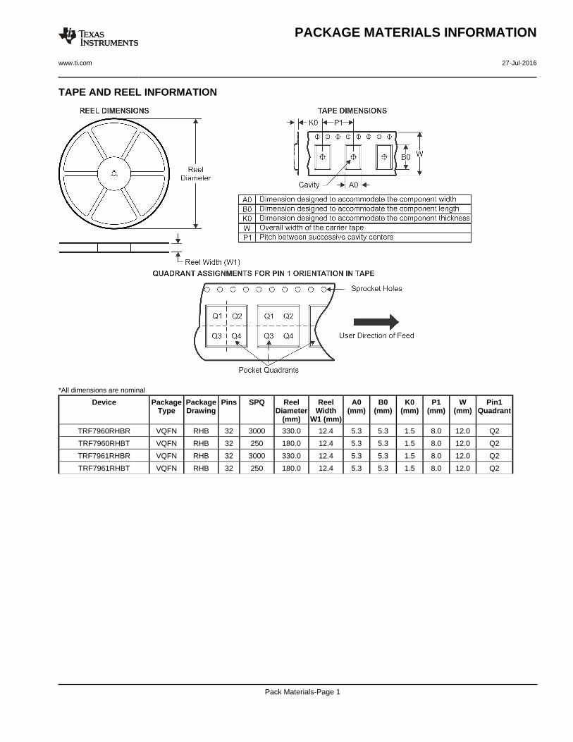
TAPE AND REEL INFORMATION
*All dimensions are nominal
Device PackageType
PackageDrawing
Pins SPQ ReelDiameter
(mm)
ReelWidth
W1 (mm)
A0(mm)
B0(mm)
K0(mm)
P1(mm)
W(mm)
Pin1Quadrant
TRF7960RHBR VQFN RHB 32 3000 330.0 12.4 5.3 5.3 1.5 8.0 12.0 Q2
TRF7960RHBT VQFN RHB 32 250 180.0 12.4 5.3 5.3 1.5 8.0 12.0 Q2
TRF7961RHBR VQFN RHB 32 3000 330.0 12.4 5.3 5.3 1.5 8.0 12.0 Q2
TRF7961RHBT VQFN RHB 32 250 180.0 12.4 5.3 5.3 1.5 8.0 12.0 Q2
PACKAGE MATERIALS INFORMATION
www.ti.com 27-Jul-2016
Pack Materials-Page 1

*All dimensions are nominal
Device Package Type Package Drawing Pins SPQ Length (mm) Width (mm) Height (mm)
TRF7960RHBR VQFN RHB 32 3000 367.0 367.0 35.0
TRF7960RHBT VQFN RHB 32 250 210.0 185.0 35.0
TRF7961RHBR VQFN RHB 32 3000 367.0 367.0 35.0
TRF7961RHBT VQFN RHB 32 250 210.0 185.0 35.0
PACKAGE MATERIALS INFORMATION
www.ti.com 27-Jul-2016
Pack Materials-Page 2


IMPORTANT NOTICE
Texas Instruments Incorporated (TI) reserves the right to make corrections, enhancements, improvements and other changes to itssemiconductor products and services per JESD46, latest issue, and to discontinue any product or service per JESD48, latest issue. Buyersshould obtain the latest relevant information before placing orders and should verify that such information is current and complete.TI’s published terms of sale for semiconductor products (http://www.ti.com/sc/docs/stdterms.htm) apply to the sale of packaged integratedcircuit products that TI has qualified and released to market. Additional terms may apply to the use or sale of other types of TI products andservices.Reproduction of significant portions of TI information in TI data sheets is permissible only if reproduction is without alteration and isaccompanied by all associated warranties, conditions, limitations, and notices. TI is not responsible or liable for such reproduceddocumentation. Information of third parties may be subject to additional restrictions. Resale of TI products or services with statementsdifferent from or beyond the parameters stated by TI for that product or service voids all express and any implied warranties for theassociated TI product or service and is an unfair and deceptive business practice. TI is not responsible or liable for any such statements.Buyers and others who are developing systems that incorporate TI products (collectively, “Designers”) understand and agree that Designersremain responsible for using their independent analysis, evaluation and judgment in designing their applications and that Designers havefull and exclusive responsibility to assure the safety of Designers' applications and compliance of their applications (and of all TI productsused in or for Designers’ applications) with all applicable regulations, laws and other applicable requirements. Designer represents that, withrespect to their applications, Designer has all the necessary expertise to create and implement safeguards that (1) anticipate dangerousconsequences of failures, (2) monitor failures and their consequences, and (3) lessen the likelihood of failures that might cause harm andtake appropriate actions. Designer agrees that prior to using or distributing any applications that include TI products, Designer willthoroughly test such applications and the functionality of such TI products as used in such applications.TI’s provision of technical, application or other design advice, quality characterization, reliability data or other services or information,including, but not limited to, reference designs and materials relating to evaluation modules, (collectively, “TI Resources”) are intended toassist designers who are developing applications that incorporate TI products; by downloading, accessing or using TI Resources in anyway, Designer (individually or, if Designer is acting on behalf of a company, Designer’s company) agrees to use any particular TI Resourcesolely for this purpose and subject to the terms of this Notice.TI’s provision of TI Resources does not expand or otherwise alter TI’s applicable published warranties or warranty disclaimers for TIproducts, and no additional obligations or liabilities arise from TI providing such TI Resources. TI reserves the right to make corrections,enhancements, improvements and other changes to its TI Resources. TI has not conducted any testing other than that specificallydescribed in the published documentation for a particular TI Resource.Designer is authorized to use, copy and modify any individual TI Resource only in connection with the development of applications thatinclude the TI product(s) identified in such TI Resource. NO OTHER LICENSE, EXPRESS OR IMPLIED, BY ESTOPPEL OR OTHERWISETO ANY OTHER TI INTELLECTUAL PROPERTY RIGHT, AND NO LICENSE TO ANY TECHNOLOGY OR INTELLECTUAL PROPERTYRIGHT OF TI OR ANY THIRD PARTY IS GRANTED HEREIN, including but not limited to any patent right, copyright, mask work right, orother intellectual property right relating to any combination, machine, or process in which TI products or services are used. Informationregarding or referencing third-party products or services does not constitute a license to use such products or services, or a warranty orendorsement thereof. Use of TI Resources may require a license from a third party under the patents or other intellectual property of thethird party, or a license from TI under the patents or other intellectual property of TI.TI RESOURCES ARE PROVIDED “AS IS” AND WITH ALL FAULTS. TI DISCLAIMS ALL OTHER WARRANTIES ORREPRESENTATIONS, EXPRESS OR IMPLIED, REGARDING RESOURCES OR USE THEREOF, INCLUDING BUT NOT LIMITED TOACCURACY OR COMPLETENESS, TITLE, ANY EPIDEMIC FAILURE WARRANTY AND ANY IMPLIED WARRANTIES OFMERCHANTABILITY, FITNESS FOR A PARTICULAR PURPOSE, AND NON-INFRINGEMENT OF ANY THIRD PARTY INTELLECTUALPROPERTY RIGHTS. TI SHALL NOT BE LIABLE FOR AND SHALL NOT DEFEND OR INDEMNIFY DESIGNER AGAINST ANY CLAIM,INCLUDING BUT NOT LIMITED TO ANY INFRINGEMENT CLAIM THAT RELATES TO OR IS BASED ON ANY COMBINATION OFPRODUCTS EVEN IF DESCRIBED IN TI RESOURCES OR OTHERWISE. IN NO EVENT SHALL TI BE LIABLE FOR ANY ACTUAL,DIRECT, SPECIAL, COLLATERAL, INDIRECT, PUNITIVE, INCIDENTAL, CONSEQUENTIAL OR EXEMPLARY DAMAGES INCONNECTION WITH OR ARISING OUT OF TI RESOURCES OR USE THEREOF, AND REGARDLESS OF WHETHER TI HAS BEENADVISED OF THE POSSIBILITY OF SUCH DAMAGES.Unless TI has explicitly designated an individual product as meeting the requirements of a particular industry standard (e.g., ISO/TS 16949and ISO 26262), TI is not responsible for any failure to meet such industry standard requirements.Where TI specifically promotes products as facilitating functional safety or as compliant with industry functional safety standards, suchproducts are intended to help enable customers to design and create their own applications that meet applicable functional safety standardsand requirements. Using products in an application does not by itself establish any safety features in the application. Designers mustensure compliance with safety-related requirements and standards applicable to their applications. Designer may not use any TI products inlife-critical medical equipment unless authorized officers of the parties have executed a special contract specifically governing such use.Life-critical medical equipment is medical equipment where failure of such equipment would cause serious bodily injury or death (e.g., lifesupport, pacemakers, defibrillators, heart pumps, neurostimulators, and implantables). Such equipment includes, without limitation, allmedical devices identified by the U.S. Food and Drug Administration as Class III devices and equivalent classifications outside the U.S.TI may expressly designate certain products as completing a particular qualification (e.g., Q100, Military Grade, or Enhanced Product).Designers agree that it has the necessary expertise to select the product with the appropriate qualification designation for their applicationsand that proper product selection is at Designers’ own risk. Designers are solely responsible for compliance with all legal and regulatoryrequirements in connection with such selection.Designer will fully indemnify TI and its representatives against any damages, costs, losses, and/or liabilities arising out of Designer’s non-compliance with the terms and provisions of this Notice.
Mailing Address: Texas Instruments, Post Office Box 655303, Dallas, Texas 75265Copyright © 2017, Texas Instruments Incorporated