transport properties of copper phthalocyanine based organic … · 2018-10-31 · transport...
TRANSCRIPT

Transport properties of copper phthalocyaninebased organic electronic devices
C. Schustera, M. Kraus, A. Opitzb, W. Brutting, and U. Eckern
Institut fur Physik, Universitat Augsburg, 86135 Augsburg, Germany
Abstract. Ambipolar charge carrier transport in Copper phthalocyanine (CuPc)is studied experimentally in field-effect transistors and metal-insulator-semicon-ductor diodes at various temperatures. The electronic structure and the transportproperties of CuPc attached to leads are calculated using density functional theoryand scattering theory at the non-equilibrium Green’s function level. We discuss,in particular, the electronic structure of CuPc molecules attached to gold chainsin different geometries to mimic the different experimental setups. The combinedexperimental and theoretical analysis explains the dependence of the mobilityand the transmission coefficient on the charge carrier type (electrons or holes)and on the contact geometry. We demonstrate the correspondence between ourexperimental results on thick films and our theoretical studies of single moleculecontacts. Preliminary results for fluorinated CuPc are discussed.
1 Introduction
Charge carrier transport in electronic devices is an important topic, experimentally as wellas theoretically. Recently, theoretical progress has been made on different levels, for exam-ple, a parameter-free calculation of the transport behavior has been accomplished for metallicnano-contacts and single-molecule devices [1,2,3]. It also has been possible to determine thetransmission through interfaces, simple metals serving as leads, for example, Fe/MgO/Fe orAu/MgO/Au tunnel junctions [4,5]. In these studies, the ground state properties of the sys-tem within a suitably defined central region, the “scattering region”, are determined with thehelp of density functional theory (DFT) [6]. The electronic energy levels of the individualmolecules, monolayers and crystals in the scattering region largely determine the charge trans-port. Thereby a basic understanding of energy level alignment and the related injection barriersis achieved [7]. Finally, the transmission through the device is obtained by scattering theory atthe non-equilibrium Green’s function level [8].
On the other hand, the temperature-dependent transport properties of organic thin-filmdevices can be modeled as two-dimensional drift-diffusion processes using commercial programs[9]. In the standard device simulation software for hopping transport, the possibility to treat abroad density of states, which would be relevant in the present context, is included. Of course,a combination of the classical stochastic treatment of thin films with the quantum mechanicalDFT approach for single-molecule contacts would be very desirable [10].
As a particular class of planar aromatic compounds, metal phthalocyanines are consideredfor numerous applications since they show a variety of interesting physical and chemical proper-ties. In particular, the semiconducting copper phthalocyanine (CuPc, for the chemical structuresee Fig. 1a) is employed in several optoelectronic devices [11]. It is used as buffer layer in organic
a e-mail: [email protected] e-mail: [email protected]
arX
iv:1
003.
6094
v1 [
cond
-mat
.mes
-hal
l] 3
1 M
ar 2
010
2
light-emitting diodes [12] or as active layer in organic field-effect transistors (OFETs) [13]. Dueto the narrow d-bands of the transition metal and the π-bonding present on the benzene rings,CuPc crystals show effects which can only be accounted for by electronic correlations. The cor-relation effects manifest themselves, for example, in the Mott metal-insulator transition uponK-doping [14,15]. However, in the following we will concentrate on certain aspects of transport,i.e., charge injection and the mobility of charge carriers, since these are of practical interest forapplications in optoelectronic devices.
In this paper we present the results of a combined experimental and theoretical study. Theexperimental results are obtained by measuring field-effect devices, while for the theoreticalpart we employ DFT and the non-equilibrium Green’s function formalism. In both parts thefocus is on the role of the contact geometries. In the following Secs. 2 and 3, we describe theexperimental and the theoretical details, respectively. In Sec. 4 we focus on ambipolar field-effect devices; we find that the experimental characteristics can be well explained on the basisof DFT. Our results for the temperature dependence of the electron and hole mobilities arepresented and discussed in Sec. 5. In Sec. 6 we argue that the mobility experiments can beunderstood by studying a simple model system, namely, a single CuPc molecule, or two CuPcmolecules, attached to Au chains which serve as leads. Finally, we discuss in Sec. 7 some aspectsof fluorinated CuPc, and present a brief summary in Sec. 8.
2 Experimental details
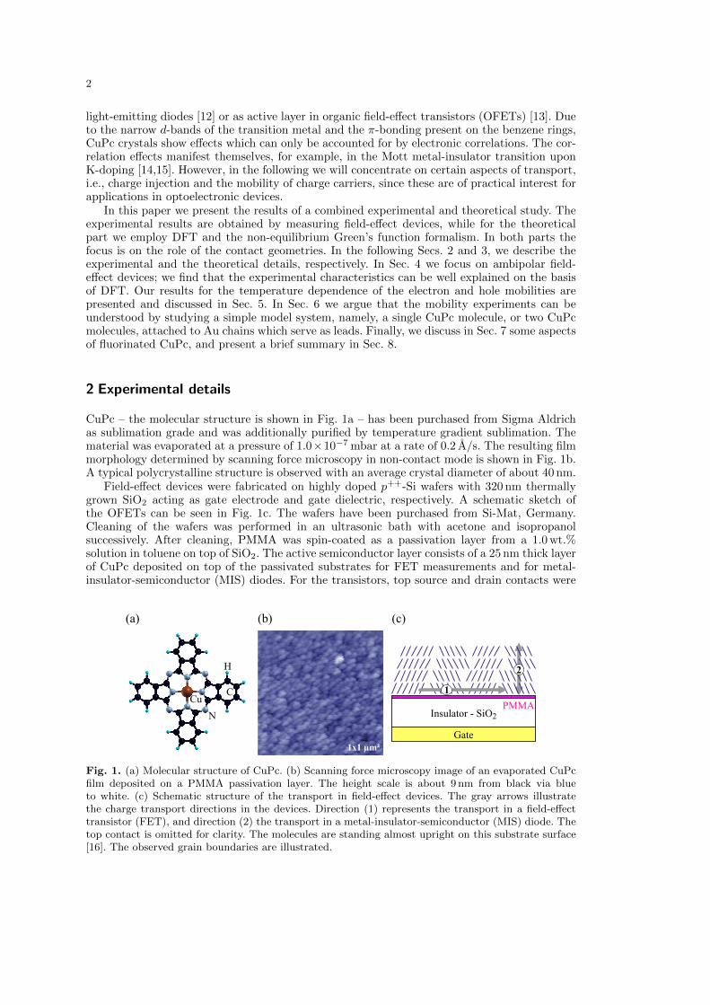
CuPc – the molecular structure is shown in Fig. 1a – has been purchased from Sigma Aldrichas sublimation grade and was additionally purified by temperature gradient sublimation. Thematerial was evaporated at a pressure of 1.0×10⁻⁷ mbar at a rate of 0.2 A/s. The resulting filmmorphology determined by scanning force microscopy in non-contact mode is shown in Fig. 1b.A typical polycrystalline structure is observed with an average crystal diameter of about 40 nm.
Field-effect devices were fabricated on highly doped p++-Si wafers with 320 nm thermallygrown SiO2 acting as gate electrode and gate dielectric, respectively. A schematic sketch ofthe OFETs can be seen in Fig. 1c. The wafers have been purchased from Si-Mat, Germany.Cleaning of the wafers was performed in an ultrasonic bath with acetone and isopropanolsuccessively. After cleaning, PMMA was spin-coated as a passivation layer from a 1.0 wt.%solution in toluene on top of SiO2. The active semiconductor layer consists of a 25 nm thick layerof CuPc deposited on top of the passivated substrates for FET measurements and for metal-insulator-semiconductor (MIS) diodes. For the transistors, top source and drain contacts were
H
C
N
Cu
(a) (b) (c)
1x1 µm²
Insulator - SiO2
Gate
PMMA
2
1
Fig. 1. (a) Molecular structure of CuPc. (b) Scanning force microscopy image of an evaporated CuPcfilm deposited on a PMMA passivation layer. The height scale is about 9 nm from black via blueto white. (c) Schematic structure of the transport in field-effect devices. The gray arrows illustratethe charge transport directions in the devices. Direction (1) represents the transport in a field-effecttransistor (FET), and direction (2) the transport in a metal-insulator-semiconductor (MIS) diode. Thetop contact is omitted for clarity. The molecules are standing almost upright on this substrate surface[16]. The observed grain boundaries are illustrated.

3
evaporated through a shadow mask with various channel lengths in the range of 80µm to 180µmusing different metal contacts with a thickness of 50 nm. In some cases a thin (approximately1 nm) interlayer of the strong organic acceptor F4TCNQ is evaporated between the organicsemiconductor and the metal top contact. The areas of the MIS diodes were about 5.0 mm2,defined by the structure of the semiconductor and the top contact. Transistor characteristicswere measured with a Keithley 4200 semiconductor parameter analyzer, and for the impedancespectroscopy a Solartron 1260 impedance/gain-phase analyzer coupled with a Solartron 1296dielectric interface was used.
In the case of OFETs with different electrode materials the charge carrier mobility wasdetermined using the so-called transmission line method (TLM) [17]. This technique allows toextract the charge carrier mobility µTLM without the disturbing effect of the contact resistance.In most cases the electrode-semiconductor interface is not ideally ohmic but forms a Schottkycontact which causes an injection barrier depending on the relative positions of the HOMOand the LUMO of the semiconductor and the work function of the electrode metal. The totalresistance of the OFET Rtotal is split into the contact resistance RC (which is independent ofthe channel length) and the channel resistance which is proportional to the channel length L.The total resistance is then given by
Rtotal = RC +L
µTLMWCins(VG − VT)(1)
with the channel width W , the specific insulator capacitance Cins, the gate voltage VG and thethreshold voltage VT. Thus, a plot of the total resistance as a function of the channel lengthallows to determine µTLM (slope of the linear fit).
In case of temperature dependent measurements the field-effect mobility is calculated fromthe transfer characteristics in the linear regime, using the following expression for the draincurrent ID
ID =WCins
Lµlin(VG − VT)VD (2)
where VD is the drain voltage. Clearly the mobility µlin can be derived from the slope of thetransfer characteristic, ID versus VG.
In contrast to OFETs where the charge carrier mobility parallel to the semiconductor-insulator interface is measured, in MIS diodes the charge carrier mobility perpendicular tothis interface can be determined. Due to the structural anisotropy of organic semiconductormolecules the overlap of the electronic orbitals and thus the charge carrier transport is com-pletely different in these two directions.
The charge carrier mobility perpendicular to the surface, µMIS, can be determined with thehelp of impedance spectroscopy. The capacitance of the MIS diode is measured as a functionof the applied frequency in the accumulation regime of electrons or holes, i.e., at positiveor negative gate voltage, respectively. For low frequencies, due to the accumulation of chargecarriers at the interface, only the capacitance of the insulating layer Cins (i.e., SiO2 and PMMA)is measured. When the frequency is increased above a characteristic frequency fc the chargecarriers cannot follow the external field any more because of the limited mobility in the CuPclayer. Consequently, at fc the measured capacitance drops to the geometric capacitance of thewhole device, C−1MIS = C−1ins + C−1CuPc. The motion of the charge carriers can be assumed to bedetermined by diffusion [18]. Following this approach, the mobility is given by
µMIS =2πfced
2s
kT(3)
with the elementary charge e, the thickness of the semiconductor ds, the Boltzmann constantk and the temperature T .
3 Computational details
In the following, we analyze the electronic structure, in particular, the charge density of theHOMO (highest occupied molecular orbital) and the LUMO (lowest unoccupied molecular
4
orbital) using density functional theory. In particular, we employ the DFT package SIESTA [19],which relies on a basis set of local atomic orbitals. In addition, SIESTA uses norm-conservingpseudo-potentials in the fully non-local form (Kleinman-Bylander [20]). For the metals Cu andAu, we apply pseudo-potentials including d valence states. Moreover, a double zeta basis setand the generalized gradient approximation (GGA) for the exchange correlation potential areused.
As CuPc contains a transition metal within porphyrin and benzene rings, interaction effectsare expected to be relevant, and we have to choose the “best possible” exchange correlationpotential for the present purpose. In particular, spin polarization is an important ingredient,since Cu2+ shows a significant spin splitting [21]. In a systematic study, Marom et al. calculatedthe electronic structure of CuPc using LDA (local density approximation) and GGA, as well ashybrid functionals like the semi-empirical B3LYP, the non-empirical PBE0, and the screenedSHE03 [22]. They concluded that for CuPc/metal systems the screened hybrid functional isthe best choice, since it performs very well for CuPc and is reasonable also for metals [23].In another study, the B3LYP functional was used to determine and classify molecular orbitals[24]. However, we are predominantly interested in transport properties, i.e., the most importantstates near the Fermi level which are sufficiently well described in GGA [22]; also GGA is thebest choice for noble metals [23]. Hence we rely on the GGA in the following.
Before turning to CuPc molecules in contact with a metal, we summarize the results obtainedfor CuPc monolayers. Monolayers of flat lying molecules are formed on metallic surfaces orgraphite; the typical molecule-molecule distances in a CuPc monolayer on top of a [111] directedsurface of Au [25] or a [110] surface of Ag [26] are larger than the molecule-molecule distances inthe CuPc crystal [27]. The CuPc molecules in a monolayer show different orientations towardseach other, depending on the symmetry of the substrate. However, due to the large molecule-molecule distances within the monolayer the electronic structure of CuPc near the Fermi level isvery similar to that of a single molecule, with only minor effects of the coordination to the othermolecules. We have checked this supposition for an orientation of the molecules to each otherof 60◦ and a molecule-molecule distance of d = 14.4 A (as obtained for a Au[111] substrate),a 90◦ orientation with d = 17.35 A (Ag[110] substrate), and a 45◦ orientation with d = 17.35A. The density of states (DOS) near the Fermi level, shown in Fig. 2, is identical in all theseconfigurations. In addition, it agrees with recent theoretical and experimental results [21,28].We also studied a 45◦ configuration with a smaller distance, d = 13.72 A, corresponding tothe bulk value. In this case, the band gap is slightly smaller, 1.43 eV versus 1.52 eV, than theHOMO-LUMO gap of single molecules, in accordance with previous results [24]. The calculationthus underestimates (as to be expected in LDA and GGA) the experimental gap of 1.8 eV [29].Almost identical photoemission spectra of CuPc thin films [24] and gase phase CuPc [30] alsosuggest that the electronic structure is hardly modified by inter-molecular interactions.
For the discussion of the transport properties we analyze the molecular orbitals near to theFermi level. In particular, the HOMO includes a contribution of a (single occupied) b1g orbitallocalized on the Cu together with the a1u molecular orbital, and the LUMO a b1g orbitaltogether with the eg molecular orbital. The charge density isosurface is obtained by integrating
the DOS, N(E), in a certain energy range, n(r) =∫ E2
E1dEN(E). A plot of the charge density
isosurface of the states contributing to the HOMO (E1 = −1 eV, E2 = −0.65 eV) and theLUMO (E1 = 0.5 eV, E2 = 1 eV) is shown in Fig. 3. Our results for the charge density of theLUMO are very similar to those obtained in [24]. In case of the HOMO, the Cu b1g contributesto the charge density within our calculations (using GGA) but not within the previous studiesusing B3LYP [24]. The most important difference of the HOMO versus the LUMO lies in themissing contribution on the nitrogen in the HOMO. Otherwise the spatial extensions are almostidentical, and hence do not allow conclusions concerning the overlap of the molecules.
4 Ambipolar field-effect devices
Ambipolar charge carrier transport in field-effect devices is related to the accumulation of bothcharge carrier types, electrons and holes, at the semiconductor/insulator interface. To prevent

5
CuPc
E – EF [eV]
DOS[1/eV]
210-1-2
30
25
20
15
10
5
0
Fig. 2. Density of states of CuPc in a spin polarized GGA calculation, for different substrate configu-rations as explained in the main text. A level broadening of 0.1 eV was used for the plot.
Fig. 3. Charge density isosurfaces of relevant orbitals. Top: the HOMO contains contributions fromthe a1u orbital (left hand side) and from the b1g orbital (right hand side) located on copper. Bottom:the LUMO contains contributions from of the eg orbital and from the b1g orbital; here, the sum ofboth contributions is shown.
6
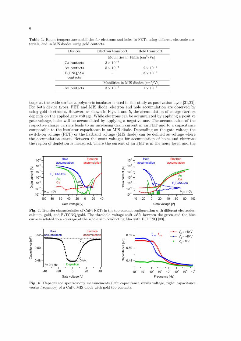
Table 1. Room temperature mobilities for electrons and holes in FETs using different electrode ma-terials, and in MIS diodes using gold contacts.
Devices Electron transport Hole transport
Mobilities in FETs [cm2/Vs]
Ca contacts 3 × 10⁻⁴ –
Au contacts 5 × 10⁻⁴ 2 × 10⁻³
F4CNQ/Aucontacts
– 3 × 10⁻³
Mobilities in MIS diodes [cm2/Vs]
Au contacts 3 × 10⁻⁸ 1 × 10⁻⁸
traps at the oxide surface a polymeric insulator is used in this study as passivation layer [31,32].For both device types, FET and MIS diode, electron and hole accumulation are observed byusing gold electrodes. However, as shown in Figs. 4 and 5, the accumulation of charge carriersdepends on the applied gate voltage. While electrons can be accumulated by applying a positivegate voltage, holes will be accumulated by applying a negative one. The accumulation of therespective charge carriers leads to an increasing drain current in an FET and to a capacitancecomparable to the insulator capacitance in an MIS diode. Depending on the gate voltage theswitch-on voltage (FET) or the flatband voltage (MIS diode) can be defined as voltage wherethe accumulation starts. Between the onset voltages for accumulation of holes and electronsthe region of depletion is measured. There the current of an FET is in the noise level, and the
-100 -80 -60 -40 -20 0 20 40
10-11
10-10
10-9
10-8
10-7
10-6
10-5
∆VT
F4TCNQ/Au
Au
Ca
VD= −10V
Dra
in c
urr
ent [A
]
Gate voltage [V]
Hole
accumulation
Electron
accumulation
-40 -20 0 20 40 60 80 100
10-11
10-10
10-9
10-8
10-7
10-6
10-5
VD= +10V
Dra
in c
urr
ent [A
]
Gate voltage [V]
Hole
accumulation
Electron
accumulation
Au
Ca
F4TCNQ/Au
Fig. 4. Transfer characteristics of CuPc FETs in the top-contact configuration with different electrodes:calcium, gold, and F4TCNQ/gold. The threshold voltage shift ∆VT between the green and the bluecurve is related to a coverage of the whole semiconducting film with F4TCNQ [33].
-40 -20 0 20 40
0.48
0.50
0.52
Cdiode
Cins
f = 0.1 Hz Depletion
Hole
accumulation
Capacitance [nF
]
Gate voltage [V]
Electron
accumulation
10-2
10-1
100
101
102
103
104
105
0.48
0.50
0.52 V
G = +40 V
VG = −40 V
VG = 0 V
Capacitance [nF
]
Frequency [Hz]
fr, ho
fr, el
Fig. 5. Capacitance spectroscopy measurements (left: capacitance versus voltage, right: capacitanceversus frequency) of a CuPc MIS diode with gold top contacts.

7
Fig. 6. Left: Top view of the planar contact. The distances Au-H and Au-C are given by dAu−H/C = 1.37
A. Right: Sideview of the perpendicular contact. The distance Au-Cu is given by dCu−Au = 2.89 A.
capacitance of the MIS diode is defined by a series circuit of the insulator and the semiconductorcapacitance.
The charge carrier type can also be controlled by varying the electrode material (see Fig. 4).By using Ca electrodes instead of Au the injection of electrons is enhanced due to the low workfunction of the electrode material, and unipolar electron transport can be detected. In contrast,by using an F4TCNQ interlayer the injection of electrons can be suppressed and unipolar holetransport is observed. Using TLM, the charge charier mobilities are determined as describedin connection with Eq. (1); see Table 1. For CuPc in the FET configuration the mobility ofholes is almost one order of magnitude higher than the mobility of electrons. The analysis fordifferent electrodes shows that the mobilities are independent of the electrode material [32].
The transition from accumulation to depletion in the MIS diode can be seen in capacitancespectroscopy using capacitance-voltage (C-V ) and capacitance-frequency (C-f) measurements.The mobilities of the ambipolar MIS diode are also given in Table 1. The MIS values are four tofive orders of magnitude lower than the mobilities in the FETs, while the respective differencesof the electron and the hole mobilities are less pronounced.
Our DFT results for a single molecule attached to Au chains show that the electronicstructure near the Fermi level of a contacted molecule is similar to that of an isolated one.Note that in this calculation the contact of the Au chains to the molecule is established via theouter phenyl rings in a planar transport geometry, see Fig. 6, left hand side. (Another contactconfiguration will be discussed in Sec. 6.2.)
Experimentally, this configuration – a prototypical onedimensional system – was realizedby placing the CuPc molecule and the Au atoms with a scanning tunneling microscope (STM)tip on a NiAl substrate [34]. The distances between Au and H, and between Au and C, areobtained by strucutural relaxation; both are equal to d = 1.37 A. The distance between the Auatoms in the chains is fixed to the bulk nearest-neighbor distance of 2.89 A. As Ca does notform chains in nature (and also because the DFT for Ca chains does not converge to a self-consistent solution), we contact the CuPc molecule to bulk Ca in the [001] fcc direction usinga pyramidal contact geometry. Using the planar configuration we can now compare contactsmade of different materials – Au chains versus bulk Ca contacts – to determine the influenceof the material and the dimensionality of the leads. Recently, it was shown in fact that aninsulating six-site Au chain attached to Au chains as compared to pyramidal leads has similartransport properties [35]. In this model study, it was found that due to the different couplingthe molecular levels are shifted by approximatively 0.1 eV in energy, and that most of thedifferences between chain and bulk contacts concern the Au d states in the scattering region.
Concerning the electronic structure of the planar contact, the DOS projected onto the CuPcstates shows contributions at the Fermi level in both cases, i.e., for Au and Ca contacts, seeFig. 7. In addition, the charge density isosurface of the states between −0.3 and 0.7 eV in thecase of Au contacts, and the charge density isosurface of the states between −0.3 and 0.4 eVin the case of Ca contacts, are almost identical, see Fig. 8. For this reason, we expect similartransport properties for Au and Ca contacted molecules. Moreover, the shape of the molecular

8
bulk Ca contactAu chain contact
Cu b1g
projected on CuPc
DOS
E – EF [eV]
DOS[1/eV]
21.510.50-0.5-1-1.5-2
14
12
10
8
6
4
2
0
Fig. 7. DOS for CuPc contacted with Au chains or Ca bulk leads.
Fig. 8. Left: Charge density isosurface at the Fermi level for CuPc contacted with Au chains. Right:same, but CuPc contacted with bulk Ca. In both cases, electrons are injected onto the molecule.
orbital near EF resembles the LUMO of the free molecule, indicating an electron transfer tothe molecule due to the contacts. Analyzing the contributions at the Fermi energy of the Aucontacted molecule in detail, we find that the Cu b1g dominates between −0.3 and 0.3 eV,whereas the eg dominates around 0.5 eV. Thus there is no overlap between the electronic statesof the leads and of the molecule near EF. Since the shape of the molecular orbitals is notinfluenced by the leads, the transport properties can be explained on the basis of the propertiesof an isolated molecule.
It is remarkable that samples with Au electrodes show ambipolar charge carrier transportalthough the work function of Au fits very well to the HOMO of CuPc [32]. This effect canprobably be attributed to the top contacts. However, the work function of the metal and theHOMO level cannot be directly compared because of the formation of interface dipoles at themetal-organic interface that disrupt the vacuum level alignment [36]. Additionally diffusion ofthe metal into the organic film at high deposition temperature [37] and deposition induceddefects at the semiconductor/metal interface [38] have to be considered. Our results indicatethat the effective work function of the top contact Au electrode allows injection of both chargecarrier types, and that it differs from the work function of a bottom contact electrode.

9
Fig. 9. Charge density isosurface at the Fermi level for CuPc contacted with Au chains in a perpen-dicular geometry.
As far as single molecules are concerned, we observe electron injection into the molecule whenthe contact geometry is planar. In order to study hole injection, we thus have to investigateother systems. As a first attempt, we studied another electrode material, namely Pt since ithas the largest work function among the metals used as contacts. However, for this case we findno overlap of the contact states with the molecular states, hence no contributions at the Fermilevel and thus an insulating behavior.
In addition, a different contact geometry was investigated. We use again Au chains asleads but contact the molecule in a perpendicular geometry, see Fig. 6, right hand side. Thuswe contact directly to Cu, simulating a transport measurement along path 1 in Fig. 1c. Thedistance Au-Cu is chosen to be equal to the Au-Au distance within the chains, dCu−Au = 2.89A; for this value, the force between Au and Cu is found to be extremely small. Indeed, injectionof holes, i.e., a charge density isosurface near the Fermi level resembling the HOMO of theisolated molecule, is found in the perpendicular configuration, see Fig. 9. In contrast to Au, Cais expected to have no overlap with the Cu atom of the molecule, therefore the hole injectionfrom Ca into CuPc in a perpendicular geometry should be blocked. Similarly, we have shownrecently for bulk Au that metallic impurites with an electronic structure different from Auoverlap only slightly with the host [39] and thus block the transport.
To summarize briefly, on the basis of DFT for single molecules in contact with a metal wehave shown that electrons are injected in a planar contact, independent of the lead material,whereas holes are injected in the perpendicular configuration with Au as electrode material.The contact resistance and the mobility can be obtained from the transmission coefficient, asdiscussed in Sec. 6.
5 Charge carrier mobility
The temperature dependence of electron and hole mobilities for FETs and MIS diodes is shownin Fig. 10. The hole mobilities determined in an FET are for the whole temperature rangehigher than the electron mobilities, and both are higher than the mobilities determined inan MIS diode. Additionally the temperature dependence of the MIS diode mobilities is morepronounced than the temperature dependence of the FET mobilities. The difference betweenFETs and MIS diodes in terms of charge carrier density and anisotropy will be discussed indetail in the following.

10
Table 2. Activation energies for electrons and holes in ambipolar MIS diodes and ambipolar FETsdetermined by Eq. (4), as well as barrier energies in FETs determined by Eq. (5). In addition, therespective fit parameters, µ0 and vl, are given.
Devices Electron transport Hole transport
Eact [meV] µ0 [cm2/Vs] Eact [meV] µ0 [cm2/Vs]
MIS diode 410 0.41 452 0.45
FET 183 0.18 120 0.19
Ebar [meV] vl [cm2/s] Ebar [meV] vl [cm2/s]
FET 100 56 74 44
First, we present the activation energies Eact in Table 2, as determined by the Arrheniusbehavior of the thermally activated mobility:
µ = µ0 exp
(−Eact
kT
). (4)
Here µ0 is the high temperature limit of the mobility. A strong difference in the activationenergies is observed between the two device types, and also between the two charge carriertypes. While for holes the mobility is higher and the activation energy is lower than for electronsin the FET, the behavior is reversed for the MIS diode. Note also that the activation energiesin the MIS diode are more than two times higher than those in the FET.
While the transport in the FET is restricted to the accumulation layer with a high chargecarrier density, the transport in the MIS diode extends over the whole device thickness. Thusthe charge carrier density in the FET is determined by the effective gate voltage (VG − VT),and is of the order of 1019 cm−3. In contrast the charge carrier density in the MIS diode isdefined by the doping of the material which can be determined from the C-V measurement. Inthe MIS diodes analyzed here the charge carrier density is two orders of magnitude lower thanin an FET.
In order to describe the dependence of the mobility on the charge carrier density extendeddisorder models were introduced. The extended Gaussian disorder model is applicable to poly-meric systems [40,41], while the extended correlated disorder model can be used for molecularmaterials [42]. Both models are reasonable for disordered systems but not for (partially) orderedand anisotropic materials [43]. The scanning force microscopy (SFM) image in Fig. 1b showsthe CuPc film to be polycrystalline; therefore the description using a disorder parameter like
220 240 260 280 300
10-10
10-9
10-8
10-4
10-3
10-2
hole mobility
Mobili
ty [cm
2/V
s]
Temperature [K]
FET
MIS
electron mobility
Fig. 10. Temperature dependent mobilities for FET and MIS diode, and for both charge carrier types.The lines are fits to determine the activation energy using Eq. (4).
11
the width of the Gaussian density of states is not applicable. Instead, for polycrystalline filmsthe activation energy for hopping at the grain boundaries is an important parameter. Hencethe following temperature dependence [44],
µ =evl
8kTexp
(−Ebar
kT
), (5)
was proposed for thermionic emission of charge carriers at grain boundaries, where v is themean charge carrier velocity, and l the grain size. Indeed there is a distinct difference betweenpath 1 and path 2 which is revealed in the SFM image, compare Fig. 1: Grain boundariesare important for the path parallel to the semiconductor/insulator interface (path 1), whichcorresponds to the transport in the FET accumulation layer, while they are obviously absent forthe perpendicular path (path 2). Hence Eq. (5) may be applicable for the FET configuration,and we fit the FET data shown in Fig. 10 also with this formula. The resulting barrier energiesEbar are also given in Table 2. They show the same tendency as the FET activation energies.Note, however, that in view of the limited temperature range of our data both fits, with Eq. (4)and Eq. (5), respectively, are of similar quality. At present the origin of the lower activation orbarrier energy for the hole transport relative to the electron transport remains unclear.
In addition to the difference in charge carrier density and film morphology, the anisotropydue to the ordered arrangement of the molecules needs to be considered. The CuPc moleculesare standing almost upright on the surface as schematically illustrated in Fig. 1c [45]. For thisreason a good π-π overlap is present for the transport parallel to the semiconductor/insulatorinterface. Due to the standing molecules and the formation of π orbitals on the side of thedisc-like molecule, the overlap between CuPc molecules standing on top of each other is lesspronounced. However, no models are available at present which are able to describe the chargecarrier density dependence, the anisotropic behavior of the transport, and the transport overgrain boundaries in organic films consistently.
6 Transmission through a Au/CuPc/Au model system
In this section, we present our results for simple model systems, namely a single CuPc molecule,as well as two CuPc molecules, which are contacted by two gold chains, respectively. As men-tioned above, we are able to explain the main features of the experimental results on the basisof these models.
6.1 Contact resistance
We first study a single CuPc molecule to which Au chains are attached. In addition to theelectronic structure, we determine the transmission coefficient and hence the conductance, fromwhich we are able to draw conclusions about the contact resistance at the metal-moleculeinterface.
Several methods based on electronic structure calculations have been developed to addressthe problem of transmission through nano-contacts. In particular, two-terminal contact mea-surements are treated. (Note that, in contrast to the experimental situation, we do not applya gate voltage in our studies.) Most computational methods rely on a combination of DFTand a scattering theory at the non-equilibrium Green’s functions level, based on the Landauer-Buttiker scheme. The metallic leads are connected to a central region, in which the scatteringtakes place. In particular, we employ the TRANSIESTA [2] and the SMEAGOL program pack-age [3]. Both packages rely on the SIESTA code but treat the surface Green’s function differ-ently. Within SMEAGOL, the I-V curve is calculated self-consistently with a voltage dependenttransmission coeffcient.
In the Landauer-Buttiker formalism, the self-energies of the left (L) and right (R) leadare calculated first. As metallic leads are used, the screening within the leads ensures thatthe distortion due to the contact-interface region decays within a few nanometers. Then the
12
leads are connected to a central region of interest (molecule, nano-contact, interface). Thus aneffective description of the central region (C) emerges which includes the properties of the leads(L,R). In equilibrium, the transmission coefficient is given by the retarded Green’s function GC
of the central region and the lead self energies ΣL/R. With ΓL/R = i[ΣL/R(E)−Σ†L/R(E)], one
finds [8]
T (E, V = 0) = Tr[ΓLG†CΓRGC ] . (6)
Then, the conductance is given by [46] G = 2e2
h T (EF ), where the factor of two accounts for thespin. Here and below we are using a short-hand notation, omitting, in particular, the spatialvariables. For details, see, e.g., Ref. [3].
Applying an external transport voltage V , non-equilibrium Green’s functions have to beconsidered, for example, the lesser Green’s function
G<C(E) = iGC(E)[ΓL(E − eV/2)f(E + eV/2)
+ΓR(E + eV/2)f(E − eV/2)]G†C(E) , (7)
from which the charge density can be obtained. The Fermi function is denoted by f . Further-more, the charge current is given by [8]
I(V ) =2e
h
∫dE T (E, V )[f(E + eV/2)− f(E − eV/2)] , (8)
where T (E, V ) is the voltage-dependent generalization of Eq. (6).Having discussed above the electronic structure of CuPc attached to Au chains in great
detail, we turn now to the transport properties. Concerning the planar contact geometry, thetransmission coefficient does not show a resonance at the Fermi level, in contrast to the DOSprojected on the CuPc states, see Figs. 11a and 11b. To allow for an easy comparison of DOSand T (E), we scaled the DOS by 0.04 (and omitted the units). As the molecular b1g state atthe Fermi level has no spatial overlap with the leads, it does not contribute to the transmission.At the resonant molecular energy levels, given by the a1u and eg molecular orbitals at −1.1eV and 0.3 eV, the transmission coefficient tends to one. At the Fermi energy it is given byTpar(EF ) = 0.94 · 10−3.
The off-resonance transmission coefficient of the perpendicular contact geometry clearly islarger than in the planar configuration, see Fig. 11b. The states related to the molecular a1uorbital are found predominantly at −0.2 eV in the DOS, but they extend to the Fermi level.The bonding and anti-bonding b1g states which have a spatial overlap with the Au chains arelocated at±0.6 eV. Thus we find an energy difference of 1.2 eV between the transmitting orbitalsalong the Au-Cu-Au path. However, in the perpendicular geometry the molecular orbital nearEF also opens a transport channel via an Au-N-Au path. Due to this additional channel, theconductance is more than one order of magnitude larger for the perpendicular contact thanfor the planar case. The perpendicular transmission coefficient at the Fermi energy is given byTperp(EF ) = 0.037 ≈ 39Tpar(EF ).
The I-V characteristics for the planar and the perpendicular contact are shown in Fig. 11c.For the planar contact, we find an approximately linear I-V characteristic at low voltage. Withincreasing voltage, the transmission becomes resonant and the I-V dependence non-linear,I ∝ V 3/2. The I-V characteristic of the perpendicular contact can be described by I ∝ V 1.28,up to a voltage of ≈ 1 V. Hence, the current through the perpendicular contact is predicted tobe about one to two orders of magnitude larger than in the planar one.
6.2 Intermolecular transport
As the transport in the diodes does not only depend on the injection at the contact, i.e., on thecontact-molecule coupling, but also on the transport from molecule to molecule, we study thisquestion by considering two molecules within the central region. However, in order to be able

13
T(E)DOS
planar contact
x0.04
E – EF [eV]
1.510.50-0.5-1-1.5
1
0.8
0.6
0.4
0.2
0
(a)
T(E)DOS
perp. contact
x0.04
E – EF [eV]
10.50-0.5-1
1
0.8
0.6
0.4
0.2
0
(b)
plan. contactperp. contact
voltage [V]
current[µA]
10.80.60.40.20
10
1
0.1
0.01
0.001
(c)
Fig. 11. (a) DOS projected on the CuPc states and T (E) ≡ T (E, 0) of a single CuPc molecule in theplanar contact geometry. (b) same, in the perpendicular contact geometry. (c) I-V characteristics ofboth contacts.
to simulate a crystal-like arrangement, we will also place the last Au atoms of the chains nearthe N atoms between the benzene rings, as indicated in Fig. 12, left hand side, even though inSTM experiments this case is found to be less stable than the contact to H-C-H [34]. Then themolecules rotate by 45◦, similar to the crystal [21]; we call this arrangement π/4 configuration.In the perpendicular geometry we arrange the molecules as shown in Fig. 12, right hand side.
We first compare the electronic structure of the molecular states of the standard and theπ/4 planar contact for the single-molecule case (with Au chains attached). In fact there areonly minor differences, see Fig. 13, left panel. The molecular a1u orbital is shifted upwards to−0.9 eV in the π/4 planar contact. The contribution of the eg orbital extends from 0.3 eVto 0.6 eV in both the standard and the π/4 contact. The main difference concerns the Cu b1g
orbital which is shifted below the Fermi level, to −0.4 eV, leading to a nearly insulating contact.Thus the conductance is considerably smaller for the π/4 than for the standard planar contact,even though the transmission through the π/4 planar contact shows a resonant level at the b1g
energy, because a spatial overlap of Au and Cu is possible in this geometry; compare Fig. 14,left hand side. In all cases, the CuPc DOS of one versus two molecules in the contact region isvery similar, which is demonstrated for the perpendicular contact in Fig. 13, right panel.

14
Fig. 12. Left: View from above onto the planar contact with two molecules in the scattering region.Right: Sideview of the perpendicular contact. The Cu-Cu distances d = 13.72 A (planar) and d = 3.79A (perpendicular), respectively, are chosen similar to the distances within a CuPc crystal.
π/4 planarplanar
b1g
ega1u
CuPc-DOS
planar geometry
E – EF [eV]
DOS[1/eV]
10.50-0.5-1
25
20
15
10
5
0
2 CuPc1 CuPc
b1gb1g
a1u
CuPc-DOS
perpendicular geometry
E – EF [eV]
DOS[1/eV]
10.50-0.5-1
25
20
15
10
5
0
Fig. 13. DOS projected on CuPc. Left: Comparison of the standard and the π/4 planar configuration,for a single molecule attached to Au chains. Right: Comparison of contacts with one and two molecules,for the perpendicular configuration.
2 CuPc1 CuPc
E – EF [eV]
T(E
)
10.50-0.5-1
10−1
10−2
10−3
10−4
10−5
10−6
10−7
10−8
10−9
2 CuPc, perp.1 CuPc, perp.
voltage [V]
current[µA]
10.80.60.40.20
10
1
0.1
0.01
0.001
Fig. 14. Left: Logarithmic plot of T (E) in the π/4 planar configuration. Right: Current through oneor two molecules in the perpendicular configuration.

15
F16CuPcCuPc
E – EF (eV)
DOS[1/eV]
21.510.50-0.5-1-1.5-2
18
16
14
12
10
8
6
4
2
0
F16CuPc contacted to Au
E – EF (eV)
DOS[1/eV]
21.510.50-0.5-1-1.5-2
18
16
14
12
10
8
6
4
2
0
Fig. 15. Left: DOS of F16CuPc compared to the DOS of CuPc. Right: DOS projected on F16CuPc,when contacted to Au chains in the planar configuration.
However, the conductance of the planar contact (standard and π/4) is reduced by a factorof 10−5 when two molecules are placed within the contact as compared to a single molecule;the corresponding ratio for a perpendicular contact is only 10−2, compare Fig. 14. Hence forboth contact types, the transport will be determined by the small molecule-molecule coupling,and we can expect that the ratio 10−5/10−2 = 10−3 also determines the ratio of mobilities: thisassertion roughly agrees with the data, see Table 1.
We suggest that the three to five orders of magnitude difference between the mobilities canalso be understood classically by considering the lattice structure. (See also the discussion pre-sented in the previous section, last paragraph.) The mobility in the planar contact configurationessentially is determined by hopping processes along the molecules, the distance being about14 A, while the hopping perpendicular to the molecular plane has to overcome a distance of 3A only. Thus the large factor of three orders of magnitude obtained above indeed appears tobe reasonable.
7 Predictions for fluorinated CuPc
Fluorinated F16CuPc, where all H atoms are replaced by F atoms, shows a different behavior.In particular, the Cu b1g state is shifted to lower energy as compared to CuPc, and the bandgap is reduced; see Fig. 15, left hand side. Our measurements still have to be analyzed in detail,but F16CuPc appears to show electron transport only [47].
Within a planar contact geometry, the DOS projected on F16CuPc, see Fig. 15, right handside, shows a peak structure different from the isolated molecule and different from CuPcin the same geometry. Concerning the charge density isosurface corresponding to the statescontributing to the symmetric peak at EF, it is not spread over the whole molecule as in thecase of CuPc but quenched towards the transport axis, see Fig. 16. The shape of the chargedensity does not resemble the charge density of an isolated molecule (in strong contrast toCuPc).
The transmission through F16CuPc in the planar contact is expected to be higher thanthrough CuPc since the DOS shows states at the Fermi level, and the corresponding chargedensity reveals a strong overlap between the leads and the molecular states. Considering theDFT results for F16CuPc in the perpendicular contact, we see that the a1u orbital is shiftedfurther downwards below the Fermi level. Thus hole transmission through F16CuPc should besignificantly smaller than through CuPc in the perpendicular configuration. This agrees withexperiment as mentioned above. On the other hand, electron transport through F16CuPc isenhanced compared to CuPc in the perpendicular configuration.

16
Fig. 16. Charge density isosurface of the states at EF for F16CuPc contacted with Au chains.
8 Summary
In summary, our experiments have demonstrated ambipolar transport in CuPc films, i.e., elec-trons and holes move at the same time. We have identified the two relevant transport paths,path 1 (field-effect transistor (FET), simulated by the perpendicular contact geometry) andpath 2 (metal-insulator-semiconductor (MIS) diode, simulated by the planar contact geome-try), compare Fig. 1. The mobility is by roughly five orders of magnitude larger for the FETthan for the MIS diode geometry. For the FET, the hole mobility is larger than the electronmobility, while for the MIS diode this behavior is reversed. We have analyzed the temperaturedependence of the mobilities using Eqs. (4) and (5), thereby defining the activation and thebarrier energy, respectively. For the FET, the activation and the barrier energy for holes aresmaller than for electrons, while for the MIS diode the activation energy for electrons is thesmaller quantity. However, the temperature range of our experimental data does not allow dis-criminating between the minor difference in the temperature dependence presented by Eqs. (4)and (5).
Since the transport properties of CuPc are hardly affected by the electrode material, webased our theoretical modeling on the assumption that only intrinsic properties are of relevance.As model systems, we studied molecular nano-contacts, i.e., one or two CuPc molecules attachedto metallic leads. The MIS diode geometry was simulated in a planar contact configuration,where CuPc molecules have been placed between Au chains. The FET geometry was mimicedsimilarly in a perpendicular configuration. The theoretical modeling of the geometry realized inthe FET measurments reveals that the preferred charge carriers are indeed holes, in agreementwith the experiments, because the HOMO of the molecule is shifted upwards towards the Fermilevel due to the coupling with the Au chains. In contrast, for the parallel contact geometry(MIS diode) the coupling to the chains shifts the LUMO level downwards and consequently thefavored charge carriers are electrons. Accordingly, in the MIS diode electrons are found to havea higher mobility than holes. From these results, the coupling of the electrodes to the molecularorbitals apparently is the reason for the asymmetry between the charge carrier types.
To gain a better understanding of the inter-molecular transport we also considered contactswith two molecules in the central region. We find that in both cases, planar and perpendicular,the transport is dominated by the molecule-molecule coupling. In particular, we find that thiscoupling is much smaller for the planar (MIS diode) than for the perpendicular (FET) contact,in agreement with the experimental results. We have presented arguments which indicate thatthis observation may be related, from a classical point of view, to the anisotropic structure ofthe molecules, which leads to very different hopping path lengths in the MIS diode versus theFET.
Of course, further theoretical studies are needed since it is not straightforward to relatethe results of quantum-mechanical transport calculations to room-temperature measurements.

17
However, in the latter case, it is also very important to identify the relevant energy levels andtheir wavefunctions, as well as their overlap, in order to gain a microscopic understanding ofthe hopping processes which are responsible for high-temperature transport.
Finally we have presented preliminary results for transport through F16CuPc. In this con-text, further experimental and theoretical investigations are clearly needed.
C.S. and U.E. acknowledge helpful discussions with U. Schwingenschlogl and I. Mertig. The Aupseudopotential was provided by X. Lopez (ETSF, Palaiseau, France). The Smeagol project (SS) issponsored by the Science Foundation of Ireland. This work was supported by the German ResearchFoundation (DFG) through SFB 484 and TRR 80, and by the German Academic Exchange Service(DAAD).
References
1. P. Damle, A.W. Ghosh, S. Datta, Chem. Phys. 281, 171 (2002)2. M. Brandbyge, J.-L. Mozos, P. Ordejon, J. Taylor, K. Stokbro, Phys. Rev. B 65, 165401 (2002)3. A.R. Rocha, V.M. Garcia-Suarez, S.W. Bailey, C.J. Lambert, J. Ferrer, S. Sanvito, Nature Mater.
4, 335 (2005); Phys. Rev. B 73, 085414 (2006)4. I. Rungger, O. Mryasov, S. Sanvito, Phys. Rev. B 79, 094414 (2009)5. M.M. Fadlallah, C. Schuster, U. Schwingenschlogl, I. Rungger, U. Eckern, Phys. Rev. B 80, 235332
(2009)6. W. Kohn, L.J. Sham, Phys. Rev. 140, A1133 (1965)7. J.-L. Bredas, D. Beljonne, V. Coropceanu, J. Cornil, Chem. Rev. 104, 4971 (2004)8. Y. Meir, N. S. Wingreen, Phys. Rev. Lett. 68, 2512 (1992)9. G. Paasch, S. Scheinert, Syn. Metals 122, 145 (2001)
10. P. Lugli, C. Erlen, A. Pecchia, F. Brunetti, L. Latessa, A. Bolognesi, G. Csaba, G. Scarpa, A. diCarlo, Appl. Phys. A 87, 593 (2007)
11. Y. Shirota, H. Kageyama, Chem. Rev. 107, 953 (2007)12. S.M. Tadayyon, H.M. Grandin, K. Griffiths, P.R. Norton, H. Aziz, Z.D. Popovic, Org. Electron. 5,
157 (2004)13. M. Minagawa, K. Shinbo, K. Usuda, T. Takahashi, M. Iwasaki, K. Kato, F. Kaneko, Jpn. J. Appl.
Phys. 45, 8890 (2006)14. M.F. Craciun, S. Rogge, A.F. Morpurgo, J. Am. Chem. Soc. 127, 12210 (2005); M.F. Craciun, S.
Rogge, M.J.L. den Boer, S. Margadonna, K. Prassides, Y. Iwasa, A.F. Morpurgo, Adv. Mater. 18,320 (2006)
15. G. Giovannetti, G. Brocks, J. van den Brink, Phys. Rev. B. 77, 035133 (2008)16. A. Hoshino, Y. Takenaka, H. Miyaji, Acta Crystallogr. B 59, 393 (2003)17. S. Luan, G.W. Neudeck, J. Appl. Phys. 72, 766 (1992)18. P. Stallinga, A.R.V. Benvenho, E.C.P. Smits, S.G.J. Mathijssen, M. Colle, H.L. Gomes, D.M. de
Leeuw, Org. Electron. 9, 735 (2008)19. J.M. Soler, E. Artacho, J.D. Gale, A. Garcıa, J. Junquera, P. Ordejon, D. Sanchez-Portal, J. Phys.:
Condens. Matter 14, 2745 (2002)20. L. Kleinman, D.M. Bylander, Phys. Rev. Lett. 48, 1425 (1982)21. B. Bialek, I.G. Kim, J.I. Lee, Thin Solid Films 436, 107 (2003)22. N. Marom, O. Hod, G.E. Scuseria, L. Kronik, J. Chem. Phys. 128, 164107 (2008)23. J. Paier, M. Marsman, G. Kresse, J. Chem. Phys. 127, 024103 (2007)24. V.Yu. Aristov, O.V. Molodtsova, V.V. Maslyuk, D.V. Vyalikh, V.M. Zhilin, Yu.A. Ossipyan, T.
Bredow, I. Mertig, M. Knupfer, Appl. Surf. Sci. 254, 20 (2007); O.V. Molodtsova, M. Knupfer,V.V. Maslyuk, D.V. Vyalikh, V.M. Zhilin, Y.A. Ossipyan, T. Bredow, I. Mertig, V.Yu. Aristov, J.Chem. Phys. 129, 154705 (2008); V.Yu. Aristov, O.V. Molodtsova, V.V. Maslyuk, D.V. Vyalikh,V.M. Zhilin, Yu.A. Ossipyan, T. Bredow, I. Mertig, M. Knupfer, J. Chem. Phys. 128, 34703 (2008)
25. T. Fritz, M. Hara, W. Knoll, H. Sasabe, Mol. Cryst. Liq. Cryst. 253, 269 (1994)26. F. Song, H. Huang, W. Dou. H. Zhang, Y. Hu, H. Qian, H. Li, P. He, S. Bao, Q. Chen, W. Zhou,
J. Phys.: Condens. Matter 19, 136002 (2007)27. C.J. Brown, J. Chem. Soc. (A), 2488 (1968)28. S.F. Alvarado, L. Rossi, P. Muller, W. Rieß, Synthetic Metals 122, 73 (2001)29. S. Krause, M.B. Casu, A. Scholl, E. Umbach, N. J. Phys. 10, 085001 (2008)

18
30. J. Berkovitz, J. Chem. Phys. 70, 2819 (1979)31. L.L. Chua, J. Zaumseil, J.F. Chang, E.C.W. Ou, P.K.H. Ho, H. Sirringhaus, R.H. Friend, Nature
434, 194 (2005)32. A. Opitz, M. Kraus, M. Bronner, J. Wagner, W. Brutting, New J. Phys. 10, 065006 (2008)33. Y. Abe, T. Hasegawa, Y. Takahashi, T. Yamada, Y. Tokura, Appl. Phys. Lett. 87, 153506 (2005)34. G.V. Nazin, Qiu, W. Ho, Science 302, 77 (2003)35. T. Wunderlich, DFT calculations for the transport through metallic nanocontacts [in German],
diploma thesis, Augsburg, July 2009 (unpublished)36. L. Yan, N.J. Watkins, S. Zorba, Y. Gao, and C. W. Tang, Appl. Phys. Lett. 79, 4148 (2001)37. M. Scharnberg, J. Hu, J. Kanzow, K. Ratzke, R. Adelung, F. Faupel, C. Pannemann, U. Hillering-
mann, S. Meyer, J. Pflaum, Appl. Phys. Lett. 86, 024104 (2005)38. G. Parthasarathy, P.E. Burrows, V. Khalfin, V.G. Kozlov, S.R. Forrest, Appl. Phys. Lett. 72, 2138
(1998)39. M.M. Fadlallah, C. Schuster, U. Eckern, U. Schwingenschlogl, EPL 89, 47003 (2010)40. R. Coehoorn, W.F. Pasveer, P.A. Bobbert, M.A.J. Michels, Phys. Rev. B 72, 155206 (2005)41. W.F. Pasveer, J. Cottaar, C. Tanase, R. Coehoorn, P.A. Bobbert, P.W.M. Blom, D.M. de Leeuw,
M.A.J. Michels, Phys. Rev. Lett. 94, 206601 (2005)42. M. Bouhassoune, S.L.M. van Mensfoort, P.A. Bobbert, R. Coehoorn, Org. Electron. 10, 437 (2009)43. S. Grecu, M. Roggenbuck, A. Opitz, W. Brutting, Org. Electron. 7, 276 (2006)44. R. Bourguiga, M. Mahdouani, S. Mansouri, G. Horowitz, Eur. Phys. J. Appl. Phys. 39, 7 (2007)45. K. Xiao, Y. Liu, G. Yu, D. Zhu, Appl. Phys. A 77, 367 (2003)46. M. Buttiker, Y. Imry, R. Landauer, S. Pinhas, Phys. Rev. B 31, 6207 (1985)47. Z. Bao, A.J. Lovinger, J. Brown, J. Am. Chem. Soc. 120, 207 (1998)