transparent antennas: out of sight, out of mind
TRANSCRIPT

Transparent Antennas: Out of Sight, Out of Mind How a new transparent antenna material delivers peace of mind solving wireless design challenges of 5G, IoT and automotive safety systems
www.chasmtek.com
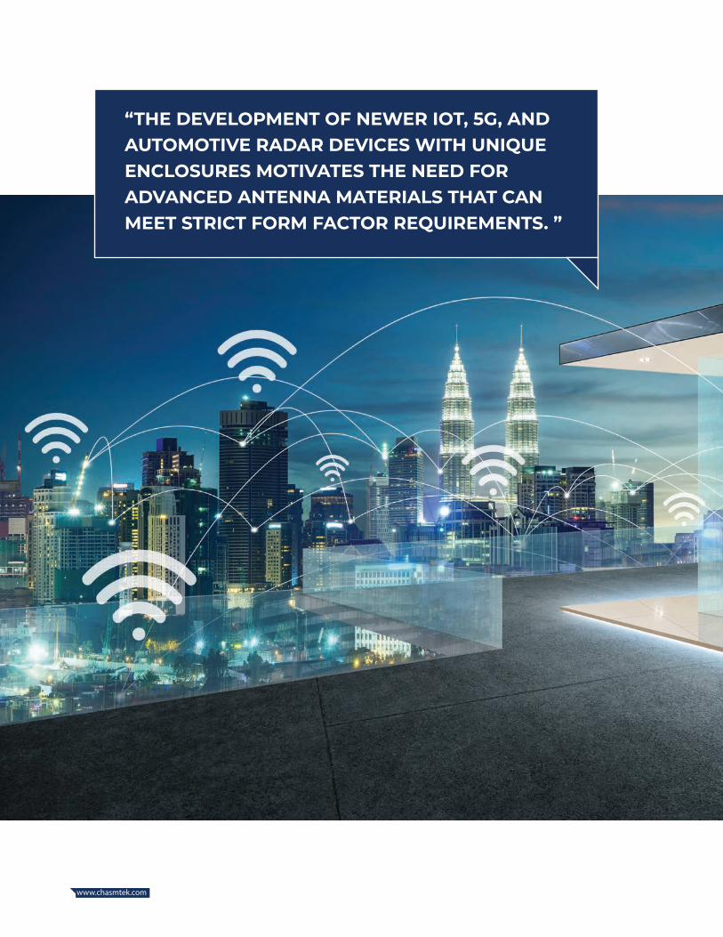
“THE DEVELOPMENT OF NEWER IOT, 5G, AND AUTOMOTIVE RADAR DEVICES WITH UNIQUE ENCLOSURES MOTIVATES THE NEED FOR ADVANCED ANTENNA MATERIALS THAT CAN MEET STRICT FORM FACTOR REQUIREMENTS. ”
www.chasmtek.com
ith origins reaching back to
ALOHAnet in 1971, a
confluence of protocol
advancements and mass adoption of devices
such as smartphones have cemented “cutting
the cord” using RF signals as the preferred
method of connectivity for an ever-growing
array of data consuming devices. Despite the
rapid escalation in wireless speed and the
explosion in connected devices, the technology
enabling all this connectivity – the antenna –
has failed to keep pace with these technological
advancements.
With the rollout of 5G necessitating more
antennas closer to the point of use to achieve
high-bandwidth line of sight connections
and manufacturers seeking to retrofit IoT
connectivity in a broad range of devices,
have performance and design requirements
finally exceeded the capabilities provided by
existing antenna materials? If antennas could
be made transparent, escaping the bounds of
an enclosure, could they “hide in plain sight” or
be adhered to the outside of existing devices to
overcome the challenges of new applications?
Better yet, could this new material deliver equal
or better performance to traditional materials
so not requiring the rationalization of design
tradeoffs typically found with new materials?
A new class of transparent conductive material
– CNT hybrids – delivers the conductivity
required for high performance antenna
applications while achieving near transparency
to effectively make antennas disappear.
Currently being used to revolutionize IoT
products, 5G antenna arrays, and automotive
sensors, this white paper presents a range of
commercially available alternative materials and
how the CNT hybrid empowers designers with
new options for innovation.
INTRODUCTION
W

www.chasmtek.com
NEXT-GEN MATERIALS BRING NEXT-GEN ANTENNAS
It is often said that necessity is the mother
of invention, but the history of science and
technology has shown that the reverse is often
true. As the telecom industry has grown and
matured, and as higher over-the-air data rates have
become available, computing workloads can be
moved from the cloud to the edge, which opens
up applications that were formerly the stuff of
science fiction. Future IoT devices and 5G products
will be processing more data at the edge than ever
before, and all while communicating with each
other and the cloud. Newer automobiles will also
need to communicate with each other and smart
infrastructure over VANETs, and they will make
greater use of short and long-range radar for ADAS
systems, all operating at high GHz frequencies.
The key factor enabling these systems and
applications is highly efficient antennas with
small form factors and low loss tangent at 10-100
GHz frequencies. When we look at desired form
factors for 5G, IoT, and automotive systems, a
flexible, transparent antenna material enables new
applications that are difficult or impossible with
current materials. experience.
www.chasmtek.com
The current antenna solution for these
products is copper phased array antennas,
which must be etched onto a PCB laminate
with low loss tangent at such high frequencies.
Other small form factor solutions on the
market include chip antennas, a variety of
SoCs, and transceiver modules with integrated
antennas operating in WiFi, Bluetooth, cellular,
and K or W radar bands. These solutions
respectively provide antennas with very low
sheet resistance or high efficiency in specific
RF bands. However, the specialized PCB
laminates required to support these solutions
carry high costs and restrict designers to
planar antennas behind an enclosure. As a
result, the enclosure can still interfere with
antenna transmission/reception.
TCFs are one class of materials that provide
a solution to these design challenges in the
above areas. Any TCF must provide high
efficiency, high gain, low cost, and low profile,
as well as being easily fabricated with unique
geometry. A flexible TCF with low sheet
resistance can be easily molded to a device
enclosure and function as a highly efficient
transparent antenna. By engineering the
supporting substrate, it becomes possible
to tune absorption to the desired RF band
without sacrificing transparency at visible
wavelengths. Using a transparent frequency-
selective surface (FSS) material as a ground
plane also allows the directionality of the
antenna in various frequency bands to be
tuned. This ability to adapt the material to
unique enclosures, tune the absorption band,
and tune the radiation pattern with an FSS
helps designers maximize signal strength and
provide desired directionality. Cost is also a
critical factor to ensure scalability and to satisfy
upcoming market demand for TCFs, which is
expected to exceed $5 billion by 2022.
Image: Courtesy CHASM - TCF Antenna AgeNT-1www.chasmtek.com

www.chasmtek.com
THE CURRENT STATE OF TCFS AS POSSIBLE ANTENNA MATERIALS
Although not particularly new, the variety of
flexible TCFs reported in the literature and on
the market is extensive, and many materials
have been specialized for different products.
The current range of flexible TCFs includes
metal oxides, conductive polymers, metal
nanostructures, and MMs.
While these materials can be fabricated on
a flexible substrate like PET, they all carry
some common disadvantages that inhibit
scalable manufacturing or their use as high
efficiency antenna materials in high-GHz RF
products. The primary design requirements
for commercializable flexible TCFs as antenna
materials are:
• Low sheet resistance: Designers that want
flexible TCFs for antennas need a material
with sheet resistance not greater than 1
OPS.
• High VLT and low haze: Transparent
conductors should be nearly invisible (at
least 90% VLT) and have less than 5% haze.
• Simple manufacturing process: The
fabrication process for an ideal flexible TCF
should be easy to scale and carry low costs.
The number of deposition, curing, etching,
and cleaning steps should be minimized.
• Patterning over a large area: A larger
has a larger absorption cross section for
detecting low-level signals. A flexible TCF
antenna should be scalable up to any
desired size with patterned geometry.
Metal nanostructures
Metal nanostructures satisfy the first design
requirement listed above, but they have
significant haze and are translucent with
low VLT in the visible range. They are also
costly to manufacture on transparent flexible
substrates at the scale needed for their
envisioned applications, requiring processes
like photolithography for substrate patterning,
followed by sputtering, solution growth, or
vapor deposition.
www.chasmtek.com

“ANY TCF MUST PROVIDE HIGH EFFICIENCY, HIGH GAIN, LOW COST, AND LOW PROFILE, AS WELL AS BEING EASILY FABRICATED WITH UNIQUE GEOMETRY. ”
www.chasmtek.com
MM Films
MMs are similarly un-promising as
GHz antenna materials thanks to their
sheet resistance of at least ~3 OPS.
These materials can be nearly invisible
as long as the mesh size is less than ~6
microns, but fabricating this pattern
requires an electroless copper process or
photolithography process, both of which
are followed by etching.
Patterned Transparent Metal Oxide Films
Other materials, such as metal oxide TCFs,
only satisfy the fourth design requirement.
Getting sheet resistance below 2.5 OPS
is a major challenge, making these
materials unsuitable for use as high-
efficiency antennas. The morphology
of these materials makes them hazy
with insufficient VLT (up to ~80%) for
antenna applications. The patterning
process for metal oxide TCFs is inefficient
in that it requires a subtractive process,
or it requires direct pattern deposition
with a photolithographic process. Using
photolithography allows the desired
conductor pattern to be deposited directly
on the substrate, but it requires multiple
develop, etch, strip, and cleaning steps,
just as is the case with MMs. Laser ablation
is also useful for patterning on glass, but it
can damage a flexible plastic or polymer
substrate. This process also requires
significant laser time, which increases
overall patterning costs.
Conductive Polymers
Conductive polymers run the gamut
on satisfying these requirements. Ag
nanowires mixed with PEDOT:PSS
(a popular TCF) provides very high
transparency, but its sheet resistance is
much too large for use as an antenna. It
remains to be seen whether a conductive
polymer TCF material with high VLT can be
found and produced at scale.
www.chasmtek.com
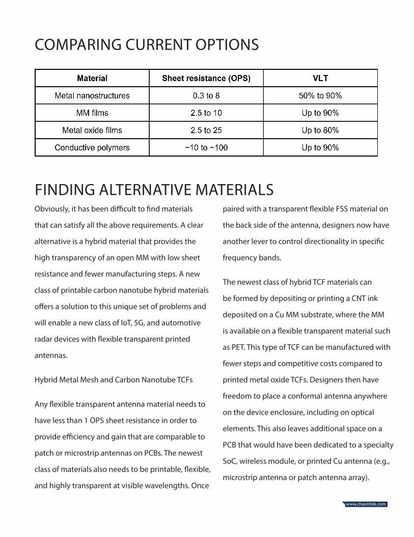
COMPARING CURRENT OPTIONS
FINDING ALTERNATIVE MATERIALSObviously, it has been difficult to find materials
that can satisfy all the above requirements. A clear
alternative is a hybrid material that provides the
high transparency of an open MM with low sheet
resistance and fewer manufacturing steps. A new
class of printable carbon nanotube hybrid materials
offers a solution to this unique set of problems and
will enable a new class of IoT, 5G, and automotive
radar devices with flexible transparent printed
antennas.
Hybrid Metal Mesh and Carbon Nanotube TCFs
Any flexible transparent antenna material needs to
have less than 1 OPS sheet resistance in order to
provide efficiency and gain that are comparable to
patch or microstrip antennas on PCBs. The newest
class of materials also needs to be printable, flexible,
and highly transparent at visible wavelengths. Once
paired with a transparent flexible FSS material on
the back side of the antenna, designers now have
another lever to control directionality in specific
frequency bands.
The newest class of hybrid TCF materials can
be formed by depositing or printing a CNT ink
deposited on a Cu MM substrate, where the MM
is available on a flexible transparent material such
as PET. This type of TCF can be manufactured with
fewer steps and competitive costs compared to
printed metal oxide TCFs. Designers then have
freedom to place a conformal antenna anywhere
on the device enclosure, including on optical
elements. This also leaves additional space on a
PCB that would have been dedicated to a specialty
SoC, wireless module, or printed Cu antenna (e.g.,
microstrip antenna or patch antenna array).
www.chasmtek.com
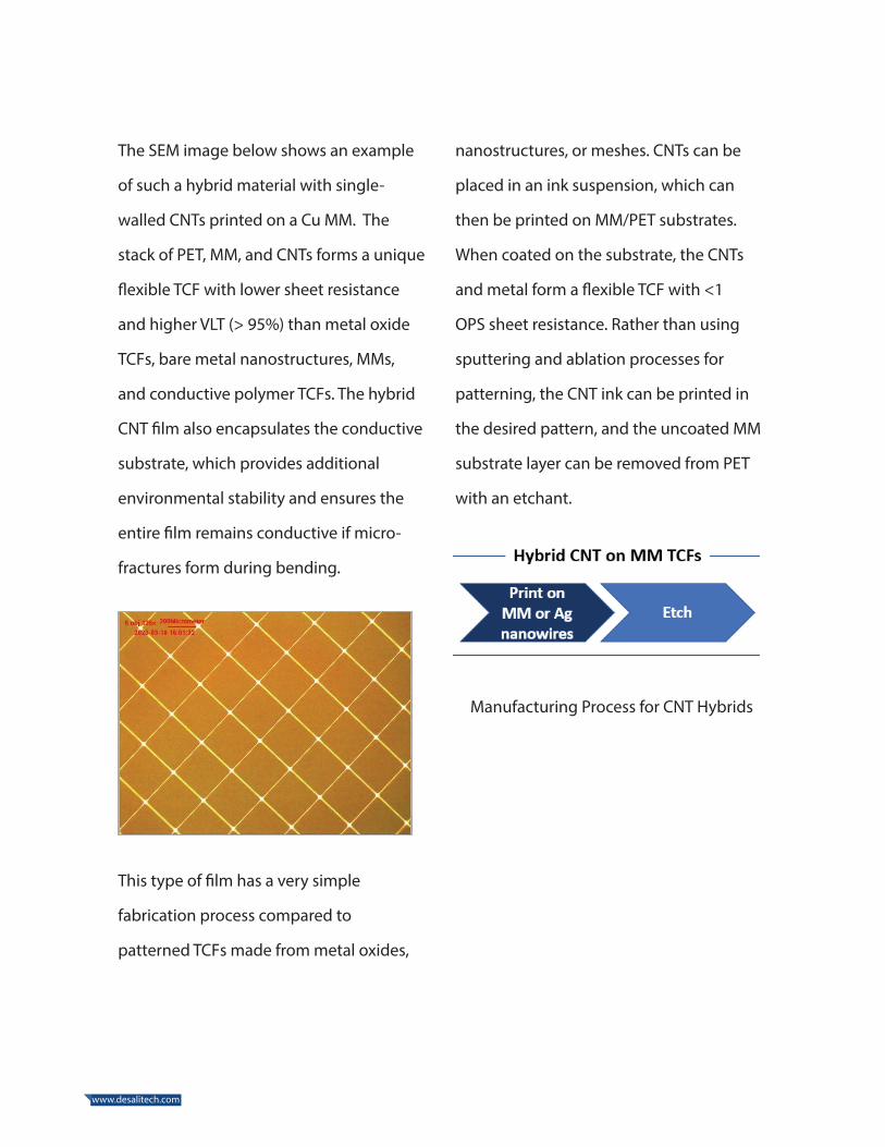
The SEM image below shows an example
of such a hybrid material with single-
walled CNTs printed on a Cu MM. The
stack of PET, MM, and CNTs forms a unique
flexible TCF with lower sheet resistance
and higher VLT (> 95%) than metal oxide
TCFs, bare metal nanostructures, MMs,
and conductive polymer TCFs. The hybrid
CNT film also encapsulates the conductive
substrate, which provides additional
environmental stability and ensures the
entire film remains conductive if micro-
fractures form during bending.
This type of film has a very simple
fabrication process compared to
patterned TCFs made from metal oxides,
nanostructures, or meshes. CNTs can be
placed in an ink suspension, which can
then be printed on MM/PET substrates.
When coated on the substrate, the CNTs
and metal form a flexible TCF with <1
OPS sheet resistance. Rather than using
sputtering and ablation processes for
patterning, the CNT ink can be printed in
the desired pattern, and the uncoated MM
substrate layer can be removed from PET
with an etchant.
Manufacturing Process for CNT Hybrids
www.desalitech.com
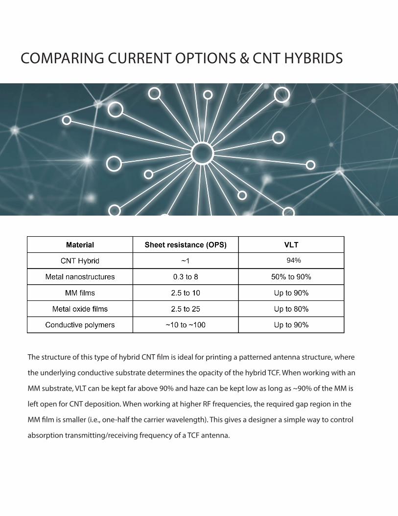
The structure of this type of hybrid CNT film is ideal for printing a patterned antenna structure, where
the underlying conductive substrate determines the opacity of the hybrid TCF. When working with an
MM substrate, VLT can be kept far above 90% and haze can be kept low as long as ~90% of the MM is
left open for CNT deposition. When working at higher RF frequencies, the required gap region in the
MM film is smaller (i.e., one-half the carrier wavelength). This gives a designer a simple way to control
absorption transmitting/receiving frequency of a TCF antenna.
COMPARING CURRENT OPTIONS & CNT HYBRIDS
94%
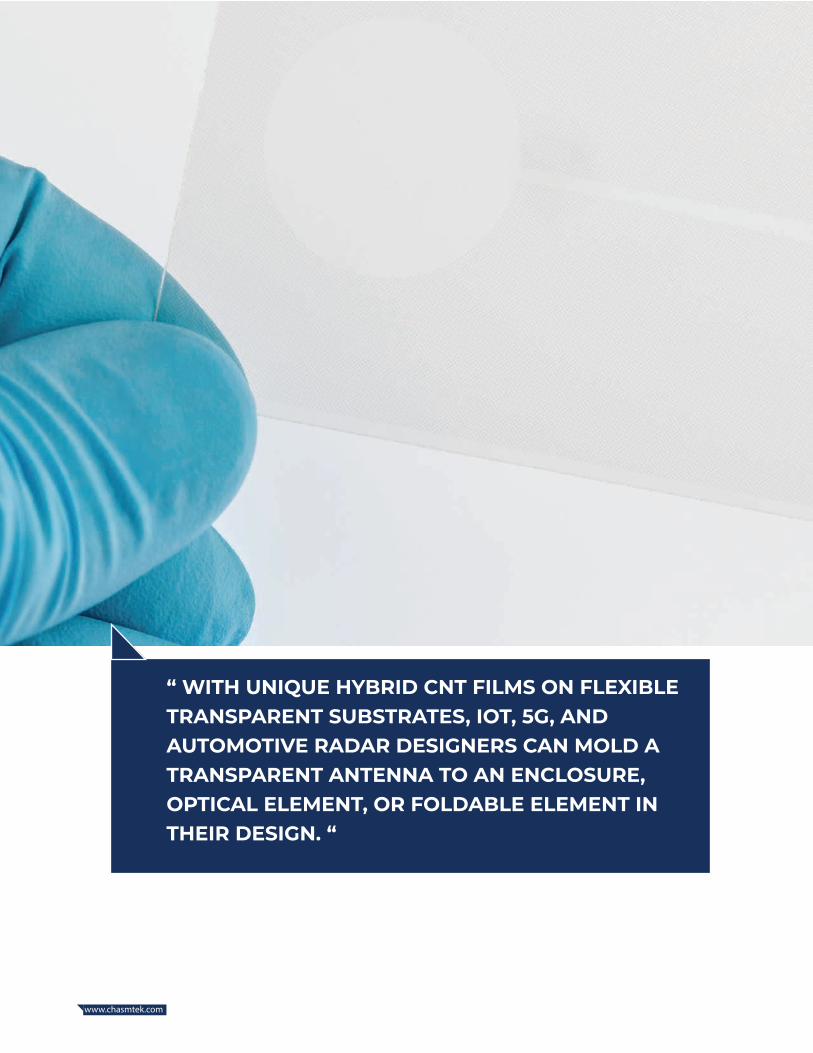
“ WITH UNIQUE HYBRID CNT FILMS ON FLEXIBLE TRANSPARENT SUBSTRATES, IOT, 5G, AND AUTOMOTIVE RADAR DESIGNERS CAN MOLD A TRANSPARENT ANTENNA TO AN ENCLOSURE, OPTICAL ELEMENT, OR FOLDABLE ELEMENT IN THEIR DESIGN. “
www.chasmtek.com
BRINGING IT TOGETHER
With unique hybrid CNT films on flexible trans-
parent substrates, IoT, 5G, and automotive radar
designers can mold a transparent antenna to an
enclosure, optical element, or foldable element
in their design. For IoT and 5G applications,
designers can tailor the emission pattern and
directionality through the use of a flexible TCF
and transparent FSS as a flexible substrate. For
radar, designers can create integrated optical/RF
sensors as these transparent antenna materials
could be molded onto optical devices, such as
cameras and lidar systems.
This hybrid CNT solution gives designers a flex-
ible transparent antenna that can be mounted
anywhere on the device, including directly on a
PCB. It also gives antenna designers the ability
to tailor the bandwidth, resonance structure,
directionality, and other antenna characteris-
tics while preserving high VLT with low sheet
resistance. Next-generation 5G-capable IoT and
automotive products need advanced antenna
designs that can only be provided by hybrid
CNT TCFs.
FORWARD TO A FRIEND>

Your Solutions, Our Materials.
WWW.CHASMTEK.COM
STAY IN TOUCH480 Neponset Street, Building 6Canton, MA
+1 781 989 [email protected]