transmitting, receiving, and interpreting...
TRANSCRIPT

TRANSMITTING, RECEIVING,
AND INTERPRETING ECG SIGNALS 6.101 FINAL PROJECT REPORT – SPRING 2015
DANIEL MOON & THIPOK (BEN) RAK-AMNOUYKIT
Abstract
We have designed and implemented a radio-frequency transmitter and a corresponding receiver capable of transmitting ECG signal, using a carrier frequency in the AM frequency band, over a distance up to 10 feet. At the receiver, a beat-detector circuit displays detected heartbeats with audible tone. The transmitter system is portable and powered by a 9V battery. It uses an n-channel JFET to modulate the amplitude of the carrier waveform with ECG signal. The amplitude-modulated signal is amplified, then transmitted via a solenoid antenna. Meanwhile, a stationary superheterodyne receiver obtains the AM signal and demodulates it with the help of a tuned local oscillator. The demodulated signal passes through intermediate-frequency (IF) stages. An auto-gain-control mechanism maintains a constant magnitude for the output. Finally, the recovered signal enters a series of amplification stages and is processed by the beat detector. The detector displays heartbeat by switching on the speaker and mimics the beating sound. The project explores a possibility for wireless patient monitoring using fundamental analog design principles.

2
TABLE OF CONTENTS
1. Overview 3 2. High-Level Block Diagram 4 3. Transmitter Modules 6
A. ECG Conditioning Circuit 7 B. Oscillators 9 C. Amplitude Modulation 13 D. Resonator 16
4. Receiver Modules 19 A. Superheterodyne Receiver 19 B. Peak Detector 25
5. System Integration and Testing 27 6. Review and Recommendation 28 7. Conclusion 29 8. Appendix 30
A. Full Circuit Schematic

3
1 Overview [Daniel]
An Electrocardiogram (ECG) is a device that records the electrical activity of a patient’s heart, with the use of electrodes and a circuit that filters and amplifies the heart rate signal. Typically, ECG devices are connected to patients who reside in stationary beds. The ECG signal is transmitted via wires to a bedside display, where a doctor can view and administer diagnosis. Therefore, checking ECG signal can be inconvenient for a patient who may want to move around while still being monitored. With the help of radio frequency transmission and amplitude modulation, a patient can transmit their heart signal from a mobile device to a stationary receiver, where the signal is processed and displayed. Our project aims to improve the wired, fixed-length configuration of the electrocardiogram to a potentially more mobile and wireless solution, where electrocardiography can occur within a distance of a wireless receiver.
To build our wireless AM-band ECG system, we start from two ECG electrodes on the user. A processing circuit captures the voltage difference, filters out noises, and amplifies the signal. A transmitting circuit modulates the signal with the carrier wave, whose frequency is in the AM broadcast band (from 535kHz to 1.7MHz). The receiver system demodulates the AM signal and filters out noise from the modulation stage. The output of the receiver system becomes the input of the sensor circuit that detects the ECG waveform and generates a beeping sound when a heartbeat is detected.
This report introduces our approach with a high-level block diagram, which covers the top-level implementation and explains general design decisions. The design decisions and calculations are emphasized in greater details in the module section. The transmission system contains four modules, while the receiver system contain two. For each individual module, we describe the calculations and steps we have taken to arrive at our design decisions. Lastly, we revisit the overall system, explain any issues that we have experienced and resolved during system testing, as well as comment on possible improvements for the project.

4
2 High-Level Block Diagram [Thipok]
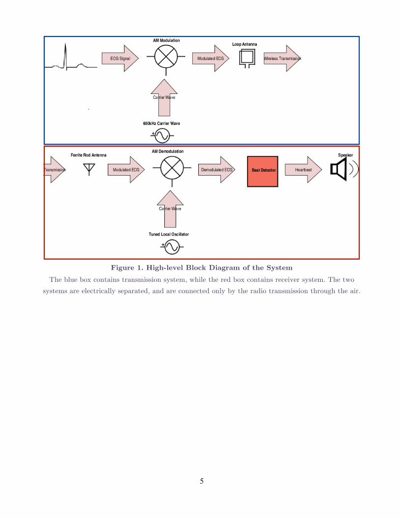
The complete system that transmits, receives, and interprets ECG signal can be divided into two separate smaller systems. They are connected only through the radio-frequency transmission over the air. The transmission system, in the blue box, covers everything from the electrodes on the user’s skin to the transmitting antenna. Ideally, this system should be portable and wearable by the user whose ECG signal is monitored. The receiver system, in the red box, covers everything from “picking up” the signal in the air to display the heartbeat with a speaker. It can be stationary and has fewer constraints for size and weight.
In the transmission system, we obtain the ECG signal from two electrodes on the user’s body. The signal becomes an input to an ECG processing circuit. Meanwhile, an oscillator circuit generates high-frequency sinusoidal waveform to serve as carrier wave for the AM transmission. The amplitude-modulating circuit uses the processed ECG signal to modulate the amplitude of the high-frequency carrier wave. The amplitude-modulated (AM) signal is then transmitted to the receiving station by a homemade antenna. Note that the portability of the transmission system doesn’t allow the use of large power supply. Therefore, every circuit in this system must be powered entirely by 9V battery.
The receiver system begins with a ferrite rod antenna, which responses to the AM signal in the air. The AM signal is mixed with another carrier wave from a tuned local oscillator, then demodulated by a series of subsystems known as “superheterodyne”. Once the original ECG signal is recovered, we have the option of displaying it on an oscilloscope to see the waveform. For a more tangible output, we use the recovered ECG signal as an input for the beat detector. The beat detector looks for peaks in the ECG signal that correspond to heartbeats and generates a beeping sound from the speaker for every beat it detects.
Simply speaking, the transmission and the receiver systems bring the ECG signal from your skin to the speaker. As your heart beats, the speaker beeps.
5
Figure 1. High-level Block Diagram of the System
The blue box contains transmission system, while the red box contains receiver system. The two systems are electrically separated, and are connected only by the radio transmission through the air.

6
3 Transmitter Modules [Thipok]
The transmitter modules cover everything from the two electric probes on the subject body to the transmitting antenna. It can be divided to four parts: an ECG conditioning circuit, an oscillator that generates constant AM carrier frequency, an amplitude modulation that combined the ECG signal and the carrier signal, and a resonator that amplified the amplitude modulated signal to the transmitting antenna.
Section 3-A discussed how the ECG conditioning circuit processes the input signals from two electrodes, removes the DC offset, filters out noises, and amplifies the signal. Section 3-B and section 3-C discuss how the oscillator generates a transmission carrier with constant frequency and how a JFET amplitude-modulate this carrier frequency with the processed ECG signals to obtain the AM signal. Section 3-D described a BJT circuit that amplifies the AM signal to drives an LC resonator where the transmitting antenna is located.
Also, note that the transmission half of the system is ideally portable. Therefore it must be designed to take power from a 9V battery and not from a desktop power supply. A typical circuit system needs positive power rail, negative power rail, and ground. With a 9V battery, we connect a voltage divider between the battery’s 2 electrodes. The battery’s positive electrode is set as the positive rails. The battery’s negative electrode as the negative rail. And the midpoint bias as the “virtual” ground for the rest of the system. One sufficiently large coupling capacitor (0.1uF) is placed between the battery’s electrodes. The other coupling capacitor is placed between the virtual ground and the negative rail.
Figure 2. Circuit Schematic of Power Rails
The transmission system is portable and powered by a 9V battery. For any circuit within the transmission system, we treat the battery’s positive electrode as the positive power rail, negative
electrode as the negative power rail, and midpoint bias as the virtual ground.
7
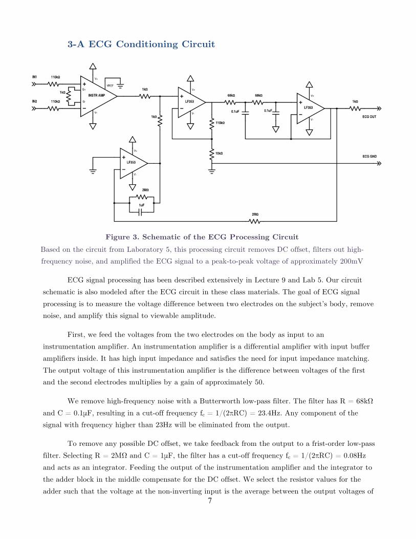
3-A ECG Conditioning Circuit
Figure 3. Schematic of the ECG Processing Circuit Based on the circuit from Laboratory 5, this processing circuit removes DC offset, filters out high-frequency noise, and amplified the ECG signal to a peak-to-peak voltage of approximately 200mV
ECG signal processing has been described extensively in Lecture 9 and Lab 5. Our circuit schematic is also modeled after the ECG circuit in these class materials. The goal of ECG signal processing is to measure the voltage difference between two electrodes on the subject’s body, remove noise, and amplify this signal to viewable amplitude.
First, we feed the voltages from the two electrodes on the body as input to an instrumentation amplifier. An instrumentation amplifier is a differential amplifier with input buffer amplifiers inside. It has high input impedance and satisfies the need for input impedance matching. The output voltage of this instrumentation amplifier is the difference between voltages of the first and the second electrodes multiplies by a gain of approximately 50.
We remove high-frequency noise with a Butterworth low-pass filter. The filter has R = 68kΩ and C = 0.1μF, resulting in a cut-off frequency fc = 1/(2πRC) = 23.4Hz. Any component of the signal with frequency higher than 23Hz will be eliminated from the output.
To remove any possible DC offset, we take feedback from the output to a frist-order low-pass filter. Selecting R = 2MΩ and C = 1μF, the filter has a cut-off frequency fc = 1/(2πRC) = 0.08Hz and acts as an integrator. Feeding the output of the instrumentation amplifier and the integrator to the adder block in the middle compensate for the DC offset. We select the resistor values for the adder such that the voltage at the non-inverting input is the average between the output voltages of
8
the instrumentation amplifier and the integrator. This will give a gain of 1/2 to the signal. The adder gives an additional gain of (110kΩ+10kΩ)/10kΩ = 12. Therefore, the gain in this stage is 1/2 x 12 = 6.
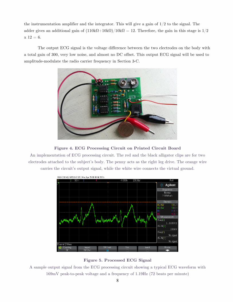
The output ECG signal is the voltage difference between the two electrodes on the body with a total gain of 300, very low noise, and almost no DC offset. This output ECG signal will be used to amplitude-modulate the radio carrier frequency in Section 3-C.
Figure 4. ECG Processing Circuit on Printed Circuit Board An implementation of ECG processing circuit. The red and the black alligator clips are for two
electrodes attached to the subject’s body. The penny acts as the right leg drive. The orange wire carries the circuit’s output signal, while the white wire connects the virtual ground.
Figure 5. Processed ECG Signal A sample output signal from the ECG processing circuit showing a typical ECG waveform with
169mV peak-to-peak voltage and a frequency of 1.19Hz (72 beats per minute)

9
3-B Oscillator
Figure 6. Circuit Schematic of the Carrier Frequency Generator
The sinusoidal carrier frequency for AM transmission is generated by cascading a Wien bridge oscillator with a Butterworth low-pass filter. The low-pass filter’s cut-off frequency must allow only the lowest
harmonic of the oscillator.
To send the ECG signal over the air using AM transmission, we must first generate the carrier wave. The carrier wave must be sinusoidal and has a frequency within the AM band. For this project, we may pick any frequency in the allowed range, because the laboratory has good shielding against AM broadcasting from radio stations. Originally, we tested our system at 560kHz, but decided to change the carrier frequency to 650kHz for a better signal at the superheterodyne receiver.
The carrier wave is generated by a Wien bridge oscillator. The oscillator’s inverting input behaves like an amplifier with positive gain. The non-inverting input is a bandpass filter providing positive feedback from the output. Assuming that the Op Amp has a very large gain, the oscillation requires that V+ = V-

10
Figure 7. Wien Bridge Oscillator
𝑉! = 1R + jωC
!!
𝑅 + 1jωC +
1R + jωC
!! V!"# = 1 + 1 + jωCR !
𝑗ωCR
!!
V!"#
V! = R!
𝑅! + 𝑅!V!"#
To satisfy this condition, we must have ωCR = 1 and R4 = 2R3
Given f = 650kHz and C = 10pF, we obtain R = 1/(2πfC) = 24.5kΩ. In our implementation, we select C = 10pF, R = 24 kΩ, R3 = 10 kΩ, and R4 = 22kΩ.
During the experiment, we notice two issues with the Wien bridge oscillator. First, a rail-to-rail Op Amp, such as LT1632, in this configuration draws relatively large current and causes oscillation in the power rails. Note that the power rails are the positive and negative electrodes of a 9V battery, not from a power supply. We solve this problem by replacing the LT1632 with LF356, which does not provide rail-to-rail output voltage but draws much less current. Still, because the values of resistors and capacitors in our Wien bridge oscillator are not ideal, the oscillator’s output turns out to resemble a square wave, rather than a sinusoidal wave in the ideal case. An example of such square waveform is shown in Figure 8.
To guarantee that the carrier wave is sinusoidal, we feed the oscillator’s output into a low-pass filter. Knowing that a square wave of frequency “fo” is an infinite sum of all harmonics of fo, we design our low-pass filter such that only the fundamental harmonic of fo is allowed. We choose a Butterworth filter, which provides flattest magnitude response at frequencies below the cut-off frequency.

11
Figure 8. Output of the Wien Bridge Oscillator The Wien bridge oscillator gives a square output waveform at a test frequency of 560kHz. The
square waveform contains many harmonics of the frequency 560kHz.
Figure 9. Butterworth Low-Pass Filter
A Butterworth low-pass filter is a second-order filter with maximally flat magnitude response.
The transfer function of the Butterworth filter above is
T jω = 𝑉!"#(jω)𝑉!"(jω)
=1
1−ω!R!C!C! + j(2ωRC!)
T jω = 1−ω!R!C!C! ! + 2ωRC! ! !!/!
We would like a flat response function at ω = 0.
𝑑 T jω
𝑑ω!!!
= 0 → C! = 2C!

12
With C3 = 2C4, |T(jω)| becomes T jω = 1+ 4 ωRC! ! !!/!. The cut-off frequency is
ω! = 12𝑅𝐶!
→ f! = 1
2 2π𝑅𝐶!
To retain only the fundamental frequency of the square waveform, the filter must have a cut-off frequency f = fo = 650kHz. Choosing C4 = 22pF, we calculate R = 7.87kΩ. As a design decision, we use R = 8.2kΩ, C4 = 22pF, and C3 = 47pF. The filter’s output is a clean sinusoidal waveform, as shown in the Figure below.
Figure 10. Output of the Butterworth Low-Pass Filter The Butterworth low-pass filter takes in the Wien bridge oscillator’s square output waveform and
filters out all but the lowest harmonic, resulting in the sinusoidal waveform at 560kHz.

13
3-C Amplitude Modulation
Figure 11. Schematic of the Amplitude Modulation Circuit
The ECG signal from the processing circuit is amplified and fed to the gate of an n-channel JFET. The JFET is in common-source configuration and gives the amplitude-modulated signal at its drain
terminal. Resistors in the circuit are chosen such that the modulation is linear.
A critical part of the transmitter is the amplitude modulation. In this stage, the amplitude of the carrier wave is modulated by a time-varying signal. For example, if we have a carrier signal with a high frequency fo such that the carrier wave is vc(t) = Vo sin(2πfot), an amplitude modulation by the signal vs(t), whose frequency is significantly smaller, will give the AM signal:
vM(t) = A[Vo+bvs(t)] sin(2πfot)
where A is the gain and b is the modulation constant. In this project, vs(t) is the ECG signal.
The amplitude modulation is implemented with an n-channel JFET in common-source configuration. The small-signal output resistance ro of the JFET is a function of the large-signal gate-source voltage VGS. Assuming that the JFET is biased in saturation region, we the quiescent drain current is
𝐼! ≈ 𝐼!"" 1 −𝑉!"𝑉!
!= 𝐼!"" 1 +
𝑉!"|𝑉!|
!
where IDSS is the saturation current and VP is the pinch-off voltage. For a 2N5459 JFET, the typical value for IDSS is 9.0mA. VP is negative and usually between -2.0V to -8.0V.
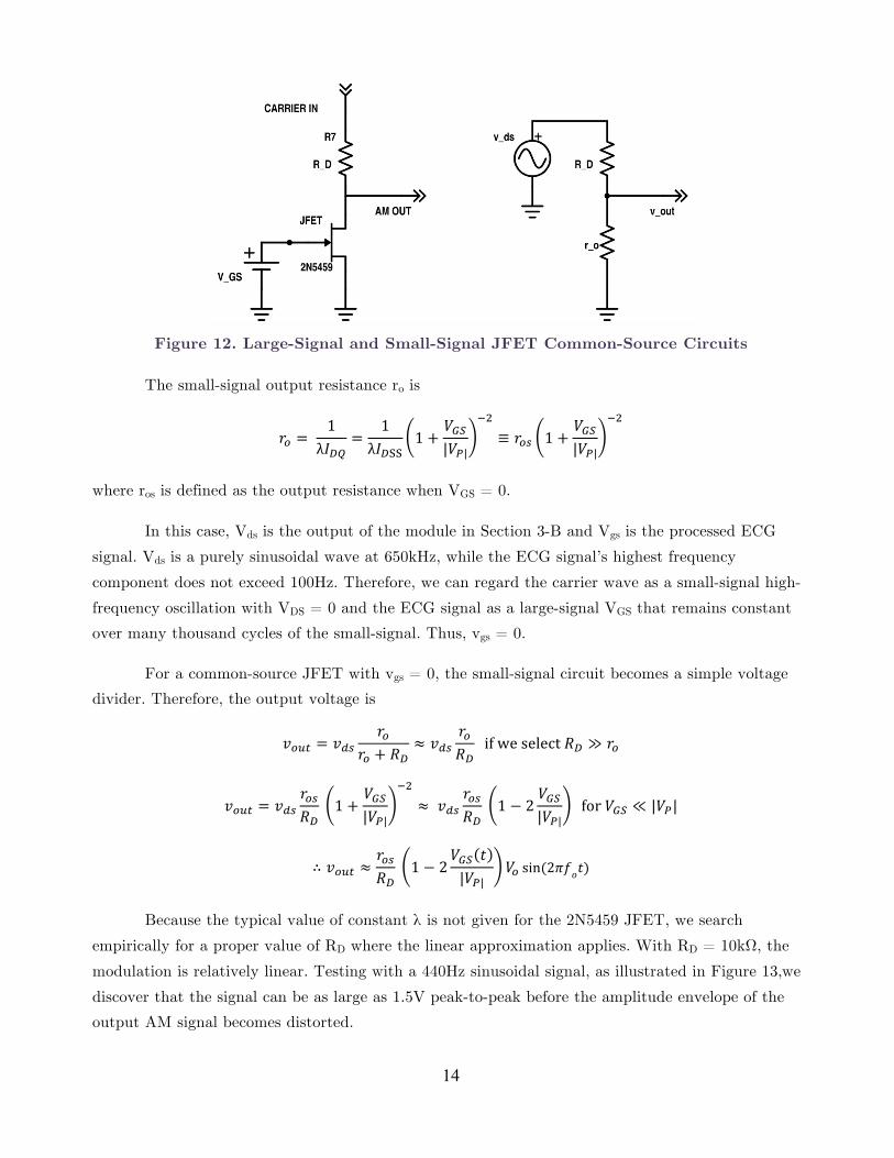
14
Figure 12. Large-Signal and Small-Signal JFET Common-Source Circuits
The small-signal output resistance ro is
𝑟! = 1
λ𝐼!"=
1λ𝐼!!!
1 +𝑉!"|𝑉!|
!!
≡ 𝑟!" 1 +𝑉!"|𝑉!|
!!
where ros is defined as the output resistance when VGS = 0.
In this case, Vds is the output of the module in Section 3-B and Vgs is the processed ECG signal. Vds is a purely sinusoidal wave at 650kHz, while the ECG signal’s highest frequency component does not exceed 100Hz. Therefore, we can regard the carrier wave as a small-signal high-frequency oscillation with VDS = 0 and the ECG signal as a large-signal VGS that remains constant over many thousand cycles of the small-signal. Thus, vgs = 0.
For a common-source JFET with vgs = 0, the small-signal circuit becomes a simple voltage divider. Therefore, the output voltage is
𝑣!"# = 𝑣!"𝑟!
𝑟! + 𝑅!≈ 𝑣!"
𝑟!𝑅!
if we select 𝑅! ≫ 𝑟!
𝑣!"# = 𝑣!"𝑟!"𝑅! 1 +
𝑉!"|𝑉!|
!!
≈ 𝑣!"𝑟!"𝑅! 1 − 2
𝑉!"|𝑉!|
for 𝑉!" ≪ |𝑉!|
∴ 𝑣!"# ≈𝑟!"𝑅! 1 − 2
𝑉!" 𝑡|𝑉!|
𝑉! sin(2𝜋𝑓𝑜𝑡)
Because the typical value of constant λ is not given for the 2N5459 JFET, we search empirically for a proper value of RD where the linear approximation applies. With RD = 10kΩ, the modulation is relatively linear. Testing with a 440Hz sinusoidal signal, as illustrated in Figure 13,we discover that the signal can be as large as 1.5V peak-to-peak before the amplitude envelope of the output AM signal becomes distorted.

15
Figure 13. A Sample of Amplitude Modulation with Sinusoidal Signal 660kHz carrier frequency is amplitude-modulated by 440Hz sinusoidal signal with 1.5V peak-to-peak
voltage. The resulting signal is still an oscillation with the frequency 660kHz, but has varying sinusoidal amplitudes controlled by the 440Hz input signal.
Knowing that the depth of modulation is directly proportional to the strength of demodulated signal at the receiver, our design decision is to amplify the ECG signal from Section 3-A such that its peak-to-peak amplitude is close to the linearity limit of about 1.5V. Referring back to the schematic in Figure 11, the ECG signal from Section 3-A is amplified by a gain of (10kΩ+2kΩ)/2kΩ = 6. The 20kΩ resistor limits the current flowing into the gate of the JFET.
The AM signal output at the drain of the JFET has a peak-to-peak amplitude of approximately 50mV. Since the output signal vout contains the term ro/RD, its small amplitude corresponds to the assumption that RD >> ro.

16
3-D Resonator
Figure 14. Circuit Schematic of the Resonator
The amplitude-modulated signal becomes an input to the left BJT, giving an output signal with unity gain at its emitter. This signal becomes an input signal to the right BJT. The BJT amplifies
the signal and drive the LC tank-circuit containing the transmitting antenna
The amplitude-modulated signal at the drain of the JFET is too small to drive the transmitting antenna. To isolate the amplitude modulating circuit from any effect from the amplifier, we first inputs the AM signal into a common-collector BJT. The left BJT in the schematic above has its collector connected directly to the positive power rail. The BJT’s base terminal is biased at the virtual ground – a midpoint between the positive and the negative rails – with a simple voltage divider. For small-signal model, a common-collector BJT has a unity gain, very large input impedance, and small output impedance. It acts almost as a voltage source with the voltage at its emitter equals to that of the AM signal.
The right BJT is in common-base configuration. As per convention, the collector impedance XC is defined as the impedance between the BJT’s collector and the positive power rail. The load resistance RL is defined as the resistance between the collector and the ground. For our circuit, XC can be derived from the capacitance C of the trimmer capacitor and the impedance L of the solenoid inductor. RL is infinite since there is no load. The small-signal voltage gain for common-base configuration is
𝐴! = 𝑔!(𝑋!| 𝑅! = 𝑔!𝑋!
At a given frequency ω, the collector impedance XC is

17
𝑋! 𝑗𝜔 =
1𝑗𝜔𝐶 ∙ 𝑗𝜔𝐿
1𝑗𝜔𝐶 + 𝑗𝜔𝐿
=𝑗𝜔𝐿
1 − 𝜔!𝐿𝐶
We notice that at the resonance frequency ωo where ωo2 = LC, the impedance XC(jω)
approaches infinity. Consequently, the small-signal voltage gain also approaches infinity. When the resonator circuit is tuned well, our AM signal with approximately 50mV peak-to-peak voltage seems to be amplified with infinite gain!
In reality, we do not achieve the infinite gain. First, the maximum peak-to-peak voltage of the collector voltage is limited by the power rails. It will not exceed 9V. Moreover, the clipping effect when the gain is too large will distort the envelope of the AM waveform, thus distort the demodulated ECG signal at the receiver. We tune the variable capacitor such that the tank circuit’s resonance frequency is close to, but not exactly the 650kHz carrier frequency of our AM transmission.
Figure 15. Transmitting Antenna The transmitting antenna is a solenoid with 1-foot x 1-foot square frame. The antenna has an
inductance of approximately 600μH.
There are two main types of transmitting antenna - the physically resonant antenna and the physically small antenna. The physically resonant antenna requires the antenna length to be a multiple of λ/4. It is sometimes known as the “quarter-wave” antenna. However, for f = 650kHz, we can calculate λ/4 = c/4f = 115m. For our carrier frequency, even the minimum length for a resonant antenna is even taller than the department building. The physically small antenna is basically a solenoid. The signal strength is directly proportional to the magnitude of magnetic field the solenoid generates. In the first trial, we built a 4-inch by 4-inch solenoid antenna with an inductance of 60μH.

18
Even when tested with a commercial AM radio receiver, the antenna can transmit up to only 3 to 4 feet. To reach the goal of 10-foot transmission, we built a new 1-foot by 1-foot solenoid with an inductance of 600μH. Although the new antenna gives strong and clear signal, its size makes the transmission system no longer portable. We may fit all modules in a small PCB, but no one will want to carry around a 1-foot by 1-foot solenoid just to transmit his/her ECG signal.
Figure 16. ECG Signal and its Amplitude-Modulated Signal A comparison between amplified ECG signal with 1.53V peak-to-peak voltage and the amplitude-
modulated ECG signal measured at the transmitting antenna.

19
4 Receiver Modules [Daniel]
4-A Superheterodyne Receiver
Figure 17. Circuit Schematic of Superheterodyne Receiver
A Superheterdyne receiver was used to receive the AM modulated ECG signal. Super-heterodyne receivers are the staple of modern radio receivers providing the best form of reception, selectivity and sensitivity. This along with a large repository of guides on superheterodyne radio building is why we chose this design for our receiver. Superheterodyne receivers are receivers that convert a carrier wave of interest down to an intermediate frequency (IF), typically 455kHZ which is the process called heterodyning, where filtering and amplification occurs. Amplifying at this IF occurs because it is a standard IF frequency, making it easy to make parts which operate specifically at this frequency and since lower frequency transistors have better gain than its RF components. All of these frequencies are above the frequency spectrum of hearing, which is where the superheterodyne (contraction for Supersonic heterodoyne) comes from.
Our Superheterodyne receiver is modeled after the 536 AM radio kit from Graymark. Although many other solutions with detailed structures were present, we decided to go with this implementation as it had defined stages of the entire process and gave a good informative understanding of how the entire receiver process operated.
The Superheterodyne receiver has four primary stages. The shifting of the AM signal to IF using a local oscillator, IF amplification stages, auto-gain detection and an audio amplifying stage.
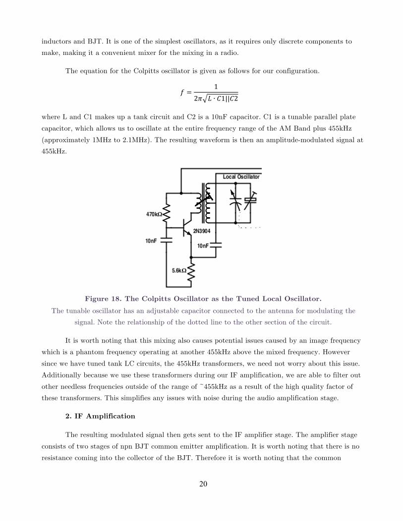
1. Local Oscillator
The local oscillator which mixes the received AM signal down to the IF stage is a Colpitts oscillator. The Colpitts oscillator is an oscillator configuration that primarily uses capacitors,
20
inductors and BJT. It is one of the simplest oscillators, as it requires only discrete components to make, making it a convenient mixer for the mixing in a radio.
The equation for the Colpitts oscillator is given as follows for our configuration.
𝑓 =1
2𝜋 𝐿 ∙ 𝐶1||𝐶2
where L and C1 makes up a tank circuit and C2 is a 10nF capacitor. C1 is a tunable parallel plate capacitor, which allows us to oscillate at the entire frequency range of the AM Band plus 455kHz (approximately 1MHz to 2.1MHz). The resulting waveform is then an amplitude-modulated signal at 455kHz.
Figure 18. The Colpitts Oscillator as the Tuned Local Oscillator.
The tunable oscillator has an adjustable capacitor connected to the antenna for modulating the signal. Note the relationship of the dotted line to the other section of the circuit.
It is worth noting that this mixing also causes potential issues caused by an image frequency which is a phantom frequency operating at another 455kHz above the mixed frequency. However since we have tuned tank LC circuits, the 455kHz transformers, we need not worry about this issue. Additionally because we use these transformers during our IF amplification, we are able to filter out other needless frequencies outside of the range of ~455kHz as a result of the high quality factor of these transformers. This simplifies any issues with noise during the audio amplification stage.
2. IF Amplification
The resulting modulated signal then gets sent to the IF amplifier stage. The amplifier stage consists of two stages of npn BJT common emitter amplification. It is worth noting that there is no resistance coming into the collector of the BJT. Therefore it is worth noting that the common
21
emitter amplifier is not used as a voltage amplifier but as a current amplifier. Therefore the equation for current gain is
𝑖!𝑖!= −𝑔!(𝑟!||𝑅!)
Since the resistance coming into the base of the BJT is much bigger than internal resistance from the base to the emitter rπ . Therefore,
𝑖!𝑖!≈ −𝑔! 𝑟! = −𝛽
As such, we noticed that current gain is based solely on the ratio of DC collector current to the DC base, beta. Since the transformer 4:1 turn ratio the current through the secondary winding will be ¼ of the current going through the primary winding. As a result, the current after the second stage and the additional transformer stage going into the auto gain detector is !!!!
!".
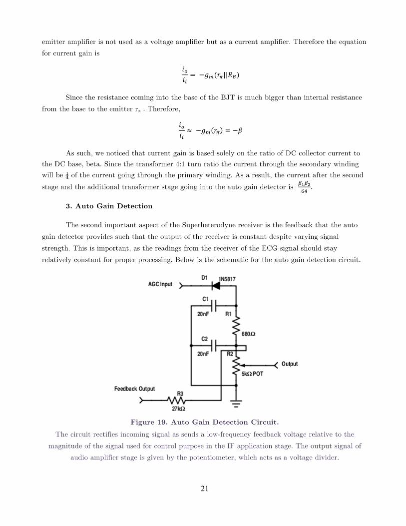
3. Auto Gain Detection
The second important aspect of the Superheterodyne receiver is the feedback that the auto gain detector provides such that the output of the receiver is constant despite varying signal strength. This is important, as the readings from the receiver of the ECG signal should stay relatively constant for proper processing. Below is the schematic for the auto gain detection circuit.
Figure 19. Auto Gain Detection Circuit.
The circuit rectifies incoming signal as sends a low-frequency feedback voltage relative to the magnitude of the signal used for control purpose in the IF application stage. The output signal of
audio amplifier stage is given by the potentiometer, which acts as a voltage divider.
22
Diode D1, 1N5817, C1 and R1 act as a half-wave rectifier and rectifies the negative portion of the signal. Recall that the ratio of voltage ripple to the full voltage is:
𝑉!"##$%𝑉!
=1𝑓𝑅𝐶
Where 𝑉!"##$% is the peak-to-peak voltage of the ripple and 𝑉! is the amplitude of the signal. Since we are operating at the IF frequency of 455kHz, Vripple is roughly 16% of the entire amplitude of the signal. As such, 92% of the signal’s peak value is present at the bottom terminal of R1 making it a reasonable rectifier. This voltage is then passed through R3 and is the bias voltage for the Mixer BJT and the BJT of the first amplification stage. Since the frequency of the bias voltage is in the spectrum the, bias voltage is not pulled down by the capacitors. This bias can control the gain of each IF stage. For example if a large input signal is rectified, a large negative voltage will be fed to the base of the two BJTs reducing the base voltage of the amplifiers which reduce the amplifier gain in order for the incoming to be reduced and stay at similar voltage level. Essentially, the base voltage varies the emitter current, which varies 𝛽 and therefore varies the amplifier gain. With this control, we can create a constant volume control and have the ECG wave form to have constant peaks.
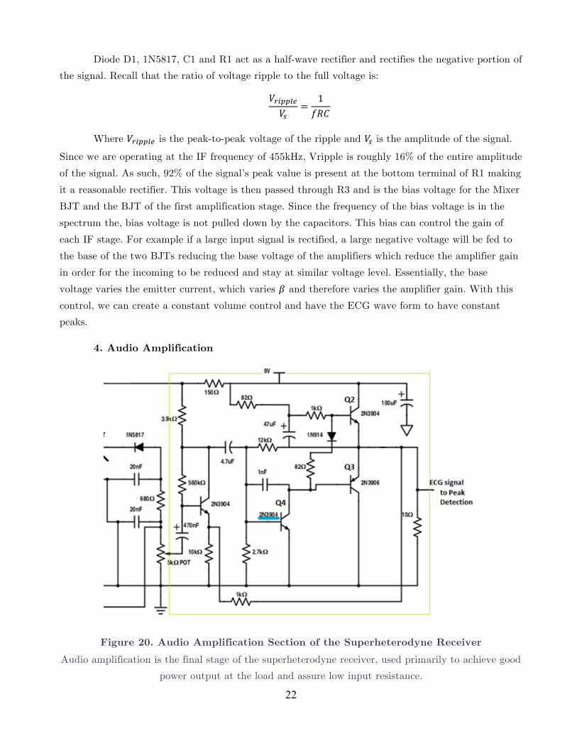
4. Audio Amplification
Figure 20. Audio Amplification Section of the Superheterodyne Receiver
Audio amplification is the final stage of the superheterodyne receiver, used primarily to achieve good power output at the load and assure low input resistance.

23
The input to audio amplification stage comes from the potentiometer which selects the voltage of the signal at different voltage levels. The gain of the first BJT amplifier, Q1, varies as it depends on the negative feedback of the final stage of amplification through the 1kΩ resistor which is in parallel with the 10kohm resistor to ground. The voltage output from the AGC is on the order of volts, but due to the high impedance, there is very little current leading to very small power to drive the 10Ω sense resistor which will have the ECG waveform. We solve this issue by creating an audio amplifier with low output impedance to match the low resistance of the sense resistor.
The first stage amplifier, Q1, with its voltage input from the potentiometer is a class A amplifier. This amplifier provides enough voltage and power gain to drive the push pull transistors, Q2 and Q3 in the following stage. This amplifier stage is an AB amplifier stage. During the positive swing of the audio signal, the npn BJT Q2 will conduct and the pnp BJT Q3 conducts during the negative swing of the audio signal. The 1N914 diode allows for conduction for each of the BJTs to occur at separate voltage ranges. This is important since activation of both transistors will cause a large current flow through both. Thus the halfway idle bias voltage is done by the following.
Q2 is biased by the current produced by 82Ω resistor and 1kΩ resistor. If no other circuit elements are present, the bias current will cause the BJT emitter to rise to 9 V minus the Collector-Emitter voltage drop. This is prevented by connecting the 12k resistor between the emitter of Q2 to the base of Q4. As a result when a higher bias current is applied to Q2, the collector emitter resistance becomes smaller. The collector of Q4 is connected by the diode and 82 ohm resistor in series to the base of Q2 of the push pull. When Q4 decreases in intrinsic resistance it pulls more current from Q2 which therefore increase the collector emitter resistance of Q2. This network essentially reduces to a voltage divider. We can now go back to Q3, the pnp of the push pull. Q3 conducts when base-emitter junction is forward biased. It can also not conduct at the same time as Q2 as mentioned earlier.
The 4.7μF capacitor couples the audio signal to the base Q4. When there is a positive output swing, Q4 will conduct more. As a result, Q3 conducts more as well. Simultaneously, current is pulled from the base of Q2 to Q4 and therefore Q2 conducts less. On the negative swing of the signal. Q3 conducts less, leading to Q4 to reverse bias. As a result more current is driven to the base of Q2 which allows it to conduct more. As a result of this audio amplifier stage, we have a low output impedance circuit which power a low impedance load with minimal distortion.

24
Figure 21. Superheterodyne Receiver on Printed Circuit Board and Its Speaker

25
4-B Peak Detector
The peak detector circuit is the processing end of our final project where we process the received ECG signal from our superheterodyne receiver and output an audible beep from a speaker to indicate a heartbeat. The detector consists of a rectifying stage, a comparator stage which acts as an analog switch for the beep generation, and a Wien bridge oscillator for the tone of the beep.
Figure 22. Circuit Schematic of the Peak Detector The peak detector takes in the demodulated ECG waveform, detects peak, and outputs the result as
tonal beeps corresponded to the user’s heartbeats.
1. Rectifying Stage The rectifying stage of the peak detector stage consists of two stages of precision rectification and a unity gain buffer. I chose to use the LT1632, although any jellybean op amp would do as ECG waveforms compose of frequencies from a range of 1- 100Hz and our voltage output from the Superheterodyne receiver is at least almost 1 V in magnitude. I chose to use precision rectifiers to avoid any attenuation, which may lead to failure in detection of heart beats. A precision rectifier is a diode configuration in which a signal is wired to the positive input and the negative terminal is connected to cathode of a diode at the output of the op-amp as shown in the figure. The voltage drop of a precision rectifier, or super diode, is very close to 0. It’s voltage drop is equal to voltage drop of the diode which is about 0.7V for the 1N914 diode divide by the open loop gain of the op amp which is typically 4000 for the LT1632. Therefore we can approximate the voltage drop through a super diode to be 0V. Using the precision rectifier a built a two stage wave rectifiers with

26
the assumption that an ECG could be approximated as a half wave signal. I also assumed that for an average patient, their heart rate will range from 0.8Hz to 3Hz. As such I used a 1mF capacitor and a 100kΩ resistor to design a half wave rectifier with a ripple voltage 6.7% of the total amplitude of the signal at 1.5Hz. In reality however, the ripple was about 20% of the actual amplitude of the signal so another stage was made, which resulted in a ripple that was about 7% of the amplitude of the original signal. Therefore the average DC value of the output of the rectifier stage was nearly the original peak value of the signal. A unity gain buffer stage was added to isolate the previous impedances in the rectifying stage from affecting the comparator stage.
2. Comparator Stage The comparator stage of the peak detector checks if the voltage of the ECG waveform is at least larger than 75% of the peak value of the ECG and will switch an n-channel JFET open allowing oscillation generator to be fed into speaker allowing the beeping to occur.
The output of the rectifier stage gets reduced to 75% of its value by a resistor divider stage by the 10kohm and 30kohm resistors in series. The reduced signal is then fed to the negative port of a op amp comparator and the ECG signal from the receiver is fed to the positive port. This comparator switches to +5 volts when the ECG signal is greater than 75% of its peak value and 0 otherwise. This signal is then fed through an inverting amplifier with a gain of -1. This inversion is needed for the correct operation of the JFET. The n-channel JFET, 2N5459 has a typical cut off around -5V. The 2N5459 had a cutoff of VGS(off)= -4V. Essentially if VGS is less than VGS(off) the FET is in cut off and does not conduct current from drain to source, acting as an open current. This allows the sound from the oscillation generator to go through to a unity gain buffer to isolate other impedances and have the speaker produce a tone. When VGS is greater than VGS(off), the FET turns on and generates a current from drain to source. Therefore FET acts as a closed circuit with very small resistance. This will pull down the oscillation and prevent a tone from appearing from the output of the speaker.
3. Sound Generation Lastly, the oscillation which generates the beeping frequency is a Wien bridge oscillator. As mentioned in Section 3-B, the Wien bridge oscillator is an op amp circuit that can create an oscillation at a given frequency when the resistance and capacitance values are equal for the parallel RC component from the positive terminal to ground and the series RC circuit from plus terminal to output as well as the frequency specified equals !
!!"#. One 11kΩ resistor and one 30nF capacitor
resulted in a tone very close to a center A. Also, although LT1632 clips when using this oscillator configuration, because we perceive pitch by oscillation rather than smoothness of the wave, the tone still resembled middle “A” and was a good pitch for the beat detector circuitry.
27
5 System Integration and Testing [Thipok]
System integration does not cost as much issues as expected. Generally, if each individual module works well by itself, combining two modules together will not bring up any problem as far as they are properly “isolated” from each other. For example, placing a voltage-follower with high input impedance and low output impedance at the junction between two different modules help shield each circuit from affecting the other. However, because both the transmitting and the receiver system involve oscillator and resonator circuits, the most important issue for system integration is tuning.
System testing starts from the most important module – the amplitude modulation. In addition to testing with simulation program such as LTSpice, we determine the optimal values for gate and drain resistors experimentally. Using a 440Hz sinusoidal signal, we try many resistance values, display the resulting AM signal between the drain and the source of the JFET, and compare their performance.
With the amplitude modulation functioning effectively, we move on to testing the resonator circuit. We use Prof. Hom’s commercial handheld AM radio as a standard for the measurement of each antenna’s transmitting power. We still uses a 440Hz sinusoidal signal for testing purpose, because the handheld radio speaker is more responsive to at this frequency than the typical frequency range of ECG signal. We tune each LC tank circuit to reach its maximum transmitting power, and measure the furthest distance at which the handheld radio is still able to pick up the 440Hz sinusoidal signal. In this stage, we discover that the solenoid antenna needs to be relatively large to transmit the signal over 10 feet, possibly due to the ineffectiveness of non-resonant antenna. At a fixed transmitting distance, we also discover that the peak-to-peak amplitude of the signal can be as large as 1.5V before the linearity assumption during amplitude modulation is no longer valid.
We tune the LC resonator for maximum performance given a sinusoidal signal with frequency between 400-800Hz. Upon broadcasting actual ECG signal using the same setting, we notice that the it is significantly more difficult for the handheld radio to pick up the ECG signal than the audio-frequency sinusoidal signal. This difficulty is due to the difference in characteristics between the ECG and the audio signals.
For the receiver system, the test for superheterodyne receiver is simple. With proper tuning, we expect that it is able to pick up radio signal from broadcasting AM stations. The test for peak detector is also relatively simple. We use a function generator to generate cardiac-like pulses with the frequency of 1Hz. Feeding the pulse train as input to the beat detector circuit, we expect to hear the speaker beeping at the rate of 1Hz. Note that 1Hz must be the speaker’s beeping rate, not the frequency of the beeping tone.
28
Once all modules in both the transmission and the receiver systems are working, we test the overall system by connecting one of the two project members to the ECG circuit and broadcast the AM signal with the antenna. If everything functions properly, we should be able to hear the heartbeat from the receiver’s speaker. From the testing, we realize that the superheterodyne receiver is less receptive to the ECG signal and that we can best achieve the transmission distance of only 2 – 3 feet.
6 Review and Recommendation [Daniel]
The project meets most of the expected goals, but falls short on the stretch goals. The system is not portable, because a large antenna is required for a transmission over 10 feet to a handheld radio receiver. The transmission distance is even shorter for the transmission to the homemade superheterodyne receiver. Nevertheless, the superheterodyne receiver has an auto gain control. Other that the goals stated in the project checklist, over the course of the project we have noticed a few issues that we would like to address if we had some additional time.
First, we use integrated circuit rather inefficiently in many circuits. That is, same
functionality in some circuits can be achieved with discrete components, such as resistor, capacitor, BJT, and FET, rather than the IC chips such as operational amplifiers. From the consumer electronic perspective, we would like our design to contain fewer integrated circuits to reduce the cost. For example, instead of using an Op-Amp oscillator, we could have built a phase-shift oscillator from only BJTs, resistors, and capacitors. Also, instead of using an Op-Amp as a voltage buffer, we could have considered using a BJT in common-collector configuration as an emitter-follower. Especially for the beat-detection module, the project could have been more challenge if we design the circuit with the idea of relying more on the discrete components.
Another possible point for improvement is to design the radio-frequency transmission in FM
band, instead of the AM. There are many good resources for FM transmitters and receivers. Frequency modulation offers higher fidelity, as well as more bandwidth reserved for amateur radio. Even though building frequency modulation and frequency demodulation circuits with discrete components could be a great challenge, it might have been a better implementation for the project. We might be able to transmission over longer distance and experience less noise.
It is also a good idea to revisit and re-design the beat detection circuit. Because the ECG signal from the demodulation stage is very noisy, we could have improved the comparator circuit by replacing the JFET switch with an Op-Amp comparator that has hysteresis characteristic. If we set a noise threshold around the voltage being compared, we might receive clearer beeping, rather than hearing bouts of buzzing.

29
7 Conclusion
The “Transmitting, Receiving, and Interpreting ECG Signal” project is a great opportunity for us to design and implement analog circuits based on 6.101’s class materials and lab assignments. We also do additional researches on amplitude modulation and demodulation. During the implementation and experimentation stages, we learn that the behaviors of a physical system can deviate greatly from its simulation result. Understanding this difference is an essential step for every analog design engineers. In the end, we are able to meet most of the expected goals but not many of the stretched goals. Looking back at our design, we also realize that there are still a lot of rooms for improvement.

30
8 Appendix
8-A Full Circuit Schematic

31