transition to lead free electronics assembly – case study
TRANSCRIPT

Transition to Lead Free Electronics Assembly Case Study – Part II Product Reliability and Forced Rework
Robert Farrell, Scott Mazur, and Paul Bodmer Benchmark Electronics, Hudson NH
Richard Russo, Mercury Computer Systems, Chelmsford MA Gregory Morose, Massachusetts Toxics Use Reduction Institute, Lowell MA
Introduction Benchmark Electronics conducted a lead free (Pb-free) implementation for one of their Massachusetts customers in January 2006. This customer designs and manufactures computer systems based on open industry standards. The Pb-free conversion was done on a limited number of an existing tin lead (SnPb) high reliability medical product. This product is referred to as the Maverick Card and is 7.5 inches by 9.2 inches, 16 layers with 7 layers being power or ground, 84 mils thick, and the board was populated with 1,694 total components on both sides including both surface mount and through-hole technology. The SnPb version has been in production for an extended period of time. The Maverick is exempt from the European Union’s Restriction of Hazardous Substances (RoHS) Directive which restricts the use of Lead, Mercury, Cadmium, Hexavalent Chromium and certain brominated flame retardants. However, the product is representative of many of the customer’s products and the results would provide a good insight into the viability of Pb-free assembly. Moreover, by conducting this study early, the issues and challenges of transitioning to lead-free electronics assembly can be identified and addressed in the most cost efficient manner. Detailed findings from the assembly were previously given in the paper “Transition to Lead Free Electronics – Case Study”, or Part I, which was presented at the IPC/JEDEC Pb-free Conference in Montreal, Quebec in August 2006. This paper is an extension of Part I and will include reliability results obtained from thermal cycling It will also include the results from the forced rework of BGAs and a through-hole component. Summary of “Transition to Pb-free Electronics – Case Study – Part I” Prior to the start of this case study, Benchmark Electronics completed work designed to identify top performing Pb-free SAC305 solder pastes and wave solder fluxes (Organic Acid and No Clean. This work included running a number of test vehicles, including the assembly of Test Vehicle 3 for the New England Lead Free Consortium which is managed by the Massachusetts Toxics Use Reduction Institute (www.turi.org). It was decided to assemble 18 Pb-free Maverick Cards evenly divided among the three surface finishes of Organic Solderability Preserve (OSP), Immersion Silver (ImAg), and Electroless Nickel Immersion Gold (ENIG). Each finish has advantages and disadvantages. All chemistry was Organic Acid (OA) and the alloy for surface mount, through hole soldering, touch up and forced rework was Sn3.0Ag.5Cu (SAC305). The solder paste used on the bottom side was Vendor A and the paste used on the top side was Vendor B. The laminate material chosen to meet the higher thermal requirements associated with Pb-free assembly was the Isola IS410 product. This product has a glass transition temperature of 180 degrees C and is specially formulated for high performance through multiple Pb-free thermal excursions. The board is populated with 1,694 components on both the top and bottom sides. The components include both surface mount (e.g. BGAs, SOICs, discretes, etc.) and through hole technology (i.e. connectors). This includes fifteen lead-free BGAs on the bottom side, and eleven lead-free BGAs on the top side. A photograph of the topside of the Maverick Card appears in Figure 10. In order for components to be acceptable for RoHS Compliant (Pb-free) assembly, they need to be RoHS Compliant (Pb-free) and be rated to 260 C. Of the 1,694 components, 1,675 were available with RoHS Compliance and the required temperature rating. The remaining nineteen components were missing these requirements as outlined in Figure 1.
Number of Components
Lead-free Component Finish
Can Withstand the Lead-free
Temperature Profile (260 C)
1,675 Yes Yes 14 (BGAs) No No
5 (ICs) No No
Figure 1 - Maverick Component Availability

The nineteen components were either not available with a RoHS compliant finish, or it was cost prohibitive for the vendor to change the component to RoHS compliance for this study. The presence of the SnPb BGAs necessitated a 3rd and 4th lower temperature reflow profile for their installation on both sides after all Pb-free components (including BGAs) were installed to ensure a correctly functioning product. SnPb OA solder paste was microstenciled on each site prior to the placement and reflow of the SnPb BGAs. The Pb-free profile was a ramp to peak with a ramp of 1- 2 degrees C per second, peak temperature of 240 to 248 degrees C, with a 60 – 90 second time above 217 degrees C. The SnPb profile was a similar ramp to peak profile with a peak temperature of 200-205 degrees C and 60-90 second time above 183 degrees C. The lower SnPb peak temperature ensured none of the Pb-free components re-reflowed. All profiles were done with an air environment. The solder pot temperature used for through hole assembly was 285 C, the boards were preheated to a topside temperature of 120 degrees C and the typical dwell time with the solder was 9 – 11 seconds. The Pb-free cards were assembled and subjected to visual inspection, in-circuit test, and functional test. The results were compared with historical records for the SnPb version of the product and the following conclusions were made:
• The mean defect level for the lead-free assembly process is not influenced by the three board surface finishes (OSP, ENIG, or ImAg).
• There was not statistical difference for the mean defects per board between the tin/lead and lead-free process. Reliability Results from Thermal Cycling for the Maverick Card: Six boards (2 OSP, 2 ImAg, 2 ENIG) were subjected to the following thermal cycling parameters:
• -40 degrees C to 85 degrees C temperature extremes • Minimum 30 minute dwell at each extreme. • Temperature stabilization has been reached when the board temperature changes less than 2 °C in five minutes. • Maximum slope of 20 degrees C/minute • No Vibration • 500 cycles • Cards were electrically tested prior to the start of thermal cycling and after each 100th cycle
The 30 minute dwell has been suggested as a minimum to allow solder creep to occur to assure the high acceleration factor of the thermal cycling Environmental Stress Screening (ESS). Five boards successfully completed 500 cycles and one board failed between the 400th and 500th cycle. The applicable data for 400 thermal cycles was entered into the Coffin Manson model per Figure 2 using the SnPb constant and exponents. The justification is that SnPb and SAC305 are both soft metal systems and most studies to date have established comparability in reliability performance between these two alloys in most applications.

Temperature Cycle Acceleration Factor Calculator (Coffin-
Manson Model)
Yellow means user entered values
Blue means calculated value Enter ENTER Suggested Model Parameters Units Value Values RESULTS Tested
Boards
Temperature Cycle Acceleration Factor
USE Delta Temperature
Deg C 10 30 552.43
TEST Delta Temperature
Deg C 125 205 Equivalent USE in USE Years Life in Years For 5 Bds (400 cycles)
Coffin-Manson Exponent
none 2.5 2.5 605.40 6 3632.397849
Number USE Cycles per Day
none 1 1 Equivalent USE in USE Hours Life in Hours For 6 Bds (500 cycles)
Number of Test Cycles
none 400 200 5,303,300.86 6 31819805.15
Figure 2: Coffin Manson Calculations
The result is an equivalent use of 605.40 years which is an approximation only based on the uncertainty of applying the SnPb form of the Coffin Manson equation to Pb-free data. Assuming the "Normal Use" application is one power cycle per day, the Coffin-Mansion relationship allows an estimate of the equivalent use. Based on six boards with no failures before the 400th cycle, the equivalent use during the 400 cycles would be 3,632 years or 31,819,805 hours. The "best estimate" Mean Time Between Failure (MTBF) is 50% higher since no failures were observed. Assuming significant reductions in the estimate of the equivalent use due to the uncertainty of the Coffin Manson equation for Pb-free, the end customers were confident the reliability of the Pb-free version of this product would be equal to or better than the SnPb version. The SnPb version of the Maverick Card had not been subjected to thermal cycling which prevented direct comparisons. However, there were a number of SnPb components including BGAs on the Pb-free version and the thermal cycling data also indicated they were equivalent. Moreover, the data indicated there was no difference among the three Printed Circuit Board (PCB) surface finishes. The Maverick Card that failed thermal cycling between the 400th and 500th cycle was an OSP card. It was subjected to failure analysis and two modes of failure were determined, but it could not be established which failure mode occurred first. Failure Mode 1: Plastic BGA at U10, 304 Spheres, 1.27 mm Pitch The coefficient of thermal expansion (CTE) mismatch between the package and the PCB caused the PCB pads in the corners of the BGA to lift. The continuity was still intact between the sphere and PCB pads but as more pads lifted, increased stress was placed on the sphere to package interface until this interface fractured in several locations. Failure Mode 2: Ceramic BGA at U9, 360 Spheres, 1.00 mm Pitch Similar to Failure Mode 1, a CTE mismatch placed stress in the corner joints. The sphere to PCB pad interface remained intact but as additional pads lifted increased stress was placed on a PCB etch emanating from a corner pad. This caused the PCB etch to fracture which can be seen in Figure 3. This failure differs from the equivalent type of Ceramic BGA failure on a SnPb assembly in which the stress normally causes a fracture in the bulk solder of the joints.

Figure 3 - Failure Mode 2 on the Maverick Card that Failed Thermal Cycling Between the 400th and 500th Cycle Location is Ceramic BGA at U9 and the Arrow Denotes the Fractured PCB Trace.
Through Hole Forced Rework on Practice Boards 1 & 2: Practice Boards 1 and 2 were selected for development work prior to reworking a through hole component on the Maverick Card. The objective was to identify the optimum method of rework to achieve IPC Class 3 through hole joints with minimal copper dissolution, pad lifting, and thermal degradation of the laminate. Single, double, and triple reworks were evaluated. A single rework is defined as the removal and replacement of a through hole component, whereas a double rework is defined as the 2nd removal and replacement of the component at the same site. The board is allowed to cool to room temperature between rework cycles and a triple rework follows similarly. Double and triple reworks at the same site would be rare in practice but a successful double rework may be necessary and also provides a higher confidence level as to the integrity of a single rework.
Practice Boards 1 & 2 were identical and selected because of their OSP surface finish which has a significant risk of copper dissolution. Moreover, the boards had 10 sites for the same through hole component which allowed different techniques to be assessed at various locations on the board. The sites were far enough apart to minimize the thermal impact of adjacent sites. The board was 14.5” by 16.5”, 74 mils thick, and four of the ten layers were for power or ground. The practice board and respective component can be seen in Figures 4 and 5.
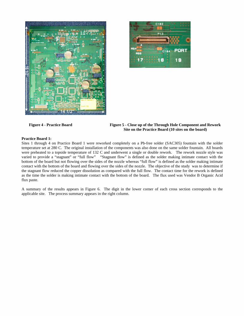
Figure 4 - Practice Board Figure 5 - Close up of the Through Hole Component and Rework Site on the Practice Board (10 sites on the board)
Practice Board 1: Sites 1 through 4 on Practice Board 1 were reworked completely on a Pb-free solder (SAC305) fountain with the solder temperature set at 280 C. The original installation of the components was also done on the same solder fountain. All boards were preheated to a topside temperature of 132 C and underwent a single or double rework. The rework nozzle style was varied to provide a “stagnant” or “full flow” “Stagnant flow” is defined as the solder making intimate contact with the bottom of the board but not flowing over the sides of the nozzle whereas “full flow” is defined as the solder making intimate contact with the bottom of the board and flowing over the sides of the nozzle. The objective of the study was to determine if the stagnant flow reduced the copper dissolution as compared with the full flow. The contact time for the rework is defined as the time the solder is making intimate contact with the bottom of the board. The flux used was Vendor B Organic Acid flux paste. A summary of the results appears in Figure 6. The digit in the lower corner of each cross section corresponds to the applicable site. The process summary appears in the right column.

Full View Topside View Bottomside View
Figure 6 - Cross Section and Process Summary for Sites 1, 2, 3, & 4 on Practice Board 1 (OSP) Measurements of copper thickness on Sites 1 through 4 were taken as shown in Figure 7. The Top Layer Pad Copper is on the topside of the board and the Bottom Layer Trace Copper is covered by masking. Both locations have negligible risk of copper dissolution and can be considered baselines for the original copper thickness. All measurements in Figure 7 are in mils.
Site 1 Single rework Stagnant Flow Contact Time for the original Installation = 11s Contact Time for the Single Rework = 21s Site 2 Single Rework Full Flow Contact time for the original installation = 9s
Contact Time for the Single Rework = 17s SITE 3 Double Rework Full Flow Contact Time for the Original Installation = 8s
Contact Time for the 1st Rework = 14s
Contact Time for the 2nd Rework = 15s
SITE 4 Double Rework Stagnant Flow
Contact Time for the Original Installation = 9 seconds
Contact Time for the 1st Rework = 15s
Contact Time for the 2nd Rework = 17s

LEAD FREE SOLDER FOUNTAIN REWORK - COPPER DISOLUTION
0.000
0.500
1.000
1.500
2.000
2.500
SITE 1SINGLE REWORKSTAGNANT FLOW
SITE 2SINGLE REWORK FULL
FLOW
SITE 3 DOUBLEREWORK FULL FLOW
SITE 4 DOUBLEREWORK STAGNANT
FLOW
REWORK SITE
CO
PPER
TH
ICK
NES
S (m
ils)
Top Layer Pad CopperBottom Layer Trace CopperBottom Pad CopperKnee Copper

Figure 7: Copper Thickness Measurements for Sites 1 – 4 on Practice Board 1 (OSP) Some observations from the data:
• All four sites were considered acceptable. There were no excessively thin or fractured knees, nor was there any significant via wall thinning near the surface. Copper thickness was above the IPC Class 3 minimum of .001” (1 mil).
• Copper dissolution increased for the double rework as compared with the single rework which was expected but the increase was smaller than anticipated.
• The difference in copper dissolution between the stagnant and full flow was not significant. • By the end of the double rework process, the bottom side pads have lost approximately one-quarter of their original
copper, regardless of method used. Practice Board 2 Practice Board 2 was used to assess a different rework process in which forced hot air convection was used to remove the connector and remove solder from the through holes. The solder fountain was only used to install the component. This process significantly reduced the contact time on the solder fountain which would likely further minimize copper dissolution. One connector location was subjected to a double rework and another connector was subjected to a triple rework and the two sites were referred to as 2X and 3X respectively. . The parameters for the hot air component removal and cleaning of the holes:
• Board topside preheat to 160 degrees C for component removal and cleaning of the holes • Component reflow temperature 225 degrees C – 240 degrees C
The parameters for the component installation on the solder fountain were as follows:
• Board Topside Preheat = 132 degrees C • Contact Time = 8 - 9 seconds
Copper thickness was measured and the data appears in Figure 8. The Top Layer Pad Copper is on the top of the board and the Bottom Pad Copper is covered by masking and have negligible risk of copper and can be considered baselines for the original copper thickness. All measurements in Figure 8 are in mils.

Figure 8 - Copper Thickness for the 2X and 3X Sites on Practice Board 2 (OSP): The measured results were acceptable for the 2X and 3X reworks per IPC Class 3 criteria. The copper thickness at the knees did not go below 1 mil and the amount of copper dissolution on the 2X and 3 X rework were equivalent which was somewhat surprising. Cross sections of the 2X and 3X rework appear below in Figure 9. The 2X or 3X figure in the lower part of the image denotes the respective rework.
2X / 3X REWORK
0
0.5
1
1.5
2
2.5
Top Layer Pad Copper Bottom Layer Trace Copper Bottom Pad Copper Knee Copper
FEATURE
CO
PPER
TH
ICK
NES
S (m
ils)
2X3X

Full View Top View Bottom View
Figure 9 - Cross Sections of the 2X and 3X Rework on Practice Board 2 (OSP) The cross sections of the 2X and 3X reworks were acceptable per IPC Class 3 criteria. The amount of copper dissolution was acceptable and the small amount of pad lifting is consistent with SnPb through hole reworks. The flow through of solder to the topside was 100%, there was minimal voiding, the wetting was good, and there was no thermal degradation of the laminate. Maverick Through Hole Rework: The Maverick Card is 84 mils thick, 16 layers with 7 ground/power planes. Compared to the Practice Boards, it represents a significantly more difficult rework challenge in terms of thermal load. The component selected for rework on the Maverick card was the 16 pin header at Location J6. The Maverick Card and the Header at Location J6 appear in Figures 10 and 11. Figure 10: Topside of the Maverick Card
.
Figure 11: Close up of the Through Hole Header reworked at Location J6. The arrow references
Location J6 on the board.

Maverick Card #3: OSP, Double Rework on the Solder Fountain: Based on the results from Practice Board 1 and 2 which indicated a double rework done on the solder fountain would be successful, it was decided to employ this process on Maverick Card #3 which had an OSP surface finish. This process is faster as compared with the alternative process which incorporates forced hot air for the component removal and hole clean. Maverick Solder Fountain Parameters for the Double Rework on Maverick Card # 3:
• Topside Board Preheat Temperature = 132 degrees C • Temperature of the Solder = 280 degrees C • Contact Time for Each Rework = 18 – 20 seconds • Total Contact Time for both Reworks = 36 – 40 seconds • Flux = Vendor B Flux Paste
The cross section results are seen in Figure 12:

PAD LIFTING HOLE WALL PULL-AWAY FRACTURED KNEES
Figure 12 - Cross Section of the 16 Pin Header on the Maverick Card #3 (OSP) after Double Rework on the Solder Fountain
The double rework was not acceptable per IPC Class 3 Criteria, and the fractured knees caused by copper dissolution is a known risk of Pb-free SAC305 rework and it has been documented previously. It should be noted the fractured knee could not be detected with visual inspection and required destructive cross sections for detection.
Maverick Card #4: Immersion Silver, Single Rework with Hot Air and Solder Fountain: Based on the unacceptable results for the double rework of the Maverick Card # 4 on the solder fountain, it was decided to perform a single rework incorporating the hot air platform for component removal and through hole cleaning. The solder fountain was only be used to install the component which significantly reduced the contact time on the solder fountain and minimized the risk of copper dissolution. However, the plastic body of the connector melted during the initial hot air removal. It was later determined that the plastic was only rated to 220 C (not compatible for Pb-free assembly) which made it more difficult to remove the component. The topside of the preheat of the board was increased to 180 C and the reflow temperature of the component was lowered to 220 – 230 and the component was removed from the board just before the plastic body completely melted. The component required 8 - 9 seconds of the contact on the solder fountain for installation. The cross sections are seen in Figure 13.
Maverick Card # 3 REWORK Here we see significant pad lifting on both sides of the board, as well as hole wall pull-away. The knees are fractured; one is seen in the bright field. image at the left. This process was not successful.

Figure 13 - Cross Section of the 16 Pin Header on the Maverick Card #4 (OSP) after Single Rework (Removal by Hot
Air and Installation by Solder Fountain) The single rework was successful in minimizing copper dissolution but induced some PCB thermal degradation. It was believed this was most likely caused by the high topside preheat (180 degrees C) combined with the extended time at this temperature required to reflow the component, remove the component, and vacuum the holes. The higher temperature was required to minimize the melting of the through-hole component and the profile would have been optimized if the through hole component was rated to a higher temperature. Based on the generally positive results with Maverick Card # 4, it was decided to conduct a double rework using the same technique on an OSP Maverick Card. The card selected was Maverick Card # 9 and the cross sections appear in Figures 14, 15, 16, and 17.
Maverick Card # 4 Cross Sections The single rework process was more benign to the board. As we see in these images, the knees remained intact and the copper is in generally much better shape than we saw with the double rework process. There was still some degree of pad lifting, as noted in the two images at the bottom. However, it varied from none at all to about 2 mils, across the section. Hole wall pull-away was less than 10% along the length of the via wall. This was a successful rework that produced acceptable results. With fine tuning, it may be possible to eliminate most of the observable pad lifting.

Figure 14 - Cross Section of the 16 Pin Header on the Maverick Card #9 (OSP) after Double Rework (Removal = Hot Air and Installation = Solder Fountain) Full View.

Figure 15 - Cross Section of the 16 Pin Header on the Maverick Card #9 (OSP) after Double Rework. Top View.

Figure 16 - Cross Section of the 16 Pin Header on the Maverick Card #9 (OSP) after Double Rework. Top View Showing Pad Lift.

Figure 17 - Cross Section of the 16 Pin Header on the Maverick Card #9 (OSP) after Double Rework. Bottom View Showing Copper Thickness at the Knee.
The technique significantly reduced copper dissolution as compared with the technique used for Maverick Card # 3. Flow through of solder to Side 1 was greater than 75%, wetting was good, and voiding was minimal. However, slight pad lifting was detected which may be related to the high board preheat temperature required for the low temperature rating of the through hole component being reworked. Moreover, this card was previously subjected to a double BGA rework prior to the double through hole rework and the increased number of thermal cycles may have also been a factor. The double rework technique used for Maverick Card # 9 was used for Maverick Card # 8 which is an ENIG board. The cross section is seen in Figure 18.

Figure 18 - Cross Section of the 16 Pin Header on the Maverick Card #8 (ENIG) after Double Rework. Full View. The joint in Figure 18 meets IPC Class 3 Criteria, but there is evidence of slight pad lifting which is not preferred. Copper dissolution was not an issue with ENIG surface finish.

BGA Rework on the Maverick Card: Double rework was conducted on a 304 Pin Pb-free Plastic BGA located at U29 on the topside or a 280 Pin Pb-free BGA located on the bottom side at U510. The rework was completed on each of the three board surface finishes and Vendor A was used for solder paste and liquid flux. Solder paste was micro stenciled on the site prior to installation of the BGA and flux paste was used to clean the site after the BGA was removed. A double rework on the same site is rare but a successful double rework may be necessary and it also provides a higher confidence level in the single rework. Maverick Card # 5: OSP Surface Finish, 304 Pin BGA The 304 Pin BGA at U29 was subjected to a double rework on the Maverick 5 (Mav5) card which means the original BGA was removed and replaced and the process was repeated after the board was allowed to cool to room temperature. The surface finish of the card was OSP, and Vendor A’s solder paste was used. The following are the applicable rework thermal parameters:
• Topside Board Preheat Temperature = 160 degrees C • Maximum Case (BGA Package) Temperature = 259 degrees C • Peak Joint Temperature = 245 and 243 degrees C • Time Above 217 degrees C for the Joints = 82 and 85 seconds
The card was tested electrically before and after the double rework and passed both tests. The cross sections in Figures 19 and 20 illustrate the results which are acceptable per IPC Class 3 criteria. There is good wetting, minimal voiding, good symmetry, and minimal copper dissolution on the pad. Moreover, no damage was observed to the PCB. However, the press pin connectors on the edge of the board were thermally degraded and had to be replaced after the double rework in order to complete the electrical testing. The press pin components were not rated to 260 C.
Figure 19 - Maverick Card #5 Double Rework on the Maverick Card OSP, 304 Pin BGA at U29.
Figure 20 - Close up of Figure 19.

A double rework was preformed in a similar fashion on the 304 Pin BGA on Maverick Card # 10 which had an ENIG surface finish. There was no evidence of thermal degradation and the BGA joints met IPC Class 3 criteria. A representative cross section appears in Figure 21.
Figure 21 - Maverick Card #10 Double Rework on the Maverick Card ENIG, 304 Pin BGA at U29.
A double rework was preformed in a similar fashion on the 280 Pin BGA on Maverick Card # 6 which had an ImAg surface finish. There was no evidence of thermal degradation and the BGA joints met IPC Class 3 criteria. A representative cross section appears in Figure 22.
Figure 22 - Maverick Card #6 Double Rework on the Maverick Card ImAg, 304 Pin BGA at U510.
Conclusions:
• The reliability of the Pb-free version of the Maverick card was deemed acceptable per the calculations made using the Coffin Manson Model.
• Overall, the Pb-free through-hole rework processes evaluated were successful. The solder fountain or a combination of the hot air platform and a solder fountain, are viable alternatives and the selection of the optimum rework process is predicated on the design and construction of the board.
• Additional optimization is required for the through hole rework process to minimize pad lifting. • Double rework of BGAs on an ENIG, ImAg, and OSP surface finish was acceptable and there was no evidence of
thermal degradation to the PCB or BGA.

• All components should be rated for the higher temperatures associated with Pb-free assembly and rework. The through-hole header reworked on the Maverick Card was only rated to 220 C and melted during hot air removal. Similarly, the press fit connectors, which were exposed to the bottom heaters during through-hole and BGA rework, exhibited thermal degradation.
Acknowledgements: The authors would like to thank Gene Bridgers of Mercury Computer Systems, George Blais Jr, David Cavanaugh, Dorothy Martin, Eduart Pengu, Rosemarie St. Laurent, Beatrice Sybert, and Bruce Tostevin and Robert Finch of Benchmark Electronics for their assistance performing the rework, analyzing the boards, and contributing to this paper.

1
Transition to Lead-free Electronics Assembly: Case Study Part II
Authors: Robert Farrell & Scott Mazur & Paul Bodmer
Benchmark Electronics
Gregory MoroseMassachusetts Toxics Use Reduction Institute
Gene Bridgers & Richard RussoMercury Computer Systems, Inc.
IPC / JEDEC - Global Lead Free Conference April 11, 2007
Boston, MA

2
Lead-free Assembly:Maverick Board
Good mix of double-sided SMT and THT components.The PCB dimensions are 7.5” X 9.2” and 84 Mils thick.

3
Key LessonsCreate a proper baseline of tin/lead process performance and quality metrics. This will be critical to compare the process and quality results for the new lead-free electronics assembly process.
Determine availability of lead-free compatible components because the supply chain is not completely ready. The components should have a lead-free finish and the ability to withstand the higher temperature profile associated with lead-free electronics assembly.
The mean defect level for the lead-free assembly process was not influenced by the three board surface finishes (OSP, Imm Ag, ENIG) chosen or the two stencil designs used for this case study.
Further, it can be stated with 95% confidence that there is no difference between the median defects per board or variance between the tin/lead and lead-free process. These conclusions are consistent for the analysis of the total defects, as well as the analysis of the solder-related defects only.

4
Thermal Cycling ParametersSix boards (2 OSP, 2 ImAg, 2 ENIG) were subjected to the following thermal cycling parameters:
• -40 degrees C to 85 degrees C temperature extremes• Minimum 30 minute dwell at each extreme• Maximum slope of 20 degrees C/minute• No Vibration• 500 cycles• Cards were electrically tested prior to the start of
thermal cycling and after each 100th cycle

5
Thermal Cycling Results
• Five boards successfully completed 500 cycles and one board failed between the 400th and 500th cycle.
• The applicable data for 400 thermal cycles was entered into the Coffin Manson model using the SnPb constant and exponents.
• The justification is that SnPb and SAC305 are both soft metal systems and most studies to date have established comparability in reliability performance between these two alloys in most applications.

6
Thermal Cycling Conclusions
• Assuming the "Normal Use" application is one power cycle per day, the Coffin-Manson relationship allows an estimate of the equivalent use.
• Based on six boards with no failures before the 400th cycle, the equivalent use during the 400 cycles would be 3,632 years.

7
Thermal Cycling Conclusions (cont)
Assuming significant reductions in the estimate of the equivalent use due to the uncertainty of the Coffin Manson equation for Pb-free, the end customers were confident the reliability of the Pb-free version of this product would be equal to or better than the SnPb version.
Data indicated there was no difference among the three Printed Circuit Board (PCB) surface finishes.

8
Failure Analysis
• Card that failed thermal cycling between the 400th and 500th cycle was an OSP card.It was subjected to failure analysis and two modes of failure were determined on separate BGAs:
a) Broken PCB Etch at corner of the BGAb) Sphere to BGA package failure

9
Broken Etch at Corner of Ceramic BGA (post thermal cycling)

10
Practice Board for Through HoleProcess Development Work
• 16.5” by 14.5”• OSP Surface Finish• 74 Mils Thick• 10 Layers

11
Practice Board #1
Solder Fountain Rework:
-SAC305 at 280 C-Topside Board Preheat to 150 C-Stagnant and Full Flow on the Nozzle-Single and Double Rework

12
Practice Board #1 Results(Copper Dissolution)
LEAD FREE SOLDER FOUNTAIN REWORK - COPPER DISOLUTION
0.000
0.500
1.000
1.500
2.000
2.500
SITE 1SINGLE REWORKSTAGNANT FLOW
SITE 2SINGLE REWORK FULL
FLOW
SITE 3 DOUBLEREWORK FULL FLOW
SITE 4 DOUBLEREWORK STAGNANT
FLOW
REWORK SITE
CO
PPER
TH
ICK
NES
S (m
ils)
Top Layer Pad CopperBottom Layer Trace CopperBottom Pad CopperKnee Copper

13
Practice Board # 2
• Forced Convection Platform Used for Component Removal and Cleaning of Through Holes
• Solder Fountain used to Install Components. Same Parameters as Practice Board # 1
• Double (2x) and Triple (3x) Rework

14
Practice Board 2 ResultsCopper Dissolution
2X / 3X REWORK
0
0.5
1
1.5
2
2.5
Top Layer Pad Copper Bottom Layer Trace Copper Bottom Pad Copper Knee Copper
FEATURE
CO
PPER
TH
ICK
NES
S (m
ils)
2X3X

15
Through Hole Rework on the Maverick Card
.
:Close up of the Through Hole Header reworked at Location J6. The arrow references Location J6 on the board.

16
Double Rework on Maverick Card # 3, OSP
• Solder Fountain Used for All Rework– SAC305 at 280 Degrees C– Topside Board Preheat to 150 Degrees C
Step Contact Time (seconds)Installation 91st Rework 202nd Rework 20
Total = 49 seconds

17
Results for the Maverick OSP Card # 3 Double Rework (Unacceptable)
Top view of the Through Hole JointBottom view showing copper
dissolution at the knee

18
Double Rework on Maverick Card #9, OSP
• Forced Convection Used to Remove Component and Clean Holes
• Solder Fountain Used to Install Component/Same Parameters as Card # 3Step Contact Time (seconds)Installation 9 1st Rework 92nd Rework 9
Total = 27 seconds

19
Results for the Double Rework on Maverick Card #9, OSP
(Acceptable Copper Thickness)
Bottom view of through hole joint

20
Maverick BGA Rework
• Double Rework• 280 or 304 Pin Plastic BGA’s• OSP, ImAg, and ENIG Surface Finishes• Acceptable Results Obtained on all 3
Surface Finishes

21
Representative Results after Double BGA Rework on an OSP
Maverick CardPackage
Board

22
Conclusions
• The reliability of the Pb-free version of the Maverick card was deemed acceptable per the calculations made using the Coffin Manson Model.
• Overall, the Pb-free through-hole rework processes evaluated were successful.
• The solder fountain or a combination of the hot air platform and a solder fountain, are viable alternatives and the selection of the optimum rework process is predicated on the design and construction of the board.

23
Conclusions (cont)
• Additional optimization is required for the through hole rework process to minimize pad lifting.
• Double rework of BGAs on an ENIG, ImAg, and OSP surface finish was acceptable and there was no evidence of thermal degradation to the PCB or BGA.

24
Conclusions (cont)
• All components should be rated for the higher temperatures associated with Pb-free assembly and rework. – Through-hole header reworked on the
Maverick Card was only rated to 220 C and melted during hot air removal.
– Press fit connectors, which were exposed to the bottom heaters during through-hole and BGA rework, exhibited thermal degradation.