transistor technology evokes new physicstransistor technology evokes new physics nobel lecture,...
TRANSCRIPT

WI L L I A M SH O C K L E Y
Transistor technology evokes new physics
Nobel Lecture, December 11, 1956
Introduction
The objective of producing useful devices has strongly influenced the choiceof the research projects with which I have been associated. It is frequentlysaid that having a more-or-less specific practical goal in mind will degradethe quality of research. I do not believe that this is necessarily the case andto make my point in this lecture I have chosen my examples of the newphysics of semiconductors from research projects which were very definitelymotivated by practical considerations.
An important fraction of United States industry adheres to the idea thatresearch of a fundamental character is worthwhile from a practical point ofview. This is outstandingly the case at Bell Telephone Laboratories wheremy co-prizewinners and I, together with our many colleagues, carried outthe work described in these lectures. The attitude of Bell Telephone Labor-atories has undoubtedly resulted to a substantial degree from the viewpointsof the four men who have been its research directors and subsequently itspresidents. Each of these men, H. D. Arnold, F. B. Jewett, O. E. Buckley,and M. J. Kelly, has also been active and effective in governmental or civicaffairs. All had obtained a thorough indoctrination in the research view-point in the course of their doctorate training in physics. My personal contactwith two of these men had a significant influence on my planning of semi-conductor research programs as I shall mention below.
My decision to come to Bell Telephone Laboratories immediately afterobtaining my Ph.D. in 1936 was strongly influenced by the fact that mysupervisor would be C. J. Davisson. Upon my arrival I was assigned byDr. M. J. Kelly to an indoctrination program in vacuum tubes. In the courseof this program Dr. Kelly spoke to me of his ideal of doing all telephoneswitching electronically instead of with metal contacts. Although I did notchoose to continue work on vacuum tubes and was given freedom to pursuebasic research problems in solid-state physics, Dr. Kelly’s discussion left mecontinually alert for possible applications of solid-state effects in telephone

T R A N S I S T O R T E C H N O L O G Y E V O K E S N E W P H Y S I C S 345
switching problems. Insofar as my contribution to transistor electronics hashastened the day of a fully electronic telephone exchange, it was stronglystimulated by the experiences given me during my early years at the Labor-atories.
Before leaving the subject of research in industry, I would like to expresssome viewpoints about words often used to classify types of research in phys-ics; for example, pure, applied, unrestricted, fundamental, basic, academic,industrial, practical, etc. It seems to me that all too frequently some of thesewords are used in a derogatory sense, on the one hand to belittle the practicalobjectives of producing something useful and, on the other hand, to brushoff the possible long-range value of explorations into new areas where auseful outcome cannot be foreseen. Frequently, I have been asked if an exper-iment I have planned is pure or applied research; to me it is more importantto know if the experiment will yield new and probably enduring know-ledge about nature. If it is likely to yield such knowledge, it is, in my opinion,good fundamental research; and this is much more important than whetherthe motivation is purely esthetic satisfaction on the part of the experimenteron the one hand or the improvement of the stability of a high-power tran-sistor on the other. It will take both types to « confer the greatest benefit onmankind » sought for in Nobel’s will.
The five basic imperfections
Before discussing the selected group of experiments in transistor physics, Ishall extend somewhat farther Dr. Bardeen’s remarks1 about the characteris-tics and interactions of electrons, holes, donors and acceptors. For this pur-pose I shall use a reference to water solutions of acids, bases and salts as anaid to exposition.
The dissociation of pure water to positive hydrogen ions and negativehydroxyl ions satisfies the mass-action law
[H+] [OH-] = function of T
where the concentration of H2O is so nearly constant for dilute solutionsthat it may be taken as constant and not shown explicitly. This equationhas as its analogue

346 1 9 5 6 W . S H O C K L E Y
=
for a semiconductor where n and p are the electron and hole concentrations.The equation is accurate, provided neither n nor p is so large that its statisticsbecome degenerate. The normal electron-pair bond here plays the role of anundissociated water molecule. In pure deionized water and in a pure semi-conductor, electrical neutrality requires that the concentration of the positivecharges equals that of the negative charges:
[H+] = [OH-] and p = n
A semiconductor which is so pure that impurities do not affect the propertybeing considered is called intrinsic in regard to such a property. Using thesubscript i to designate this case, we have
p i = n i a n d ni2 = f ( T )
The concentration ni is referred to as the intrinsic concentration.The chemical analogue to an n-type semiconductor is a base and the
charge neutrality equations are
[H+] + [Na+] = [OH-]
p + Nd = n
where Nd is the concentration of donors and it is assumed that all donors arefully ionized.
Similarly a p-type semiconductor is analogous to an acid:
[H+] = [OH-] + [Cl-]
p = n + Na ,
where Na is the acceptor concentration.A neutral salt also has its analogue which is called a compensated semicon-
ductor. For this case the donor and acceptor concentrations are equal so thatthe equation for electrical neutrality
p + Nd = n + Na

T R A N S I S T O R T E C H N O L O G Y E V O K E S N E W P H Y S I C S 347
reduces to equality of n and p so that each is equal to ni. The electrical con-ductivity of a perfectly compensated silicon or germanium crystal is almostequal to that of an intrinsic crystal; there may be a small difference due tothe reduction of mobility by scattering by the charged ions. The differencebetween the low conductivity of the perfectly compensated semiconductorand the high conductivity of a neutral salt solution arises from the fact thatthe donors and acceptors are tied in place in a semiconductor while the cat-ions and anions of a salt have mobilities comparable to that of an OH-ion.
Compensation, or rather overcompensation, plays a vital role in the man-ufacture of semiconductor devices. For example, it permits the conversionof n-type material to p-type by the addition of acceptors without the priorremoval of donors. A crystal grown from an n-type melt may be changedto p-type by adding an excess of acceptors.
The words majority and minority are frequently useful in discussing semi-conductors. In an n-type specimen, the majority carriers are electrons andthe minority carriers are holes.
Holes, electrons, donors and acceptors represent four of the five classes ofimperfections that must be considered in semiconductor crystals in order tounderstand semiconductor effects. The fifth imperfection has been given thename deathnium. The chemical analogue of deathnium is a catalyst. In thecase of water as the analogue to a crystal, there is, so far as I know, noimportant corresponding catalyst. What deathnium does is to hasten theestablishment of equilibrium between holes and electrons. If, due to the vari-ous possible disturbances important in transistor electronics, the concentra-tion of minority carriers is, for example, substantially raised, then the minor-ity carriers will combine with the majority carriers to produce normal elec-tron-pair bonds, by this means restoring equilibrium. Deathnium catalyzesthis recombination process. The symbols for the five imperfections areshown in Table 1.
Table I.
1. - (excess) electron2. + hole3 deathnium4. ⊕ donor5. acceptor
The role of deathnium can be illustrated in terms of the phenomenon ofphotoconductivity. If light shines on a germanium crystal, then the pairs of

348 1 9 5 6 W . S H O C K L E Y
electrons and holes that are formed will impart a conductivity to the crystal.This conductivity is known as photoconductivity. If the source of light isremoved, the photoconductivity will die away, due to the recombinationof the holes and the electrons. Thus, if an electron falls into an incompletebond, one hole-electron pair will be eliminated.
The photoconductivity dies away with a characteristic time known as thelifetime. Thus, after the light is turned off, the photoconductivity will dropto approximately one-half its value in one lifetime. This process continueswith a reduction of approximately one-half in each subsequent period ofone lifetime.
If the process of recombination of holes and electrons were a direct one,the lifetime would be the same in all germanium crystals. It is found exper-imentally, however, that two otherwise very similar germanium crystals willhave lifetimes that differ by as much as 1,000 fold. In one crystal, the life-time may be a millisecond, whereas in another it may be a microsecond.This variation in lifetime requires the presence of some sort of imperfectionwhich catalyzes the recombination of the holes and the electrons.
Actually, there are several forms of deathnium. For example, if electronshaving an energy of several million electron volts fall upon a germaniumcrystal, the lifetime is subsequently reduced2. From the investigation at Pur-due University, it is known that such bombardment produces disorder ofthe germanium atoms3. A high-energy electron can eject a germanium atombodily from its normal position in the crystal structure, thus leaving a va-cancy behind, where there should be an atom, and causing the ejected atomto become either an extra atom or an interstitial atom fitting into a place inthe structure which would normally be empty. It has been found at BellTelephone Laboratories that these disordering effects function as deathnium.It has also been found that copper and nickel chemical impurities in thegermanium produce marked reductions in lifetime4.
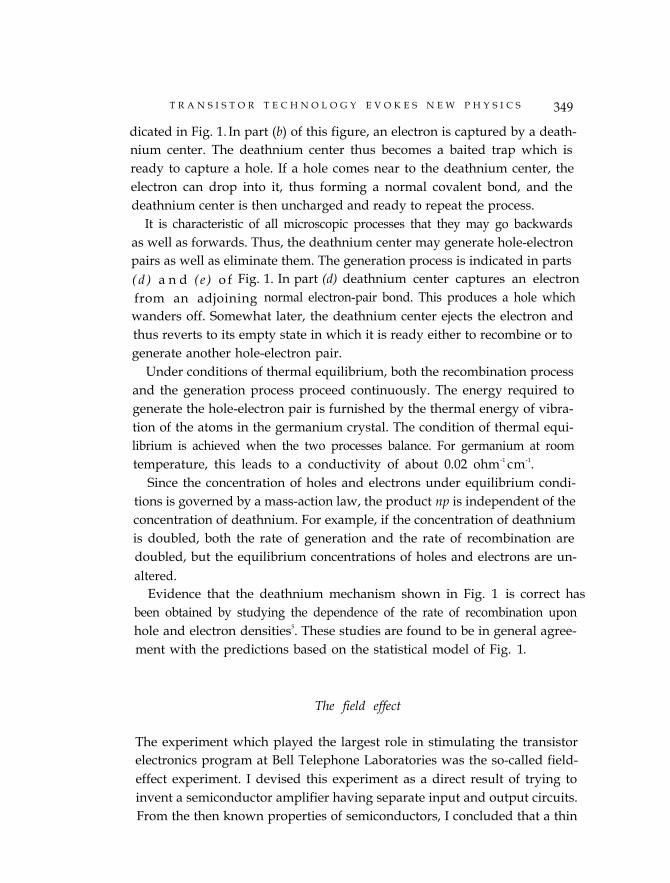
The way in which deathnium catalyzes the recombination process is in-
Fig. 1. A recombination center (deathnium) captures alternately an electron and a holeand thus catalyzes their recombination, as shown in parts (a), (b), and (c). The thermal-
ly activated generation process is shown in (d) and (e).
T R A N S I S T O R T E C H N O L O G Y E V O K E S N E W P H Y S I C S 349
dicated in Fig. 1. In part (b) of this figure, an electron is captured by a death-nium center. The deathnium center thus becomes a baited trap which isready to capture a hole. If a hole comes near to the deathnium center, theelectron can drop into it, thus forming a normal covalent bond, and thedeathnium center is then uncharged and ready to repeat the process.
It is characteristic of all microscopic processes that they may go backwardsas well as forwards. Thus, the deathnium center may generate hole-electronpairs as well as eliminate them. The generation process is indicated in parts( d ) a n d ( e ) o f Fig. 1. In part (d) deathnium center captures an electronfrom an adjoining normal electron-pair bond. This produces a hole whichwanders off. Somewhat later, the deathnium center ejects the electron andthus reverts to its empty state in which it is ready either to recombine or togenerate another hole-electron pair.
Under conditions of thermal equilibrium, both the recombination processand the generation process proceed continuously. The energy required togenerate the hole-electron pair is furnished by the thermal energy of vibra-tion of the atoms in the germanium crystal. The condition of thermal equi-librium is achieved when the two processes balance. For germanium at roomtemperature, this leads to a conductivity of about 0.02 ohm-1 cm-1.
Since the concentration of holes and electrons under equilibrium condi-tions is governed by a mass-action law, the product np is independent of theconcentration of deathnium. For example, if the concentration of deathniumis doubled, both the rate of generation and the rate of recombination aredoubled, but the equilibrium concentrations of holes and electrons are un-altered.
Evidence that the deathnium mechanism shown in Fig. 1 is correct hasbeen obtained by studying the dependence of the rate of recombination uponhole and electron densities5. These studies are found to be in general agree-ment with the predictions based on the statistical model of Fig. 1.
The field effect
The experiment which played the largest role in stimulating the transistorelectronics program at Bell Telephone Laboratories was the so-called field-effect experiment. I devised this experiment as a direct result of trying toinvent a semiconductor amplifier having separate input and output circuits.From the then known properties of semiconductors, I concluded that a thin

350 1 9 5 6 W. S H O C K L E Y
film of silicon or germanium would have a substantial change in its con-ductivity if it were made into one of a pair of condenser plates and the con-denser strongly charged. The surface charge, if represented as a change inmobile carriers, could appreciably increase or decrease the conductance ofthe film.
A number of experiments were initially tried using evaporated layers andother thin layers. These all gave negligible effects and progress was at astandstill until Bardeen proposed his theory of surface states to explain thelack of an observable effect.
Bardeen’s model also explained a number of other previously mysteriousphenomena6 and led to the suggestion of doing the field-effect experimentat liquid-air temperature to immobilize the surface states. This gave the firstpositive result. How this led to a sequence of experiments culminating inthe point-contact transistor is discussed in Dr. Bardeen’s lecture1. The firstpublication of a positive effect was made by G. L. Pearson and the writerin 19487.
At the present time the field-effect experiment is playing a very importantrole in measuring the properties of semiconductor surfaces8.
On the practical side the field-effect has been utilized to make transistoramplifiers having interesting properties quite different from those of junc-tion transistors.
Injection and drift
At the time of the discovery of the point-contact transistor by Bardeen andBrattain there were a number of unresolved questions regarding its modeof operation. The original transistor showed evidence that the coupling be-tween the input or emitter point and the output or collector point took placethrough conduction in a thin surface layer of conductivity type opposite tothe underlying or base material. Somewhat later the idea that the emitterpoint might actually be injecting minority carriers into the body of thesemiconductor developed. The development of this idea came as a result oftwo independent events: the invention of the junction-transistor structureby the present writer (as discussed below, injection plays an essential role inthe junction transistor) and the observation by J. N. Shive9 that transistoraction could occur with the points on opposite sides of a thin slab of semi-conductor.

In order to test the model of carrier injection, J. R. Haynes and the authorcollaborated in the drift-mobility experiment or « Haynes’ experiment » ongermanium specimens 1 0. In order to understand the significance of the ex-periment in elucidating transistor action the mechanism of current flow atthe metal-semiconductor contact must be considered.
In Fig. 2, the metal is represented in a highly pictorial fashion. The valenceelectrons in a metal are thought of as forming an electron gas, which per-meates the entire structure. Thus, the electrons are not held in position invalence bonds as they are in an insulator. The electron gas can flow freelythrough the structure of the metal, and this fact accounts for the high con-ductivity of metals. In the upper part of Fig. 2 one of the processes for re-moving electrons from the semiconductor is represented. Since the semi-conductor is n-type, it contains excess electrons; these excess electrons maybe drawn to the metal by its positive charge and thus enter the metal toproduce a current of electrons flowing out of the emitter point through theconnecting lead.
Another possible mechanism for electron transfer from semiconductor tometal is shown in the lower part of Fig. 2. In this case, an electron is with-drawn from one of the valence bonds adjacent to the metal. This process
352 1 9 5 6 W . S H O C K L E Y
also transfers an electron from the semiconductor to the metal, but whenthe transfer occurs, a hole is left behind. The hole is repelled by the positivecharge on the emitter contact and moves deeper into the semiconductor.
Both of the processes discussed above have the same effect so far as themetal emitter point and conducting leads to the emitter point are concerned.Both produce a net flow of electrons from semiconductor to the emitterpoint and through the leads to the emitter terminal. It is thus evident thatsome more subtle experiment than simply measuring the current to theemitter point is necessary to show that both processes of electron removalfrom the semiconductor occur. Suitable experiments have been planned andperformed, with the result that it is possible to show that both of the pro-cesses of Fig. 2 occur and also to determine the fraction of current carriedby each. In fact, in a good emitter point it can be shown that more than90 per cent of the current is carried by the process which injects holes intothe semiconductor, and less than 10 per cent by the process which removeselectrons.
In an ideal emitter point, all of the current would be carried by the hole-injection process. The reason for this result is that the electron-removal pro-cess does not disturb the state of affairs within the semiconductor. If electronsare removed from the semiconductor in the neighborhood of the emitterpoint, they are promptly replaced by electrons flowing from more distantparts of the semiconductor, and these electrons in turn are replaced by otherelectrons flowing in from whatever contact to the semiconductor completesthe electrical-current path or circuit. In the hole-injection process the situa-tion is quite different. Normally, the number of holes in the n-type semi-conductor is negligible so far as a contribution to the conductivity is con-cerned. However, when electrons are removed from the valence bonds andholes are injected, relatively large numbers of holes will be introduced. Theconductivity of the semiconductor will be increased in the neighborhoodof the emitter point in much the same fashion that it would be if light wereto shine on the semiconductor and produce hole-electron pairs. This disturb-ance in the electronic structure can be used to produce amplifying action inthe transistor.
Instead of discussing the quantitative experiment which is used to distin-guish between the two processes shown in Fig. 2, I shall describe a qualita-tive experiment which shows that hole injection does occur at an emitter point.This experiment permits quantitative studies to be made of the behavior ofholes and provides a method for the direct measurement of diffusion and drift.

T R A N S I S T O R T E C H N O L O G Y E V O K E S N E W P H Y S I C S 353
Fig. 3. Schematic representation of experiment to observe the drift and diffusion ofinjected holes in n-type germanium.
The experimental arrangement, which was first carried out in this formby J. R. Haynes, is illustrated diagrammatically in Fig. 3. The germaniumspecimen is in the form of an elongated point-contact transistor. There is,however, an extra contact on the base. The germanium is present as a rod,about 1/32 of an inch in cross section and approximately 1 inch long. A« sweeping field » is applied from end to end of the rod by a battery. This fieldacts in such a direction as to draw electrons from right to left through therod. If any holes were introduced in the rod, they would drift from left toright.
When the pulse generator at the left-hand point contact, or emitter point,operates, the emitter point is biased positive and thus in the forward direc-tion. According to the ideas presented in Fig. 2, this condition causes holesto be injected into the rod. These holes are then drawn down the rod bythe sweeping field. After a time they arrive in the neighborhood of the col-lector point, which, as the figure shows, is biased negative. It thus tends toattract holes, and some of the holes flow to the collector point and thus con-tribute to the current flowing in the collector circuit. This current flowsthrough a resistor, and the voltage across the resistor is applied to the verticalplates of a cathode-ray oscilloscope.
Under operating conditions, the operation of the pulse generator is ac-complished electronically and is synchronized with the functioning of theoscilloscope, so that just before the switch is closed, the electron beam inthe oscilloscope starts to move across the tube face from left to right. Attime t1 the switch to the emitter point is closed for a brief moment; the timeof closing is indicated by a « pick up » signal on the face of the oscilloscope.After this nothing happens until time t2 when some of the holes arrive atthe collector point; the concentration of holes builds up for a moment and

354 1 9 5 6 W . S H O C K L E Y
then decays as the group of holes injected at time t2 passes by the collectorpoint. The arrival pulse at the collector point is not so sharp as the « pick up »pulse because the holes, which were injected approximately at one pointand at the same time, spread out by diffusion so that by the time the groupof holes reaches the collector point it is relatively large in extent along therod.
It is evident that this experiment permits observation and measurement ofboth diffusion and drift. It is possible to measure the distance between thepoints and the electric field between the points; by calibrating the oscillo-scope, the time of travel may be measured. Thus the drift velocity may bemeasured directly, verifying the fact that the disturbance occurring at theemitter point behaves precisely as would be expected if the emitter pointinjected small numbers of positive carriers into the rod. For example, if thedistance between the points is doubled, the time lag between pick-up at t1
and the arrival of the pulse is also doubled. This result shows that the carriersdrift at a constant drift speed in the rod. But if the sweeping field is doubled,the time lag is cut in half. This fact shows that the speed of the carriers isproportional to the electric field. If the polarity of the sweeping field is re-versed, we would expect the injected carriers to be drawn to the left in thefilament so that none arrive at the collector point, and it is found exper-imentally that this is true.
As was indicated above, the spread of the time of arrival of holes is ameasure of the diffusion constant. From studies of the dependence of thisspread upon the transit time from emitter to collector, it can be verified thatthe holes spread out in accordance with the laws expected for diffusionphenomena. The value of the diffusion constant D can also be measured.
J. R. Haynes and his colleagues have performed various experiments ofthis sort. They have also experimented with the case of electron injectioninto p-type germanium and have dealt with the two corresponding casesfor silicon. The values of mobility and diffusion constant which they obtainin this way11 are tabulated in Table 2.

T R A N S I S T O R T E C H N O L O G Y E V O K E S N E W P H Y S I C S 355
It should be noted from Table 2 that in each case the ratio of diffusionconstant to mobility is approximately 1/40, and the dimensions of this quan-tity are in volts. In other words, the ratio of D to µ is 25 millivolts. This valuehas a fundamental significance, and the relationship between D and µ is com-monly known as the Einstein relationship. This relationship has recently beeninvestigated in detail, by the means described above, for germanium12. Thesignificance of this value of 25 millivolts is that an electron moving withrandom thermal energy will, on the average, be just capable of surmountinga potential hill of 25 millivolts. In other words, 25 millivolts is the electro-static potential corresponding to thermal energy for one electron. Put in an-other way, it can be stated that if any electron was set in motion with thermalenergy in free space against any electric field, the electron would be sloweddown by the electric field and by the time it had moved 25 millivolts againstthe field its velocity would be brought to zero and it would start to movein the opposite direction. The fact that a value of 25 millivolts is obtainedshows that the charge of the carriers which are drifting and diffusing inthe Haynes experiment is the electronic charge. If it were half or twice thisvalue, for example, the ratio of D to µ would be 50 or 12.5 millivolts, res-pectively.
When the Haynes experiment was first carried out, the procedure wasvaried by placing the two points on opposite sides of the filament and byusing filaments of much greater width than thickness. All these experimentsindicated that the interaction between the points took place through the bulkrather than over the surface.
Hot electrons and Ohm’s law
Another fundamental experiment on the behavior of electrons and holes insemiconductors had its origin in a practical aim. Sometime during 1948 inan attempt to see how semiconductors could be made to amplify at veryhigh frequencies, I came upon an idea which was independently discoveredand first published as the Staueffekt by H. A. Krömer13. Krömer does notappear to have considered the effect from the point of view of amplification,and its utilization for this purpose was first published in 1954 14.
The basic principle of the staueffect may be understood as follows : a holein the valence band will lose energy to phonons at a maximum rate P (max)
356 1 9 5 6 W . S H O C K L E Y
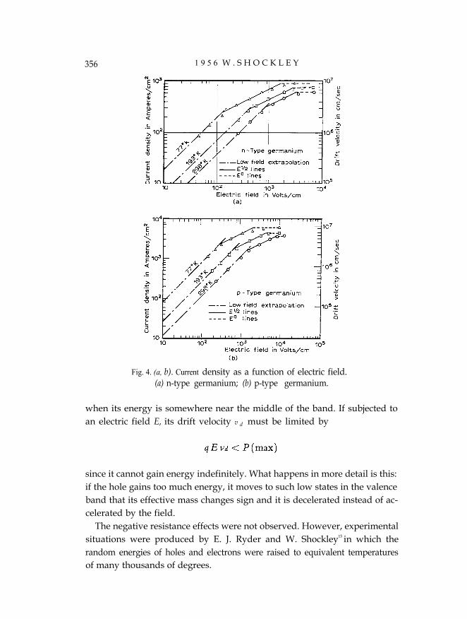
Fig. 4. (a, b). Current density as a function of electric field.(a) n-type germanium; (b) p-type germanium.
when its energy is somewhere near the middle of the band. If subjected toan electric field E, its drift velocity v d must be limited by
since it cannot gain energy indefinitely. What happens in more detail is this:if the hole gains too much energy, it moves to such low states in the valenceband that its effective mass changes sign and it is decelerated instead of ac-celerated by the field.
The negative resistance effects were not observed. However, experimentalsituations were produced by E. J. Ryder and W. Shockley15 in which therandom energies of holes and electrons were raised to equivalent temperaturesof many thousands of degrees.

T R A N S I S T O R T E C H N O L O G Y E V O K E S N E W P H Y S I C S 357
Fig. 4. (c, d). Current density as a function of electric field.(c) n-type silicon; (d) p-type silicon.
These effects represent a fundamental deviation from Ohm’s law in thesense that they result solely from the magnitude of the electric field and notfrom side effects such as changing numbers of holes and electrons due tochanging temperature.
Fig. 4 shows several curves representing how the drift velocity of holesand electrons varies with electric field as reported by Ryder16. Although thegeneral features of the curves are well understood, they are not yet ad-equately explained quantitatively1 7. The discrepancy between simple theoryand experiment probably results from the complex structure of the energysurfaces for holes and electrons, that is, from deviations from the single-effective-mass model of semiconductors.
From a practical point of view, non-linearities in the drift velocity areimportant in calculating the characteristics of semiconductor devices.
358 1 9 5 6 W. S H O C K L E Y
The p-n junction and single crystals
The rectifying contacts of chief importance in the early days of transistorphysics were made by pressing pointed wires on the semiconductor and sub-sequently conditioning them (« forming ») by passing heavy current. It wasdifficult at the time to interpret these procedures from an atomic point ofview and this is still true at present.
An important decision in the year following the invention of the transistorwas to place emphasis upon p-n junctions in the interior of the semicon-ductor rather than upon point contacts. From earlier work it was knownthat such junctions were rectifying and photosensitive. However, their char-acteristics were not entirely understood in terms of atomic models. Since ap-n junction can occur in a single crystal simply by a change in impuritycontent from donor dominated in the n-region to acceptor dominated inthe p-region, it is a far simpler structure than a metal semiconductor contactand its behavior highly predictable on theoretical grounds. It seemed logical,therefore, to attempt to understand p-n junctions first and point contactslater.
Another reason for choosing to emphasize p-n junctions was the possi-bility of producing junction transistors, a possibility published in 194918.
A p-n junction is the simplest so-called compositional structure in semicon-ductor electronics. By a compositional structure is meant a single crystal ofsemiconductor in which the composition in terms of the donor and acceptorcontent varies in a systematic and controlled way. Before describing the the-ory of the functioning of a p-n junction, I would like to say something aboutthe way in which p-n junctions whose behavior was satisfactory from atheoretical point of view were first achieved at Bell Telephone Laboratories.This history also is an example of the interaction of practical needs on aresearch program.
To begin, with attempts were made, particularly by M. Sparks, to pro-duce p-n junctions by allowing molten drops of germanium of one con-ductivity type to fall upon a heated block of germanium of the other con-ductivity type. Although p-n junctions were obtained by these means, theircharacteristics failed to live up to the predictions of theory. (The problemswere almost certainly those of cleanliness - the importance of copper wasnot known at the time.)
As a result of the needs of the Development Department for uniform ma-terial for the purpose of making experimental transistors, a program was

T R A N S I S T O R T E C H N O L O G Y E V O K E S N E W P H Y S I C S 359
Fig. 5. A p-n junction and the distribution of imperfections in it. (For simplicity,compensating pairs of donors and acceptors are not shown.)
set up to grow large single crystals of germanium. It is interesting to notethat the actual decision and emphasis on this program was due principallyto J. A. Morton, who headed the transistor-development group, rather thanby my own group or other research groups. I felt at the time that scientificstudies could adequately be carried out by cutting small specimens frompolycrystalline masses of material. As a result of Morton’s urging, G. K.Teal, with the collaboration of J. B. Little, made an experimental apparatusfor « pulling » single crystals of germanium from a melt of germanium heatedin a graphite crucible into which was dipped a small single-crystal seed19.The recent advances of transistor science and technology are founded onthese crystals. The addition of acceptors to an n-type melt during pullingchanged the solidifying material from n- to p-type and gave the first goodp-n junctions.
Another extremely important development in the preparation of mate-rials should be mentioned. This is the method of zone refining invented byW. G. Pfann, also of Bell Telephone Laboratories20. Noting that impuritiestend to be more soluble in molten germanium than in solid germanium.
360 1 9 5 6 W . S H O C K L E Y
Pfann devised a system of repetitive purification by crystallization. By mak-ing an elongated graphite boat and providing means to heat locally a smalllength or zone of it, he was able to pass molten zones successively fromone end to the other of the germanium and by this means to sweep im-purities clear of the major portion of the crystal and to concentrate themnear one end. By this means germanium crystals having one impurity atomin about 1010 germanium atoms have been produced. The density of im-purities in these crystals is thus comparable to the density of molecules in agas at a pressure of 10-5 millimeters of mercury. It is appropriate to call zonerefining the vacuum pump of transistor electronics.
Fig. 5 represents a p-n junction. In discussing its electrical properties, wewill be concerned with the five kinds of imperfections shown in the lowerpart of the figure. From a mechanical point of view the crystal is practicallyhomogeneous and perfect. A typical concentration for impurities in the crys-tal might be 1015 cm-3. This density of imperfections is so low that if onewere to traverse a row of atoms from end to end in the crystal one would,on the average, strike only about ten imperfections. Thus the crystal struc-ture itself is only slightly altered by the presence of the imperfections. Fromthe electrical point of view, on the other hand, the imperfections have pro-found effects.
As is shown in Fig. 5, the electrons are found chiefly in the n-region wherethey neutralize the chemical space charge of the donors, and the holes aresimilarly found in the p-region. In order for this situation to persist, as itdoes under conditions of thermal equilibrium, there must be an electric fieldpresent in the crystal. The idea that an electrical field is present in a conductorunder conditions of thermal equilibrium is at first surprising. However, thenecessity for such an electric field can readily be seen in terms of Fig. 5.Let us first of all suppose that no electric field is present across the junction;then as a result of diffusion, holes will cross the junction from left to rightand electrons will similarly diffuse across the junction from right to left. Asa result, there will be a net transfer to the right of positive charge acrossthe junction. This will result in an electric field which will build up to justsuch a point that further current flow is prevented.
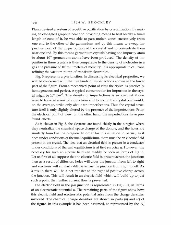
The electric field in the p-n junction is represented in Fig. 6 (a) in termsof an electrostatic potential ψ. The remaining parts of the figure show howthis electric field and electrostatic potential arise from the charge densitiesinvolved. The chemical charge densities are shown in parts (b) and (c) ofthe figure. In this example it has been assumed, as represented by the Nd
T R A N S I S T O R T E C H N O L O G Y E V O K E S N E W P H Y S I C S 361
tΨΨ
and Na curves, that the transition from n-type to p-type occurs abruptlyat the junction and that compensation of one impurity type by another isnot involved. In the presence of the electrostatic potential shown in part (a)of the figure the holes tend to be pushed to the left. As a result, the holedensity drops to a small value before the junction itself is reached. Electronshaving a negative charge tend to move to the points of highest electrostaticpotential, and thus they also are not found near the center of the junction.As a consequence, the chemical charge density is not compensated by holesor electrons in the immediate neighborhood of the junction. Thus an electro-static dipole layer is formed at the junction, the charge density being asshown in part (f) of the figure. This dipole layer is seen to be of just thenature necessary to produce the electrostatic potential shown in part (a).
Mathematically, what is done in order to determine the shape of the elec-
362 1 9 5 6 W . S H O C K L E Y
trostatic potential in Fig. 6 (a) is to solve a differential equation. If thedependence of electrostatic potential upon distance is regarded as the un-known, then from it and certain principles of statistical mechanics it is pos-sible to write an expression for the charge density due to the holes and theelectrons. These charge densities can be combined with those due to thechemical imperfections in order to obtain a differential equation for the elec-trostatic potential. This differential equation is Poisson’s equation, whichrelates derivatives of the electrostatic potential to the charge density. Whenthis equation is solved, it is found that the situation in the p-n junction underthermal equilibrium conditions is as represented in Fig. 6.
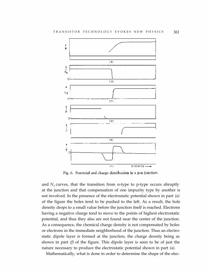
Under conditions of thermal equilibrium no net current of either holes orelectrons will flow across the junction. It is advantageous, however, to con-sider this equilibrium situation as arising from compensating currents. Weshall illustrate this by considering the flow of holes back and forth acrossthe junction. Although the density of holes is small in the n-region, it is stillappreciable and plays a vital role in the behavior of the p-n junction. Let usconsider the course of a hole that arrives in the n-region by climbing thepotential hill as illustrated in Fig. 7. Having climbed the hill and arrived atthe plateau of constant electrostatic potential in the n-type region, it willthen proceed to move by a random diffusive motion. The most probableoutcome of this motion will be that it will diffuse to the steep part of the
T R A N S I S T O R T E C H N O L O G Y E V O K E S N E W P H Y S I C S 363
hill and slide back down into the p-type region. We shall not be concernedwith holes which follow this particular course. On the other hand, it may,by chance, diffuse more deeply into the n-type region. In this event, it willon the average diffuse for lifetime τ, and subsequently it will be capturedby a deathnium center in which it recombines with an electron.
The average depth to which holes diffuse in the n-type region dependsupon the lifetime. The holes spread out in the region by diffusion. Whenthe suitable differential equation describing this process is solved, it is foundthat the average depth to which they penetrate is given by the equation.
where L is known as the diffusion length, D is the diffusion constant forholes, and τ is the lifetime for holes in the n-region. Thus under equilibriumconditions a current of holes flows from the p-region into the n-region andpenetrates on the average one diffusion length L before recombining withelectrons.
Under equilibrium conditions a principle of detailed balance holds. Thisprinciple of statistical mechanics says that each process and its opposite occurequally frequently. Hence we must conclude that the flow of holes from thep-region into the n-region, followed by recombination, must be exactlybalanced by a reverse process. The reverse process is thermal generation ofholes through deathnium centers, followed by diffusion to barrier wherethey slide down into p-type region.
The application of voltage to the terminals of the device shown in Fig. 5destroys the exact balance of the two currents just discussed. In consideringthe application of voltage we shall neglect any voltage drops at the contactsbetween the metal electrodes of Fig. 5 and the semiconductors. At the endof this section we will return briefly to the reasons why such voltage dropsmay be neglected. The effect of the application of voltages upon the currentsis represented in Fig. 8. In part (a) of this figure we show the thermalequilibrium condition. The two currents previously discussed are represent-ed by If and I g, these currents standing, respectively, for the current of holesentering the n-region and recombining and the current generated in the n-region and diffusing to the barrier2 1. For the condition of thermal equilib-rium these two currents are equal and opposite. In part (b) of the figure thesituation for a large « reverse » bias is shown. For reverse bias, negative volt-age is applied to the p-region and positive to the n-region so that the electro-

364 1 9 5 6 W . S H O C K L E Y
static potential difference between the two regions is increased. If the electro-static potential is sufficiently high, corresponding to the situation shown inpart (b), then practically no holes can climb the potential hill and If dropsnearly to zero. This situation is represented by showing If as a vector ofnegligible length, whereas Ig has practically the same value as it has for thecase of thermal equilibrium. In general, the diffusion length L is large com-pared to the width of the dipole or space-charge region. Hence the regionwhere Ig, arises is practically unaffected by reverse bias and Ig is thus inde-pendent of reverse bias. This independence of current upon bias is referredto as saturation.
When forward bias is applied, the situation shown in Fig. 8 (c) occursand If increases. This increase is described in terms of the energy differencefor a hole in the n-region and p-region. This energy difference is equal tothe charge of the electron times the electrostatic potential differences be-

T R A N S I S T O R T E C H N O L O G Y E V O K E S N E W P H Y S I C S 365
tween the two sides. We can apply a general theorem from statistical mechan-ics to a consideration of the number of holes which, by chance, acquiresufficient energy to climb the potential hill. This theorem states that eachtime the potential hill is increased by one thermal unit of energy, kT, thenthe number of holes capable of climbing the higher hill is reduced by afactor of I/e. Since the potential barrier is already present under conditionsof thermal equilibrium, it follows also that each lowering of the barrier byan amount kT will increase the current by a factor of e. The change in heightof the barrier caused by the applied voltage V is - qV, where the polarityis so chosen that positive values correspond to plus potentials applied to thep-region and q is the absolute value of the charge of the electron. V = 0is the equilibrium case, and for this case If is equal to Ig. Hence, in general,the recombination current is
I f = I g exp qV / k T
This gives rise to a total current of holes from p-region to n-region, givenby the difference
I f - I g = Ig [ e x p ( q V / k T ) - I ]
This current is zero when V = 0, increases exponentially to large values forpositive V, and decreases to a negative saturation value of Ig when V is neg-ative and substantially larger than kT/q.
Similar reasoning can be applied to the electron current flowing across thejunction. The applied potential which lowers the potential barrier for holes,evidently lowers it also for electrons; consequently, large electron currentsflow under the same voltage conditions that produce large hole currents. Inboth cases these large currents correspond to flows of minority carriers intoeach region. In both cases the current is in the sense of transferring positivecharge from the p-region to the n-region. In one case this is carried in theform of positive imperfections, namely holes, moving from p to n, and inthe other case it is due to negative imperfections, electrons, moving in theopposite direction. For the case of reverse biases the potential rise is largerand the holes tend to be retained in the p-region and the electrons in the n-region. A saturation current due to generation in both regions flows. If thetotal saturation current is called Is, then the total current for any appliedvoltage V is given by the formula
I = [exp (qV/kT)-I] I s

366 1 9 5 6 W . S H O C K L E Y
Fig. 9. Rectification characteristic for a p-n junction.
Evidently, Is, is the sum of the two generation currents. This equation isfound to be well-satisfied for p-n junctions in germanium, and a comparisonof the rectification curve22 as measured with the theoretical formula is givenin Fig. 9. It should be noted that the separation between the forward andreverse branches of the curves corresponds to a factor of e when the voltageis kT/q = 25 mV. This is exactly the factor predicted by the preceding equa-tion. This agreement between theory and experiment is evidence that theimperfections which carry the current in a p-n junction have the charge ofthe electron. If they had twice this charge, a value of 12.5 mV should beobtained; if half the charge, the value should be 50 mV.
For large forward biases, the potential barrier between the n- and p-typeis nearly eliminated. Under these conditions large concentrations of minor-ity carriers flow across the barrier and density of the majority carriers maybe substantially disturbed. Under these conditions it is no longer valid toconsider that the minority carriers diffuse in a field-free region, as is the casewhen nearly equilibrium carrier densities exist. Although these large signalconditions are of general interest, we shall not consider them further here.
There are a number of ways in which the diffusion theory for rectificationin the p-n junction can be tested experimentally. We shall consider a test
T R A N S I S T O R T E C H N O L O G Y E V O K E S N E W P H Y S I C S 367
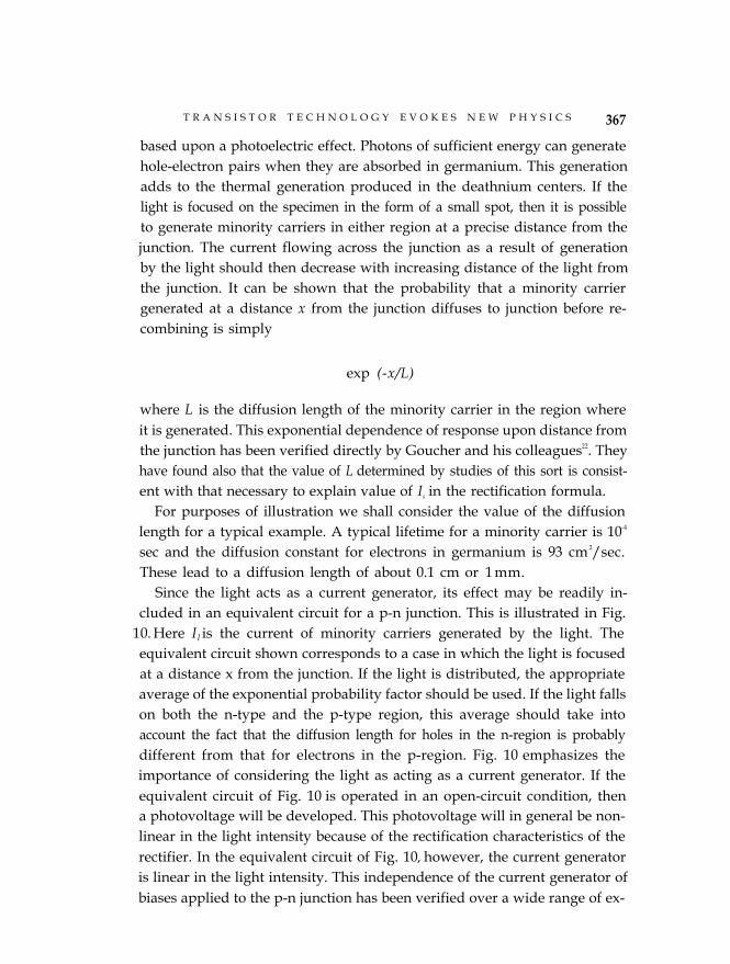
based upon a photoelectric effect. Photons of sufficient energy can generatehole-electron pairs when they are absorbed in germanium. This generationadds to the thermal generation produced in the deathnium centers. If thelight is focused on the specimen in the form of a small spot, then it is possibleto generate minority carriers in either region at a precise distance from thejunction. The current flowing across the junction as a result of generationby the light should then decrease with increasing distance of the light fromthe junction. It can be shown that the probability that a minority carriergenerated at a distance x from the junction diffuses to junction before re-combining is simply
exp (-x/L)
where L is the diffusion length of the minority carrier in the region whereit is generated. This exponential dependence of response upon distance fromthe junction has been verified directly by Goucher and his colleagues22. Theyhave found also that the value of L determined by studies of this sort is consist-ent with that necessary to explain value of Is in the rectification formula.
For purposes of illustration we shall consider the value of the diffusionlength for a typical example. A typical lifetime for a minority carrier is 10-4
sec and the diffusion constant for electrons in germanium is 93 cm2/sec.These lead to a diffusion length of about 0.1 cm or 1 mm.
Since the light acts as a current generator, its effect may be readily in-cluded in an equivalent circuit for a p-n junction. This is illustrated in Fig.
10. Here Il is the current of minority carriers generated by the light. Theequivalent circuit shown corresponds to a case in which the light is focusedat a distance x from the junction. If the light is distributed, the appropriateaverage of the exponential probability factor should be used. If the light fallson both the n-type and the p-type region, this average should take intoaccount the fact that the diffusion length for holes in the n-region is probablydifferent from that for electrons in the p-region. Fig. 10 emphasizes theimportance of considering the light as acting as a current generator. If theequivalent circuit of Fig. 10 is operated in an open-circuit condition, thena photovoltage will be developed. This photovoltage will in general be non-linear in the light intensity because of the rectification characteristics of therectifier. In the equivalent circuit of Fig. 10, however, the current generatoris linear in the light intensity. This independence of the current generator ofbiases applied to the p-n junction has been verified over a wide range of ex-

Fig. 10. Equivalent circuit for a p-n junction photocell.
The junction transistor is a compositional structure composed of two p-njunctions placed back to back. In its general behaviour as an amplifying de-vice, a junction transistor shows great similarities to a vacuum-tube triode,or thermionic valve. Fig. 11 shows an n-p-n junction transistor in an am-plifying circuit, the transistor being in the form of a sandwich with a layerof p-type germanium interposed between two layers of n-type germanium.Non-rectifying electrical contacts are made to the three layers. Under op-erating conditions the n-type region on the right, known as the collector,is biased positive so as to become attractive to electrons. As a result, a reversebias appears between it and the middle region, known as the base. The cur-rent flowing across this reverse-biased junction can be controlled by an inputsignal applied between the base layer and the n-type region to the left,known as the emitter. As I shall describe below in more detail, the bias acrossthe emitter junction controls the electron flow into the base region. In effect,the emitter junction acts like the region between the cathode and the gridin the vacuum tube. Electrons which enter the base region have a high prob-ability of diffusing to the collector junction, and thus the flow of electronsfrom emitter to collector can be varied by varying the potential across theemitter base junction. The action is very similar to that controlling the flowof electrons from the cathode to the anode in the thermionic triode.
Junction transistors can be fabricated in a variety of ways. The composi-tional structure can be produced in a crystal-growing machine by techniqueslike those used for making simple p-n junctions. As the crystal is grown froma melt containing antimony, a pellet containing indium is dropped into themelt, and a second pellet containing antimony is dropped in a few secondslater. The portion of the crystal which grows between the dropping of thetwo pellets is rich in indium and is consequently p-type. The second pellet

T R A N S I S T O R T E C H N O L O G Y E V O K E S N E W P H Y S I C S 369
Fig. 11. The structure of a junction transistor and the bias supply for its operation inan amplifying circuit.
over-compensates the effect of the added indium and the subsequent materialis again n-type. From such a single crystal small rods may be cut and con-tacts made. There are a number of technical processes involved in proceedingfrom the point of growing the crystal to the production of a packaged, stabletransistor. I shall not endeavor to discuss these in the lecture.
An alternative technique for producing the compositional structure25a
starts with a thin plate of germanium which subsequently plays the role ofthe p-type region. A pellet of metal containing a donor is placed on thisplate. The plate and pellet are then raised to such a temperature that themetal melts and dissolves a small amount of germanium. When the metaland germanium are subsequently cooled, the germanium precipitates fromthe metal and grows back onto the crystal structure of the base material.This regrown germanium carries with it some of the donors contained inthe molten metal and thus grows an n-type region. In the fabrication of atransistor, pellets are placed on both sides of a thin plate and allowances aremade for the degree to which they dissolve germanium on the two sides.This process has been used in the production of a large fraction, if not themajority, of transistors made to date.
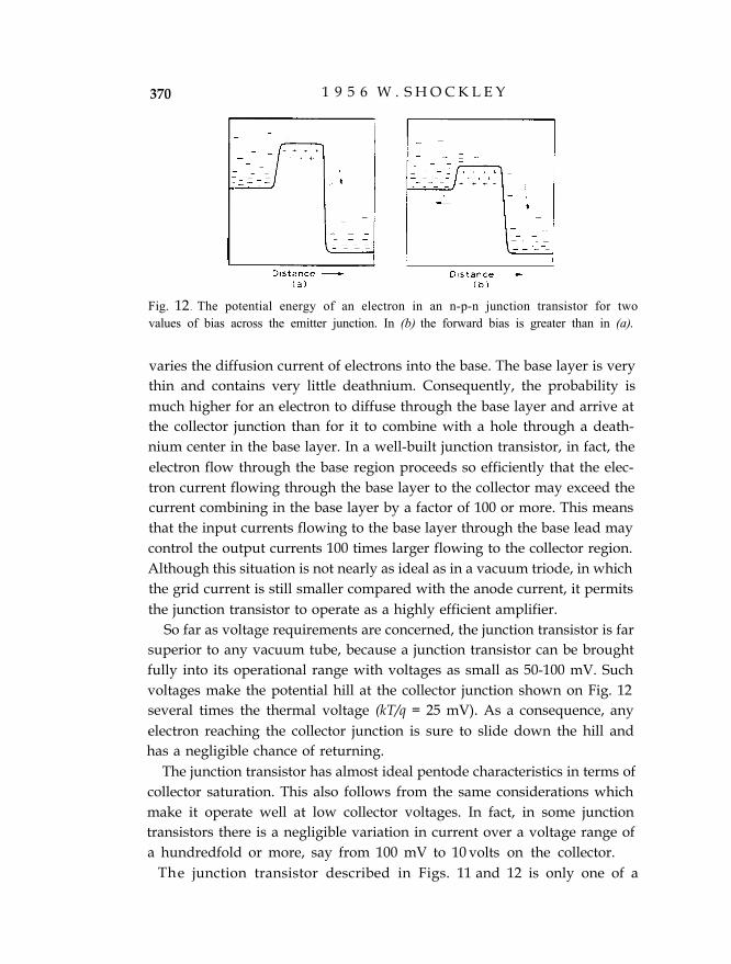
From the point of view of an electron the situation in an operating tran-sistor is as represented in Fig. 12. This diagram shows the variation in po-tential energy for an electron along a line going from emitter to collector ina transistor biased like that shown in Fig. 11. The reverse bias at the collectorjunction produces a large drop in potential on the right-hand side. The vary-ing bias across the emitter junction changes the height of the hill and thus
370 1 9 5 6 W . S H O C K L E Y
Fig. 12 . The potential energy of an electron in an n-p-n junction transistor for twovalues of bias across the emitter junction. In (b) the forward bias is greater than in (a).
varies the diffusion current of electrons into the base. The base layer is verythin and contains very little deathnium. Consequently, the probability ismuch higher for an electron to diffuse through the base layer and arrive atthe collector junction than for it to combine with a hole through a death-nium center in the base layer. In a well-built junction transistor, in fact, theelectron flow through the base region proceeds so efficiently that the elec-tron current flowing through the base layer to the collector may exceed thecurrent combining in the base layer by a factor of 100 or more. This meansthat the input currents flowing to the base layer through the base lead maycontrol the output currents 100 times larger flowing to the collector region.Although this situation is not nearly as ideal as in a vacuum triode, in whichthe grid current is still smaller compared with the anode current, it permitsthe junction transistor to operate as a highly efficient amplifier.
So far as voltage requirements are concerned, the junction transistor is farsuperior to any vacuum tube, because a junction transistor can be broughtfully into its operational range with voltages as small as 50-100 mV. Suchvoltages make the potential hill at the collector junction shown on Fig. 12several times the thermal voltage (kT/q = 25 mV). As a consequence, anyelectron reaching the collector junction is sure to slide down the hill andhas a negligible chance of returning.
The junction transistor has almost ideal pentode characteristics in terms ofcollector saturation. This also follows from the same considerations whichmake it operate well at low collector voltages. In fact, in some junctiontransistors there is a negligible variation in current over a voltage range ofa hundredfold or more, say from 100 mV to 10 volts on the collector.
The junction transistor described in Figs. 11 and 12 is only one of a
T R A N S I S T O R T E C H N O L O G Y E V O K E S N E W P H Y S I C S 371
large family of transistors. The p-n-i-p and n-p-i-n transistors are variationsof this form especially designed for low capacitance between the collectorand the base25b. The so-called junction tetrode is a special form of junctiontransistor in which the current flow is controlled so as to occur only over asmall region of the base25c. Junction transistors of these types have been usedin oscillating circuits at frequencies as high as 1000 MC/S.
In closing this section, I should like to point out that the junction transistoroperates more flexibly in terms of power than do vacuum tubes. This is ofgreat importance, since it means that junction transistors may be used effi-ciently in some cases where the power level to be amplified is very muchsmaller than the heater current required in the most efficient of vacuumtubes. The possibility of operating at very low power is due to the low volt-ages necessary to operate a junction transistor, and because of its small sizeand the high degree of purity possible, the current due to generation bydeathnium centers can be made smaller than a microampere. It is thus pos-sible to make a junction transistor which can be put into an amplifying con-dition with a power input substantially less than a microwatt. The sametransistor, however, can operate at voltages as high as 10 volts and currentsof the order of 10 mA. Thus, it can cover a power range effectively of100,000. This fact indicates that there will probably be a much smaller diver-sity of transistor types than there are of vacuum tube types.
In a lecture of reasonable scope, it is no longer possible to do justice to themany branches of semiconductor physics that have developed since the dis-covery of the transistor effect. In the previous sections I have tried to il-lustrate how the stimulation of aiming for practical goals led to an exper-imental program which brought out many new and important aspects ofelectronic phenomena in semiconductors.
Not all of the important work has, of course, been motivated by highlypractical ends which could be so immediately achieved once the fundamen-tal science was understood. Much of the work on surface states8,26 shouldnow be regarded as being in the pure-science class inasmuch as it is not pos-sible to see at all directly how the scientific results will find utility. How-ever, it seems highly probable that once the phenomena of surface states arethoroughly understood from a scientific point of view, many useful sug-

372 1 9 5 6 W . S H O C K L E Y
gestions will arise as to how this knowledge may be employed to makebetter devices.
Also in the class of purely scientific work are the very beautiful determina-tions of the energy band structure in silicon and germanium that have result-ed from cyclotron resonance in silicon and germanium27,28,29 . This work hasled to a more detailed knowledge of energy band surfaces than has everexisted before, except possibly for some of the most simple and almost trivialcases.
One of the large new areas that has begun to grow as a result of the largeamount of transistor technology may be called « The Theory of Solid Solu-tions in Silicon and Germanium ». Recently, interactions between donors andacceptors of various types have been given active consideration30. It is evi-dent that interesting phenomena are associated with the incorporation ofany foreign element from the Periodic Table in silicon and germanium.Important distinctions are being drawn between the same atoms in a sub-stitutional position and an interstitial position. It is also being found that someatoms may exist in a semiconductor in not merely two states of charge as inthe case of a simple donor and acceptor but in as many as four different con-ditions of charge31. It seems highly probable that this area of work will be-come a field of active interest in physical chemistry in the years to come.
Among the phenomena motivated in considerable measure by practicalaims we should mention the phenomena of avalanche breakdown which isuseful in voltage limiting diodes and protection devices. A strong motivationfor following up early leads which suggested that such effects might occur,came from the conversation I once had with Dr. O. E. Buckley, whom Ihave mentioned before in this lecture. Dr. Buckley pointed out the needfor a device for protecting telephones from damage due to voltages inducedby lightning near telephone lines. It was in large measure my knowledgeof this need that gave emphasis to this work. The original interpretations32
which appeared to be consistent with the dielectric breakdown mechanismonce proposed by Zener33 (direct rupture of electron-pair bonds by strongelectric fields with the resultant production of hole-electron pairs) seemsnow to have been in error. The investigation of the same phenomena byMcKay34 and his collaborators has led to a new branch of semiconductorelectronics dealing with impact ionization of holes in electrons moving inintense electric fields in semiconductors. Both the effect and its theory areplaying an active role in a certain class of switching transistors.
In closing this lecture, I would like to refer to a paragraph written in my

T R A N S I S T O R T E C H N O L O G Y E V O K E S N E W P H Y S I C S 373
book in 195035. I am pleased to see that the predictions of the paragraphappear to have been borne out to a considerable extent and I feel that it isnow as appicable as it was then:
« It may be appropriate to speculate at this point about the future of tran-sistor electronics. Those who have worked intensively in the field share theauthor’s feeling of great optimism regarding the ultimate potentialities. Itappears to most of the workers that an area has been opened up comparableto the entire area of vacuum and gas-discharge electronics. Already severaltransistor structures have been developed and many others have been ex-plored to the extent of demonstrating their ultimate practicality, and stillother ideas have been produced which have yet to be subjected to adequateexperimental tests. It seems likely that many inventions unforeseen at presentwill be made based on the principles of carrier injection, the field effect, theSuhl effect, and the properties of rectifying junctions. It is quite probablethat other new physical principles will also be utilized to practical ends as theart develops. »
It is my hope to contribute to the fulfilment of the predictions of thisparagraph through my new organization in California.
1. J. Bardeen, Nobel Lecture, this volume, p. 318.1a. J. H. Scaff, H. C. Theurer, and E. E. Schumacher, Trans. AIME, 185 (1949) 383.2. W. Shockley, Electrons and Holes in Semiconductors, D. Van Nostrand Co., Inc.,
New York, 1950, Ch. 12.3. K. Lark-Horovitz, Semi-Conducting Materials, Butterworth Scientific Publications,
London, 1951, pp. 47-48.4. J. A. Burton, G. W. Hull, F. J. Morin, and J. C. Severiens, J. Phys. Chem., 5 7
(1953) 853-859.5. The theory of this process has been developed by W. Shockley and W. T. Read,
Jr., in Phys. Rev., 87 (1952) 835-842. Experimental findings in agreement with thetheory have been obtained by Burton, Hull, Morin, and Severiens (Ref. 4) and byR. N. Hall, Phys. Rev., 83 (1951) 228; Ibid., 87 (1952) 387.
6. J. Bardeen, Phys. Rev., 71 (1947) 717-727.7. W. Shockley and G. L. Pearson, Phys. Rev., 74 (1948) 232-233.8. W. H. Brattain, Nobel Lecture, this volume, p. 377.9. J. N. Shive, Phys. Rev., 75 (1949) 689-690.
10. J. R. Haynes and W. Shockley, Phys. Rev., 75 (1949) 691.11. J. R. Haynes and W. Shockley, Phys. Rev., 81 (1951) 835-843.
J. R. Haynes and W. Westphal, Phys. Rev., 85 (1952) 680.12. Transistor Teacher’s Summer School, Phys. Rev., 88 (1952) 1368-1369.

374 1 9 5 6 W. S H O C K L E Y
13. H. Krömer, Z. Physik, 134 (1953) 435-450.14. W. Shockley, Bell System Tech. J., 33 (1954) 799-526.15. E. J. Ryder and W. Shockley, Phys. Rev., 81 (1951) 139-140.
16. E. J. Ryder, Phys. Rev., 90 (1953) 767-769.17. W. Shockley, Bell System Tech. J., 30 (1951) 990-1034.18. W. Shockley, Bell System Tech. J., 28 (1949) 435.19. G. K. Teal and J. B. Little, Phys. Rev., 78 (1950) 647.20. W. G. Pfann, Trans. AIME, 194 (1952) 747; W. G. Pfann and K. M. Olsen, Phys.
Rev., 89 (1953) 322; Bell Lab. Record, 33 (1955) 201.
21. The subscripts f and g may be thought of as forward and generation. This mixedchoice avoids subscript r, which might be either reverse or recombination. In thisdecision, forward is equivalent to recombination and generation to reverse.
22. F. S. Goucher et al., Phys. Rev., 81 (1951) 637.23. W. J. Pietenpol, Phys. Rev., 82 (1951) 120.24. W. Shockley, M. Sparks, and G. K. Teal, Phys. Rev., 83 (1951) 151.
25. W. J. Pietenpol and R. L. Wallace, Proc. I.R.E., 39 (1951) 753.25a. R. N. Hall and W. C. Dunlap, Phys. Rev., 80 (1950) 467.25b. J. M. Early, Bell System Tech. J., 33 (1954) 517.25c. R. L. Wallace, L. G. Schimpf, and E. Dickten, Proc. I.R.E., 40 (1952) 1395.26. For a recent review and references, see R. H. Kingston (Ed.), Semiconductor Surface
Physics, University of Pennsylvania Press, Philadelphia, 1957.
27. W. Shockley, Phys. Rev., 90 (1953) 491.28. G. Dresselhaus, A. F. Kip, and C. Kittel, Phys. Rev., 92 (1953) 827. R. N. Dexter,
B. Lax, A. F. Kip, and G. Dresselhaus, Ibid., 96 (1954) 222.
29. R. N. Dexter, H. J. Zeiger, and B. Lax, Phys. Rev., 104 (1956) 637-644 (ref-erences ) .
30. H. Reiss, C. S. Fuller, and F. J. Morin, Bell System Tech. J., 35 (1956) 535-636.31. H. H. Woodbury and W. W. Tyler, Phys. Rev., 105 (1957) 84.32. K. B. McAfee, E. J. Ryder, W. Shockley, and M. Sparks, Phys. Rev., 83 (1951) 650.33. C. Zener, Proc. Roy. Soc. London, A 145 (1934) 523.34. K. G. McKay, Phys. Rev., 94 (1954) 877.
35. W. Shockley, Electrons and Holes in Semiconductors, D. Van Nostrand C O ., Inc.,New York, 1950, p. 349.