transistor and it's working principle
TRANSCRIPT
Prepared ByEkram Bin Mamun – ET121002
Joyjit Das – ET121003Iftekhar Hossain – ET121007
Research Methodology
Contents
Introduction History Transistor Types Bipolar Junction Transistor (BJT) BJT Construction BJT Types & Circuit Symbol Transistor Action (NPN & PNP) Importance Of Transistor Action Hydraulic analogy of a transistor Applications
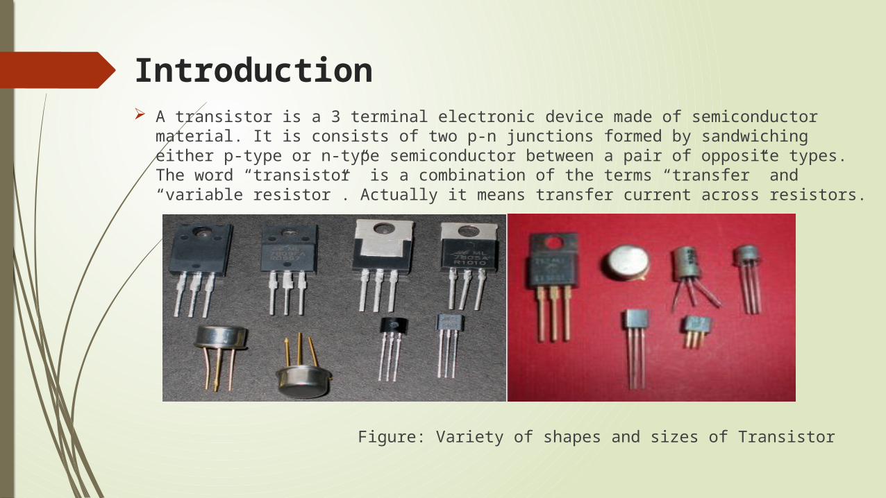
Introduction A transistor is a 3 terminal electronic device made of semiconductor material. It is
consists of two p-n junctions formed by sandwiching either p-type or n-type semiconductor between a pair of opposite types. The word “transistor” is a combination of the terms “transfer” and “variable resistor”. Actually it means transfer current across resistors.
Figure: Variety of shapes and sizes of Transistor
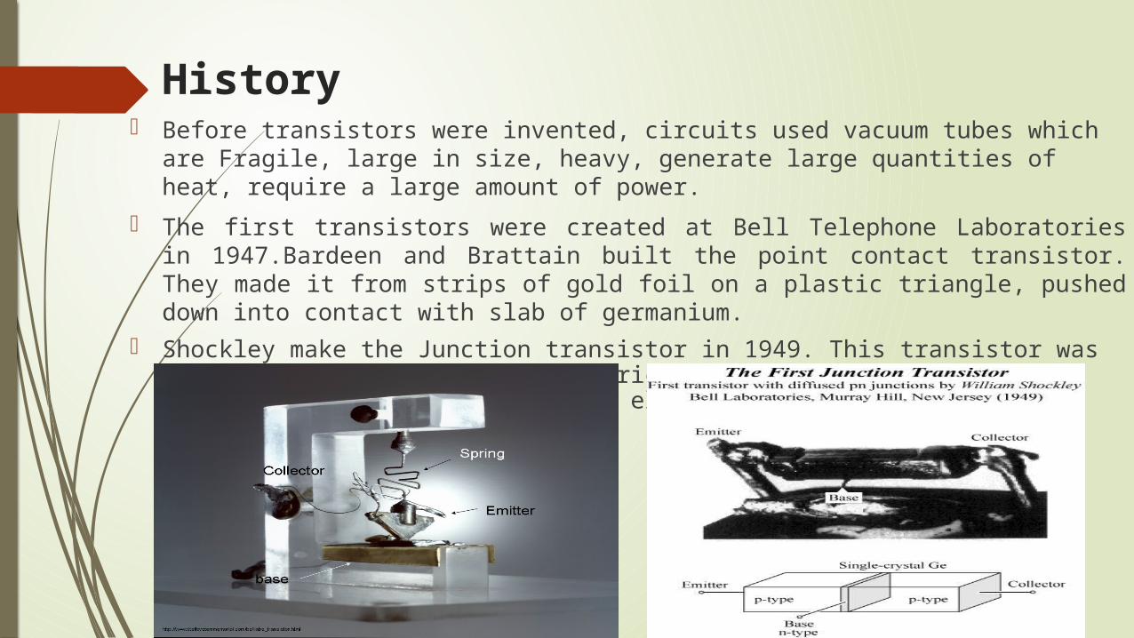
History Before transistors were invented, circuits used vacuum tubes which are Fragile,
large in size, heavy, generate large quantities of heat, require a large amount of power.
The first transistors were created at Bell Telephone Laboratories in 1947.Bardeen and Brattain built the point contact transistor. They made it from strips of gold foil on a plastic triangle, pushed down into contact with slab of germanium.
Shockley make the Junction transistor in 1949. This transistor was more practical and easier to fabricate. The Junction Transistor became the central device of the electronic age and overcome the problems of vacuum tubes.
Transistor Types Two basic types of transistors, which differ in construction and usage
(but not in main purpose) Bipolar Junction Transistors (BJTs) Field Effect Transistors (FETs)
There are other types of transistors also available in markets such as: Metal Oxide Semiconductor Field Effect Transistors
(MOSFETs)/IGFET Metal Semiconductor Field Effect Transistors (MESFETs) Darlington Transistors Photo Transistors Unijunction Transistor (UJTs) Insulated Gate Bipolar Transistors (IGBTs). Etc….
We will discuss here about Bipolar Junction Transistors
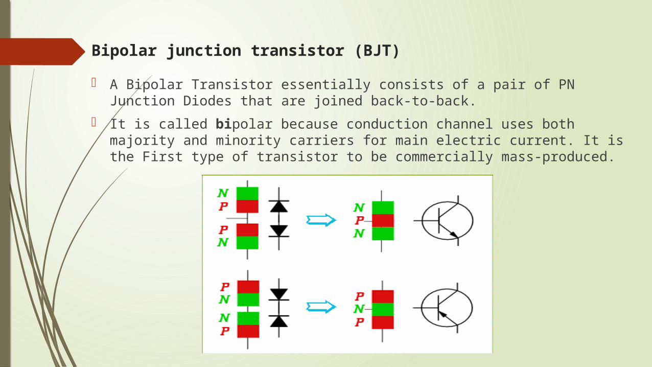
Bipolar junction transistor (BJT) A Bipolar Transistor essentially consists of a pair of PN Junction Diodes that are
joined back-to-back. It is called bipolar because conduction channel uses both majority and
minority carriers for main electric current. It is the First type of transistor to be commercially mass-produced.

BJT Construction A BJT consists of three differently doped semiconductor regions, the emitter region,
the base region and the collector region. Each semiconductor region is connected to a terminal, appropriately labelled: emitter (E),base (B) and collector (C).Two p-n junctions exist inside the BJT: collector-base junction and base-emitter junction.
The emitter is heavily doped so that it can inject(emit) a large number of charge carriers (electrons or holes) into the base. The base is lightly doped and very thin ; it passes most of the emitter injected charge carriers to the collector. The collector is moderately doped. It 'collects' charge carriers again once they've passed through the Base.
Original Manufacture
BJT Types & Circuit Symbols
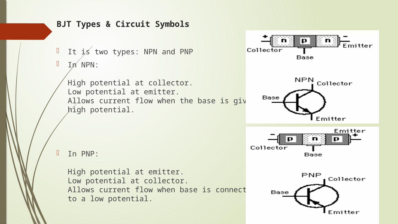
It is two types: NPN and PNP In NPN:
High potential at collector.Low potential at emitter.Allows current flow when the base is given a high potential.
In PNP:
High potential at emitter.Low potential at collector.Allows current flow when base is connected to a low potential.
Transistor Action The emitter-base junction of a transistor is forward biased whereas collector-base
junction is reverse biased. If for a moment, we ignore the presence of emitter-base junction, then practically no current would flow in the collector circuit because of the reverse bias. However, if the emitter-base junction is also present, then we will see the following:
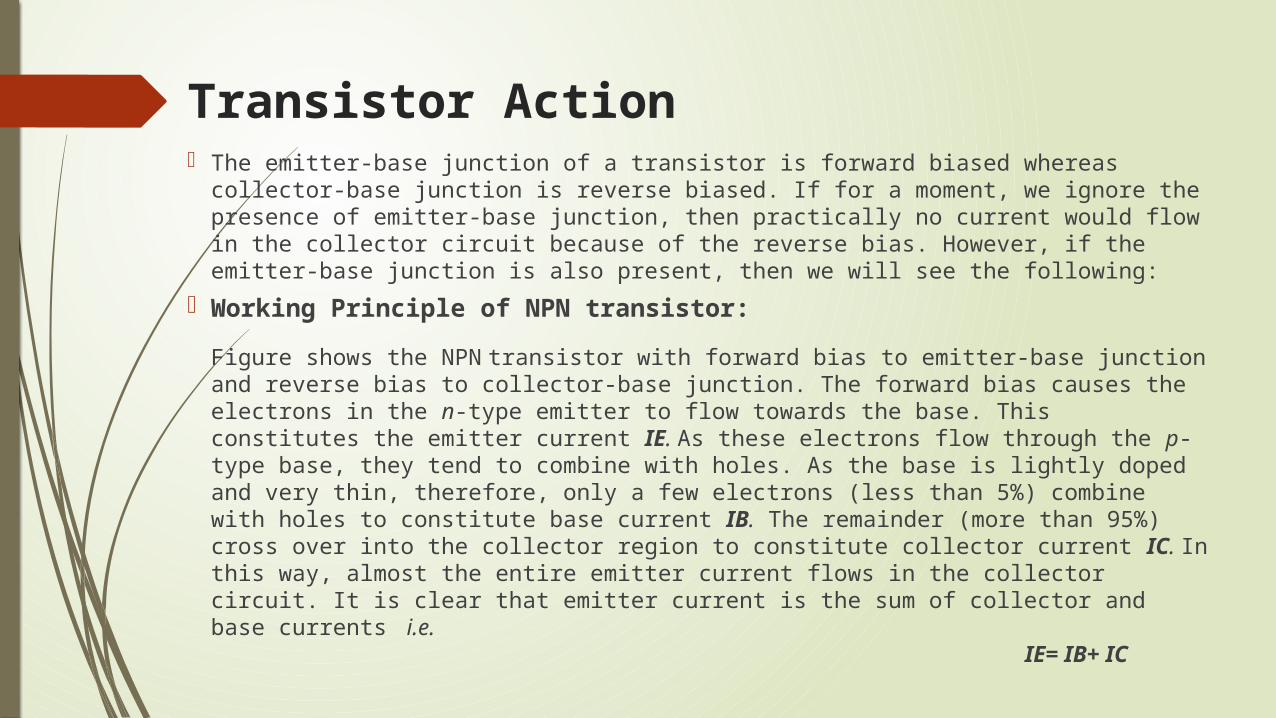
Working Principle of NPN transistor:Figure shows the NPN transistor with forward bias to emitter-base junction and reverse bias to collector-base junction. The forward bias causes the electrons in the n-type emitter to flow towards the base. This constitutes the emitter current IE. As these electrons flow through the p-type base, they tend to combine with holes. As the base is lightly doped and very thin, therefore, only a few electrons (less than 5%) combine with holes to constitute base current IB. The remainder (more than 95%) cross over into the collector region to constitute collector current IC. In this way, almost the entire emitter current flows in the collector circuit. It is clear that emitter current is the sum of collector and base currents i.e. IE= IB+ IC
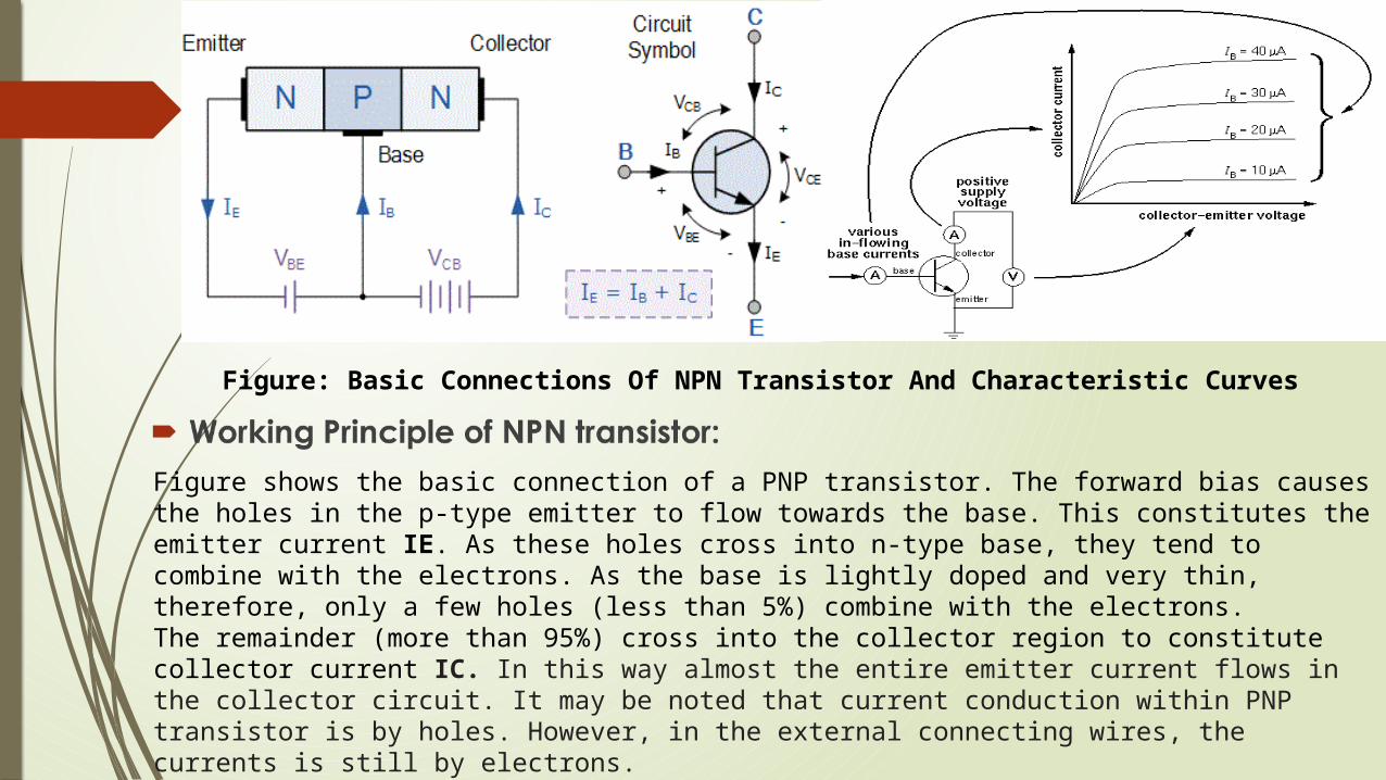
Figure: Basic Connections Of NPN Transistor And Characteristic Curves
Figure shows the basic connection of a PNP transistor. The forward bias causes the holes in the p-type emitter to flow towards the base. This constitutes the emitter current IE. As these holes cross into n-type base, they tend to combine with the electrons. As the base is lightly doped and very thin, therefore, only a few holes (less than 5%) combine with the electrons.The remainder (more than 95%) cross into the collector region to constitute collector current IC. In this way almost the entire emitter current flows in the collector circuit. It may be noted that current conduction within PNP transistor is by holes. However, in the external connecting wires, the currents is still by electrons.
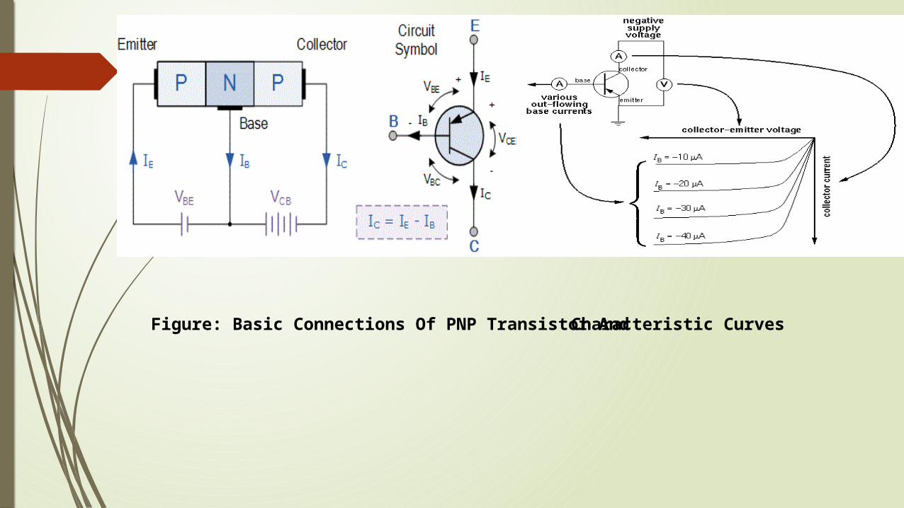
Figure: Basic Connections Of PNP Transistor And Characteristic Curves
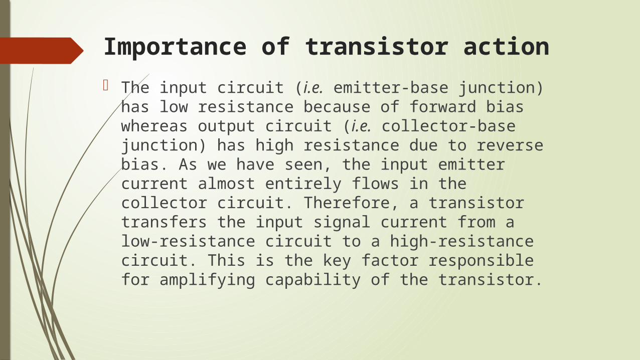
Importance of transistor action The input circuit (i.e. emitter-base junction) has low
resistance because of forward bias whereas output circuit (i.e. collector-base junction) has high resistance due to reverse bias. As we have seen, the input emitter current almost entirely flows in the collector circuit. Therefore, a transistor transfers the input signal current from a low-resistance circuit to a high-resistance circuit. This is the key factor responsible for amplifying capability of the transistor.
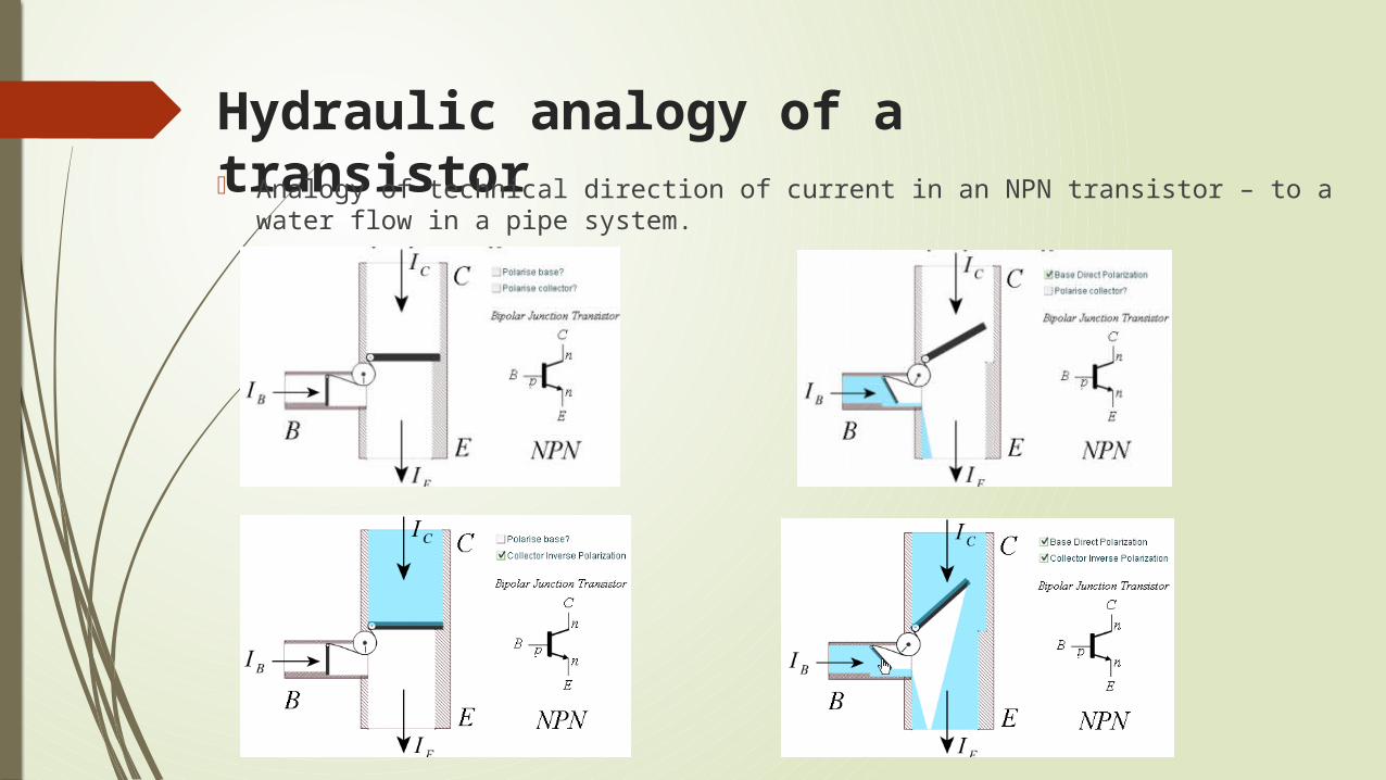
Hydraulic analogy of a transistor Analogy of technical direction of current in an NPN transistor – to a water flow in a
pipe system.
ApplicationCommon transistor applications include Amplification (Usually current amplifier but sometimes amplify voltage
also) Switching (Digital and Analog) Regulator (Voltage, Current or power) Buffer or Impedance matching between mis-matched circuits. Used in building blocks of Integrated Circuits.

The End Thank You