transistor
TRANSCRIPT

TRANSISTOR - Introduction

Introduction• Beside diodes, the most popular semiconductor devices is transistors. Eg:
Bipolar Junction Transistor (BJT)• Transistors are often said to be the most significant invention of the 20th
Century.• If cells are the building blocks of life, transistors are the building blocks of
the digital revolution. Without transistors, the technological wonders you use every day -- cell phones, computers, cars -- would be vastly different, if they existed at all.
• Transistors are more complex and can be used in many ways• Most important feature: can amplify signals and as switch • Amplification can make weak signal strong (make sounds louder and
signal levels greater), in general, provide function called Gain
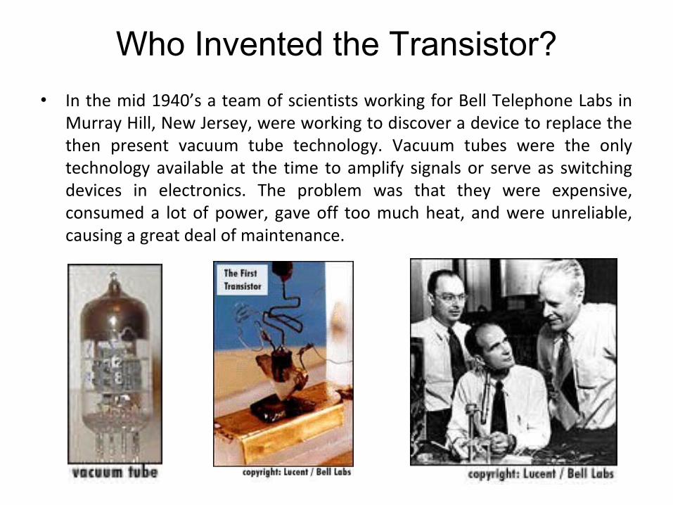
Who Invented the Transistor?• In the mid 1940’s a team of scientists working for Bell Telephone Labs in
Murray Hill, New Jersey, were working to discover a device to replace the then present vacuum tube technology. Vacuum tubes were the only technology available at the time to amplify signals or serve as switching devices in electronics. The problem was that they were expensive, consumed a lot of power, gave off too much heat, and were unreliable, causing a great deal of maintenance.

The Transistor• The scientists that were responsible for the 1947 invention of
the transistor were: John Bardeen, Walter Brattain, and William Shockley. Bardeen, with a Ph.D. in mathematics and physics from Princeton University, was a specialist in the electron conducting properties of semiconductors. Brattain, Ph.D., was an expert in the nature of the atomic structure of solids at their surface level and solid-state physics. Shockley, Ph.D., was the director of transistor research for Bell Labs.
Their original patent name for the transistor was: “Semiconductor amplifier; Three-electrode circuit element utilizing semi conductive materials.” In 1956, the group was awarded the Noble Prize in Physics for their invention of the transistor. In 1977, John Bardeen was awarded the Presidential Medal of Freedom.

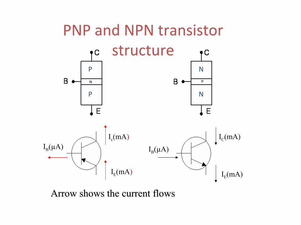
• BJT is bipolar because both holes (+) and electrons (-) will take part in the current flow through the device– N-type regions contains free electrons (negative carriers)– P-type regions contains free holes (positive carriers)
• 2 types of BJT– NPN transistor– PNP transistor
• The transistor regions are:– Emitter (E) – send the carriers into the base region and then on to the
collector– Base (B) – acts as control region. It can allow none,some or many
carriers to flow – Collector (C) – collects the carriers
Transistor Structure
P
P
P
N
N
N
PNP and NPN transistor structure
IB(µA) IB(µA)
Ic(mA)
IE(mA) IE(mA)
IC(mA)
Arrow shows the current flowsArrow shows the current flows

Transistor Construction• A transistor has three doped regions.• For both types, the base is a narrow region sandwiched between the larger
collector and emitter regions.
The emitter region is heavily doped and its job is to emit carriers into the base.
The base region is very thin and lightly doped. Most of the current carriers injected into the base pass on to the collector.
The collector region is moderately doped and is the largest of all three regions.
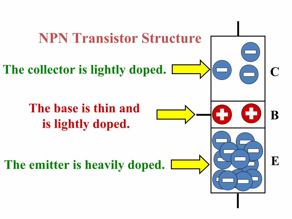
N
P
NThe collector is lightly doped. C
The base is thin and is lightly doped.
B
The emitter is heavily doped. E
NPN Transistor Structure

Transistor configuration
• Transistor configuration –is a connection of transistor to get variety operation.• 3 types of configuration:
– Common Collector.– Common Base.– Common Emitter

Common-Collector Configuration The input signal is applied to the base terminal and the output is taken
from the emitter terminal. • Collector terminal is common to the input and output of the circuit• Input – BC• Output – EC
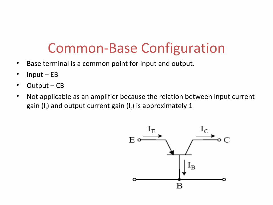
Common-Base Configuration• Base terminal is a common point for input and output.• Input – EB• Output – CB • Not applicable as an amplifier because the relation between input current
gain (IE) and output current gain (IC) is approximately 1

Common-Emitter Configuration• Emitter terminal is common for input and output circuit• Input – BE• Output – CE• Mostly applied in practical amplifier circuits, since it provides good voltage,
current and power gain
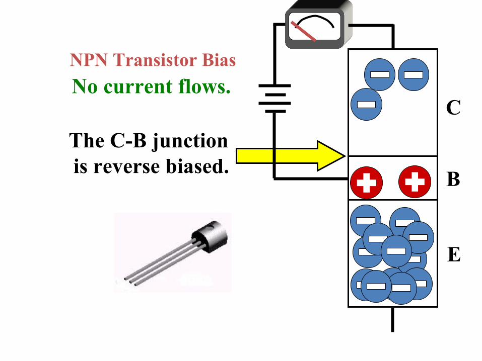
The C-B junction is reverse biased.
N
P
N
NPN Transistor Bias
C
B
E
No current flows.
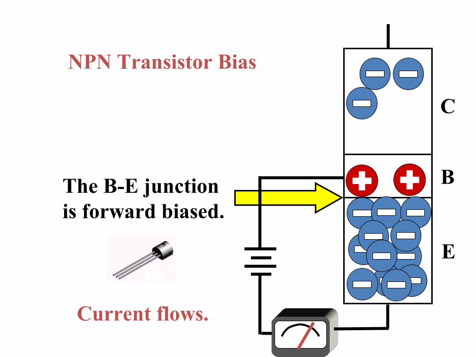
The B-E junction is forward biased.
N
P
N
NPN Transistor Bias
C
B
E
Current flows.

When both junctionsare biased....
N
P
N
NPN Transistor Bias
C
B
E
Current flowseverywhere.
Note that IB is smallerthan IE or IC.
IC
IB
IE

Transistor operation

N
P
N C
B
E
Although IB is smallerit controls IE and IC.
IC
IB
IE
Note: when the switch opens, all
currents go to zero.
Gain is something smallcontrolling something large
(IB is small).

N
P
C
B
E
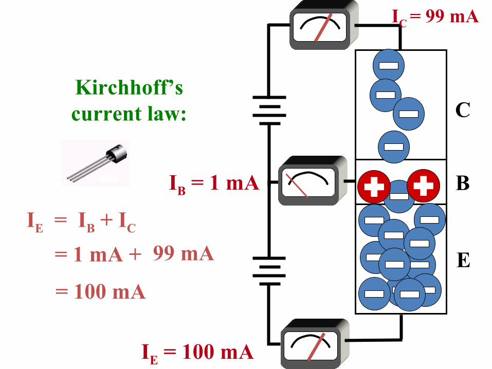
IC = 99 mA
IB = 1 mA
IE = 100 mA
β = IC
IB
The current gain frombase to collector
is called β.
99 mA
1 mA= 99
N
P
C
B
E
IC = 99 mA
IB = 1 mA
IE = 100 mA
IE = IB + IC
99 mA= 1 mA +
= 100 mA
Kirchhoff’scurrent law:
C
B
E
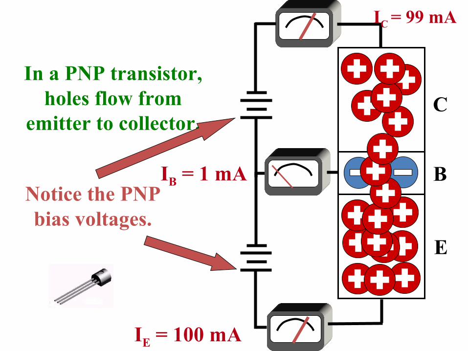
IC = 99 mA
IB = 1 mA
IE = 100 mA
In a PNP transistor,holes flow from
emitter to collector.
Notice the PNPbias voltages.
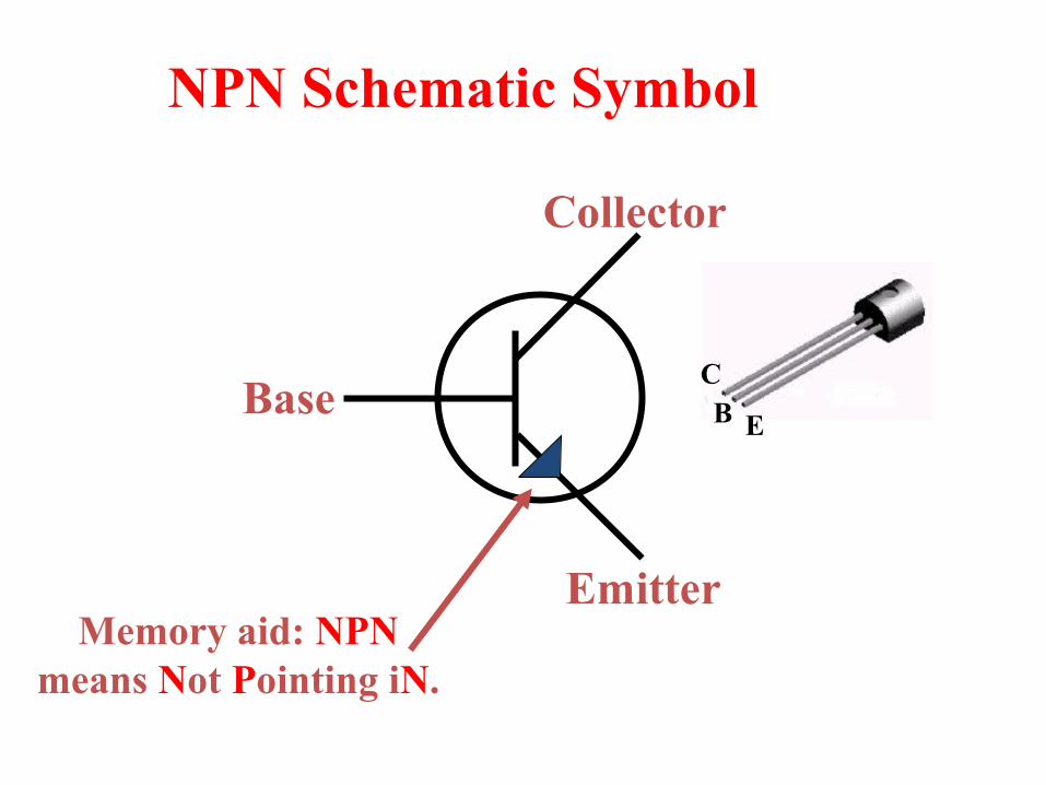
Emitter
Base
Collector
Memory aid: NPNmeans Not Pointing iN.
EBC
NPN Schematic Symbol

Collector
Base
Emitter
EBC
PNP Schematic Symbol
Memory aid: NPNmeans Pointing iN Properly.

Recall: NPN and PNP Bias
• Fundamental operation of pnp transistor and npn transistor is similar except for:
– role of electron and hole,
– voltage bias polarity, and
– Current direction
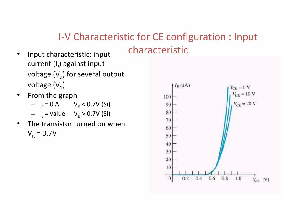
I-V Characteristic for CE configuration : Input characteristic• Input characteristic: input
current (IB) against input voltage (VBE) for several output voltage (VCE)
• From the graph – IB = 0 A VBE < 0.7V (Si)– IB = value VBE > 0.7V (Si)
• The transistor turned on whenVBE = 0.7V

I-V Characteristic for CE configuration : Output characteristic
• Output characteristic: output
current (IC) against output
voltage (VCE) for several
input current (IB)
• 3 operating regions:– Saturation region– Cut-off region– Active region

• Saturation region – in which both junctions are forward-biased and IC increase linearly with VCE
• Cut-off region – where both junctions are reverse-biased, the IB is very small, and essentially no IC flows, IC is essentially zero with increasing VCE
• Active region – in which the transistor can act as a linear amplifier, where the BE junction is forward-biased and BC junction is reverse-biased. IC increases drastically although only small changes of IB.
• Saturation and cut-off regions – areas where the transistor can operate as
a switch
• Active region – area where transistor operates as an amplifier
I-V Characteristic for CE configuration : Output characteristic

Current Relationships
• Relations between IC and IE :α = IC
IE
• Value of α usually 0.9998 to 0.9999, α ≈ 1• Relations between IC and IB :
β = IC @ IC = βIB
IB
• Value of β usually in range of 50 400• The equation, IE =IC + IB can also written in β
IC = βIB
IE = βIB + IB => IE = (β + 1)IB
• The current gain factor , α and β is: α = β @ β = α . β + 1 α - 1
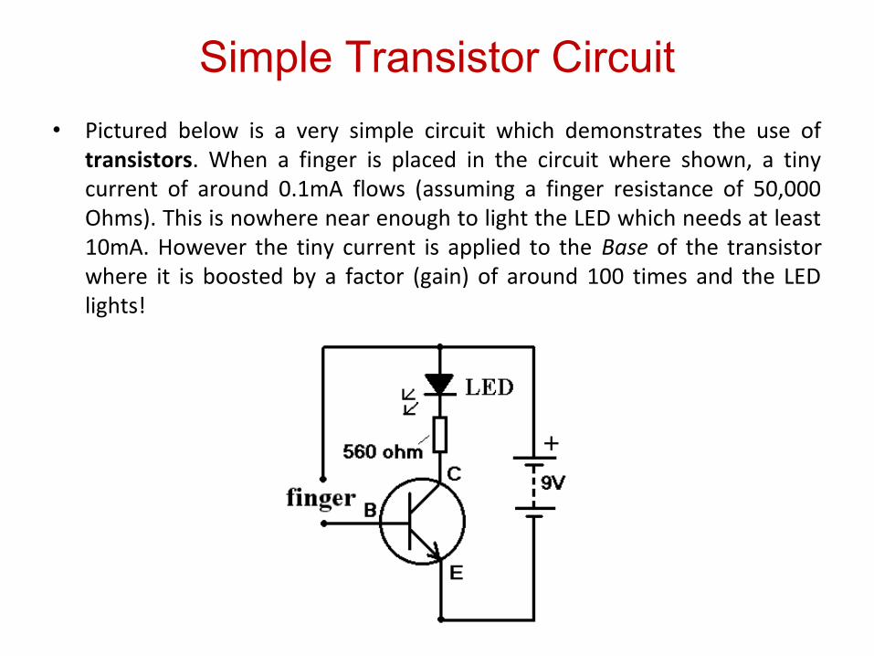
Simple Transistor Circuit• Pictured below is a very simple circuit which demonstrates the use of
transistors. When a finger is placed in the circuit where shown, a tiny current of around 0.1mA flows (assuming a finger resistance of 50,000 Ohms). This is nowhere near enough to light the LED which needs at least 10mA. However the tiny current is applied to the Base of the transistor where it is boosted by a factor (gain) of around 100 times and the LED lights!
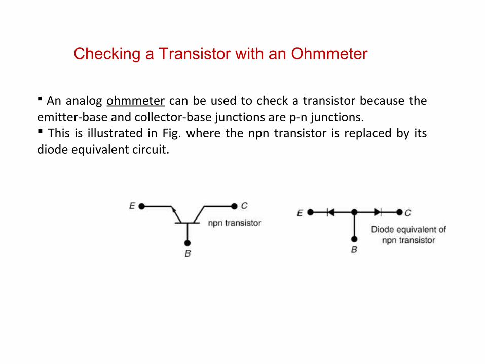
Checking a Transistor with an Ohmmeter
An analog ohmmeter can be used to check a transistor because the emitter-base and collector-base junctions are p-n junctions. This is illustrated in Fig. where the npn transistor is replaced by its diode equivalent circuit.

Checking a Transistor with an Ohmmeter
To check the base-emitter junction of an npn transistor, first connect the ohmmeter as shown in Fig. 28-9 (a) and then reverse the ohmmeter leads as shown in (b). For a good p-n junction made of silicon, the ratio RR/RF should be equal to or greater than 1000:1.
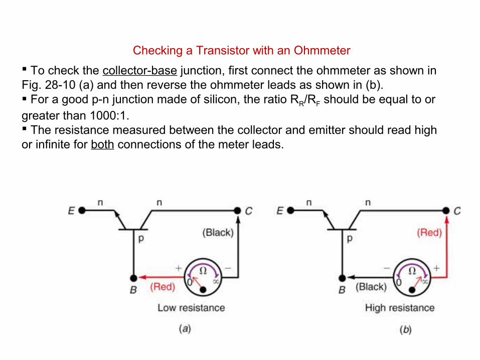
Checking a Transistor with an Ohmmeter
To check the collector-base junction, first connect the ohmmeter as shown in Fig. 28-10 (a) and then reverse the ohmmeter leads as shown in (b). For a good p-n junction made of silicon, the ratio RR/RF should be equal to or greater than 1000:1. The resistance measured between the collector and emitter should read high or infinite for both connections of the meter leads.

Checking a Transistor with an Ohmmeter
Low resistance across the junctions in both directions: transistor is shorted.
High resistance on both directions: transistor is open.
In these cases, the transistor is defective and must be replaced.