transformation of porous nanostructure and self-ordering
TRANSCRIPT

Transformation of porous nanostructure and self-ordering of anodic alumina films during potentiostatic anodising of aluminium
ABSTRACT Aluminium anodization in sulfuric acid at constant anodic potential was studied. The current density increased significantly in the second transient stage and gave successive extremes in the next quasi-steady state stage. The electrolysis voltage alike varied around the 25 V self-ordering regime. The porous anodic alumina films developed at strongly variable rate. Field emission scanning electron microscopy (FESEM) showed that the mean cell width, interpore spacing about 2.5 nm V−1 and surface density of pores change in both stages. The first two parameters increase and the third decreases with the current density in the second transient stage. However, in the quasi-steady state, the first two vary inversely and the third similarly to current density. Concurrently, incessant termination/generation of pores occur. Pores that ceased growing, pores branching inwards and dendritic/serrated ones appear and their order changes. Structure change results from pores’ termination/generation during both stages and intrinsic thinning of the barrier layer during the first. Pores’ order improves when their termination rate exceeds generation one. It is maximized when these rates are low and balanced. Current density, nanostructure, self-ordering and incessant termination/
generation of pores are strongly interdependent key factors of film growth. KEYWORDS: potentiostatic Al anodization, porous alumina films, FESEM, nanostructure-self-ordering, termination-generation of pores. 1. INTRODUCTION Over the past decades aluminium (Al) anodization has been shown to be an exciting model process for solid-state electrochemistry [1-4]. During Al anodization in pore-forming electrolytes, porous anodic alumina films (PAAF) grow [5]. In such electrolytes, e.g. oxalic, sulphuric, phosphoric, tartaric, etc. acid, PAAF grow in three sequential stages, the first and second transient stages and the steady state one. At the first stage a microscopically flat barrier layer is formed; towards its end pores are nucleated on the oxide surface and the PAAF structure is generated [6-10]. In the second stage, pores are developed and organized producing the PAAF structure [8-19] that is completed to its end [4, 20]. In the third stage, PAAF structure is reproduced. This structure is characterised as a close-packed array of about hexagonal columnar cells [1, 2, 21, 22]. Each cell contains an elongated roughly cylindrical pore perpendicular to the Al surface which extends from the metal|oxide (m|o) interface to the top surface. Between this interface and
1Laboratory of Physical Chemistry, Department of Industrial Design and Production Engineering, School of Engineering, University of West Attica, P. Ralli & Thivon 250, Egaleo, Attiki, 11244; 2Institute of Nanoscience and Nanotechnology, National Centre for Scientific Research “Demokritos”, Agia Paraskevi, Attiki, 15341, Greece.
G. Patermarakis1,* and T. M. Triantis2
*Corresponding author: [email protected]
Current Topics in Electrochemistry
Vol. 21, 2019
pore bottom a thin compact hemispherical (or hemispheroid) shell-shaped barrier-type oxide layer with thickness about 1 nm per V of applied voltage is interposed [1, 2, 21, 22]. In addition to characteristic porous nanostructure, PAAF also have specific physicochemical and mechanical properties making them suitable for numerous applications such as corrosion protection, friction resistance, decoration etc. for mechanical, civil, architectural, aircraft and aerospace engineering [3, 23, 24]. Basic requirements are normal growth of films without burning emergence, absence of mostly macroscopic defects and proper thickness and porosity. PAAF also find applications in fuel cells, rechargeable batteries, magnetic memories, nuclear reactors, templates for synthesizing emitters, nanoscience/nanotechnology, catalysis, template substrate for surface-enhanced Raman scattering (SERS) analytical technique and SERS biosensors etc. [4, 25-31] and currently developing technologies [12-17, 32]. PAAF have become a fundamental tool to develop various functional nanomaterials. The long range regular porous nanostructure with a self-ordered hexagonal or any pre-indented geometry is crucial and introduces stricter requirements. Closed-packed highly ordered pores in PAAF are formed by two step anodization usually in narrow windows of process conditions, known as “self-ordering regimes” [4, 33-35]. Work was done to explore the optimum range of the self-ordering regimes and tuning the interpore distance [36, 37], the best order anodization regimes in the first and second steps [38-43] and the effect of prolonged anodization outside the self-ordering regimes on the maintenance or not of the ordered nanostructure [44, 45]. In spite of progress so far, the central query on the real physicochemical mechanism that causes the structure ordering near the metal in the second transient stage and up to the initial range of the steady state stage in the first anodization step remains essentially unanswered. Its full elucidation actually needs much further work. PAAF growth in steady state is characterized by almost constant current or voltage during potentiostatic or galvanostatic anodization. Recently, however, it has been shown that the knowledge associated with this stage is still deficient [22, 46-48]. For example, during prolonged potentiostatic
22 G. Patermarakis & T. M. Triantis
anodization at various concentrations of H2SO4, temperatures and anodic potentials, the chronoamperometric plot shows highly variable profile and shift, while film growth is normal. In this work, one-step Al anodization is studied in a three-electrode system in H2SO4 electrolyte (0.51 M) at constant temperature (25 °C) and anodic potential (vs. SHE) 23.615 V and times up to 180 min. Despite constant anodic potential, current largely varies with time, even in the quasi-steady state stage, and the anodization voltage does alike. Also, PAAF grow at a strongly variable rate. Detailed Field Emission Scanning Electron Microscopy (FESEM) study, among others, allowed the determination of certain structural parameters such as mean cell width, interpore spacing and pore surface density and revealed incessant termination/generation of pores in the barrier layer region as well as change of pore ordering. For the first time, strong interdependence has been shown between current density change, nanostructure and self-organization transformations, and continuous termination/ generation of pores. New key details of PAAF growth mechanism are revealed, important for Al anodization electrochemistry and many PAAF applications. 2. MATERIALS AND METHODS Two-faces Al specimens with thickness 0.5 mm and purity ≥ 99.95% (Merck pro-analysis) were anodized. The dimensions of anodized surface were 3 × 3 cm2 and the corresponding entire anodized surface area (Sg) was 18.55 cm2. Anodization experiments were carried out potentiostatically in rigorously stirred H2SO4 solution at concentration (ca) = 5% w/v (or 0.51 M) and temperature (T) = 25 (± 0.1-0.2) °C. For each experiment fresh solution was used to avoid solution ageing. The necessity of three-electrode system for thorough studies of PAAF growth kinetics and mechanism was emphasized recently [46-48] and explained in detail [48]. This system consisted of Al working electrode, counter cathodic electrode (two Pb sheets symmetrically placed on either side of Al at distance 5 cm) and Hg/Hg2SO4 reference electrode attached closely and laterally to Al, with its pin mouth hole located at the

Structural characterization of porous anodic alumina films 23
For this purpose just left and right of the centre of anodized surface two adjacent symmetric pieces were carefully cut, each 1 × 1 cm2. One piece was used to examine the top surface and the cross section formed by bending the piece. In the other piece, after the selective removal of oxide by chromophosphoric acid solution [1, 2, 56], the imprint of film on the bare Al was examined. As proved earlier [22, 39] the examination of film imprint offers detailed and accurate information on the structure of m|o interface. As cells/pores ordering deviates more or less from the ideal hexagonal arrangement, the best method of finding the surface density of cells/pores near Al (n), thus the mean size of cells, is to measure the population of cells on accurately known large e.g. square surface areas of FESEM micrographs. These areas were large enough to contain at least 70-80 cells. Cell population is the total number of cells wholly contained in the selected area plus half the number of cells crossed by its boundaries considering that the cut-off cell surface areas are normally distributed around the half mean cell surface area. The number of crossed cells was many times smaller than the number of cells wholly contained. Hence the error made really tends to zero. Such measurements were made on all available micrographs with magnifications ≥ 5 × 10⁴ at each t. From cell population and corresponding surface area, the real area of the mean cell on Al surface was determined. Then the mean value was found for various micrographs at each t. This was used to determine the mean cell width (Dc) defined by the diameter of a circle with surface identical to that of mean cell section, mean cells/pores surface density near Al surface (n), mean interpore spacing (Dint), etc. 3. RESULTS
3.1. Kinetic data of PAAF growth For an in depth study of PAAF growth, basic kinetic data such as j, ΔV, mox,mb and hf,a vs. t are essential. Al anodization conditions ca = 0.51 M, T = 25 °C, Pan = 23.615 V and t’s up to 180 min were chosen, where film growth is normal (thus burning does not appear, see section 1) and distinct extremes of j appear. The plots of j and ΔV vs. t are depicted in Figures 1a-d at
middle of 3 cm height. This electrode was selected because of common anion with electrolyte. It has E0 (vs. SHE) equal to 0.615 V at T = 25 °C [49]. During Al anodization constant anodic potential (Pan) vs. reference electrode was applied, Pan − Pref = 23 V. By definition Pan > 0. At T = 25 °C, Pan (vs. SHE) = Pan = (Pan − Pref) + Pref = 23 + 0.615 = 23.615 V. The potential drop from the bottom of pores to the reference electrode is negligible compared with Pan. Thus essentially the potential drop in the barrier layer (ΔP) ≈ Pan. Plots of the anodization voltage (potential difference between anode and cathode, ΔV) vs. time (t) and chronoamperometric plots were obtained. Plots of current density (j), Pan and ΔV vs. t are usually used among others to discern the stages of PAAF growth and derive details of its mechanism. At constant Pan, even in steady state the current generally changes with t; thus it is in fact a quasi-steady state. At the employed anodization conditions, ΔV is around 25 V regime of self-ordering [16, 50] for the origin of which certain alternative views appeared recently [51-53]. The entire procedures of Al specimens’ pre-treatment, anodization, washing, neutralization, drying and desiccation were described in detail previously [46-48]. Since j varies with t, the charge (Q) and average j (ja) were found by numerical integration of j vs. t plots. The Al specimens were weighted before and after anodization (with sensitivity 10−5 g) in order to find the accurate mass of product oxide by the mass balance method (mox,mb), mox,mb = Δm + mAl,F = Δm + Q(AMAl)(3F)-1 [54], where Δm is the difference of Al anode mass after and before anodization, mAl,F is consumed Al mass by Faraday’s law and AMAl is the atomic mass of Al. The local film thickness (hf) was measured suitably at various positions on the surface of Al specimen by a non-destructive method [48] and the mean value (hf,a) was found. Then the average transport number of anions O2- in barrier layer (tnan,a) during anodization was determined by hf,a = kjatnan,at = ktnan,aQ/Sg, where k is the rate constant of thickness growth (6.9833 × 10⁻⁵ cm3 C-1) [55]. The morphology of the top surfaces, cross sections and imprints on Al substrate of PAAF were studied by FESEM (JEOL JSM -7401f).
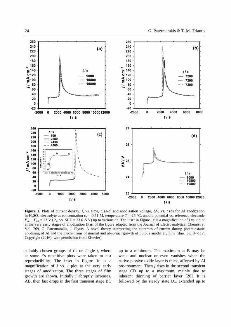
suitably chosen groups of t’s or single t, where at some t’s repetitive plots were taken to test reproducibility. The inset in Figure 1c is a magnification of j vs. t plot at the very early stages of anodization. The three stages of film growth are shown. Initially j abruptly increases, AB, then fast drops in the first transient stage BC
up to a minimum. The maximum at B may be weak and unclear or even vanishes when the native passive oxide layer is thick, affected by Al pre-treatment. Then j rises in the second transient stage CD up to a maximum, mainly due to inherent thinning of barrier layer [20]. It is followed by the steady state DE extended up to
24 G. Patermarakis & T. M. Triantis
Figure 1. Plots of current density, j, vs. time, t, (a-c) and anodization voltage, ΔV, vs. t (d) for Al anodization in H2SO4 electrolyte at concentration ca = 0.51 M, temperature T = 25 °C, anodic potential vs. reference electrode Pan − Pref = 23 V (Pan vs. SHE = 23.615 V) up to various t’s. The inset in Figure 1c is a magnification of j vs. t plot at the very early stages of anodization (Part of the figure adapted from the Journal of Electroanalytical Chemistry, Vol. 769, G. Patermarakis, J. Plytas, A novel theory interpreting the extremes of current during potentiostatic anodising of Al and the mechanisms of normal and abnormal growth of porous anodic alumina films, pg. 87-117, Copyright (2016), with permission from Elsevier).

Structural characterization of porous anodic alumina films 25
apex and 4500 s around which the strong drop of j after peak apex ends, Figure 1c. ΔV generally follows j. The reproducibility of j vs. t plot and its extremes is good and that of ΔV vs. t, considering all above t’s, and not only those in Figure 1d, was generally tolerable. Values at various t’s of certain kinetic parameters and physical/structural features related with film growth, such as the above j extremes, ja, Q, mox,mb and hf,a, appear in Table 1. The plots of mox,mb and hf,a vs. t (t ≤ 7200 s) and corresponding Q appear in Figure 2. Since at t = 7200 s three values of mox,mb, hf,a and Q are available, their mean values are used in those plots. Figure 2a shows that the rates of film growth dmox,mb/dt and dhf,a/dt vary strongly with t. The hf,a vs. Q plot is almost linear but the mox,mb vs. Q bends apparently due to chemical attack of pore walls by the electrolyte during anodization that enlarges the pores outward. At t = 9000 and 10800 s (specimens a and b), the produced film thicknesses are found by
high t’s. Detailed search of BC is avoided without injuring the analysis that focuses mainly on DE extended as above and secondarily on CD stage. Figures 1a-c show that a low broad maximum of j appears at the boundary of the second transient and quasi-steady state stages at ≈ 600 s, followed in the last stage by a shallow minimum at ≈ 1045 s and then by a sharp maximum (hereafter peak) at ≈ 2505 s. Then j decreases continuously up to some t among 7200 and 9000 s and then it slightly but clearly rises, Figure 1a. At 9000 and 10800 s, but not at t’s ≤ 7200 s, exfoliation of an outer surface layer occurred in an area enlarged with t. It started before 9000 s and was spread over most of the surface up to 10800 s. In this area locally a temporarily reduced limiting thickness is thus established. Separate plots were taken at t = 7200 s, Figure 1b, and at other characteristic t’s that are 600 s around the above boundary, 2280 s where the strong rise of j starts before peak apex, 2430 s around peak Table 1. Maximum j at the boundary of the second transient and quasi-steady state stages, jb, minimum j at the plateau in the last stage, jmin, maximum j at peak apex, jmax, charge passed from the anodized surface Sg = 18.55 cm2 of Al, Q, average current density, ja, mass of produced oxide present on Sg, mox,mb, average film thickness along Sg, hf,a, and average transport number of O2− cations in the barrier layer during anodization, tnan,a, at various anodization times, t.
t / s jb / mA cm-2
jmin / mA cm-2
jmax / mA cm-2 Q / C ja /
mA cm-2 mox,mb /
g hf,a / μm tnan,a
600 27.1 - - 280.9 25.2 0.0399 7.9 0.747 2280 26.7 25.7 - 1135.0 26.8 0.1567 32.2 0.753
2430 27.4 25.8 239.0 1577.8 35.0 0.2201 46 0.774
4500 27.5 26.1 254.3 4520.9 54.2 0.5640 143.3 0.842
7200 (sample a) 28.0 25.0 184.0 5742.8 43.0 0.6280 181.3 0.839
7200 (sample b) 26.6 25.2 240.9 5986.0 44.8 0.6237 186.3 0.827
7200 (sample c) 28.8 25.9 197.8 6058.5 45.4 0.6547 183.3 0.804
9000 27.9 25.9 188.0 7034.3 42.1 0.6406 ≈199.7a –a
10800 (sample a) 27.6 26.1 207.1 8537.9 42.6 0.5868 ≈165.3a –a
10800 (sample b) 26.4 25.3 162.4 7946.9 39.7 0.5649 ≈179.0a –a aDue to exfoliation of an outer oxide layer in a part of surface, hf,a is approximate while the tnan,a cannot be found from hf,a and t (Part of the table data adapted from the Journal of Electroanalytical Chemistry, Vol. 769, G. Patermarakis, J. Plytas, A novel theory interpreting the extremes of current during potentiostatic anodising of Al and the mechanisms of normal and abnormal growth of porous anodic alumina films, pg. 87-117, Copyright (2016), with permission from Elsevier).

around j peak apex. Then it generally improves with t but remains inferior to the order of cells at the two lower t’s. It is noted that quantitative estimate of order degree is out of the scope of this study. ΔV varies noticeably with t, around the 25 V self-ordering regime [16, 50]. However, ΔV is not the main factor controlling the order. Besides constant Pan (> 0), ΔV (> 0) includes a term that embraces the potential drop in bath solution and cathodic potential (ΔV = Pan + (potential drop in bath solution – cathodic potential), where potential drop in bath solution > 0 and cathodic potential < 0). This term varies similarly to ΔV. There is no reason why the order should be related with this term. If any, a relationship must exist with Pan. If the order depended only on Pan, it would be identical at all t’s, which is not the case. Hence other parameter(s) and linked process(es) in the region of barrier layer are responsible for self-ordering degree. The order of cells/pores is on average comparable at 600 s and 2280 s. The best order appears at t’s 600-2280 s, or around the shallow j minimum with mean value ≈ 25.7 mA cm−2 at t ≈ 1045 s, (Figures 1a-c and Table 1) where the order is expected to differ negligibly from that at 600 and 2280 s. At 9000 s it worsens slightly compared with 7200 s (sample b) and at 10800 s (sample a) it improves compared with 9000 s (Figures 3e-g).
extrapolating the plot hf,a vs. Q, Figure 2b, up to the Q’s at t = 9000 and 10800 s, Table 1. Calculated values for these film thicknesses are ≈ 220.1, 267.1 and 248.6 μm, much higher than hf,a’s in Table 1. This is due to the film surface exfoliation on an area enlarged with t establishing a temporarily reduced limiting thickness at these t’s as well as to establishment of maximum limiting thickness in the rest area at t’s > 7200 s. The first occurs when, due to the aforesaid pore wall attack, the mean pore diameter approaches the mean cell width well below the top surface and the second when this occurs around the top surface [56]. So, in both areas a significant outer portion of produced thickness has been actually removed. From the remaining hf,a’s, Table 1, and produced thicknesses, the average removed thickness is found ≈ 20.4, 101.8 and 69.6 μm. 3.2. FESEM study of m|o interface in the quasi-steady state stage; change with t of self-ordering, mean cell width and pore surface density near Al; incessant pore termination/generation processes Representative FESEM micrographs of PAAF imprints on Al surface (or of m|o interface) are shown in Figures 3a1-g. At the lower t’s 600 and 2280 s, Figures 3a1-b2, the order of cell imprints approaches a perfect hexagonal at many relatively large locations. It is best at these t’s and worsens
26 G. Patermarakis & T. M. Triantis
Figure 2. Plots of oxide mass, mox,mb, and mean film thickness, hf,a, vs. time, t, (a) and mox,mb and hf,a vs. charge, Q, (b). Results up to t = 7200 s are presented where film growth is normal without establishment of limiting thickness by the approach of mean pore diameter to the mean cell width anywhere along the pores.

Structural characterization of porous anodic alumina films 27
opposite to that of Dc. The largest drop of Dc is 7.7% and the corresponding rise of jf is 697.9%. At the aforementioned shallow j minimum, imperceptible Dc maximum and n minimum are expected, which differ negligibly from Dc’s and n’s at 600 and 2280 s. At t = 9000 and 10800 s jf rises with t slightly compared with 7200 s (Figure 4). For t’s from 7200 s to 10800 s, Dc on average tends to drop slightly, which agrees with the general trend for Dc to drop with jf. The rise of jf is linked to the progressive exfoliation of film surface (section 3.1). In the exfoliated area, a porous outer layer is removed with significant and non-uniform thickness, largely variable even for the same t, as hf,a’s and Q’s at 10800 s (samples a and b) in Table 1 show.
The final j at the end of Al anodization experiments (jf), Dc and n at various t’s are shown in Table 2. The systematic, even slight, change of n with t postulates that termination (and/or merge) of existing active pores and generation of new occur in the barrier layer region. The rise of n from the two lower t’s to t = 2430 s and its drop from 2430 s to higher t’s show that the net result is initiation and termination (and/or merge) of some pores, respectively. The Dc vs. t and corresponding jf vs. t plots are shown in Figure 4, where at t’s 7200 (samples a, b and c) and 10800 s (samples a and b) the average values of Dc and jf are used. Generally the changes of Dc are not large. It is surprising that up to 7200 s the variation of jf with t is strictly
Figure 3. FESEM micrographs of PAAF imprints on the Al surface at various times of potentiostatic anodization (a1, a2) 600 s; (b1, b2) 2280 s; (c) 2430 s; (d) 4500 s; (e) 7200 s (sample b); (f) 9000 s and (g) 10800 s (sample a).

28 G. Patermarakis & T. M. Triantis
slightly while this j may somehow differ from local j around the middle of Al specimen where FESEM images were taken. This justifies a slight fluctuation of Dc after 7200 s, Figure 4. Hence generally Dc varies oppositely and n similarly to j.
In this area, the potential drop in the pores and that in the barrier layer are redistributed. The potential drop in the pores falls slightly and the potential drop in the barrier layer rises slightly, rising alike the mean j in this area. The mean j for both exfoliated and rest areas, or j in Sg, rises
Table 2. Final current density, jf, corresponding mean cell width, Dc, and surface density of cells/pores near the Al surface, n, at various anodization times, t.
No. t / s jf / mA cm-2 Dc / nm 10-10n / cm-2
1 600 26.7 64.9 3.03
2 2280 43.3 64.8 3.04
3 2430 212.9 59.9 3.55
4 4500 42.3 62.3 3.28
5 7200 (sample a) 32.4 61.9 3.33
6 7200 (sample b) 32.5 63.9 3.12
7 7200 (sample c) 32.7 62.2 3.33
8 Mean value of No. 5, 6, 7 32.5 62.6 3.26
9 9000 34.1 63.0 3.21
10 10800 (sample a) 39.8 63.5 3.16
11 10800 (sample b) 37.6 60.9 3.44
Figure 4. Plots of the final current density, jf, and mean cell width, Dc, vs. time, t, during potentiostatic anodization of Al.

Structural characterization of porous anodic alumina films 29
chemical, generally physicochemical, processes and related parameters may result in conduction drop. The most important are: (1) The impurities are gathered at metal grain boundaries. Oxidation of impurities and produced compounds may reduce the conduction and ionic current in the barrier layer of cells/pores grown above them. (2) Al3+ ejected by the electric field from the oxide|electrolyte (o|e) interface to the solution filling pores or produced from the chemical attack of pore walls form complex cations Al(OH)2+, Al(OH)2
+, Al2(OH)24+, Al3(OH)6
3+, Al[(OH)5Al2]n
(n+3)+, Al6(OH)153+ etc. [57, 58] (less
mobile than H+ [49]) and other colloidal particles including Al2(SO4)3 [59]. Accumulation of these species in the pores and their possible adsorption on the walls of pores, which thus become narrower, reduce ionic conduction. These hindrances to charge transfer may be higher in some pores depending on their real geometry etc. (3) The local thickness of the electrolyte layer attached to the film surface through which mass, charge and heat transfer occurs [46-48] depends on the local stirring efficiency and surface roughness, both of which generally vary along Sg and with t. At given T thicker layer at some places for finite t interval retards the transport phenomena and may reduce conduction. (4) Non-uniform cell width, pore base diameter, barrier layer thickness, real length of pores, pore diameter at each distance from its base etc. along Sg also favour the drop of ionic conduction in certain cell/pore units. (5) The negligible electronic current through the barrier layer also reduces the ionic conduction. This is linked with galvanoluminescence and tiny O2 evolution [33, 60, 61], occurring at sites along Sg that presumably change with t. The generation of new pores is explained by reasons as above, which however act differently.
3.3. Interpore spacing For ΔV around 25 V which defines self-ordering regime [16, 50], it can be considered that the cross section of the mean cell near the Al surface approaches a regular hexagon whose minimum diameter is equal to Dint. Then Dint = Dc/1.05.
Considering perfectly ordered hexagonal cells, at each edge point of a hexagon three nearest cells come in contact. At these points just discernible faint Al protrusions appear. Protrusion comes from local delay of Al oxidation compared with adjacent regions. Micrographs in Figure 3, mainly at highest magnification, (Figures 3a1 and b1), reveal details relating the disordered structure with large bright entities that are pronounced Al protrusions. In the regions of highly violated hexagonal order, intense large protrusions exist as boundaries usually of four and seldom five cells. Such intense protrusions were also observed earlier and associated with deviation of the structure from hexagonal or regular hexagonal [22, 39]. Protrusions here are circular, or elongated or ring shaped. Groups of pairs of two adjacent single intense protrusions, triplets of adjacent ones forming triangles etc. also exist. Around them the cells are usually irregular tetragonal, pentagonal and hexagonal. All these irregularities just mean deviation of order from regular hexagonal. The sizes of protrusions in Figure 3 are generally smaller than Dc. Intense single protrusion means that a cell/pore unit above it became narrow enough and then stopped growing. Intense ring shaped protrusion means that such a unit is in the process of stopping to grow or a new one is generated. Pairs, triangles as well as other shape groups of distinctive intense protrusions that are close together also imply termination or generation of pores in progress. At some positions large elongated cell sections appear. These could supposedly come from the merging of two nearest cell/pore units to a single, thus forming pore branching outwards. But such pores were not detected (section 3.5). Thus elongated cell sections also mean deviation from regular hexagonal order. Each micrograph of Figure 3 shows various shapes and groups of protrusions. The change with t of their number and morphology is thus related to the change of n and pore order. A pore terminated later is not necessarily narrow from the beginning. It becomes suitably narrow around its base during anodization. Due to the drop in ionic conductivity along this cell/pore unit, the barrier layer and cell walls around pore base are digested by the walls of nearest cells and the pore ceases growing. Numerous electrochemical,
30 G. Patermarakis & T. M. Triantis
with some trend only for their vestigial linear arrangement along the lamination lines of Al metal, which is shown clearly in Figure 5c. Pores and their arrangement become clearer with t. At higher t’s this vestigial texture is gradually destroyed, thus becoming just seen in Figure 5d and almost vanishing in Figure 5e, while concurrently the pores widen. Some craters appear, more clearly at higher t’s, associated with close proximity of some pores. As anodization proceeds the chemical dissolution of top film surface removes more and more the layer of non-organized nuclei of pores, exhibiting deeper layers with better organized pores, Figure 5e. Excluding pores, the rest surface becomes smoother with t. Since electrochemical processes occur only at the pore depth in the barrier layer region, all of these changes in the top surface are related to chemical attack by the electrolyte of that surface and of pore walls. At the lower t’s the micrographs provide information about the nucleation and development of pores at the very early stages of anodization. During the first transient stage of film growth (BC in the inset in Figure 1a) the recrystallization of
From Dc’s in Table 2 Dint is found to vary within the range 57.1-61.8 nm. The higher Dint values (61.8 and 61.7 nm) refer to the best ordering of the pores at t = 600 and 2280 s where jf is equal to 26.7 and 43.3 mA cm−2, respectively. These Dint’s closely agree with ≈ 63 nm found before [16, 50] at ΔV ≈ 25 V self-ordering regime for mild anodization (for hard it is at higher ΔV). Hence, Dint/Pan changes from 2.42 to 2.62 nm V-1. All Dint/Pan values, the mean one 2.53 nm V-1, and those at best order (2.61 and 2.62 nm V-1) are close to Dint/ΔV = 2.5 nm V-1 found elsewhere for best order [4, 5]. If ΔV ≈ 25 V is used instead Pan = 23.615 V, Dint/ΔV becomes ≈ 2.47 at best order structure, thus very close to 2.5 nm V-1, and slightly smaller in the rest cases.
3.4. FESEM study of PAAF top surface up to t = 7200 s; rate of pore wall chemical dissolution; progress of pore population and reorganization; effect of pore termination/ generation on pore ordering FESEM micrographs of top film surface around the centre of the Al specimen surface at t = 600, 2280, 2430, 4500 and 7200 s appear in Figures 5a-e. The pores seem almost randomly arranged
Figure 5. FESEM micrographs of the top surfaces of PAAF at various times (≤ 7200 s) of potentiostatic Al anodization (a) 600 s; (b) 2280 s; (c) 2430 s; (d) 4500 s and (e) 7200 s (sample c).
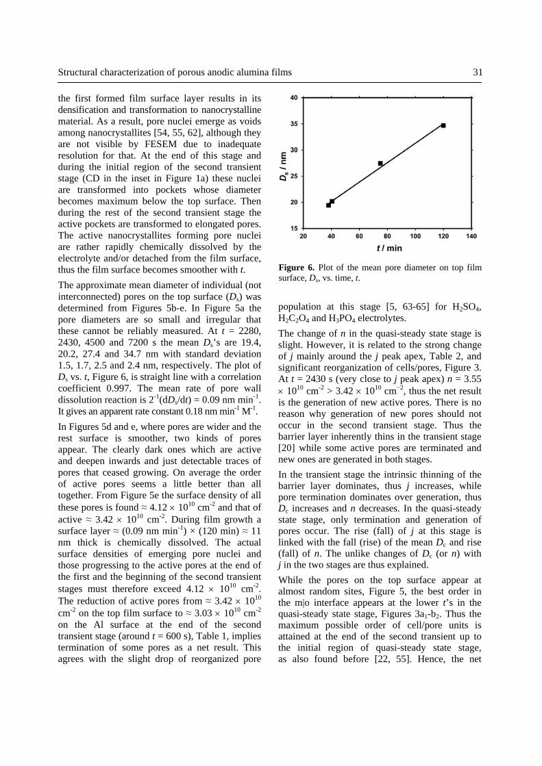
population at this stage [5, 63-65] for H2SO4, H2C2O4 and H3PO4 electrolytes. The change of n in the quasi-steady state stage is slight. However, it is related to the strong change of j mainly around the j peak apex, Table 2, and significant reorganization of cells/pores, Figure 3. At t = 2430 s (very close to j peak apex) n = 3.55 × 1010 cm-2 > 3.42 × 1010 cm−2, thus the net result is the generation of new active pores. There is no reason why generation of new pores should not occur in the second transient stage. Thus the barrier layer inherently thins in the transient stage [20] while some active pores are terminated and new ones are generated in both stages. In the transient stage the intrinsic thinning of the barrier layer dominates, thus j increases, while pore termination dominates over generation, thus Dc increases and n decreases. In the quasi-steady state stage, only termination and generation of pores occur. The rise (fall) of j at this stage is linked with the fall (rise) of the mean Dc and rise (fall) of n. The unlike changes of Dc (or n) with j in the two stages are thus explained. While the pores on the top surface appear at almost random sites, Figure 5, the best order in the m|o interface appears at the lower t’s in the quasi-steady state stage, Figures 3a1-b2. Thus the maximum possible order of cell/pore units is attained at the end of the second transient up to the initial region of quasi-steady state stage,as also found before [22, 55]. Hence, the net
the first formed film surface layer results in its densification and transformation to nanocrystalline material. As a result, pore nuclei emerge as voids among nanocrystallites [54, 55, 62], although they are not visible by FESEM due to inadequate resolution for that. At the end of this stage and during the initial region of the second transient stage (CD in the inset in Figure 1a) these nuclei are transformed into pockets whose diameter becomes maximum below the top surface. Then during the rest of the second transient stage the active pockets are transformed to elongated pores. The active nanocrystallites forming pore nuclei are rather rapidly chemically dissolved by the electrolyte and/or detached from the film surface, thus the film surface becomes smoother with t. The approximate mean diameter of individual (not interconnected) pores on the top surface (Ds) was determined from Figures 5b-e. In Figure 5a the pore diameters are so small and irregular that these cannot be reliably measured. At t = 2280, 2430, 4500 and 7200 s the mean Ds’s are 19.4, 20.2, 27.4 and 34.7 nm with standard deviation 1.5, 1.7, 2.5 and 2.4 nm, respectively. The plot of Ds vs. t, Figure 6, is straight line with a correlation coefficient 0.997. The mean rate of pore wall dissolution reaction is 2-1(dDs/dt) = 0.09 nm min-1. It gives an apparent rate constant 0.18 nm min-1 M-1. In Figures 5d and e, where pores are wider and the rest surface is smoother, two kinds of pores appear. The clearly dark ones which are active and deepen inwards and just detectable traces of pores that ceased growing. On average the order of active pores seems a little better than all together. From Figure 5e the surface density of all these pores is found ≈ 4.12 × 1010 cm-2 and that of active ≈ 3.42 × 1010 cm-2. During film growth a surface layer ≈ (0.09 nm min-1) × (120 min) ≈ 11 nm thick is chemically dissolved. The actual surface densities of emerging pore nuclei and those progressing to the active pores at the end of the first and the beginning of the second transient stages must therefore exceed 4.12 × 1010 cm-2. The reduction of active pores from ≈ 3.42 × 1010 cm-2 on the top film surface to ≈ 3.03 × 1010 cm-2 on the Al surface at the end of the second transient stage (around t = 600 s), Table 1, implies termination of some pores as a net result. This agrees with the slight drop of reorganized pore
Structural characterization of porous anodic alumina films 31
Figure 6. Plot of the mean pore diameter on top film surface, Ds, vs. time, t.

32 G. Patermarakis & T. M. Triantis
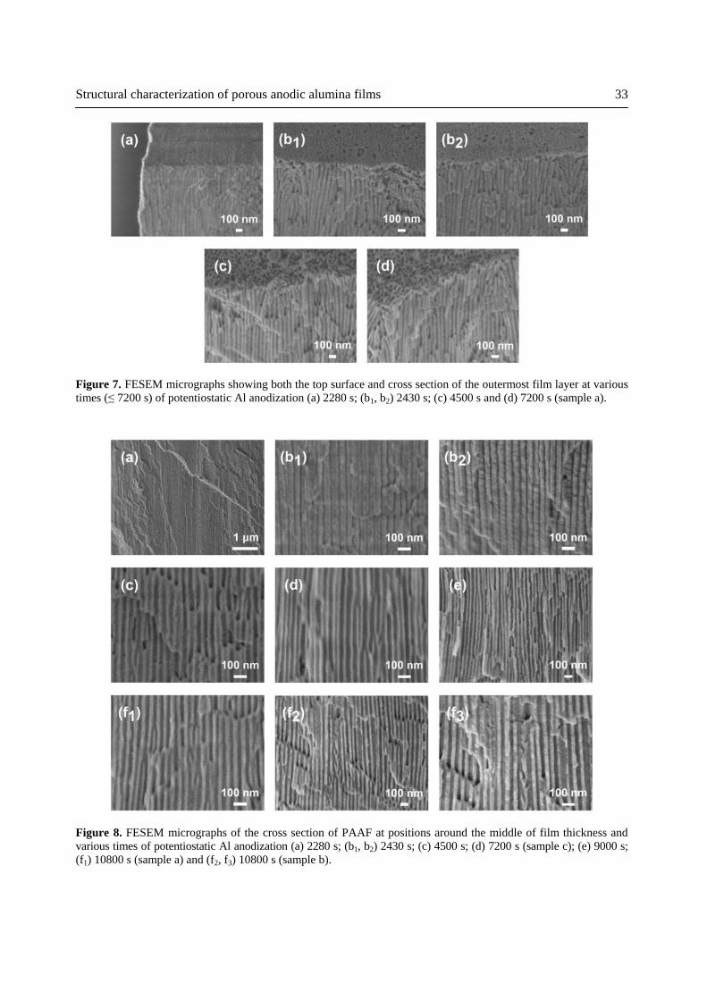
walls appear, coming from laterally generated pores directed inwards which are later terminated. The curved cell/pore units and their groups and the dendritic/serrated structures in the outer layer are thus linked with the termination of pores and generation of new ones from the bottom of some active pores, which thus branch inwards. At t’s ≤ 600 s such details are difficult to discern, that’s why related micrographs are not cited. The film broke mostly via intercellular surfaces, thus pores exhibited by cell fractures parallel to the pore axes were very rare and quite narrow, not providing adequate information. At t’s 4500 and 7200 s, Figures 7c and d, due to prolonged chemical attack of the pore walls in the outer layer, the pores are widened enough and details as the aforesaid become clearer. The above details in the outermost layer appear up to 7200 s. Up to this t, limiting thickness was nowhere established on the Al surface while the layer shown by the micrographs is much thinner than hf,a taken at the end of the second transient stage ≈ 7.9 μm, Table 1. This layer is formed up to a time in the initial region of the second transient stage, where the termination/generation rates of pockets or pores must be significant. FESEM images of fractures at positions ≈ hf,a/2 below the top surface appear in Figures 8a-f3. At t’s 2280 and 2430 s, Figures 8a-b2, almost all cell/pore units are straight. Key details as above are rare. Based on Table 1 data, these positions lie below the top surface by ≈ 16.1 and 23 μm, which fall in the range of hf,a among 7.9 and 32.2 μm taken at t’s 600 and 2280 s. The middle of PAAF section at 2280 and 2430 s thus corresponds to the region of barrier layer in films grown at t’s in the range 600-2280 s, where maximum self-ordering of pores appears. Thus, maximum ordering is associated with low and balanced rates of termination and generation of pores, which is reasonable. In Figure 8 for all other t’s 4500, 7200, 9000 and 10800 s, key details as above are clear, i.e. individual pores which stop growing and pores which branch inwards, while some branches of pores soon stop growing. At t = 10800 s Figures 8f1-f3 show fractures with excellent such details. Dendritic structures againappear with central trunks made of interpore walls
reduction of active pores on Al surface at the transient stage favours the self-ordering of cells/ pores. The drop of n and parallel progress of ordering after j peak apex confirm this too. Oppositely, the rise of n, e.g. from 2280 s up to j peak apex, degrades ordering. As shown in Figure 3 after 7200 s (sample b) the sequential slight worsening of order at 9000 s and improvement at 10800 s (sample a) relate with slight rise and then drop of n, again confirming the above. Thus, in general, the termination of pores improves and the generation degrades the self-ordering in both stages. At t = 9000 and 10800 s FESEM top surface images were also taken which were much different from those in Figure 5. Separate pores were not distinguished. Limiting thicknesses appear in the exfoliated and remaining surface areas (section 3.1). The outermost layer had a thorny/fibrous structure [66] consisting of elongated clusters of fibres made of tubules. Results are not presented, as exceeding the scope of this study.
3.5. FESEM study of PAAF cross sections; direct proof of pore termination/generation processes; formation of dendritic/serrated porous structures FESEM micrographs of the cross sections of PAAF at different t’s are shown in Figures 7-9. Micrographs in Figure 7 show locations in the cross sections just below and around the top film surface. Figure 8 shows locations at the middle of cross sections, thus at distance about hf,a/2 from the top surface, and Figure 9 shows the region around the barrier layer and just above. In Figure 7a at t = 2280 s the non-ordered porous structure on the top surface is again shown and concurrently the cross section surface shows that often the cell/pore units are not straight. Curved units and groups of curved units exist. At t = 2430 s, Figures 7b1 and b2, the non-ordered pores on the top surface are clear, mainly due to the widening of the pores by chemical attack of the pore walls. Also due to the higher magnification, the disordered structure in the outer layer with curved cell/pore units and their groups is clearer. Key details appear that are distinct pores that stop growing and pores branching inwards. Some branches soon stop growing. To the right edge of Figure 7b2 dendritic or serrated structures of pore
Structural characterization of porous anodic alumina films 33
Figure 8. FESEM micrographs of the cross section of PAAF at positions around the middle of film thickness and various times of potentiostatic Al anodization (a) 2280 s; (b1, b2) 2430 s; (c) 4500 s; (d) 7200 s (sample c); (e) 9000 s; (f1) 10800 s (sample a) and (f2, f3) 10800 s (sample b).
Figure 7. FESEM micrographs showing both the top surface and cross section of the outermost film layer at various times (≤ 7200 s) of potentiostatic Al anodization (a) 2280 s; (b1, b2) 2430 s; (c) 4500 s and (d) 7200 s (sample a).

of two adjacent cells and short wall branches directed outwards, like one side or two sides’ serrated structures. These structures are created by terminating side short pores which are branches directed inwards stemming from one central or two adjacent central pores. Serrated structures were observed also earlier and generally ascribed to O2 gas evolution together with plastic deformation [38, 67-69]. Since Al was vertically arranged in bath solution, all serrated structures should appear only in a common side (left or right) of all interpore wall trunks from which they stem [39]. Also these trunks should be inclined relative to the direction vertical to the Al surface [39]. But this is not the case. Thus here the dendritic structures come from coexisting generation and termination of pores. The above key details and dendritic/serrated structures appear at all t’s ≥ 4500 s because the location at hf,a/2 corresponds to the region of barrier layer for t’s > 2280 s, Table 1, where the rates of pore termination/generation processes are significant. Indeed from Table 1 at t = 4500 and 7200 s hf,a/2 is ≈ 71.7 and 91.8 μm, respectively, verifying the above. At t = 9000 and 10800 s (specimens a and b) the middle of remaining hf,a corresponds to the region of barrier layer when the produced thickness was ≈ (produced thickness calculated in section 3.1 - hf,a/2) = 120.3, 184.5 and 159.1 μm. Table 1 and Figure 2a show that these thicknesses appear at t’s in the range 2800-7200 s where Dc varies appreciably, Figure 4, and n alike does, Table 2, thus the rates of pore termination/generation processes are significant. Merging of pores inwards, thus their branching outwards, was not detected in any FESEM
micrograph. Pores ending and pores branching inwards observed in Figures 7 and 8 verify that the termination and generation of pores indeed occur in both the second transient and quasi-steady state stages. As previously said their rates are minimum and balanced in the first region of the last stage around the shallow j minimum, Table 1 and Figures 1a-c. Outside this region they alter appreciably the n, Dc and self-ordering degree as shown in Table 2, Figure 3 and section 3.4. Figures 7 and 8 show that the pores widen and their walls become thinner with t up to 9000 s. At 10800 s the pores become narrower and walls thicker compared with 9000 s. The hf,a’s in Table 1 show that the t interval of contact of the walls at position ≈ hf,a/2 above Al with electrolyte rises up to 9000 s and then falls at 10800 s justifying this behaviour. Representative FESEM images of the cross-section of innermost film layer in Figure 9 clearly show the columnar cellular structure of oxide and the hemispherical or hemispheroid barrier layer. The cells are detached from adjacent ones almost exclusively via intercellular boundary surfaces where the material is rarer [54]; thus it has less mechanical strength. The mean pore base diameter and the thicknesses of barrier layer and pore walls above it could be found from sections of cells crossing this layer via planes containing pore axes. However, the cells prefer to break vertically (rather than parallel) to axes and be detached via intercellular elongated surfaces. Due to the existence of barrier layer at the end of each cell with thickness comparable to that of the nearest pore walls and to the negligible thinning of these walls by chemical attack, each cell
34 G. Patermarakis & T. M. Triantis
Figure 9. FESEM micrographs of the cross section of the innermost film layer at various times of potentiostatic Al anodization (a) 2430 s; (b) 4500 s and (c) 9000 s.

thickness 2−1(Dc − Db) and the mean field strength in it (Ebl) is ΔP[2−1(Dc − Db)]−1. Other possible effects on Ebl such as those of the exact geometry of the barrier layer, dielectric behaviour of oxide, space charges possibly developed near m|o and o|e interfaces, contaminants and their contribution to ionic current, etc., were ignored without damaging the validity of analysis. Their inclusion would greatly complicate it without providing a novel and important conclusion for the subject. Also, for ease, uniform film growth is assumed along the Al surface. Electrochemical kinetic equations predict that j, tnan and tnca depend mostly on Ebl and the real temperature around the barrier layer region during anodising (Tan) [48], where Tan slightly exceeds T. When Ebl increases, j and tnan increase and tnca dcereases. When Tan (or T) rises then tnan falls and tnca rises while j can increase or decrease. Previous results [54, 71], as well as ja and tnan,a in Table 1, verify these predictions. Hence the change of j during anodising is followed by a similar change of tnan. At constant ΔP (or Pan) their change is explained by the change of Ebl and thus of 2−1(Dc − Db), Db, Dc and n on Al surface. It was earlier shown [48] that
tnan = 1 - (Db/Dc)2
Thereafter tnca = (Db/Dc)2 which also coincides with film porosity at pore bases (p) [53].
For constant Dc when tnan falls then Db rises, Eq. 1. This explains recent results [38, 39] for modulated pores taken by sequential anodization of pre-textured surfaces at various electrolytes. While interpore spacing and order were identical, the pore diameter increased and concurrently the j decreased. As j falls the tnan, which depends almost solely on j and Tan and negligibly on electrolyte kind [54, 71], also falls. Because Dc is constant then Db necessarily rises. At given anodization conditions, when j and thus tnan increases, Eq. 1 predicts decrease of porosity, explaining earlier results [72]. Several properties of PAAF and related anodization conditions are alike explained, predicted and designed by Eq. 1. For example, the protection against corrosion and resistance to friction of anodized Al materials become more efficient when the p and the rate of
exhibits highest mechanical strength around pore base. Sections via planes containing pore axes are thus rare or inexistent, Figure 9. These also justify the noted similar behaviour of thin films at t’s ≤ 600 s. 4. DISCUSSION In the sublayer of the barrier layer adjacent to the m|o interface, consisting of almost pure oxide [9, 70], under the high field, O2- and Al3+ solely migrate with transport numbers tnan and tnca, respectively, (tnan + tnca = 1). In the next sublayer up to the o|e interface, which is contaminated with small amounts of electrolyte anions, OH−, H+ and H2O [1, 2, 9, 56, 70] present at varying concentrations across the barrier layer and pore walls, the latter ionic species can also contribute to a small extent to the ionic current [54]. The O2− and Al3+ transport numbers thereto may differ slightly from the above. During PAAF growth, Al3+ ions are formed (Al → Al3+ + 3e-) at the m|o interface in close accordance with Faraday’s law [54]. Oxide is formed only at this interface at a rate equal to (6F)−1jSgtnan mol s−1 by a tnan portion of Al3+ ions which reacts with O2− ions that migrate and reach the m|o interface. The tnca = 1 − tnan portion of Al3+ ions migrate through the barrier layer and reach the o|e interface. If its outer sublayer were also pure oxide, thus migrating Al3+ would not react with contaminant species, this part of Al3+ would be ejected at rate (3F)−1jSgtnca mol s−1 to the pores filling solution where these Al3+ are solvated and complexated [57, 58]. In this case tnan coincides with oxide formation efficiency. Actually a small part of migrating Al3+ ions, varying from negligible or low enough (e.g. for anodization in oxalic, phosphoric and chromic acid electrolytes) up to a higher one (e.g. sulphuric acid), may be combined with contaminating species in this sublayer and form aluminium salt and/or hydroxides and/or oxyhydroxides [9, 70]. Then the material formation efficiency slightly exceeds this tnan. But always the contribution of contaminant species to charge transfer is trivial compared with that of Al3+ and O2− [54]. The following reasonable admittances are made. The barrier layer is hemispherical thus it has
Structural characterization of porous anodic alumina films 35
(1)

solutions, etc. Combinations of such conditions, which exclude burning, predict proper regimes of hard anodization. Eq. 1 can be transformed to Eqs. 2 and 3 Eq. 4 gives Dint/ΔP ≈ Dint/Pan = (2/1.05Ebl)[1 − (1 − tnan)1/2]−1, which can properly justify the Dint/Pan ≈ 2.5 nm V−1 values. Here best order is met in the initial region of the quasi-steady state stage at t’s 600-2280 s where Dint/Pan = 2.62-2.61 nm V−1. At 25 °C and j’s comparable to 26.7-43.3 mA cm−2, data [54, 71] show that tnan is relatively high and varies slightly around 0.77. This value of tnan and the above equation give Ebl = 1.464 V nm−1. Earlier [22] at ca = 1.53 M, T = 25 °C and j = 15 mA cm−2, with ΔV and Pan well outside the best ordering regime, Ebl was found ≈ 1.22 V nm−1. Since here at the same T value, jf’s are in the range of 26.7-43.3 mA cm−2 thus higher enough than 15 mA cm−2, Ebl values close to 1.464 V nm−1 are justified. At this T considering that Ebl varies slightly at various conditions of best order and around them, this must also occur for tnan. Then [1 − (1 − tnan)1/2]−1 also varies slightly. Hence, (2/1.05Ebl)[1 − (1 − tnan)1/2]−1 remains almost constant. As an example, for Dint/Pan = 2.5 nm V−1 and Ebl varying in a relatively wide range 1.264-1.664 V nm−1 (that includes 1.464 V nm−1 for best order), tnan lies in the not wide range 0.842-0.706. Since at conditions of best order and adjacent ones the Ebl and tnan values usually fall in ranges much narrower than the above, then Dint/Pan indeed varies only slightly. This behaviour implies that indeed a window of optimum Ebl exists where the order may become best. Eq. 4 and this window of Ebl justify the Dint/Pan values found here, a little above 2.5 nm V−1 for best order and ≈ 2.5 V nm−1 for adjacent order degree. The rates of pore termination/generation processes are also major factors affecting the order of pores.
pore wall dissolution are low. High tnan (thus low p) is attained at low T’s and/or high Ebl’s (thus j’s or Pan’s). Low dissolution rate is attained at low T’s and ca’s, by specific additives in electrolyte
Eqs. 2-4 also explain the present results. Eq. 4 predicts that at constant ΔP or Pan the Ebl (thus also j and tnan) rise during anodization only if 2−1(Dc − Db) falls. Eqs. 2 and 3 also show that when tnan rises and 2−1(Dc − Db) falls, then Db and Dc necessarily decrease, thus n increases. This is exactly shown by the results in Table 2 and Figure 4. If j varies in the quasi-steady state stage, an inevitable variation of n is predicted, thus termination of pores and generation of others occur, even at this stage. Experimental results indeed showed termination of existing and generation of new pores, Figures 3, 7 and 8. Each process dominates over the other within separate t region and at each t their combined effect defines the mean 2−1(Dc – Db), Dc and Db. It’s worth noting that Eqs. 1-3 link the 2−1(Dc − Db), Dc and Db with tnan without involving other parameters. Since Dc varies generally slightly, 2−1(Dc − Db) and Db must alike do. The employed method determines Dc effectively and accurately. Values of 2−1(Dc − Db) and Db can be alike calculated by these equations and tnan. The change of n with t is obviously related to the change of pore order. Results in section 3.1 showed that Pan and ΔV are not the exclusive factors controlling the order. The range of jf from 26.7 to 43.3 mA cm−2, at t’s 600-2280 s, Table 2, where the order is best, Figure 3, defines a specific Ebl (or 2−1(Dc – Db)) window, Eq. 4, which seems important. But at t’s 4500 and 7200 s the order is inferior while jf’s 42.3 and 32.4-32.7 mA cm−2 fall in the above jf range. Thus, in addition to Ebl, other factors are also important.
36 G. Patermarakis & T. M. Triantis
2-1(Dc - Db) = 2-1[1 - (1 - tnan)1/2]Dc or 1.05Dint = Dc = 2-1(Dc - Db)2[1 - (1 - tnan)1/2]-1
Db = 2-1(Dc - Db)2[1 - (1 - tnan)1/2]-1(1-tnan)1/2
Hence,
Ebl = ΔP[2-1(Dc - Db)]-1 = 2ΔP[1 - (1 - tnan)1/2]-1Dc-1 = 2ΔP[1 - (1 - tnan)1/2]-1(1 - tnan)1/2Db
-1, (ΔP ≈ Pan)
(2)
(3)
(4)

such as mean cell width, interpore spacing and surface density of pores in both the second transient and quasi-steady state stages. In the transient stage the cell width and interpore spacing increase and the surface density of pores decreases with current density. In the quasi-steady state stage the changes of these parameters with current density are the reverse of the above. Pores that stopped growing, pores branching inwards and dendritic/serrated ones were also revealed. The interpore spacing changes slightly around 2.5 nm V−1. 3. Major processes that regulate the change of film structural parameters near the barrier layer are the incessant termination/generation of pores in both stages along with the continuous inherent thinning of the barrier layer in the transient stage. Self-ordering improves when termination rate exceeds generation one. Order becomes best when these rates are minimum and balanced and the field strength in this layer falls in a specific window. These occur around the shallow minimum of current density in the initial region of the quasi-steady state stage. 4. The incessant termination and generation of pores, and thus the change of structural parameters and field strength, justify both the lack of stable perfect self-organised hexagonal order in sufficiently large areas or the entire Al surface and the destruction at prolonged anodization of high ordering observed in the initial region of the quasi-steady state stage. 5. The change of geometrical structural parameters of PAAF during potentiostatic anodization is directly opposite to the generally accepted trend of their linear changes with anodic potential or anodization voltage. This issue needs further detailed examination. 6. The present results and related analysis reveal novel key aspects of PAAF growth kinetics and mechanism and structure transformation, vital for Al anodization science and technology as well as numerous PAAF applications. ACKNOWLEDGMENT T. T. acknowledges NCSR “Demokritos”, Institute of Nanoscience and Nanotechnology for partial support of this work.
Dominance of termination rate improves it and that of generation degrades it in both the second transient and quasi-steady state stages. Best order appears in the first region of the last stage around the shallow j minimum where these rates are least and balanced and Ebl falls within the aforesaid window. The order degree is thus co-determined mostly by the (absolute and relative) rates of pore termination/generation processes. These incessant processes and the associated change of Ebl finally prevent perfect order in large enough areas, Figure 3. For potentiostatic anodization the results show that in the quasi-steady state stage the main processes defining Ebl and j are the termination and generation of pores. But in the second transient stage, while these processes are also active, the major process raising Ebl and j is the intrinsic thinning of mean barrier layer [20]. Determination of Db and 2−1(Dc − Db) in the present PAAF from FESEM images of cross sections formed by bending PAAF is unfeasible, Figure 9; only Dc may be thus tolerably determined. The best or only way to find reliable mean Db and 2−1(Dc − Db) values is via the mean Dc from film imprint on Al, tnan and Eqs. 1-3. At given Pan the change of Dc, Db and 2−1(Dc − Db) with t opposites a generally accepted trend of their linear changes with Pan or ΔV [4, 20, 22, 72-75]. Queries arise for their general validity, requiring further investigation. 5. CONCLUSIONS Based on the experimental results and related analysis in this work, the following main conclusions are derived: 1. During prolonged potentiostatic anodization of Al at the employed conditions the current density presents extremes. The anodization voltage alike varies around 25 V best ordering regime. Concurrently, other determinable parameters such as film mass and thickness also increase at rates strongly variable with time. 2. A detailed FESEM study of the m|o interface, top film surface, and cross section revealed, among other, changes in the pore ordering as well as in other basic structural parameters of PAAFs
Structural characterization of porous anodic alumina films 37

19. Pan, H., Lin, J., Feng, Y. and Gao, H. 2004, IEEE Trans. Nanotechnol., 3(4), 462.
20. O'Sullivan, J. P. and Wood, G. C. 1970, Proc. Roy. Soc. Ser. A Math Phys. Sci., 317(1731), 511.
21. Keller, F., Hunter, M. S. and Robinson, D. L. 1953, J. Electrochem. Soc., 100(9), 411.
22. Patermarakis, G. and Moussoutzanis, K. 2011, J. Electroanal. Chem., 659(2), 176.
23. Brace, A. W. 1992, Anodic Coating Defects: Their Causes and Cure, Technicopy Books, Stonehouse, Glos, England.
24. Brace, A. W. 2000, The technology of anodizing aluminium, Interall S.r.l.,, Modena, Italy.
25. Martin, C. R. 1996, Chem. Mater., 8(8), 1739.
26. Kovtyukhova, N. I. and Mallouk, T. E. 2005, Adv. Mater., 17(2), 187.
27. Ganley, J. C., Riechmann, K. L., Seebauer, E. G. and Masel, R. I. 2004, J. Catal., 227(1), 26.
28. Pellin, M. J., Stair, P. C., Xiong, G., Elam, J. W., Birrell, J., Curtiss, L., George, S. M., Han, C. Y., Iton, L., Kung, H., Kung, M. and Wang, H. H. 2005, Catal. Lett., 102(3-4), 127.
29. Burgos, N., Paulis, M. and Montes, M. 2003, J. Mater. Chem., 13(6), 1458.
30. Das, G., Patra, N., Gopalakrishnan, A., Zaccaria, R. P., Toma, A., Thorat, S., Di Fabrizio, E., Diaspro, A. and Salerno, M. 2012, Analyst, 137(8), 1785.
31. Toccafondi, C., La Rocca, R., Scarpellini, A., Salerno, M., Das, G. and Dante, S. 2015, Appl. Surf. Sci., 351, 738.
32. Napolskii, K. S., Roslyakov, I. V., Eliseev, A. A., Petukhov, A. V., Byelov, D. V., Grigoryeva, N. A., Bouwman, W. G., Lukashin, A. V., Kvashnina, K. O., Chumakov, A. P. and Grigoriev, S. V. 2010, J. Appl. Crystallog., 43(3), 531.
33. Zhu, X., Song, Y., Yu, D., Zhang, C. and Yao, W. 2013, Electrochem. Commun., 29, 71.
34. Masuda, H. and Fukuda, K. 1995, Science, 268(5216), 1466.
35. Zaraska, L., Kurowska, E., Sulka, G. D., Senyk, I. and Jaskula, M. 2014, J. Solid State Electrochem., 18(2), 361.
CONFLICT OF INTEREST STATEMENT The authors declare no conflict of interest. REFERENCES 1. Diggle, J. W., Downie, T. C. and Goulding,
C. W. 1969, Chem. Rev., 69(3), 365. 2. Young, L. 1961, Anodic Oxide Films,
Academic Press, London. 3. Sheasby, P. G. and Pinner, R. 2001, The
Surface Treatment and Finishing of Aluminum and Its Alloys, ASM International & Finishing Publications Ltd., USA-UK.
4. Sulka, G. D. 2008, Nanostructured Materials in Electrochemistry, A. Eftekhari (Ed.), John Wiley and Sons, Wienheim, 1.
5. Lee, W. and Park, S. J. 2014, Chem. Rev., 114(15), 7487.
6. Surganov, V. F. and Gorokh, G. G. 1993, Mater. Lett., 17(3-4), 121.
7. Surganov, V., Jansson, C., Nielsen, J. G., Morgen, P., Gorokh, G. and Larsen, A. N. 1988, Electrochim. Acta, 33(4), 517.
8. Dell'Oca, C. J. and Fleming, P. J. 1976, J. Electrochem. Soc., 123(10), 1487.
9. Parkhutik, V. P. 1986, Corros. Sci., 26(4), 295. 10. Parkhutik, V. P. and Shershulsky, V. I.
1992, J. Phys. D, 25(8), 1258. 11. Patermarakis, G., Chandrinos, J. and
Masavetas, K. 2007, J. Solid State Electrochem., 11(9), 1191.
12. Jessensky, O., Muller, F. and Gosele, U. 1998, Appl. Phys. Lett., 72(10), 1173.
13. Zhang, L., Cho, H. S., Li, F., Metzger, R. M. and Doyle, W. D. 1998, J. Mater. Sci. Lett., 17(4), 291.
14. Jessensky, O., Muller, F. and Gosele, U. 1998, J. Electrochem. Soc., 145(11), 3735.
15. Nielsch, K., Choi, J., Schwirn, K., Wehrspohn, R. B. and Gösele, U. 2002, Nano Lett., 2(7), 677.
16. Li, A. P., Muller, F., Bimer, A., Nielsch, K. and Gosele, U. 1998, J. Appl. Phys., 84(11), 6023.
17. Li, A. P., Müller, F. and Gösele, U. 2000, Electrochem. Solid-State Lett., 3(3), 131.
18. Masuda, H., Yotsuya, M., Asano, M., Nishio, K., Nakao, M., Yokoo, A. and Tamamura, T. 2001, Appl. Phys. Lett., 78(6), 826.
38 G. Patermarakis & T. M. Triantis

57. Vogel, A. I. 1976, Macro and Semimicro Quantitative Analysis, Longman, London.
58. Alexeyev, V. N. 1980, Qualitative Chemical Analysis, Mir Publishers, Moscow.
59. Patermarakis, G. and Moussoutzanis, K. 2002, J. Solid State Electrochem., 6(7), 475.
60. Ruiquan, Y., Longfei, J., Xufei, Z., Ye, S., Dongliang, Y. and Aijun, H. 2012, RSC Adv., 2(32), 12474.
61. Belca, I., Kasalica, B., Zekovic, L., Jovanic, B. and Vasilic, R. 1999, Electrochim. Acta, 45(6), 993.
62. Patermarakis, G., Karayianni, H., Masavetas, K. and Chandrinos, J. 2009, J. Solid State Electrochem., 13(12), 1831.
63. Li, F., Zhang, L. and Metzger, R. M. 1998, Chem. Mater., 10(9), 2470.
64. Sulka, G. D., Stroobants, S., Moshchalkov, V., Borghs, G. and Celis, J. P. 2002, J. Electrochem. Soc., 149(7), D97.
65. Zaraska, L., Sulka, G. D. and Jaskuła, M. 2010, Surf. Coat. Technol., 204(11), 1729.
66. Kikuchi, T., Nishinaga, O., Nakajima, D., Kawashima, J., Natsui, S., Sakaguchi, N. and Suzuki, R. O. 2014, Scientific Reports, 4, 7411.
67. Zhu, X., Liu, L., Song, Y., Jia, H., Yu, H., Xiao, X. and Yang, X. 2008, Monatsh. Chem., 139(9), 999.
68. Li, D., Jiang, C., Jiang, J. and Lu, J. G. 2009, Chem. Mater., 21(2), 253.
69. Li, D., Zhao, L., Jiang, C. and Lu, J. G. 2010, Nano Lett., 10(8), 2766.
70. Thompson, G. E., Furneaux, R. C. and Wood, G. C. 1978, Corros. Sci., 18(5), 481.
71. Patermarakis, G. and Moussoutzanis, K. 2009, Electrochim. Acta, 54(9), 2434.
72. Vega, V., García, J., Montero-Moreno, J. M., Hernando, B., Bachmann, J., Prida, V. M. and Nielsch, K. 2015, ACS Appl. Mater. Interfaces, 7(51), 28682.
73. Montero-Moreno, J. M., Sarret, M. and Müller, C. 2010, Microporous Mesoporous Mater., 136(1-3), 68.
74. Sulka, G. D. and Parkoła, K. G. 2007, Electrochim. Acta, 52(5), 1880.
75. Ebihara, K., Takahashi, H. and Nagayama, M. 1982, J. Met. Finish. Soc. Jpn., 33(4), 156.
36. Qin, X., Zhang, J., Meng, X., Deng, C., Zhang, L., Ding, G., Zeng, H. and Xu, X. 2015, Appl. Surf. Sci., 328, 459.
37. Ma, Y., Wen, Y., Li, J., Li, Y., Zhang, Z., Feng, C. and Sun, R. 2016, Scientific Reports, 6, 39165.
38. Zaraska, L., Jaskuła, M. and Sulka, G. D. 2016, Mater. Lett., 171, 315.
39. Zaraska, L., Brudzisz, A., Wierzbicka, E. and Sulka, G. D. 2016, Electrochim. Acta, 198, 259.
40. Lee, K. H. and Wong, C. C. 2009, J. Appl. Phys., 106(10).
41. Han, X. Y. and Shen, W. Z. 2011, J. Electroanal. Chem., 655(1), 56.
42. Chen, B., Lu, K. and Tian, Z. 2011, Electrochim. Acta, 56(27), 9802.
43. Masuda, H., Yamada, H., Satoh, M., Asoh, H., Nakao, M. and Tamamura, T. 1997, Appl. Phys. Lett., 71(19), 2770.
44. Lee, W., Ji, R., Gösele, U. and Nielsch, K. 2006, Nat. Mater., 5(9), 741.
45. Kwon, N., Kim, K., Heo, J. and Chung, I. 2009, J. Vac. Sci. Technol. A Vac. Surf. Films, 27(4), 803.
46. Patermarakis, G. 2014, J. Electroanal. Chem., 730, 69.
47. Patermarakis, G. and Kapiris, G. 2013, J. Solid State Electrochem., 17(4), 1133.
48. Patermarakis, G. and Plytas, J. 2016, J. Electroanal. Chem., 769, 97.
49. Dobos, D. 1975, Electrochemical Data: A Handbook for Electrochemists in Industry and Universities, Elsevier.
50. Masuda, H., Hasegwa, F. and Ono, S. 1997, J. Electrochem. Soc., 144(5), L127.
51. Pashchanka, M. and Schneider, J. J. 2011, J. Mater. Chem., 21(46), 18761.
52. Stepniowski, W. J., Forbot, D., Norek, M., Michalska-Domańska, M. and Król, A. 2014, Electrochim. Acta, 133, 57.
53. Mirzoev, R. A., Davydov, A. D., Vystupov, S. I. and Kabanova, T. B. 2019, Electrochim. Acta, 294, 276.
54. Patermarakis, G. and Diakonikolaou, J. 2012, J. Solid State Electrochem., 16(9), 2921.
55. Patermarakis, G. 2009, J. Electroanal. Chem., 635(1), 39.
56. Patermarakis, G., Lenas, P., Karavassilis, C. and Papayiannis, G. 1991, Electrochim. Acta, 36(3-4), 709.
Structural characterization of porous anodic alumina films 39