tps92830evm user's guide - texas instruments (useful for stop or tail light and daytime running...
TRANSCRIPT

1SLVUB41–July 2017Submit Documentation Feedback
Copyright © 2017, Texas Instruments Incorporated
TPS92830-Q1 EVM User's Guide
User's GuideSLVUB41–July 2017
TPS92830-Q1 EVM User's Guide
The TPS92830-Q1 evaluation module (EVM) helps designers evaluate the operation and performance ofthe TPS92830-Q1 device, a linear LED controller with external N-channel MOSFETs for automotivelighting applications.
Contents1 Introduction ................................................................................................................... 2
1.1 Features of TPS92830EVM KIT .................................................................................. 21.2 Typical Applications ................................................................................................ 21.3 TPS92830EVM KIT Description .................................................................................. 2
2 Test Setup .................................................................................................................... 73 Board Layout ................................................................................................................. 84 Schematic and Bill of Materials........................................................................................... 10
4.1 Schematics ......................................................................................................... 104.2 Bill of Materials .................................................................................................... 11
List of Figures
1 TPS92830EVM Board....................................................................................................... 32 LED Board .................................................................................................................... 53 TPS92830EVM Setup....................................................................................................... 74 TPS92830EVM Board Layout.............................................................................................. 85 LED Board Layout ........................................................................................................... 96 TPS92830EVM Board Schematic........................................................................................ 107 LED Board Schematic ..................................................................................................... 11
List of Tables
1 Jumper J3..................................................................................................................... 42 Jumper J4..................................................................................................................... 43 Jumper J7..................................................................................................................... 44 Jumper J12 ................................................................................................................... 65 Jumper J6..................................................................................................................... 66 LED String Short-to-GND Jumper ......................................................................................... 67 LED String-Open Jumper................................................................................................... 68 Shorted-LED Jumper........................................................................................................ 69 ICTRL Jumper................................................................................................................ 710 TPS92830EVM Parameters ................................................................................................ 711 TPS92830EVM Board BOM .............................................................................................. 1112 LED Board BOM............................................................................................................ 14
TrademarksAll trademarks are the property of their respective owners.

Introduction www.ti.com
2 SLVUB41–July 2017Submit Documentation Feedback
Copyright © 2017, Texas Instruments Incorporated
TPS92830-Q1 EVM User's Guide
1 Introduction
1.1 Features of TPS92830EVM KIT• Channel-Current Setting by Separate High-Side Sensing Resistors• LED-Short and -Open Protection and Fault Reporting• Auto-Recovery After Removing Fault State• One-Fails–All-Fail With Fault Floating or Only-Failed-Channel-Off LED Failure Mode With Fault Pulled
Up• Stand-Alone Operation With Full Duty Cycle or PWM Dimming via TPS92830-Q1 Internal PWM
Generator (Useful for Stop or Tail Light and Daytime Running Light (DRL) or Position LightApplications)
• PWM Duty Cycle and Frequency Configurable via Jumper• PWM Output Optional for Sync Dimming (PWMOUT Must Be Pulled Up to 5 V Through a Resistor)• Analog Dimming With Potentiometer on LED Board (Can Be Used for Bin Resistor)• Optional LED Board Thermal Protection via ICTRL• Current Derating During Overvoltage• Open-Fault Detection Mask During Dropout Mode• Compatible With Different Type N-Channel MOSFETs
1.2 Typical ApplicationsAutomotive DRL, position light, stop or tail light, turn indicator, reverse light, fog light, and so forth.
1.3 TPS92830EVM KIT Description
The TPS92830EVM KIT includes two boards: TPS92830EVM board and LED board. This sectiondescribes the connectors and jumpers of the two boards.
www.ti.com Introduction
3SLVUB41–July 2017Submit Documentation Feedback
Copyright © 2017, Texas Instruments Incorporated
TPS92830-Q1 EVM User's Guide
1.3.1 TPS92830EVM Board
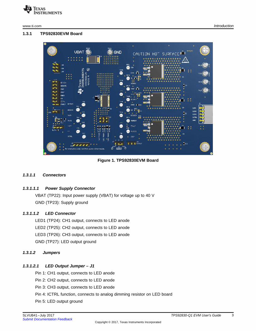
Figure 1. TPS92830EVM Board
1.3.1.1 Connectors
1.3.1.1.1 Power Supply ConnectorVBAT (TP22): Input power supply (VBAT) for voltage up to 40 V
GND (TP23): Supply ground
1.3.1.1.2 LED ConnectorLED1 (TP24): CH1 output, connects to LED anode
LED2 (TP25): CH2 output, connects to LED anode
LED3 (TP26): CH3 output, connects to LED anode
GND (TP27): LED output ground
1.3.1.2 Jumpers
1.3.1.2.1 LED Output Jumper – J1Pin 1: CH1 output, connects to LED anode
Pin 2: CH2 output, connects to LED anode
Pin 3: CH3 output, connects to LED anode
Pin 4: ICTRL function, connects to analog dimming resistor on LED board
Pin 5: LED output ground
Introduction www.ti.com
4 SLVUB41–July 2017Submit Documentation Feedback
Copyright © 2017, Texas Instruments Incorporated
TPS92830-Q1 EVM User's Guide
1.3.1.2.2 5V LDO Input Jumper – J2Allows VIN to connect to a 5-V LDO
1.3.1.2.3 Control Signal Input Jumper – J3
Table 1. Jumper J3
Label Jumper J3 With Shunt Without ShuntDIAGEN Pins 1–2 Connect to VIN via a resistor divider Use external control signalDERATE Pins 3–4 Connect to VIN via a resistor divider Use external control signalPWM1 Pins 5–6 Connect to VIN via a resistor divider Use external control signalPWM2 Pins 7–8 Connect to VIN via a resistor divider Use external control signalPWM3 Pins 9–10 Connect to VIN via a resistor divider Use external control signal
FD Pins 11–12 Connect to VIN via a resistor divider Use external control signalICTRL Pins 13–14 Connect to off-board bin resistor Use external control signal or leave floatingFAULT Pins 15–16 Pull up to 5 V Use external control signal or leave floating
1.3.1.2.4 PWM Generator Configuration Jumper – J4To use the TPS92830-Q1 internal PWM dimming function, there are two requirements.• Keep the FD pin at a low level and remove the shunt on J3 pins 11–12.• Keep all PWM inputs at a high level by keeping the shunts on J3 pins 5–6, pins 7–8 and pins 9–10.
Table 2. Jumper J4
Label
Jumper J4With Shunt – 1
Without Shunt – 0 Description
Pins 1–2 Pins 3–4 Pins 5–6200 Hz, 5% 1 0 0 PWM generator outputs 200 Hz, 5% duty-cycle PWM400 Hz, 20% 0 1 0 PWM generator outputs 400 Hz, 20% duty-cycle PWM
200 Hz, 80% 0 0 1PWM generator outputs 200 Hz, 80% duty-cycle PWMNote: Put a shunt on J7 pins 1–2 to realize 80% dutycycle.
1.3.1.2.5 PWMOUT Jumper – J7
Table 3. Jumper J7
LabelWith Shunt – 1
Without Shunt – 0 DescriptionPins 1–2 Pins 2–3
RC 1 0 For 200 Hz, 80% PWM configuration, combine with shunt on J4 pins5–6
5 V 0 1 For PWMOUT pullup under 200 Hz, 5% or 400 Hz, 20%

www.ti.com Introduction
5SLVUB41–July 2017Submit Documentation Feedback
Copyright © 2017, Texas Instruments Incorporated
TPS92830-Q1 EVM User's Guide
1.3.1.3 Test PointsAll the pins on the TPS92830-Q1 device except CP1N, CP1P, CP2N, and CP2P have test points on theEVM, which helps users to observe the waveform on the pins.
1.3.2 LED Board
Figure 2. LED Board
1.3.2.1 ConnectorsLED1 (TP1): Positive input of LED board, connects to LED1 on TPS92830EVM
LED2 (TP2): Positive input of LED board, connects to LED2 on TPS92830EVM
LED3 (TP3): Positive input of LED board, connects to LED3 on TPS92830EVM
GND (TP4): LED output ground, connects to GND on TPS92830EVM
1.3.2.2 Jumpers
1.3.2.2.1 LED Outputs – J12
Introduction www.ti.com
6 SLVUB41–July 2017Submit Documentation Feedback
Copyright © 2017, Texas Instruments Incorporated
TPS92830-Q1 EVM User's Guide
Table 4. Jumper J12
Label Jumper J12 DescriptionLED1 Pin 5 Positive input of LED board, connects to LED1 on TPS92830EVM boardLED2 Pin 4 Positive input of LED board, connects to LED2 on TPS92830EVM boardLED3 Pin 3 Positive input of LED board, connects to LED3 on TPS92830EVM boardICTRL Pin 2 Analog dimming function, connects to ICTRL on TPS92830EVM boardGND Pin 1 LED output ground, connects to GND on TPS92830EVM board
1.3.2.2.2 LED Anode Jumper – J6
Table 5. Jumper J6
Label Jumper J6 With Shunt Without ShuntLED1 Pins 1–2 Connect LED1 connector to LED string Disconnect LED1 connector from LED stringLED2 Pins 3–4 Connect LED2 connector to LED string Disconnect LED2 connector from LED stringLED3 Pins 5–6 Connect LED3 connector to LED string Disconnect LED3 connector from LED string
1.3.2.2.3 LED String Short-to-GND Jumper
Table 6. LED String Short-to-GND Jumper
Label Jumper With Shunt Without ShuntLED1 SH GND J1 LED1 string short to GND Normal operationLED2 SH GND J7 LED2 string short to GND Normal operationLED3 SH GND J13 LED3 string short to GND Normal operation
1.3.2.2.4 LED String-Open Jumpers
Table 7. LED String-Open Jumper
Label Jumper With Shunt Without Shunt— J5 Normal operation LED1 string open— J11 Normal operation LED2 string open— J17 Normal operation LED3 string open
1.3.2.2.5 Shorted-LED Jumper
Table 8. Shorted-LED Jumper
Label Jumper With Shunt Without ShuntSH D1 J2 Short D1 Normal operationSH D2 J3 Short D2 Normal operationSH D3 J4 Short D3 Normal operationSH D4 J8 Short D4 Normal operationSH D5 J9 Short D5 Normal operationSH D6 J10 Short D6 Normal operationSH D7 J14 Short D7 Normal operationSH D8 J15 Short D8 Normal operationSH D9 J16 Short D9 Normal operation
TPS92830EVM Board LED Board
DC Power Supply
VBAT GND
www.ti.com Test Setup
7SLVUB41–July 2017Submit Documentation Feedback
Copyright © 2017, Texas Instruments Incorporated
TPS92830-Q1 EVM User's Guide
1.3.2.2.6 ICTRL Jumper
Table 9. ICTRL Jumper
Label Jumper With Shunt – 1Without Shunt – 0 Description
Analog dimming J18 1 0 Connect ICTRL to a potentiometer for analog dimming
Thermal protection J19 0 1 Connect ICTRL to an NTC resistor for overtemperatureprotection
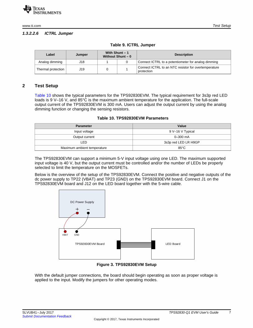
2 Test Setup
Table 10 shows the typical parameters for the TPS92830EVM. The typical requirement for 3s3p red LEDloads is 9 V–16 V, and 85°C is the maximum ambient temperature for the application. The full-scaleoutput current of the TPS92830EVM is 300 mA. Users can adjust the output current by using the analogdimming function or changing the sensing resistors.
Table 10. TPS92830EVM Parameters
Parameter ValueInput voltage 9 V–16 V Typical
Output current 0–300 mALED 3s3p red LED LR H9GP
Maximum ambient temperature 85°C
The TPS92830EVM can support a minimum 5-V input voltage using one LED. The maximum supportedinput voltage is 40 V, but the output current must be controlled and/or the number of LEDs be properlyselected to limit the temperature on the MOSFETs.
Below is the overview of the setup of the TPS92830EVM. Connect the positive and negative outputs of thedc power supply to TP22 (VBAT) and TP23 (GND) on the TPS92830EVM board. Connect J1 on theTPS92830EVM board and J12 on the LED board together with the 5-wire cable.
Figure 3. TPS92830EVM Setup
With the default jumper connections, the board should begin operating as soon as proper voltage isapplied to the input. Modify the jumpers for other operating modes.
Board Layout www.ti.com
8 SLVUB41–July 2017Submit Documentation Feedback
Copyright © 2017, Texas Instruments Incorporated
TPS92830-Q1 EVM User's Guide
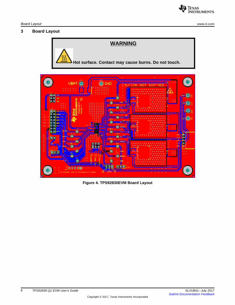
3 Board Layout
WARNING
Hot surface. Contact may cause burns. Do not touch.
Figure 4. TPS92830EVM Board Layout

www.ti.com Board Layout
9SLVUB41–July 2017Submit Documentation Feedback
Copyright © 2017, Texas Instruments Incorporated
TPS92830-Q1 EVM User's Guide
Figure 5. LED Board Layout
Q3
BU
K763R
8-8
0E
,118
GN
D
D1
SL44-E
3/5
7T
VIN
VIN
VIN
2.2
µF
C1
GN
D
GN
D
DE
RA
TE
DIA
GE
N_X
DE
RA
TE
_X
PW
M3_X
DIA
GE
N
PW
M1
PW
M2
PW
M3
FD
ICT
RL
PW
MO
UT
/FA
ULT
PW
MC
HG
IRE
F
DIA
GE
N_X
DE
RA
TE
_X
FD
_X
ICT
RL_X
/FA
ULT
_X
DIA
GE
ND
ER
AT
EP
WM
1P
WM
2P
WM
3F
DIC
TR
L/F
AU
LT
GN
D
GN
D
GN
D
VIN
1
NC
2G
ND
3
GN
D4
VO
UT
5
U2
TP
S7B
6950Q
DB
VR
Q1
J2
VIN
4.7
µF
C12
GN
DG
ND
5V
GN
D
2200pF
C2
DN
P
GN
D
2200pF
C7
DN
P
GN
D
2200pF
C11
DN
P
SE
NS
E3
ISN
3G
3
SE
NS
E2
G2
ISN
2
SE
NS
E1
G1
ISN
1
ISP
CP
1N
CP
1P
CP
2P
CP
2N
CP
OU
T
GN
D
VB
AT
GN
D
5V
VIN
0.1
5µ
FC
10
FD
_X
/FA
ULT
_X
8.0
6k
R8
LE
D1
VIN
1.0
0k
R17
CP
1P
1
CP
1N
2
GN
D3
CP
2N
4
CP
2P
5
CP
OU
T6
IN7
DIA
GE
N8
DE
RA
TE
9
PW
M1
10
PW
M2
11
PW
M3
12
FD
13
ICT
RL
14
IRE
F15
PW
MC
HG
16
FA
ULT
17
PW
MO
UT
18
SE
NS
E3
19
G3
20
ISN
321
SE
NS
E2
22
G2
23
ISN
224
SE
NS
E1
25
G1
26
ISN
127
ISP
28
U1
TP
S92830Q
PW
RQ
1
LE
D2
LE
D3
12
34
56
78
910
11
12
13
14
15
16
J3
0.0
68
µF
C14
0.1
2µ
FC
15
1.4
0k
R18
28.0
kR
27
110k
R26
GN
DG
ND
200
Hz
5%
400
Hz
20%
200
Hz
80%
PW
MC
HG
DIA
GE
N>
9V
DE
RE
AT
E>
18V
PW
MIN
>6V
FD
>6V
12
34
56
J4
130k
R11
20.0
kR
20
20.0
kR
21
20.0
kR
24
20.0
kR
25
GN
DG
ND
180k
R12
DIA
GE
ND
ER
AT
EF
D
PW
M1_X
PW
M2_X
PW
M3_X
PW
M1_X
20.0
kR
22
GN
D
PW
M2_X
20.0
kR
23
GN
D
PW
M1
PW
M2
PW
M3
Q1
BU
K763R
8-8
0E
,118
Q2
BU
K763R
8-8
0E
,118
0R2
0R7
0R10
10nF
C3
GN
D0
R3
0R
5
0R
6
1.0
0R
1
1.0
0R
4
1.0
0R
9
1.2
µF
C16
ICT
RL_X
5
4
1
2
3
J8
GN
D
1
2
3
J9
5V
12
34
56
J5
VIN
2.2
µF
C4
0.0
1µ
FC
5
GN
D
541 2 3
J1
10nF
C9
GN
D
10nF
C13
GN
D
TP
2T
P1
TP
3
TP
4T
P5
TP
6
TP
7T
P8
TP
9
TP
10
TP
12
TP
11
TP
13
TP
14
TP
15
TP
16
TP
17
TP
18
TP
19
TP
20
TP
21
DIA
GE
ND
ER
AT
EP
WM
1
G3
SE
NS
E3
PW
MO
UT
/FA
ULT
PW
MC
HG
IRE
FIC
TR
L
FD
PW
M3
PW
M2
ISN
3S
EN
SE
2
G2
ISN
2S
EN
SE
1
G1
ISN
1IS
P
VB
AT
GN
DT
P22
TP
23
LE
D1
LE
D2
TP
24
TP
25
LE
D3
GN
DT
P26
TP
27 1
2
3
J6
10.0
kR
19
1
2
3
J7
PW
MO
UT
5V
PW
MO
UT
For
200
Hz
80%
duty
cycle
, putshuton
J4
pin
s5
−6,and
J7
pin
s1
−2
For
PW
MO
UT
pull
up
under
200 H
z 5
%, 400
Hz
20%
, put
shuton
J7
pin
s 2
−3
Put charg
epum
pcapacitors
C6,
C8,C
10
as c
lose
toT
PS
92830-Q
1as
possib
le
DIA
GE
Nactive
when
VIN
> 9
VD
ER
AT
E a
ctive
when
VIN
>18V
PW
M a
ctive w
hen
VIN
>6V
FD
active w
hen
VIN
>6V
VIN
0.0
1µ
FC
6
0.0
1µ
FC
8
4700pF
C18
DN
P
4700pF
C19
DN
P
4700pF
C17
DN
P
9-1
6V
78.7
kR
13
78.7
kR
14
78.7
kR
15
78.7
kR
16
Schematic and Bill of Materials www.ti.com
10 SLVUB41–July 2017Submit Documentation Feedback
Copyright © 2017, Texas Instruments Incorporated
TPS92830-Q1 EVM User's Guide
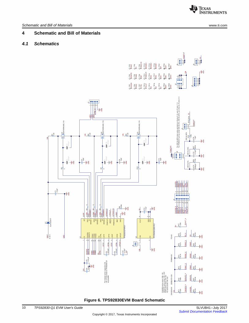
4 Schematic and Bill of Materials
4.1 Schematics
Figure 6. TPS92830EVM Board Schematic
GND
GND
GND
J5
J3
J9J8
J2
J10
J4
J11
J17
J16J15J14
LED1 LED2
TP1 TP2
LED3 GND
TP3 TP4
GND
LED1
LED2
LED3
1 2
3 4
5 6
J6
J1
GND
J7
GND
J13
GND
10K
R1
ICTRL
GND
ICTRL
J18 J19
5
4
1
2
3
J12
3
1 2
Red
D1
LR H9GP-HZKX-1-1-Z
3
1 2
Red
D2
LR H9GP-HZKX-1-1-Z
3
1 2
Red
D3
LR H9GP-HZKX-1-1-Z
3
1 2
Red
D4
LR H9GP-HZKX-1-1-Z
3
1 2
Red
D5
LR H9GP-HZKX-1-1-Z
3
1 2
Red
D6
LR H9GP-HZKX-1-1-Z
3
1 2
Red
D7
LR H9GP-HZKX-1-1-Z
3
1 2
Red
D8
LR H9GP-HZKX-1-1-Z
3
1 2
Red
D9
LR H9GP-HZKX-1-1-Z
0
R2
47.0k ohm
t° RT1
www.ti.com Schematic and Bill of Materials
11SLVUB41–July 2017Submit Documentation Feedback
Copyright © 2017, Texas Instruments Incorporated
TPS92830-Q1 EVM User's Guide
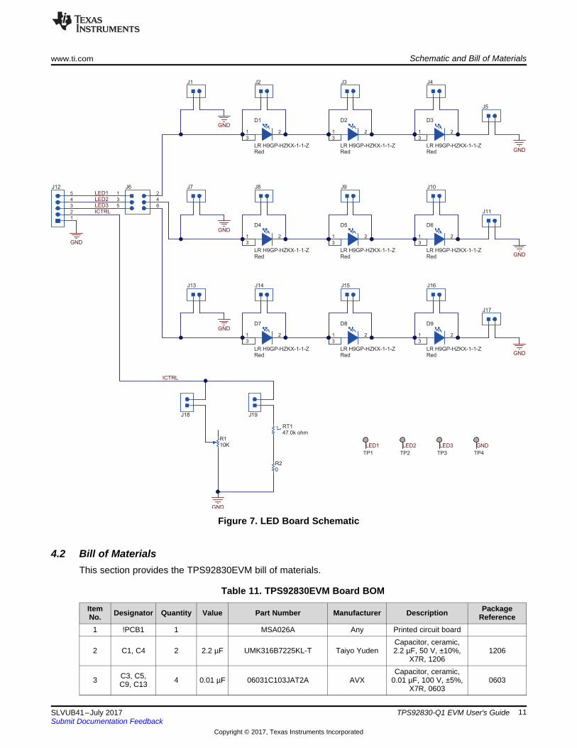
Figure 7. LED Board Schematic
4.2 Bill of MaterialsThis section provides the TPS92830EVM bill of materials.
Table 11. TPS92830EVM Board BOM
ItemNo. Designator Quantity Value Part Number Manufacturer Description Package
Reference1 !PCB1 1 MSA026A Any Printed circuit board
2 C1, C4 2 2.2 µF UMK316B7225KL-T Taiyo YudenCapacitor, ceramic,2.2 µF, 50 V, ±10%,
X7R, 12061206
3 C3, C5,C9, C13 4 0.01 µF 06031C103JAT2A AVX
Capacitor, ceramic,0.01 µF, 100 V, ±5%,
X7R, 06030603

Schematic and Bill of Materials www.ti.com
12 SLVUB41–July 2017Submit Documentation Feedback
Copyright © 2017, Texas Instruments Incorporated
TPS92830-Q1 EVM User's Guide
Table 11. TPS92830EVM Board BOM (continued)ItemNo. Designator Quantity Value Part Number Manufacturer Description Package
Reference
4 C6, C8 2 0.01 µF GCM155R71H103KA55D MuRataCapacitor, ceramic,
0.01 µF, 50 V, ±10%,C0G/NP0, 0402
0402
5 C10 1 0.15 µF C0805C154K5RACTU KemetCapacitor, ceramic,
0.15 µF, 50 V, ±10%,X7R, 0805
0805
6 C12 1 4.7 µF 0603ZD475KAT2A AVXCapacitor, ceramic,4.7 µF, 10 V, ±10%,
X5R, 06030603
7 C14 1 0.068µF CGA3E3X7S2A683K080AB TDK
Capacitor, ceramic,0.068 µF, 100 V,±10%, X7S, AEC-
Q200 Grade 1, 0603
0603
8 C15 1 0.12 µF GRM188R61A124KA01D MuRataCapacitor, ceramic,
0.12 µF, 10 V, ±10%,X5R, 0603
0603
9 C16 1 1.2 µF C0805C125K8RACTU KemetCapacitor, ceramic,1.2 µF, 10 V, ±10%,
X7R, 08050805
10 D1 1 40 V SL44-E3/57T Vishay-Semiconductor
Diode, Schottky, 40 V,4 A, SMC SMC
11 H1, H2,H3, H4 4 NY PMS 440 0025 PH B&F Fastener
Supply
Machine screw,round, 4-40 × 1/4,nylon, Philips pan
head
Screw
12 H5, H6,H7, H8 4 1902C Keystone Standoff, hex, 0.5 in
L, 4-40, nylon Standoff
13 J1 1 IPL1-105-01-L-S-RA-K SamtecHeader (shrouded),2.54 mm, 5x1, gold,
R/A, TH
Header(Shrouded),
2.54 mm, 5×1,R/A, TH
14 J2 1 TSW-102-07-G-S Samtec Header, 100 mil, 2×1,gold, TH 2×1 header
15 J3 1 TSW-108-07-G-D Samtec Header, 100 mil, 8×2,gold, TH 8×2 header
16 J4, J5 2 TSW-103-07-G-D Samtec Header, 100 mil, 8×2,gold, TH 3×2 header
17 J6, J7, J9 3 TSW-103-07-G-S Samtec Header, 100 mil, 3×1,gold, TH 3×1 header
18 J8 1 TSW-105-07-G-S Samtec Header, 100 mil, 5×1,gold, TH 5×1 header
19 Q1, Q2, Q3 3 80 V BUK763R8-80E,118 NXPSemiconductor
MOSFET, N-CH, 80V, 120 A, AEC-Q101,
DDPAKDDPAK
20 R1, R4, R9 3 1 Ω CRCW12061R00FKEA Vishay-Dale Resistor, 1, 1%, 0.25W, 1206 1206
21R2, R3,R5, R6,R7, R10
6 0 CRCW06030000Z0EA Vishay-Dale RES, 0, 5%, 0.1 W,0603 0603
22 R8 1 8.06kΩ RT0603BRD078K06L Yageo America Resistor, 8.06 kΩ,
0.1%, 0.1 W, 0603 0603
23 R11 1 130 kΩ CRCW0603130KFKEA Vishay-Dale Resistor, 130 kΩ, 1%,0.1 W, 0603 0603
24 R12 1 180 kΩ CRCW0603180KJNEA Vishay-Dale Resistor, 180 kΩ, 5%,0.1 W, 0603 0603
25 R13, R14,R15, R16 4 78.7
kΩ RC0603FR-0778K7L Yageo America Resistor, 78.7 kΩ,1%, 0.1 W, 0603 0603

www.ti.com Schematic and Bill of Materials
13SLVUB41–July 2017Submit Documentation Feedback
Copyright © 2017, Texas Instruments Incorporated
TPS92830-Q1 EVM User's Guide
Table 11. TPS92830EVM Board BOM (continued)ItemNo. Designator Quantity Value Part Number Manufacturer Description Package
Reference
26 R17 1 1 kΩ CRCW06031K00FKEA Vishay-Dale Resistor, 1 kΩ, 1%,0.1 W, 0603 0603
27 R18 1 1.4 kΩ CRCW06031K40FKEA Vishay-Dale Resistor, 1.4 kΩ, 1%,0.1 W, 0603 0603
28 R19 1 10 kΩ CRCW060310K0FKEA Vishay-Dale Resistor, 10 kΩ, 1%,0.1 W, 0603 0603
29R20, R21,R22, R23,R24, R25
6 20 kΩ CRCW060320K0FKEA Vishay-Dale Resistor, 20 kΩ, 1%,0.1 W, 0603 0603
30 R26 1 110 kΩ CRCW0603110KFKEA Vishay-Dale Resistor, 110 kΩ, 1%,0.1 W, 0603 0603
31 R27 1 28 kΩ CRCW060328K0FKEA Vishay-Dale Resistor, 28 kΩ, 1%,0.1 W, 0603 0603
32
SH-J1, SH-J2, SH-J3,SH-J4, SH-J5, SH-J6,SH-J7, SH-J8, SH-J9,
SH-J10
10 1x2 969102-0000-DA 3M Shunt, 100 mil, goldplated, black Shunt
33
TP1, TP2,TP3, TP4,TP5, TP6,
TP7,TP8, TP9,
TP10,TP11,TP12,TP13,TP14,TP15,TP16,TP17,TP18,TP19,TP20,TP21
21 5002 Keystone Test point, miniature,white, TH
White miniaturetest point
34
TP22,TP23,TP24,TP25,TP26,TP27
6 1502-2 Keystone Terminal, turret, TH,double
Keystone1502-2
35 U1 1 TPS92830QPWRQ1 TexasInstruments
3-ch high-currentlinear LED controllerwith diagnostics andone-fails-all-fail fault
bus, PW0028A
PW0028A
36 U2 1 TPS7B6950QDBVRQ1 TexasInstruments
High-voltage ultralowIq low-dropout
regulator, DBV0005ADBV0005A
37 C2, C7,C11 0 2200
pF GRM188R72A222KA01D MuRataCapacitor, ceramic,
2200 pF, 100 V,±10%, X7R, 0603
0603
38 C17, C18,C19 0 4700
pF GRM188R71E472KA01D MuRataCapacitor, ceramic,
4700 pF, 25 V, ±10%,X7R, 0603
0603
39FID1, FID2FID3, FID4FID5, FID6
0 N/A N/AFiducial mark.
There is nothing tobuy or mount.
Fiducial
Schematic and Bill of Materials www.ti.com
14 SLVUB41–July 2017Submit Documentation Feedback
Copyright © 2017, Texas Instruments Incorporated
TPS92830-Q1 EVM User's Guide
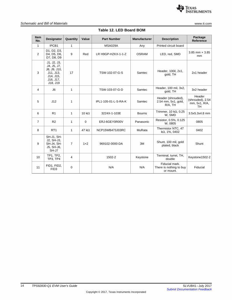
Table 12. LED Board BOM
ItemNo. Designator Quantity Value Part Number Manufacturer Description Package
Reference1 !PCB1 1 MSA029A Any Printed circuit board
2D1, D2, D3,D4, D5, D6,D7, D8, D9
9 Red LR H9GP-HZKX-1-1-Z OSRAM LED, red, SMD 3.85 mm × 3.85mm
3
J1, J2, J3,J4, J5, J7,J8, J9, J10,J11, J13,J14, J15,J16, J17,J18, J19
17 TSW-102-07-G-S Samtec Header, 100il, 2x1,gold, TH 2x1 header
4 J6 1 TSW-103-07-G-D Samtec Header, 100 mil, 3x2,gold, TH 3x2 header
5 J12 1 IPL1-105-01-L-S-RA-K SamtecHeader (shrouded),2.54 mm, 5x1, gold,
R/A, TH
Header(shrouded), 2.54mm, 5x1, R/A,
TH
6 R1 1 10 kΩ 3224X-1-103E Bourns Trimmer, 10 kΩ, 0.25W, SMD 3.5x5.3x4.8 mm
7 R2 1 0 ERJ-6GEY0R00V Panasonic Resistor, 0.5%, 0.125W, 0805 0805
8 RT1 1 47 kΩ NCP15WB473J03RC MuRata Thermistor NTC, 47kΩ, 1%, 0402 0402
9
SH-J1, SH-J2, SH-J3,SH-J4, SH-J5, SH-J6,
SH-J7
7 1×2 969102-0000-DA 3M Shunt, 100 mil, goldplated, black Shunt
10 TP1, TP2,TP3, TP4 4 1502-2 Keystone Terminal, turret, TH,
double Keystone1502-2
11 FID1, FID2,FID3 0 N/A N/A
Fiducial mark.There is nothing to buy
or mount.Fiducial

IMPORTANT NOTICE FOR TI DESIGN INFORMATION AND RESOURCES
Texas Instruments Incorporated (‘TI”) technical, application or other design advice, services or information, including, but not limited to,reference designs and materials relating to evaluation modules, (collectively, “TI Resources”) are intended to assist designers who aredeveloping applications that incorporate TI products; by downloading, accessing or using any particular TI Resource in any way, you(individually or, if you are acting on behalf of a company, your company) agree to use it solely for this purpose and subject to the terms ofthis Notice.TI’s provision of TI Resources does not expand or otherwise alter TI’s applicable published warranties or warranty disclaimers for TIproducts, and no additional obligations or liabilities arise from TI providing such TI Resources. TI reserves the right to make corrections,enhancements, improvements and other changes to its TI Resources.You understand and agree that you remain responsible for using your independent analysis, evaluation and judgment in designing yourapplications and that you have full and exclusive responsibility to assure the safety of your applications and compliance of your applications(and of all TI products used in or for your applications) with all applicable regulations, laws and other applicable requirements. Yourepresent that, with respect to your applications, you have all the necessary expertise to create and implement safeguards that (1)anticipate dangerous consequences of failures, (2) monitor failures and their consequences, and (3) lessen the likelihood of failures thatmight cause harm and take appropriate actions. You agree that prior to using or distributing any applications that include TI products, youwill thoroughly test such applications and the functionality of such TI products as used in such applications. TI has not conducted anytesting other than that specifically described in the published documentation for a particular TI Resource.You are authorized to use, copy and modify any individual TI Resource only in connection with the development of applications that includethe TI product(s) identified in such TI Resource. NO OTHER LICENSE, EXPRESS OR IMPLIED, BY ESTOPPEL OR OTHERWISE TOANY OTHER TI INTELLECTUAL PROPERTY RIGHT, AND NO LICENSE TO ANY TECHNOLOGY OR INTELLECTUAL PROPERTYRIGHT OF TI OR ANY THIRD PARTY IS GRANTED HEREIN, including but not limited to any patent right, copyright, mask work right, orother intellectual property right relating to any combination, machine, or process in which TI products or services are used. Informationregarding or referencing third-party products or services does not constitute a license to use such products or services, or a warranty orendorsement thereof. Use of TI Resources may require a license from a third party under the patents or other intellectual property of thethird party, or a license from TI under the patents or other intellectual property of TI.TI RESOURCES ARE PROVIDED “AS IS” AND WITH ALL FAULTS. TI DISCLAIMS ALL OTHER WARRANTIES ORREPRESENTATIONS, EXPRESS OR IMPLIED, REGARDING TI RESOURCES OR USE THEREOF, INCLUDING BUT NOT LIMITED TOACCURACY OR COMPLETENESS, TITLE, ANY EPIDEMIC FAILURE WARRANTY AND ANY IMPLIED WARRANTIES OFMERCHANTABILITY, FITNESS FOR A PARTICULAR PURPOSE, AND NON-INFRINGEMENT OF ANY THIRD PARTY INTELLECTUALPROPERTY RIGHTS.TI SHALL NOT BE LIABLE FOR AND SHALL NOT DEFEND OR INDEMNIFY YOU AGAINST ANY CLAIM, INCLUDING BUT NOTLIMITED TO ANY INFRINGEMENT CLAIM THAT RELATES TO OR IS BASED ON ANY COMBINATION OF PRODUCTS EVEN IFDESCRIBED IN TI RESOURCES OR OTHERWISE. IN NO EVENT SHALL TI BE LIABLE FOR ANY ACTUAL, DIRECT, SPECIAL,COLLATERAL, INDIRECT, PUNITIVE, INCIDENTAL, CONSEQUENTIAL OR EXEMPLARY DAMAGES IN CONNECTION WITH ORARISING OUT OF TI RESOURCES OR USE THEREOF, AND REGARDLESS OF WHETHER TI HAS BEEN ADVISED OF THEPOSSIBILITY OF SUCH DAMAGES.You agree to fully indemnify TI and its representatives against any damages, costs, losses, and/or liabilities arising out of your non-compliance with the terms and provisions of this Notice.This Notice applies to TI Resources. Additional terms apply to the use and purchase of certain types of materials, TI products and services.These include; without limitation, TI’s standard terms for semiconductor products http://www.ti.com/sc/docs/stdterms.htm), evaluationmodules, and samples (http://www.ti.com/sc/docs/sampterms.htm).
Mailing Address: Texas Instruments, Post Office Box 655303, Dallas, Texas 75265Copyright © 2017, Texas Instruments Incorporated