tps6514x triple output lcd supply with linear regulator
TRANSCRIPT

VI
2.7 V to 5.8 VBoost
Converter
NegativeCharge Pump
PositiveCharge Pump
Power Good
Linear RegulatorController
VO1
Up to 15 V / 400 mA
VO2
Down to ±12 V / 20 mA
VO3
Up to 30 V / 20 mA
VO4
3.3 V
PG
TPS6514x
Copyright © 2016, Texas Instruments Incorporated
Product
Folder
Sample &Buy
Technical
Documents
Tools &
Software
Support &Community
ReferenceDesign
An IMPORTANT NOTICE at the end of this data sheet addresses availability, warranty, changes, use in safety-critical applications,intellectual property matters and other important disclaimers. PRODUCTION DATA.
TPS65140, TPS65141, TPS65145SLVS497F –SEPTEMBER 2003–REVISED JUNE 2016
TPS6514x Triple Output LCD Supply With Linear Regulator and Power Good
1
1 Features1• 2.7-V to 5.8-V Input Voltage Range• 1.6-MHz Fixed Switching Frequency• 3 Independent Adjustable Outputs• Main Output up to 15 V With <1% Typical Output
Voltage Accuracy• Virtual Synchronous Converter Technology• Negative Regulated Charge Pump Driver VO2
• Positive Charge Pump Converter VO3
• Auxiliary 3.3-V Linear Regulator Controller• Internal Soft Start• Internal Power-On Sequencing• Fault Detection of All Outputs (TPS65140 and
TPS65145)• No Fault Detection (TPS65141)• Thermal Shutdown• System Power Good• Available in 24-Pin HTSSOP and 24-Pin VQFN
PowerPAD™ Packages
2 Applications• TFT LCD Displays for Notebooks• TFT LCD Displays for Monitors• Portable DVD Players• Tablet PCs• Car Navigation Systems• Industrial Displays
Block Diagram
3 DescriptionThe TPS6514x series offers a compact and smallpower supply solution to provide all three voltagesrequired by thin film transistor (TFT) LCD displays.The auxiliary linear regulator controller can be usedto generate a 3.3-V logic power rail for systemspowered by a 5-V supply rail only.
The main output VO1 is a 1.6-MHz fixed frequencyPWM boost converter providing the source drivevoltage for the LCD display. The device is available intwo versions with different internal switch currentlimits to allow the use of a smaller external inductorwhen lower output power is required. The TPS65140and TPS65141 has a typical switch current limit of2.3 A and the TPS65145 has a typical switch currentlimit of 1.37 A. A fully integrated adjustable chargepump doubler or tripler provides the positive LCDgate drive voltage. An externally adjustable negativecharge pump provides the negative gate drivevoltage. Due to the high 1.6-MHz switching frequencyof the charge pumps, inexpensive and small 220-nFcapacitors can be used.
Additionally, the TPS6514x series has a systempower good output to indicate when all supply railsare acceptable. For LCD panels powered by 5 V thedevice has a linear regulator controller using anexternal transistor to provide a regulated 3.3-V outputfor the digital circuits. For maximum safety, theTPS65140 and TPS65145 goes into shutdown assoon as one of the outputs is out of regulation. Thedevice can be enabled again by toggling the input orthe enable (EN) pin to GND. The TPS65141 does notenter shutdown when one of its outputs is below itspower good threshold.
Device Information(1)
PART NUMBER PACKAGE BODY SIZE (NOM)
TPS6514xHTSSOP (24) 7.80 mm × 4.40 mmVQFN (24) 4.00 mm × 4.00 mm
(1) For all available packages, see the orderable addendum atthe end of the data sheet.

2
TPS65140, TPS65141, TPS65145SLVS497F –SEPTEMBER 2003–REVISED JUNE 2016 www.ti.com
Product Folder Links: TPS65140 TPS65141 TPS65145
Submit Documentation Feedback Copyright © 2003–2016, Texas Instruments Incorporated
Table of Contents1 Features .................................................................. 12 Applications ........................................................... 13 Description ............................................................. 14 Revision History..................................................... 25 Pin Configuration and Functions ......................... 36 Specifications......................................................... 4
6.1 Absolute Maximum Ratings ...................................... 46.2 ESD Ratings.............................................................. 46.3 Recommended Operating Conditions....................... 46.4 Thermal Information .................................................. 56.5 Electrical Characteristics........................................... 56.6 Dissipation Ratings ................................................... 76.7 Typical Characteristics .............................................. 7
7 Detailed Description .............................................. 87.1 Overview ................................................................... 87.2 Functional Block Diagram ......................................... 97.3 Feature Description................................................. 107.4 Device Functional Modes........................................ 11
8 Application and Implementation ........................ 12
8.1 Application Information............................................ 128.2 Typical Application .................................................. 128.3 System Examples ................................................... 21
9 Power Supply Recommendations ...................... 2210 Layout................................................................... 23
10.1 Layout Guidelines ................................................. 2310.2 Layout Example .................................................... 2310.3 Thermal Considerations ........................................ 23
11 Device and Documentation Support ................. 2411.1 Device Support...................................................... 2411.2 Documentation Support ........................................ 2411.3 Related Links ........................................................ 2411.4 Receiving Notification of Documentation Updates 2411.5 Community Resources.......................................... 2411.6 Trademarks ........................................................... 2411.7 Electrostatic Discharge Caution............................ 2411.8 Glossary ................................................................ 25
12 Mechanical, Packaging, and OrderableInformation ........................................................... 25
4 Revision HistoryNOTE: Page numbers for previous revisions may differ from page numbers in the current version.
Changes from Revision E (November 2012) to Revision F Page
• Added ESD Ratings table, Thermal Information table, Feature Description section, Device Functional Modessection, Application and Implementation section, Power Supply Recommendations section, Layout section, Deviceand Documentation Support section, and Mechanical, Packaging, and Orderable Information section ............................... 1
• Deleted Ordering Information table; see POA at the end of the data sheet........................................................................... 1• Changed typical value of VREF to 1.213 V from 1.13 V .......................................................................................................... 5• Moved Figure 12 through Figure 23 from Typical Applications to Application Curves......................................................... 19

Not to scale
Thermal
Pad
1FB1 24 EN
2FB4 23 ENR
3BASE 22 COMP
4VIN 21 FB2
5SW 20 REF
6SW 19 GND
7PGND 18 DRV
8PGND 17 C1–
9SUP 16 C1+
10PG 15 C2–/MODE
11GND 14 C2+
12FB3 13 OUT3Not to scale
Thermal
Pad
24
FB
27
VIN
1COMP 18 C2–/MODE
23
RE
F8
SW
2ENR 17 C2+
22
GN
D9
SW
3EN 16 OUT3
21
DR
V10
PG
ND
4FB1 15 FB3
20
C1
–11
PG
ND
5FB4 14 GND
19
C1+
12
SU
P
6BASE 13 PG
3
TPS65140, TPS65141, TPS65145www.ti.com SLVS497F –SEPTEMBER 2003–REVISED JUNE 2016
Product Folder Links: TPS65140 TPS65141 TPS65145
Submit Documentation FeedbackCopyright © 2003–2016, Texas Instruments Incorporated
5 Pin Configuration and Functions
PWP Package24-Pin HTSSOP
Top ViewRGE Package24-Pin VQFN
Top View
Pin FunctionsPIN
I/O DESCRIPTIONNAME
NO.HTSSOP VQFN
BASE 3 6 O Base drive output for the external transistorC1+ 16 19 — Positive terminal of the charge pump flying capacitorC1– 17 20 — Negative terminal of the charge pump flying capacitor
C2+ 14 17 — Positive terminal for the charge pump flying capacitor. If the device runs in voltage doublermode, this pin must be left open.
C2–/MODE 15 18 —
Negative terminal of the charge pump flying capacitor and charge pump MODE pin. If theflying capacitor is connected to this pin, the converter operates in a voltage tripler mode. If thecharge pump must operate in a voltage doubler mode, the flying capacitor is removed and theC2-/MODE pin must be connected to GND.
COMP 22 1 — Compensation pin for the main boost converter. A small capacitor is connected to this pin.DRV 18 21 O External charge pump driver
EN 24 3 I Enable pin of the device. This pin must be terminated and not be left floating. A logic highenables the device and a logic low shuts down the device.
ENR 23 2 I Enable pin of the linear regulator controller. This pin must be terminated and not be leftfloating. Logic high enables the regulator and a logic low puts the regulator in shutdown.
FB1 1 4 I Feedback pin of the boost converterFB2 21 24 I Feedback pin of negative charge pumpFB3 12 15 I Feedback pin of positive charge pump
FB4 2 5 I Feedback pin of the linear regulator controller. The linear regulator controller is set to a fixedoutput voltage of 3.3 V or 3 V depending on the version.
GND 11, 19 14, 22 — GroundOUT3 13 16 O Positive charge pump output
PG 10 13 OOpen-drain output indicating when all outputs VO1, VO2, VO3 are within 10% of their nominaloutput voltage. The output goes low when one of the outputs falls below 10% of their nominaloutput voltage.
PGND 7, 8 10, 11 — Power groundPowerPAD /Thermal Die — — — The PowerPAD or exposed thermal die must be connected to power ground pins (PGND)
REF 20 23 O Internal reference output typically 1.23 V

4
TPS65140, TPS65141, TPS65145SLVS497F –SEPTEMBER 2003–REVISED JUNE 2016 www.ti.com
Product Folder Links: TPS65140 TPS65141 TPS65145
Submit Documentation Feedback Copyright © 2003–2016, Texas Instruments Incorporated
Pin Functions (continued)PIN
I/O DESCRIPTIONNAME
NO.HTSSOP VQFN
SUP 9 12 I
Supply pin of the positive, negative charge pump, boost converter, and gate drive circuit. Thispin must be connected to the output of the main boost converter and cannot be connected toany other voltage source. For performance reasons, TI does not recommend connecting abypass capacitor directly to this pin.
SW 5, 6 8, 9 I Switch pin of the boost converterVIN 4 7 I Input voltage pin of the device.
(1) Stresses beyond those listed under Absolute Maximum Ratings may cause permanent damage to the device. These are stress ratingsonly, which do not imply functional operation of the device at these or any other conditions beyond those indicated under RecommendedOperating Conditions. Exposure to absolute-maximum-rated conditions for extended periods may affect device reliability.
(2) All voltage values are with respect to network ground terminal.
6 Specifications
6.1 Absolute Maximum Ratingsover operating free-air temperature range (unless otherwise noted) (1)
MIN MAX UNITVoltages on pin VIN (2) –0.3 6 VVoltages on pin VO1, SUP, PG (2) –0.3 15.5 VVoltages on pin EN, MODE, ENR (2) –0.3 VI+ 0.3 VVoltage on pin SW (2) 20 VPower good maximum sink current (PG) 1 mAContinuous power dissipation See Dissipation RatingsLead temperature (soldering, 10 s) 260 °COperating junction temperature, TJ –40 150 °CStorage temperature, Tstg –65 150 °C
(1) JEDEC document JEP155 states that 500-V HBM allows safe manufacturing with a standard ESD control process.(2) JEDEC document JEP157 states that 250-V CDM allows safe manufacturing with a standard ESD control process.
6.2 ESD RatingsVALUE UNIT
V(ESD)Electrostaticdischarge
Human-body model (HBM), per ANSI/ESDA/JEDEC JS-001 (1) ±2000V
Charged-device model (CDM), per JEDEC specification JESD22-C101 (2) ±500
(1) See the application information section for further information.
6.3 Recommended Operating ConditionsMIN NOM MAX UNIT
VI Input voltage 2.7 5.8 VL Inductor (1) 4.7 µHTA Operating ambient temperature –40 85 °CTJ Operating junction temperature –40 125 °C

5
TPS65140, TPS65141, TPS65145www.ti.com SLVS497F –SEPTEMBER 2003–REVISED JUNE 2016
Product Folder Links: TPS65140 TPS65141 TPS65145
Submit Documentation FeedbackCopyright © 2003–2016, Texas Instruments Incorporated
(1) For more information about traditional and new thermal metrics, see the Semiconductor and IC Package Thermal Metrics applicationreport.
6.4 Thermal Information
THERMAL METRIC (1)TPS6514x
UNITPWP (HTSSOP) RGE (VQFN)24 PINS 24 PINS
RθJA Junction-to-ambient thermal resistance 37.2 34.2 °C/WRθJC(top) Junction-to-case (top) thermal resistance 18.9 35.5 °C/WRθJB Junction-to-board thermal resistance 16.4 11.7 °C/WψJT Junction-to-top characterization parameter 0.4 0.4 °C/WψJB Junction-to-board characterization parameter 16.2 11.7 °C/WRθJC(bot) Junction-to-case (bottom) thermal resistance 2.1 3.2 °C/W
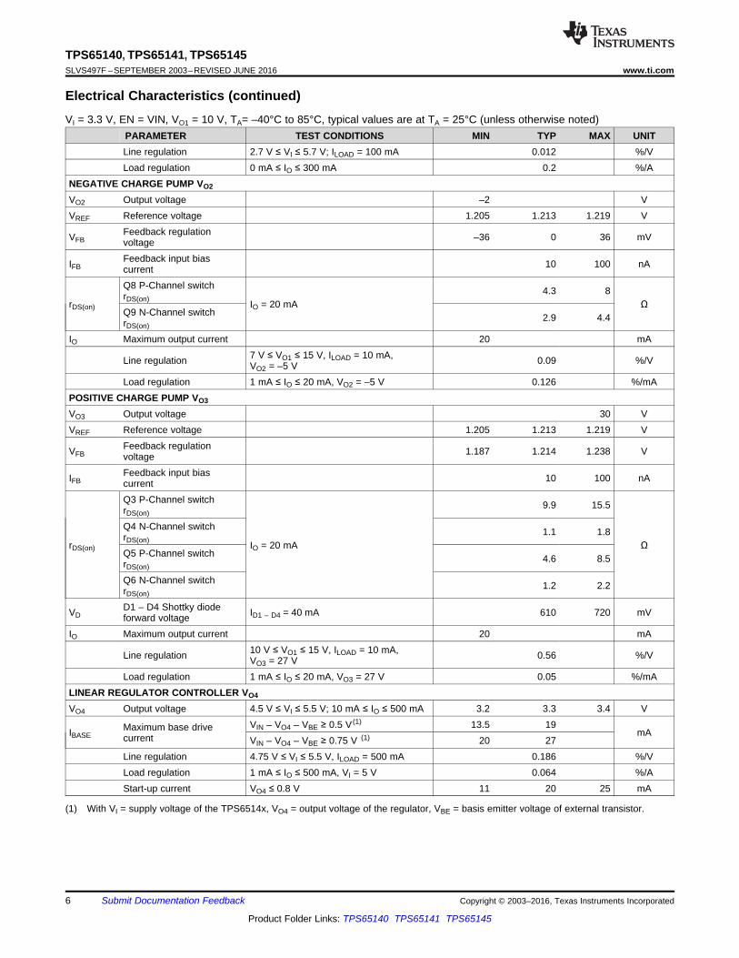
6.5 Electrical CharacteristicsVI = 3.3 V, EN = VIN, VO1 = 10 V, TA= –40°C to 85°C, typical values are at TA = 25°C (unless otherwise noted)
PARAMETER TEST CONDITIONS MIN TYP MAX UNITSUPPLY CURRENTVI Input voltage 2.7 5.5 V
IQ Quiescent current into VIN ENR = GND, VO3 = 2 × VO1,Boost converter not switching 0.7 0.9 mA
IQChargeCharge pump quiescentcurrent into SUP
VO1 = SUP = 10 V, VO3 = 2 × VO1 1.7 2.7mA
VO1 = SUP = 10 V, VO3 = 3 × VO1 3.9 6
IQENLDO controller quiescentcurrent into VIN ENR = VIN, EN = GND 300 800 μA
ISD Shutdown current into VIN EN = ENR = GND 1 10 μA
VUVLOUndervoltage lockoutthreshold VI falling 2.2 2.4 V
Thermal shutdown Temperature rising 160 °CLOGIC SIGNALS EN, ENRVIH High level input voltage 1.5 VVIL Low level input voltage 0.4 VII Input leakage current EN = GND or VIN 0.01 0.1 µAMAIN BOOST CONVERTERVO1 Output voltage 5 15 V
VO1 – VIN Minimum input to outputvoltage difference 1 V
VREF Reference voltage 1.205 1.213 1.219 V
VFBFeedback regulationvoltage 1.136 1.146 1.154 V
IFBFeedback input biascurrent 10 100 nA
rDS(on)N-MOSFET ON-resistance(Q1)
VO1 = 10 V, ISW = 500 mA 195 290mΩ
VO1 = 5 V, ISW = 500 mA 285 420
ILIMN-MOSFET switch currentlimit (Q1)
TPS65140, TPS65141 1.6 2.3 2.6 ATPS65145 0.96 1.37 1.56 A
rDS(on)P-MOSFET ON-resistance(Q2)
VO1 = 10 V, ISW = 100 mA 9 15Ω
VO1 = 5 V, ISW = 100 mA 14 22
IMAXMaximum P-MOSFET peakswitch current 1 A
ILEAK Switch leakage current VSW = 15 V 1 10 µA
fSW Oscillator frequency0°C ≤ TA ≤ 85°C 1.295 1.6 2.1
MHz–40°C ≤ TA ≤ 85°C 1.191 1.6 2.1
6
TPS65140, TPS65141, TPS65145SLVS497F –SEPTEMBER 2003–REVISED JUNE 2016 www.ti.com
Product Folder Links: TPS65140 TPS65141 TPS65145
Submit Documentation Feedback Copyright © 2003–2016, Texas Instruments Incorporated
Electrical Characteristics (continued)VI = 3.3 V, EN = VIN, VO1 = 10 V, TA= –40°C to 85°C, typical values are at TA = 25°C (unless otherwise noted)
PARAMETER TEST CONDITIONS MIN TYP MAX UNIT
(1) With VI = supply voltage of the TPS6514x, VO4 = output voltage of the regulator, VBE = basis emitter voltage of external transistor.
Line regulation 2.7 V ≤ VI ≤ 5.7 V; ILOAD = 100 mA 0.012 %/VLoad regulation 0 mA ≤ IO ≤ 300 mA 0.2 %/A
NEGATIVE CHARGE PUMP VO2
VO2 Output voltage –2 VVREF Reference voltage 1.205 1.213 1.219 V
VFBFeedback regulationvoltage –36 0 36 mV
IFBFeedback input biascurrent 10 100 nA
rDS(on)
Q8 P-Channel switchrDS(on) IO = 20 mA
4.3 8Ω
Q9 N-Channel switchrDS(on)
2.9 4.4
IO Maximum output current 20 mA
Line regulation 7 V ≤ VO1 ≤ 15 V, ILOAD = 10 mA,VO2 = –5 V 0.09 %/V
Load regulation 1 mA ≤ IO ≤ 20 mA, VO2 = –5 V 0.126 %/mAPOSITIVE CHARGE PUMP VO3
VO3 Output voltage 30 VVREF Reference voltage 1.205 1.213 1.219 V
VFBFeedback regulationvoltage 1.187 1.214 1.238 V
IFBFeedback input biascurrent 10 100 nA
rDS(on)
Q3 P-Channel switchrDS(on)
IO = 20 mA
9.9 15.5
Ω
Q4 N-Channel switchrDS(on)
1.1 1.8
Q5 P-Channel switchrDS(on)
4.6 8.5
Q6 N-Channel switchrDS(on)
1.2 2.2
VDD1 – D4 Shottky diodeforward voltage ID1 – D4 = 40 mA 610 720 mV
IO Maximum output current 20 mA
Line regulation 10 V ≤ VO1 ≤ 15 V, ILOAD = 10 mA,VO3 = 27 V 0.56 %/V
Load regulation 1 mA ≤ IO ≤ 20 mA, VO3 = 27 V 0.05 %/mALINEAR REGULATOR CONTROLLER VO4
VO4 Output voltage 4.5 V ≤ VI ≤ 5.5 V; 10 mA ≤ IO ≤ 500 mA 3.2 3.3 3.4 V
IBASEMaximum base drivecurrent
VIN – VO4 – VBE ≥ 0.5 V (1) 13.5 19mA
VIN – VO4 – VBE ≥ 0.75 V (1) 20 27Line regulation 4.75 V ≤ VI ≤ 5.5 V, ILOAD = 500 mA 0.186 %/VLoad regulation 1 mA ≤ IO ≤ 500 mA, VI = 5 V 0.064 %/AStart-up current VO4 ≤ 0.8 V 11 20 25 mA

1.3
1.4
1.5
1.6
1.7
1.8
1.9
−40 −20 0 20 40 60 80 100
TA − Free-Air Temperature − °C
Sw
itch
ing
Fre
qu
en
cy
−M
Hz
VI = 2.7 V
VI = 3.3 V
VI = 5.8 V
100
150
200
250
300
350
−40 −20 0 20 40 60 80 100
−N
−C
han
nel
Main
Sw
itch
−m
W
TA − Free-Air Temperature − °C
Vo1 = 5 V
Vo1 = 15 V
Vo1 = 10 V
r DS
(on
)
7
TPS65140, TPS65141, TPS65145www.ti.com SLVS497F –SEPTEMBER 2003–REVISED JUNE 2016
Product Folder Links: TPS65140 TPS65141 TPS65145
Submit Documentation FeedbackCopyright © 2003–2016, Texas Instruments Incorporated
Electrical Characteristics (continued)VI = 3.3 V, EN = VIN, VO1 = 10 V, TA= –40°C to 85°C, typical values are at TA = 25°C (unless otherwise noted)
PARAMETER TEST CONDITIONS MIN TYP MAX UNIT
(2) The power good goes high when all 3 outputs (VO1, VO2, VO3) are above their threshold. The power good goes low as soon as one ofthe outputs is below their threshold.
SYSTEM POWER GOOD (PG)V(PG,VO1)
Power good threshold (2)
–12 –8.75% VO1 –6 V
V(PG,VO2) –13 –9.5% VO2 –5 V
V(PG,VO3) –11 –8% VO3 –5 V
VOL PG output low voltage I(sink) = 500 μA 0.3 VIL PG output leakage current VPG = 5 V 0.001 1 µA
6.6 Dissipation RatingsPACKAGE RθJA
TA ≤ 25°C POWERRATING
TA = 70°C POWERRATING
TA = 85°C POWERRATING
24-Pin TSSOP 30.13 C°/W (PWPsoldered) 3.3 W 1.83 W 1.32 W
24-Pin VQFN 30 C°/W 3.3 W 1.8 W 1.3 W
6.7 Typical Characteristics
Figure 1. Switching Frequency vs Free-Air Temperature Figure 2. rDS(on) N-Channel Main Switchvs Free-Air Temperature

8
TPS65140, TPS65141, TPS65145SLVS497F –SEPTEMBER 2003–REVISED JUNE 2016 www.ti.com
Product Folder Links: TPS65140 TPS65141 TPS65145
Submit Documentation Feedback Copyright © 2003–2016, Texas Instruments Incorporated
7 Detailed Description
7.1 OverviewThe TPS6514x series consists of a main boost converter operating with a fixed switching frequency of 1.6 MHzto allow for small external components. The boost converter output voltage VO1 is also the input voltage,connected through the pin SUP, for the positive and negative charge pump. The linear regulator controller isindependent from this system with its own enable pin. This allows the linear regulator controller to continue tooperate while the other supply rails are disabled or in shutdown due to a fault condition on one of their outputs.See Functional Block Diagram for more information.
1.6-MHz
Oscillator
D
S
VFB1.146 V
Comparator
VFB1.146 V
D
S
D
S
Vref
1.213 V
Vin
~1 V
D
S
SUP
SUP
D
S
D
S
SUP
C1−
C1+
Vo3
C2+
C2−
D
S
Vref
1.214 V
Soft Start
Vref
1.213 V
SUP
ENR BASE
FB4
REF
FB2
DRV
COMP
FB1
VIN SW SW
FB3
PG
GND GND PGND PGND
Q1
Q3
Q4
Q5
Q6
Q7
D
S
D
S
Q8
Q9
Q10
SUP
EN
Linear
Regulator
Controller
Reference
Output
Negative
Charge Pump
Positive
Charge Pump
Main boostconverter
Vref
0 V
Current
Control
D1
D4
D2
D3
FB1
FB2
FB3
D S
Q2
SUP
Vref
1.213 V
FB1
FB2
FB3
System Power
Good
Bias Vref = 1.213 VThermal Shutdown
Start−Up SequencingUndervoltage DetectionOvervoltage DetectionShort Circuit Protection
Current Limit
and
Soft Start
Control Logic
Gate Drive Circuit
Gain Select
(Doubler or
Tripler Mode)
Current
Control
Soft Start
Logic and
1-ms Glitch
Filter
D
S
Short Circuit
Detect
Soft Start
Iref = 20 mA
GM Amplifier
Low Gain
SUP
(VO)
Sawtooth
Generator
Copyright © 2016, Texas Instruments Incorporated
9
TPS65140, TPS65141, TPS65145www.ti.com SLVS497F –SEPTEMBER 2003–REVISED JUNE 2016
Product Folder Links: TPS65140 TPS65141 TPS65145
Submit Documentation FeedbackCopyright © 2003–2016, Texas Instruments Incorporated
7.2 Functional Block Diagram

10
TPS65140, TPS65141, TPS65145SLVS497F –SEPTEMBER 2003–REVISED JUNE 2016 www.ti.com
Product Folder Links: TPS65140 TPS65141 TPS65145
Submit Documentation Feedback Copyright © 2003–2016, Texas Instruments Incorporated
7.3 Feature Description
7.3.1 Main Boost ConverterThe main boost converter operates with PWM and a fixed switching frequency of 1.6 MHz. The converter uses aunique fast response, voltage mode controller scheme with input voltage feedforward. This achieves excellentline and load regulation (0.2% A load regulation typical) and allows the use of small external components. To addhigher flexibility to the selection of external component values, the device uses external loop compensation.Although the boost converter looks like a nonsynchronous boost converter topology operating in discontinuousmode at light load, the TPS6514x series maintains continuous conduction even at light load currents. This isaccomplished using the Virtual Synchronous Converter Technology for improved load transient response. Thisarchitecture uses an external Schottky diode and an integrated MOSFET in parallel connected between SW andSUP (see Functional Block Diagram). The integrated MOSFET Q2 allows the inductor current to becomenegative at light load conditions. For this purpose, a small integrated P-channel MOSFET with typically 10-ΩrDS(on) is sufficient. When the inductor current is positive, the external Schottky diode with the lower forwardvoltage conducts the current. This causes the converter to operate with a fixed frequency in continuousconduction mode over the entire load current range. This avoids the ringing on the switch pin as seen with astandard nonsynchronous boost converter and allows a simpler compensation for the boost converter.
7.3.2 Power Good OutputThe TPS6514x series has an open-drain power good output with a maximum sink capability of 1 mA. The powergood output goes high as soon as the main boost converter VO1 and the negative and the positive charge pumpsare within regulation. The power good output goes low as soon as one of the outputs is out of regulation. In thiscase, the device goes into shutdown at the same time. See Electrical Characteristics for the power goodthresholds.
7.3.3 Enable and Power-On Sequencing (EN, ENR)The device has two enable pins. These pins must be terminated and not left floating to prevent faulty operation.Pulling the enable pin (EN) high enables the device and starts the power-on sequencing with the main boostconverter VO1 coming up first, then the negative and positive charge pump. The linear regulator has anindependent enable pin (ENR). Pulling this pin low disables the regulator, and pulling this pin high enables thisregulator.
If the enable pin (EN) is pulled high, the device starts its power-on sequencing. The main boost converter startsup first with its soft start. If the output voltage reaches 91.25% of its output voltage, the negative charge pumpcomes up next. The negative charge pump starts with a soft start and when the output voltage reaches 91% ofthe nominal value, the positive charge pump comes up with the soft start. Pulling the enable pin low shuts downthe device. Dependent on load current and output capacitance, each of the outputs comes down.
7.3.4 Positive Charge PumpThe TPS6514x series has a fully regulated integrated positive charge pump generating VO3. The input voltage forthe charge pump is applied to the SUP pin that is equal to the output of the main boost converter VO1. Thecharge pump is capable of supplying a minimum load current of 20 mA. Higher load currents are possibledepending on the voltage difference between VO1 and VO3. See Figure 22 and Figure 23.
7.3.5 Negative Charge PumpThe TPS6514x series has a regulated negative charge pump using two external Schottky diodes. The inputvoltage for the charge pump is applied to the SUP pin that is connected to the output of the main boost converterVO1. The charge pump inverts the main boost converter output voltage and is capable of supplying a minimumload current of 20 mA. Higher load currents are possible depending on the voltage difference between VO1 andVO2. See Figure 21.
7.3.6 Linear Regulator ControllerThe TPS6514x series includes a linear regulator controller to generate a 3.3-V rail which is useful when thesystem is powered from a 5-V supply. The regulator is independent from the other voltage rails of the device andhas its own enable (ENR). Because most of the systems require this voltage rail to come up first, TI recommendsusing a R-C delay on EN. This delays the start-up of the main boost converter which reduces the inrush currentas well.

11
TPS65140, TPS65141, TPS65145www.ti.com SLVS497F –SEPTEMBER 2003–REVISED JUNE 2016
Product Folder Links: TPS65140 TPS65141 TPS65145
Submit Documentation FeedbackCopyright © 2003–2016, Texas Instruments Incorporated
Feature Description (continued)7.3.7 Soft StartThe main boost converter as well as the charge pumps and linear regulator have an internal soft start. Thisavoids heavy voltage drops at the input voltage rail or at the output of the main boost converter VO1 during start-up. See Figure 19 and Figure 20. During soft start of the main boost converter VO1, the internal current limitthreshold is increased in three steps. The device starts with the first step where the current limit is set to 2/5 ofthe typical current limit (2/5 of 2.3 A) for 1024 clock cycles then increased to 3/5 of the current limit for 1024 clockcycles and the 3rd step is the full current limit. The TPS65141 has an extended soft-start time where each step is2048 clock cycles.
7.3.8 Fault ProtectionAll of the outputs of the TPS65140 and TPS65145 have short-circuit detection and cause the device to go intoshutdown. The TPS65141, as an exception, does not enter shutdown in case one of the outputs falls below itspower good threshold. The main boost converter has overvoltage and undervoltage protection. If the outputvoltage VO1 rises above the overvoltage protection threshold of typically 5% of VO1, then the device stopsswitching, but remains operational. When the output voltage falls below this threshold, the converter continuesoperation. When the output voltage falls below the undervoltage protection threshold of typically 8.75% of VO1,because of a short-circuit condition, the TPS65140 and TPS65145 goes into shutdown. Because there is a directpass from the input to the output through the diode, the short-circuit condition remains. If this condition must beavoided, a fuse at the input or an output disconnect using a single transistor and resistor is required. Thenegative and positive charge pumps have an undervoltage lockout (UVLO) to protect the LCD panel of possiblelatch-up conditions due to a short-circuit condition or faulty operation. When the negative output voltage istypically above 9.5% of its output voltage (closer to ground), then the device enters shutdown. When the positivecharge pump output voltage, VO3, is below 8% typical of its output voltage, the device goes into shutdown. Seethe fault protection thresholds in Electrical Characteristics. The device is enabled by toggling the enable pin (EN)below 0.4 V or by cycling the input voltage below the UVLO of 1.7 V. The linear regulator reduces the outputcurrent to 20 mA typical under a short-circuit condition when the output voltage is typically < 1 V. See FunctionalBlock Diagram. The linear regulator does not go into shutdown under a short-circuit condition.
7.3.9 Thermal ShutdownA thermal shutdown is implemented to prevent damage due to excessive heat and power dissipation. Typically,the thermal shutdown threshold is 160°C. If this temperature is reached, the device goes into shutdown. Thedevice can be enabled by toggling the enable pin to low and back to high or by cycling the input voltage to GNDand back to VI again.
7.4 Device Functional Modes
7.4.1 Enabling and Disabling the DeviceThe TPS6514x turns on when the input voltage is higher than VUVLO and the enable pin EN is pulled to HIGH.The device goes into shutdown and all its function apart from the linear regulator are disabled if one of theseconditions is present:• enable pin EN is pulled to LOW• VO1, VO2, or VO3 is out of regulation (only for TPS65140 and TPS65145)
VIN
ENENR
L14.2 µH
SWSW
TPS65140C322 µF
VI
2.7 V to 5.8 V
D1
C422 µF
C5 R1
R2
FB1
VO1
Up to 15 V / 350 mA
SUP
C2+
C2±/MODE
C70.22 µF
VO3
Up to 30 V / 20 mA
R5
R6
OUT3
FB3
R733 k
VI
PG SystemPower Good
GNDPGND
C1+C1
0.22 µFC1±
DRV
C60.22 µF
R3
R4
FB2
REF
C11100 nF
D2
D3
C120.22 µF
C104.7 µF
C91 µF
VIVO4
3.3 V / 500 mA
BASE
FB4
Q1BCP68COMP
C1310 nF
VO2
Down to ±12 V / 20 mA
C20.22 µF
Copyright © 2016, Texas Instruments Incorporated
12
TPS65140, TPS65141, TPS65145SLVS497F –SEPTEMBER 2003–REVISED JUNE 2016 www.ti.com
Product Folder Links: TPS65140 TPS65141 TPS65145
Submit Documentation Feedback Copyright © 2003–2016, Texas Instruments Incorporated
8 Application and Implementation
NOTEInformation in the following applications sections is not part of the TI componentspecification, and TI does not warrant its accuracy or completeness. TI’s customers areresponsible for determining suitability of components for their purposes. Customers shouldvalidate and test their design implementation to confirm system functionality.
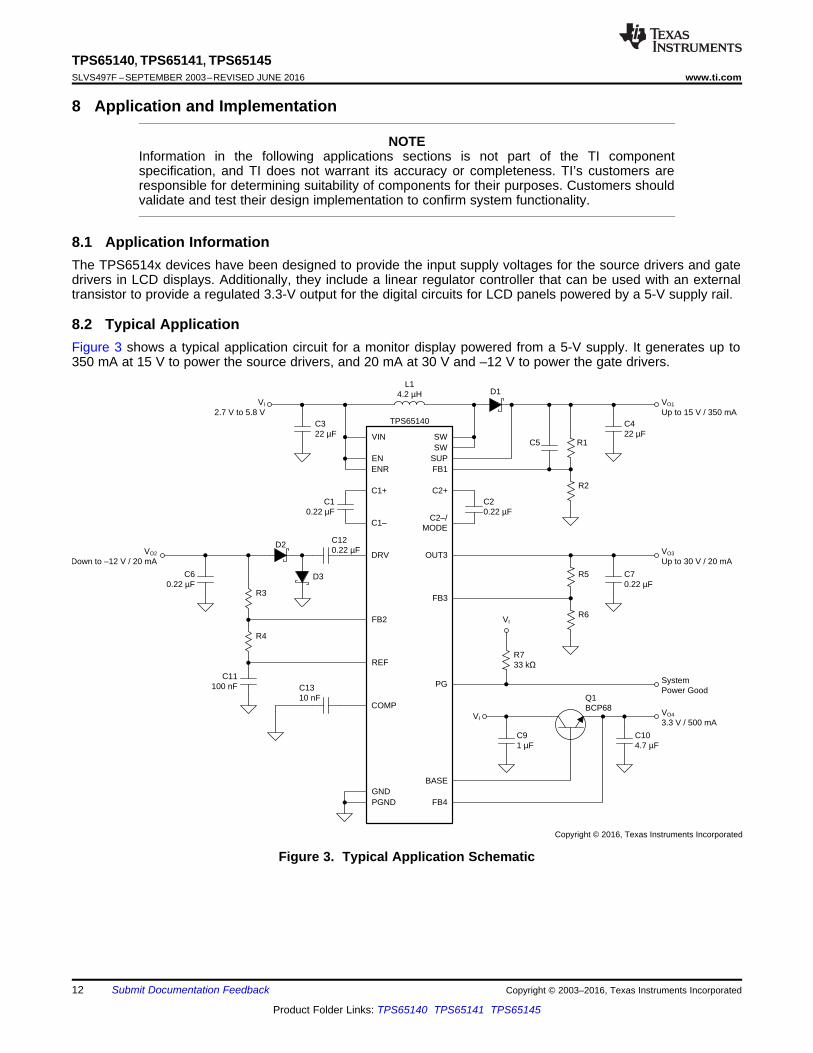
8.1 Application InformationThe TPS6514x devices have been designed to provide the input supply voltages for the source drivers and gatedrivers in LCD displays. Additionally, they include a linear regulator controller that can be used with an externaltransistor to provide a regulated 3.3-V output for the digital circuits for LCD panels powered by a 5-V supply rail.
8.2 Typical ApplicationFigure 3 shows a typical application circuit for a monitor display powered from a 5-V supply. It generates up to350 mA at 15 V to power the source drivers, and 20 mA at 30 V and –12 V to power the gate drivers.
Figure 3. Typical Application Schematic

LSWPeak L
I 304 mAI I 1.11 A 1.26 A
2 2
D= + = + =
( ) ( )IN SWL
S
V V D 3.3 V 0.5 V 0.73I 304 mA
f L 1.6 MHz 4.2 µH
- ´ - ´D = = =
´ ´
OUTL
I 300 mAI 1.11 A
1 D 1 0.73= = =
- -
OUT D IN
OUT D SW
V V V 10 V 0.8 V 3.3 VD 0.73
V V V 10 V 0.8 V 0.5 V
- + - += = =
- + - +
13
TPS65140, TPS65141, TPS65145www.ti.com SLVS497F –SEPTEMBER 2003–REVISED JUNE 2016
Product Folder Links: TPS65140 TPS65141 TPS65145
Submit Documentation FeedbackCopyright © 2003–2016, Texas Instruments Incorporated
Typical Application (continued)8.2.1 Design RequirementsTable 1 shows the design parameters for this example.
Table 1. Design RequirementsPARAMETER VALUE
VI Input supply voltage 2.7 V to 5.8 VVO1 Boost converter output voltage and current Up to 15 V at 350 mAVO3 Positive charge pump output voltage and current Up to 30 V at 20 mA
VO2 Negative charge pump output voltage and current Down to –12 V at 20mA
VO4 Linear regulator controller output voltage and current 3.3 V at 500 mA
8.2.2 Detailed Design Procedure
8.2.2.1 Boost Converter Design ProcedureThe first step in the design procedure is to calculate the maximum possible output current of the main boostconverter under certain input and output voltage conditions. The following is an example for a 3.3-V to 10-Vconversion:
VIN = 3.3 V, VOUT = 10 V, Switch voltage drop VSW = 0.5 V, Schottky diode forward voltage VD = 0.8 V1. Duty cycle:
(1)2. Average inductor current:
(2)3. Inductor peak-to-peak ripple current:
(3)4. Peak switch current:
(4)
The integrated switch, the inductor, and the external Schottky diode must be able to handle the peak switchcurrent. The calculated peak switch current must be equal to or lower than the minimum N-MOSFET switchcurrent limit as specified in Electrical Characteristics (1.6 A for the TPS65140 and TPS65141 and 0.96 A for theTPS65145). If the peak switch current is higher, then the converter cannot support the required load current. Thiscalculation must be done for the minimum input voltage where the peak switch current is highest. The calculationincludes conduction losses like switch rDS(on) (0.5 V) and diode forward drop voltage losses (0.8 V). Additionalswitching losses, inductor core and winding losses, and so forth, require a slightly higher peak switch current inthe actual application. The above calculation still allows for a good design and component selection.
8.2.2.1.1 Inductor Selection
Several inductors work with the TPS6514x. Especially with the external compensation, the performance can beadjusted to the specific application requirements. The main parameter for the inductor selection is the saturationcurrent of the inductor which must be higher than the peak switch current as calculated above with additionalmargin to cover for heavy load transients and extreme start-up conditions. Another method is to choose theinductor with a saturation current at least as high as the minimum switch current limit of 1.6 A for the TPS65140and TPS65141 and 0.96 A for the TPS65145. The different switch current limits allow selection of a physicallysmaller inductor when less output current is required. The second important parameter is the inductor DCresistance. Usually, the lower the DC resistance, the higher the efficiency. However, the inductor DC resistanceis not the only parameter determining the efficiency. Especially for a boost converter where the inductor is the

OUT POUT P
OUT S OUT D IN
I I L1V I ESR
C f V V V
æ ö´D = ´ - + ´ç ÷
+ -è ø
14
TPS65140, TPS65141, TPS65145SLVS497F –SEPTEMBER 2003–REVISED JUNE 2016 www.ti.com
Product Folder Links: TPS65140 TPS65141 TPS65145
Submit Documentation Feedback Copyright © 2003–2016, Texas Instruments Incorporated
energy storage element, the type and material of the inductor influences the efficiency as well. Especially at highswitching frequencies of 1.6 MHz, inductor core losses, proximity effects, and skin effects become moreimportant. Usually, an inductor with a larger form factor yields higher efficiency. The efficiency differencebetween different inductors can vary from 2% to 10%. For the TPS6514x, inductor values from 3.3 µH to 6.8 µHare a good choice but other values can be used as well. Possible inductors are shown in Table 2.
Table 2. Inductor SelectionDEVICE INDUCTOR VALUE COMPONENT SUPPLIER DIMENSIONS / mm ISAT/DCR
TPS65140
4.7 µH Coilcraft DO1813P-472HC 8.89 × 6.1 × 5 2.6 A, 54 mΩ4.2 µH Sumida CDRH5D28 4R2 5.7 × 5.7 × 3 2.2 A, 23 mΩ4.7 µH Sumida CDC5D23 4R7 6 × 6 × 2.5 1.6 A, 48 mΩ3.3 µH Wuerth Elektronik 744042003 4.8 × 4.8 × 2 1.8 A, 65 mΩ4.2 µH Sumida CDRH6D12 4R2 6.5 × 6.5 × 1.5 1.8 A, 60 mΩ3.3 µH Sumida CDRH6D12 3R3 6.5 × 6.5 × 1.5 1.9 A, 50 mΩ
TPS65145
3.3 µH Sumida CDPH4D19 3R3 5.1 × 5.1 × 2 1.5 A, 26 mΩ3.3 µH Coilcraft DO1606T-332 6.5 × 5.2 × 2 1.4 A, 120 mΩ3.3 µH Sumida CDRH2D18/HP 3R3 3.2 × 3.2 × 2 1.45 A, 69 mΩ4.7 µH Wuerth Elektronik 744010004 5.5 × 3.5 × 1 1 A, 260 mΩ3.3 µH Coilcraft LPO6610-332M 6.6 × 5.5 × 1 1.3 A, 160 mΩ
8.2.2.1.2 Output Capacitor Selection
For best output voltage filtering, TI recommends a low-ESR output capacitor. Ceramic capacitors have a lowESR value but depending on the application, tantalum capacitors can be used as well. A 22-µF ceramic outputcapacitor works for most of the applications. Higher capacitor values can be used to improve load transientregulation. See Table 2 for the selection of the output capacitor. The output voltage ripple can be calculated as:
where• IP = Peak switch current as calculated in the previous section with ISW(peak)
• L = Selected inductor value• IOUT = Normal load current• fS = Switching frequency• VD = Rectifier diode forward voltage (typical 0.3 V)• COUT = Selected output capacitor• ESR = Output capacitor ESR value (5)
8.2.2.1.3 Input Capacitor Selection
For good input voltage filtering, TI recommends low-ESR ceramic capacitors. A 22-µF ceramic input capacitor issufficient for most of applications. For better input voltage filtering, this value can be increased. See Table 3 andthe typical applications for input capacitor recommendations.
Table 3. Input and Output Capacitors SelectionCAPACITOR VOLTAGE RATING COMPONENT SUPPLIER COMMENTS
22 µF, 1210 16 V Taiyo Yuden EMK325BY226MM CO
22 µF, 1206 6.3 V Taiyo Yuden JMK316BJ226 CI
Z
1 1C8
2 f R1 2 50 kHz R1= =
´ p ´ ´ ´ p ´ ´
L14.7 µH
SWSW
TPS65140
D1
C422 µF
C56.8 pF
R1430 k
R256 k
FB1SUP
C2+
C2±/MODE
VO1
10 V / 150 mA
0.22 F
Copyright © 2016, Texas Instruments Incorporated
OUT
R1V 1.146 V 1
R2
æ ö= ´ +ç ÷
è ø
15
TPS65140, TPS65141, TPS65145www.ti.com SLVS497F –SEPTEMBER 2003–REVISED JUNE 2016
Product Folder Links: TPS65140 TPS65141 TPS65145
Submit Documentation FeedbackCopyright © 2003–2016, Texas Instruments Incorporated
8.2.2.1.4 Rectifier Diode Selection
To achieve high efficiency, a Schottky diode must be used. The voltage rating must be higher than the maximumoutput voltage of the converter. The average forward current must be equal to the average inductor current of theconverter. The main parameter influencing the efficiency of the converter is the forward voltage and the reverseleakage current of the diode; both must be as low as possible. Possible diodes are: On SemiconductorMBRM120L, Microsemi UPS120E, and Fairchild Semiconductor MBRS130L.
8.2.2.1.5 Converter Loop Design and Stability
The TPS6514x converter loop can be externally compensated and allows access to the internaltransconductance error amplifier output at the COMP pin. A small feedforward capacitor across the upperfeedback resistor divider speeds up the circuit as well. To test the converter stability and load transientperformance of the converter, a load step from 50 mA to 250 mA is applied, and the output voltage of theconverter is monitored. Applying load steps to the converter output is a good tool to judge the stability of such aboost converter.
8.2.2.1.6 Design Procedure Quick Steps1. Select the feedback resistor divider to set the output voltage.2. Select the feedforward capacitor to place a zero at 50 kHz.3. Select the compensation capacitor on pin COMP. The smaller the value, the higher the low frequency gain.4. Use a 50-kΩ potentiometer in series to CC and monitor VOUT during load transients. Fine tune the load
transient by adjusting the potentiometer. Select a resistor value that comes closest to the potentiometerresistor value. This must be done at the highest Vin and highest load current because stability is most criticalat these conditions.
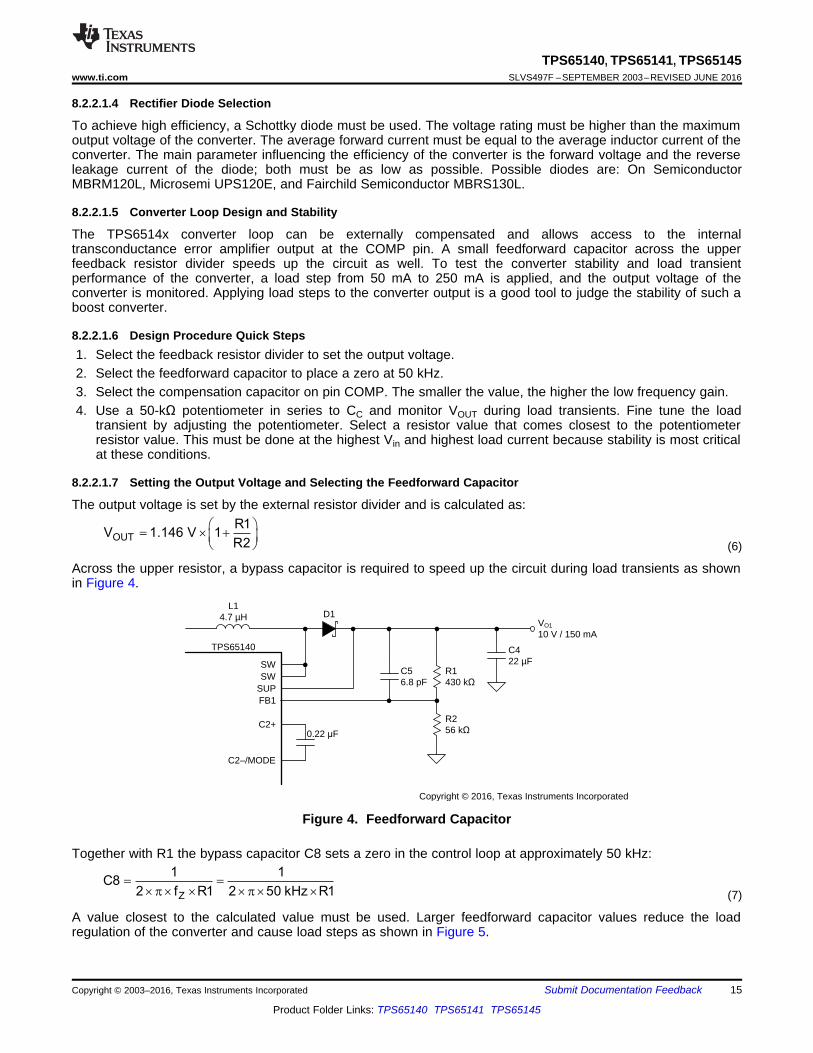
8.2.2.1.7 Setting the Output Voltage and Selecting the Feedforward Capacitor
The output voltage is set by the external resistor divider and is calculated as:
(6)
Across the upper resistor, a bypass capacitor is required to speed up the circuit during load transients as shownin Figure 4.
Figure 4. Feedforward Capacitor
Together with R1 the bypass capacitor C8 sets a zero in the control loop at approximately 50 kHz:
(7)
A value closest to the calculated value must be used. Larger feedforward capacitor values reduce the loadregulation of the converter and cause load steps as shown in Figure 5.

CC = 4.7 nFCC = 1 nF
Z
C C
1f
2 C R=
´ p ´ ´
COMP
CC
1 nFRC
15 k
Load Step
16
TPS65140, TPS65141, TPS65145SLVS497F –SEPTEMBER 2003–REVISED JUNE 2016 www.ti.com
Product Folder Links: TPS65140 TPS65141 TPS65145
Submit Documentation Feedback Copyright © 2003–2016, Texas Instruments Incorporated
Figure 5. Load Step Caused by a Too Large Feedforward Capacitor Value
8.2.2.1.8 Compensation
The regulator loop can be compensated by adjusting the external components connected to the COMP pin. TheCOMP pin is connected to the output of the internal transconductance error amplifier. A typical compensationscheme is shown in Figure 6.
Figure 6. Compensation Network
The compensation capacitor CC adjusts the low frequency gain, and the resistor value adjusts the high frequencygain. The following formula calculates at what frequency the resistor increases the high frequency gain.
(8)
Lower input voltages require a higher gain and a lower compensation capacitor value. A good start is CC = 1 nFfor a 3.3-V input and CC = 2.2 nF for a 5-V input. If the device operates over the entire input voltage range from2.7 V to 5.8 V, TI recommends a larger compensation capacitor up to 10 nF. Figure 7 shows the load transientwith a larger compensation capacitor, and Figure 8 shows a smaller compensation capacitor.
Figure 7. CC = 4.7 nF Figure 8. CC = 1 nF

R3 = R4 x = R4 x|VOUT| |VOUT|
VREF 1.213
V = -V xOUT REF = -1.213 V x
R R3 3
R R4 4
17
TPS65140, TPS65141, TPS65145www.ti.com SLVS497F –SEPTEMBER 2003–REVISED JUNE 2016
Product Folder Links: TPS65140 TPS65141 TPS65145
Submit Documentation FeedbackCopyright © 2003–2016, Texas Instruments Incorporated
Lastly, RC must be selected. A good practice is to use a 50-kΩ potentiometer and adjust the potentiometer forthe best load transient where no oscillations should occur. These tests have to be done at the highest VIN andhighest load current because the converter stability is most critical under these conditions. Figure 9, Figure 10,and Figure 11 show the fine tuning of the loop with RC.
Figure 9. Overcompensated (Damped Oscillation),RC is Too Large
Figure 10. Undercompensated (Loop is Too Slow),RC is Too Small
Figure 11. Optimum, RC is Ideal
8.2.2.1.9 Negative Charge Pump
The negative charge pump provides a regulated output voltage by inverting the main output voltage, VO1. Thenegative charge pump output voltage is set with external feedback resistors.
The maximum load current of the negative charge pump depends on the voltage drop across the externalSchottky diodes, the internal ON-resistance of the charge pump MOSFETS Q8 and Q9, and the impedance ofthe flying capacitor, C12. When the voltage drop across these components is larger than the voltage differencefrom VO1 to VO2, the charge pump is in drop out, providing the maximum possible output current. Therefore, thehigher the voltage difference between VO1 and VO2, the higher the possible load current. See Figure 21 for thepossible output current versus boost converter voltage VO1 and the calculations below.
VOUTmin = –(VO1 – 2 VF – IO (2 × rDS(on)Q8 + 2 × rDS(on)Q9 + Xcfly)) (9)
Setting the output voltage:
(10)
(11)

OUT OUT
FB
V VR5 R6 1 R6 1
V 1.214
æ ö æ ö= ´ - = ´ -ç ÷ ç ÷
è øè ø
OUT
R5V 1.214 1
R6
æ ö= ´ +ç ÷
è ø
18
TPS65140, TPS65141, TPS65145SLVS497F –SEPTEMBER 2003–REVISED JUNE 2016 www.ti.com
Product Folder Links: TPS65140 TPS65141 TPS65145
Submit Documentation Feedback Copyright © 2003–2016, Texas Instruments Incorporated
The lower feedback resistor value, R4, must be in a range from 40 kΩ to 120 kΩ or the overall feedbackresistance must be within 500 kΩ to 1 MΩ. Smaller values load the reference too heavy and larger values maycause stability problems. The negative charge pump requires two external Schottky diodes. The peak currentrating of the Schottky diode must be twice the load current of the output. For a 20-mA output current, the dualSchottky diode BAT54 or similar is a good choice.
8.2.2.1.10 Positive Charge Pump
The positive charge pump can be operated in a voltage doubler mode or a voltage tripler mode depending on theconfiguration of the C2+ and C2–/MODE pins. Leaving the C2+ pin open and connecting C2-/MODE to GNDforces the positive charge pump to operate in a voltage doubler mode. If higher output voltages are required thepositive charge pump can be operated as a voltage tripler. To operate the charge pump in the voltage triplermode, a flying capacitor must be connected to C2+ and C2–/MODE.
The maximum load current of the positive charge pump depends on the voltage drop across the internal Schottkydiodes, the internal ON-resistance of the charge pump MOSFETS, and the impedance of the flying capacitor.When the voltage drop across these components is larger than the voltage difference VO1 × 2 to VO3 (doublermode) or VO1 × 3 to VO3 (tripler mode), then the charge pump is in dropout, providing the maximum possibleoutput current. Therefore, the higher the voltage difference between VO1 x 2 (doubler) or VO1 × 3 (tripler) to VO3,the higher the possible load current. See Figure 22 and Figure 23 for output current versus boost convertervoltage, VO1, and the following calculations.
Voltage doubler:VO3max = 2 × VO1 – (2 VF + 2 × IO × (2 × rDS(on)Q5 + rDS(on)Q3 + rDS(on)Q4 + XC1)) (12)
Voltage tripler:VO3max = 3 × VO – (4 × VF + 2 × IO × (3 × rDS(on)Q5 + rDS(on)Q3 + rDS(on)Q4 + XC1 + XC2)) (13)
The output voltage is set by the external resistor divider and is calculated as:
(14)
(15)
8.2.2.1.11 Linear Regulator Controller
The TPS6514x includes a linear regulator controller to generate a 3.3-V rail when the system is powered from a5-V supply. Because an external NPN transistor is required, the input voltage of the TPS6514x applied to VINmust be higher than the output voltage of the regulator. To provide a minimum base drive current of 13.5 mA, aminimum internal voltage drop of 500 mV from VI to VBASE is required. This can be translated into a minimuminput voltage on VIN for a certain output voltage as the following calculation shows:
VI(min) = VO4 + VBE + 0.5 V (16)
The base drive current together with the hFE of the external transistor determines the possible output current.Using a standard NPN transistor like the BCP68 allows an output current of 1 A and using the BCP54 allows aload current of 337 mA for an input voltage of 5 V. Other transistors can be used as well, depending on therequired output current, power dissipation, and PCB space. The device is stable with a 4.7-µF ceramic outputcapacitor. Larger output capacitor values can be used to improve the load transient response when higher loadcurrents are required.

VSW
10 V/div
VO
50 mV/div
VI = 3.3 V
VO = 10 V/10 mA
IL
500 mA/div
250 ns/div
Vo1
200 mV/div
VI = 3.3 V
Vo1 = 10 V, CO= 22 mF
IO
50 mA to 250 mA
100 s/divm
VSW
10 V/div
VO
50 mV/div
VI = 3.3 V
VO = 10 V/300 mA
IL
1 A/div
250 ns/div
70
75
80
85
90
95
100
2.5 3 3.5 4 4.5 5 5.5 6
Vo1 = 6 V
Vo1 = 15 V
Vo1 = 10 V
ILoad at Vo1 = 100 mA
Vo2, Vo3 = No Load, Switching
VI - Input Voltage - V
Eff
icie
ncy -
%
10
20
30
40
50
60
70
80
90
100
1 10 100 1 k
Vo1 = 6 V
IL − Load Current − mA
Eff
icie
ncy
−%
Vo1 = 15 V
Vo1 = 10 V
VI = 3.3 V
Vo2, Vo3 = No Load, Switching10
20
30
40
50
60
70
80
90
100
1 10 100 1 k
IL − Load Current − mA
Eff
icie
ncy
−%
Vo1 = 15 V
Vo1 = 10 V
VI = 5 V
Vo2, Vo3 = No Load, Switching
19
TPS65140, TPS65141, TPS65145www.ti.com SLVS497F –SEPTEMBER 2003–REVISED JUNE 2016
Product Folder Links: TPS65140 TPS65141 TPS65145
Submit Documentation FeedbackCopyright © 2003–2016, Texas Instruments Incorporated
8.2.3 Application Curves
Figure 12. Efficiency vs Load Current Figure 13. Efficiency vs Load Current
Figure 14. Efficiency vs Input Voltage Figure 15. PWM Operation Continuous Mode
Figure 16. PWM Operation at Light Load Figure 17. Load Transient Response

0
0.02
0.04
0.06
0.08
0.10
0.12
0.14
9 10 11 12 13 14 15
Vo1 − Output Voltage − V
−O
utp
ut
Cu
rren
t−
AI O
Vo3 = 18 V (Doubler Mode)
TA = 25°C
TA = 85°CTA = −40°C
0
0.02
0.04
0.06
0.08
0.10
0.12
9 10 11 12 13 14 15
Vo1 − Output Voltage − V
−O
utp
ut
Cu
rren
t−
AI O
Vo3 = 28 V (Tripler Mode)
TA = 25°C
TA = 85°C
TA = −40°C
Vo1
5 V/div
VI = 3.3 V
VO = 10 V,
IO = 300 mA
500 s/divm
I
I
500
mA/div0
0.02
0.04
0.06
0.08
0.10
0.12
0.14
0.16
0.18
0.20
8.8 9.8 10.8 11.8 12.8 13.8 14.8
Vo1 − Output Voltage − V
−O
utp
ut
Cu
rren
t−
AI O
Vo2 = −8 V
TA = −40°C
TA = 25°C
TA = 85°C
Vo1
5 V/div
VI = 3.3 V
VO = 10 V,
500 s/divm
Vo2
5 V/div
Vo3
10 V/div
Vo1
100 mV/div
VI = 3.3 V
Vo1 = 10 V, CO= 2*22 mF
IO
50 mA to 250 mA
100 s/divm
20
TPS65140, TPS65141, TPS65145SLVS497F –SEPTEMBER 2003–REVISED JUNE 2016 www.ti.com
Product Folder Links: TPS65140 TPS65141 TPS65145
Submit Documentation Feedback Copyright © 2003–2016, Texas Instruments Incorporated
Figure 18. Load Transient Response Figure 19. Power-Up Sequencing
Figure 20. Soft Start VO1 Figure 21. VO2 Maximum Load Current
Figure 22. VO3 Maximum Load Current Figure 23. VO3 Maximum Load Current

VINENENR
L13.3 µH
SWSW
TPS65140C322 µF
VI
3.3 V
D1
C422 µF
C56.8 pF
R1430 N
R256 k
FB1
VO1
10 V / 150 mA
SUP
C20.22 µF
C2+
C2±/MODE
C70.22 µF
VO3
23 V / 20 mAR51 M
R656 k
OUT3
FB3
R733 k
VI
PGSystemPower Good
GNDPGND
C1+C1
0.22 µFC1±
DRV
C60.22 µF
R3620 k
R4150 k
FB2
REF
C110.22 µF
D2
D3
C120.22 µF
BASE
FB4
COMP
C131 nF
VO2
±5 V / 20 mA
R715 k
Copyright © 2016, Texas Instruments Incorporated
21
TPS65140, TPS65141, TPS65145www.ti.com SLVS497F –SEPTEMBER 2003–REVISED JUNE 2016
Product Folder Links: TPS65140 TPS65141 TPS65145
Submit Documentation FeedbackCopyright © 2003–2016, Texas Instruments Incorporated
8.3 System Examples
Figure 24. Typical Application, Notebook Supply

VIN
ENENR
L14.7 µH
SWSW
TPS65140C322 µF
VI
5 V
D1
C422 µF
C53.3 pF
R1820 N
R275 N
FB1
VO1
13.5 V / 400 mA
SUP
C2+
C2±/MODE
C70.22 µF
VO3
23 V / 20 mA
R51 0
R656 N
OUT3
FB3
R733 k
VI
PG SystemPower Good
GNDPGND
C1+C1
0.22 µFC1±
DRV
C60.22 µF
R3750 N
R4130 N
FB2
REF
C110.22 µF
D2
D3
C120.22 µF
C104.7 µF
C91 µF
VIVO4
3.3 V / 500 mA
BASE
FB4
Q1BCP68COMP
C132.2 nF
VO2
±7 V / 20 mA
R74.3 k
Copyright © 2016, Texas Instruments Incorporated
22
TPS65140, TPS65141, TPS65145SLVS497F –SEPTEMBER 2003–REVISED JUNE 2016 www.ti.com
Product Folder Links: TPS65140 TPS65141 TPS65145
Submit Documentation Feedback Copyright © 2003–2016, Texas Instruments Incorporated
System Examples (continued)
Figure 25. Typical Application, Monitor Supply
9 Power Supply RecommendationsThe TPS6514x devices are designed to operate from an input voltage supply range from 2.7 V to 5.8 V. Thisinput supply must be well regulated. The input capacitance shown in the application schematics in this data sheetis sufficient for typical applications.

23
TPS65140, TPS65141, TPS65145www.ti.com SLVS497F –SEPTEMBER 2003–REVISED JUNE 2016
Product Folder Links: TPS65140 TPS65141 TPS65145
Submit Documentation FeedbackCopyright © 2003–2016, Texas Instruments Incorporated
10 Layout
10.1 Layout GuidelinesFor all switching power supplies, the layout is an important step in the design, especially at high-peak currentsand switching frequencies. If the layout is not carefully designed, the regulator might show stability and EMIproblems. TI recommends the following PCB layout guidelines for the TPS6514x devices:• Connect PGND and AGND together on the same ground plane.• Connect all capacitor grounds and PGND together on a common ground plane.• Place the input filter capacitor as close as possible to the input pin of the IC.• Route first the traces carrying high-switching currents with wide and short traces.• Isolate analog signal paths from power paths.• If vias are necessary, try to use more than one in parallel to decrease parasitics, especially for power traces.• Solder the thermal pad to the PCB for good thermal performance
10.2 Layout Example
Figure 26. PCB Layout Example
10.3 Thermal ConsiderationsAn influential component of the thermal performance of a package is board design. To take full advantage of theheat dissipation abilities of the PowerPAD or VQFN package with exposed thermal die, a board that acts similarto a heatsink and allows for the use of an exposed (and solderable) deep downset pad must be used. For furtherinformation, see Texas Instruments application notes PowerPAD Thermally Enhanced Package and Power PadMade Easy. For the VQFN package, see the application report QFN/SON PCB Attachement. Especially for theVQFN package, it is required to solder down the thermal pad to achieve the required thermal resistance.

24
TPS65140, TPS65141, TPS65145SLVS497F –SEPTEMBER 2003–REVISED JUNE 2016 www.ti.com
Product Folder Links: TPS65140 TPS65141 TPS65145
Submit Documentation Feedback Copyright © 2003–2016, Texas Instruments Incorporated
11 Device and Documentation Support
11.1 Device Support
11.1.1 Third-Party Products DisclaimerTI'S PUBLICATION OF INFORMATION REGARDING THIRD-PARTY PRODUCTS OR SERVICES DOES NOTCONSTITUTE AN ENDORSEMENT REGARDING THE SUITABILITY OF SUCH PRODUCTS OR SERVICESOR A WARRANTY, REPRESENTATION OR ENDORSEMENT OF SUCH PRODUCTS OR SERVICES, EITHERALONE OR IN COMBINATION WITH ANY TI PRODUCT OR SERVICE.
11.2 Documentation Support
11.2.1 Related DocumentationFor related documentation see the following:• PowerPAD Thermally Enhanced Package (SLMA002)• Power Pad Made Easy (SLMA004)• QFN/SON PCB Attachement (SLUA271)
11.3 Related LinksThe table below lists quick access links. Categories include technical documents, support and communityresources, tools and software, and quick access to sample or buy.
Table 4. Related Links
PARTS PRODUCT FOLDER SAMPLE & BUY TECHNICALDOCUMENTS
TOOLS &SOFTWARE
SUPPORT &COMMUNITY
TPS65140 Click here Click here Click here Click here Click hereTPS65141 Click here Click here Click here Click here Click hereTPS65145 Click here Click here Click here Click here Click here
11.4 Receiving Notification of Documentation UpdatesTo receive notification of documentation updates, navigate to the device product folder on ti.com. In the upperright corner, click on Alert me to register and receive a weekly digest of any product information that haschanged. For change details, review the revision history included in any revised document.
11.5 Community ResourcesThe following links connect to TI community resources. Linked contents are provided "AS IS" by the respectivecontributors. They do not constitute TI specifications and do not necessarily reflect TI's views; see TI's Terms ofUse.
TI E2E™ Online Community TI's Engineer-to-Engineer (E2E) Community. Created to foster collaborationamong engineers. At e2e.ti.com, you can ask questions, share knowledge, explore ideas and helpsolve problems with fellow engineers.
Design Support TI's Design Support Quickly find helpful E2E forums along with design support tools andcontact information for technical support.
11.6 TrademarksPowerPAD, E2E are trademarks of Texas Instruments.All other trademarks are the property of their respective owners.
11.7 Electrostatic Discharge CautionThese devices have limited built-in ESD protection. The leads should be shorted together or the device placed in conductive foamduring storage or handling to prevent electrostatic damage to the MOS gates.

25
TPS65140, TPS65141, TPS65145www.ti.com SLVS497F –SEPTEMBER 2003–REVISED JUNE 2016
Product Folder Links: TPS65140 TPS65141 TPS65145
Submit Documentation FeedbackCopyright © 2003–2016, Texas Instruments Incorporated
11.8 GlossarySLYZ022 — TI Glossary.
This glossary lists and explains terms, acronyms, and definitions.
12 Mechanical, Packaging, and Orderable InformationThe following pages include mechanical, packaging, and orderable information. This information is the mostcurrent data available for the designated devices. This data is subject to change without notice and revision ofthis document. For browser-based versions of this data sheet, refer to the left-hand navigation.

PACKAGE OPTION ADDENDUM
www.ti.com 10-Dec-2020
Addendum-Page 1
PACKAGING INFORMATION
Orderable Device Status(1)
Package Type PackageDrawing
Pins PackageQty
Eco Plan(2)
Lead finish/Ball material
(6)
MSL Peak Temp(3)
Op Temp (°C) Device Marking(4/5)
Samples
TPS65140PWP ACTIVE HTSSOP PWP 24 60 RoHS & Green NIPDAU Level-2-260C-1 YEAR -40 to 85 TPS65140
TPS65140PWPR ACTIVE HTSSOP PWP 24 2000 RoHS & Green NIPDAU Level-2-260C-1 YEAR -40 to 85 TPS65140
TPS65140RGER ACTIVE VQFN RGE 24 3000 RoHS & Green NIPDAU Level-2-260C-1 YEAR -40 to 85 TPS65140
TPS65141PWP ACTIVE HTSSOP PWP 24 60 RoHS & Green NIPDAU Level-2-260C-1 YEAR -40 to 85 TPS65141
TPS65141PWPR ACTIVE HTSSOP PWP 24 2000 RoHS & Green NIPDAU Level-2-260C-1 YEAR -40 to 85 TPS65141
TPS65141RGER ACTIVE VQFN RGE 24 3000 RoHS & Green NIPDAU Level-2-260C-1 YEAR -40 to 85 TPS65141
TPS65145PWP ACTIVE HTSSOP PWP 24 60 RoHS & Green NIPDAU Level-2-260C-1 YEAR -40 to 85 TPS65145
TPS65145PWPR ACTIVE HTSSOP PWP 24 2000 RoHS & Green NIPDAU Level-2-260C-1 YEAR -40 to 85 TPS65145
TPS65145RGER ACTIVE VQFN RGE 24 3000 RoHS & Green NIPDAU Level-2-260C-1 YEAR -40 to 85 TPS65145
(1) The marketing status values are defined as follows:ACTIVE: Product device recommended for new designs.LIFEBUY: TI has announced that the device will be discontinued, and a lifetime-buy period is in effect.NRND: Not recommended for new designs. Device is in production to support existing customers, but TI does not recommend using this part in a new design.PREVIEW: Device has been announced but is not in production. Samples may or may not be available.OBSOLETE: TI has discontinued the production of the device.
(2) RoHS: TI defines "RoHS" to mean semiconductor products that are compliant with the current EU RoHS requirements for all 10 RoHS substances, including the requirement that RoHS substancedo not exceed 0.1% by weight in homogeneous materials. Where designed to be soldered at high temperatures, "RoHS" products are suitable for use in specified lead-free processes. TI mayreference these types of products as "Pb-Free".RoHS Exempt: TI defines "RoHS Exempt" to mean products that contain lead but are compliant with EU RoHS pursuant to a specific EU RoHS exemption.Green: TI defines "Green" to mean the content of Chlorine (Cl) and Bromine (Br) based flame retardants meet JS709B low halogen requirements of <=1000ppm threshold. Antimony trioxide basedflame retardants must also meet the <=1000ppm threshold requirement.
(3) MSL, Peak Temp. - The Moisture Sensitivity Level rating according to the JEDEC industry standard classifications, and peak solder temperature.
(4) There may be additional marking, which relates to the logo, the lot trace code information, or the environmental category on the device.

PACKAGE OPTION ADDENDUM
www.ti.com 10-Dec-2020
Addendum-Page 2
(5) Multiple Device Markings will be inside parentheses. Only one Device Marking contained in parentheses and separated by a "~" will appear on a device. If a line is indented then it is a continuationof the previous line and the two combined represent the entire Device Marking for that device.
(6) Lead finish/Ball material - Orderable Devices may have multiple material finish options. Finish options are separated by a vertical ruled line. Lead finish/Ball material values may wrap to twolines if the finish value exceeds the maximum column width.
Important Information and Disclaimer:The information provided on this page represents TI's knowledge and belief as of the date that it is provided. TI bases its knowledge and belief on informationprovided by third parties, and makes no representation or warranty as to the accuracy of such information. Efforts are underway to better integrate information from third parties. TI has taken andcontinues to take reasonable steps to provide representative and accurate information but may not have conducted destructive testing or chemical analysis on incoming materials and chemicals.TI and TI suppliers consider certain information to be proprietary, and thus CAS numbers and other limited information may not be available for release.
In no event shall TI's liability arising out of such information exceed the total purchase price of the TI part(s) at issue in this document sold by TI to Customer on an annual basis.
OTHER QUALIFIED VERSIONS OF TPS65140, TPS65145 :
• Automotive: TPS65140-Q1, TPS65145-Q1
NOTE: Qualified Version Definitions:
• Automotive - Q100 devices qualified for high-reliability automotive applications targeting zero defects

TAPE AND REEL INFORMATION
*All dimensions are nominal
Device PackageType
PackageDrawing
Pins SPQ ReelDiameter
(mm)
ReelWidth
W1 (mm)
A0(mm)
B0(mm)
K0(mm)
P1(mm)
W(mm)
Pin1Quadrant
TPS65140PWPR HTSSOP PWP 24 2000 330.0 16.4 6.95 8.3 1.6 8.0 16.0 Q1
TPS65140RGER VQFN RGE 24 3000 330.0 12.4 4.25 4.25 1.15 8.0 12.0 Q2
TPS65141PWPR HTSSOP PWP 24 2000 330.0 16.4 6.95 8.3 1.6 8.0 16.0 Q1
TPS65141RGER VQFN RGE 24 3000 330.0 12.4 4.25 4.25 1.15 8.0 12.0 Q2
TPS65145PWPR HTSSOP PWP 24 2000 330.0 16.4 6.95 8.3 1.6 8.0 16.0 Q1
TPS65145RGER VQFN RGE 24 3000 330.0 12.4 4.25 4.25 1.15 8.0 12.0 Q2
PACKAGE MATERIALS INFORMATION
www.ti.com 5-Jan-2022
Pack Materials-Page 1

*All dimensions are nominal
Device Package Type Package Drawing Pins SPQ Length (mm) Width (mm) Height (mm)
TPS65140PWPR HTSSOP PWP 24 2000 350.0 350.0 43.0
TPS65140RGER VQFN RGE 24 3000 853.0 449.0 35.0
TPS65141PWPR HTSSOP PWP 24 2000 350.0 350.0 43.0
TPS65141RGER VQFN RGE 24 3000 853.0 449.0 35.0
TPS65145PWPR HTSSOP PWP 24 2000 350.0 350.0 43.0
TPS65145RGER VQFN RGE 24 3000 853.0 449.0 35.0
PACKAGE MATERIALS INFORMATION
www.ti.com 5-Jan-2022
Pack Materials-Page 2

TUBE
*All dimensions are nominal
Device Package Name Package Type Pins SPQ L (mm) W (mm) T (µm) B (mm)
TPS65140PWP PWP HTSSOP 24 60 530 10.2 3600 3.5
TPS65141PWP PWP HTSSOP 24 60 530 10.2 3600 3.5
TPS65145PWP PWP HTSSOP 24 60 530 10.2 3600 3.5
PACKAGE MATERIALS INFORMATION
www.ti.com 5-Jan-2022
Pack Materials-Page 3

www.ti.com
GENERIC PACKAGE VIEW
This image is a representation of the package family, actual package may vary.Refer to the product data sheet for package details.
TSSOP - 1.2 mm max heightTMPowerPADPWP 24PLASTIC SMALL OUTLINE4.4 x 7.6, 0.65 mm pitch
4224742/B

www.ti.com
PACKAGE OUTLINE
C TYP6.66.2
22X 0.65
24X 0.300.19
2X7.15
(0.15) TYP
0 - 80.150.05
2.401.65
5.164.12
2X (0.95) MAXNOTE 5
1.2 MAX
(1)
0.25GAGE PLANE
0.750.50
A
NOTE 3
7.97.7
B 4.54.3
4X (0.2) MAXNOTE 5
4222709/A 02/2016
PowerPAD TSSOP - 1.2 mm max heightPWP0024BPLASTIC SMALL OUTLINE
NOTES: 1. All linear dimensions are in millimeters. Any dimensions in parenthesis are for reference only. Dimensioning and tolerancing per ASME Y14.5M. 2. This drawing is subject to change without notice. 3. This dimension does not include mold flash, protrusions, or gate burrs. Mold flash, protrusions, or gate burrs shall not exceed 0.15 mm per side.4. Reference JEDEC registration MO-153.5. Features may not be present and may vary.
PowerPAD is a trademark of Texas Instruments.
TM
124
0.1 C A B
1312
PIN 1 IDAREA
SEATING PLANE
0.1 C
SEE DETAIL A
DETAIL ATYPICAL
SCALE 2.200
EXPOSEDTHERMAL PAD

www.ti.com
EXAMPLE BOARD LAYOUT
(5.8)
0.05 MAXALL AROUND
0.05 MINALL AROUND
24X (1.5)
24X (0.45)
22X (0.65)
(3.4)NOTE 9
(7.8)NOTE 9
(2.4)
(5.16)
( ) TYPVIA
0.2
(1) TYP
(1.1)TYP
(R )TYP
0.05
4222709/A 02/2016
PowerPAD TSSOP - 1.2 mm max heightPWP0024BPLASTIC SMALL OUTLINE
SYMM
SYMM
SEE DETAILS
LAND PATTERN EXAMPLESCALE:10X
1
12 13
24
METAL COVEREDBY SOLDER MASK
SOLDER MASKDEFINED PAD
TM
NOTES: (continued) 6. Publication IPC-7351 may have alternate designs. 7. Solder mask tolerances between and around signal pads can vary based on board fabrication site. 8. This package is designed to be soldered to a thermal pad on the board. For more information, see Texas Instruments literature numbers SLMA002 (www.ti.com/lit/slma002) and SLMA004 (www.ti.com/lit/slma004).9. Size of metal pad may vary due to creepage requirement.
METALSOLDER MASKOPENING
NON SOLDER MASKDEFINED
SOLDER MASK DETAILSPADS 1-24
SOLDER MASKDEFINED
SOLDER MASKMETAL UNDER SOLDER MASK
OPENING

www.ti.com
EXAMPLE STENCIL DESIGN
24X (1.5)
24X (0.45)
(2.4)
(5.16)BASED ON
0.125 THICKSTENCIL
22X (0.65)
(R ) TYP0.05
(5.8)
4222709/A 02/2016
PowerPAD TSSOP - 1.2 mm max heightPWP0024BPLASTIC SMALL OUTLINE
2.03 X 4.360.1752.19 X 4.710.15
2.4 X 5.16 (SHOWN)0.1252.68 X 5.770.1
SOLDER STENCILOPENING
STENCILTHICKNESS
NOTES: (continued) 10. Laser cutting apertures with trapezoidal walls and rounded corners may offer better paste release. IPC-7525 may have alternate design recommendations. 11. Board assembly site may have different recommendations for stencil design.
TM
SYMM
SYMM
1
12 13
24
BASED ON0.125 THICK
STENCIL
BY SOLDER MASKMETAL COVERED
SEE TABLE FORDIFFERENT OPENINGSFOR OTHER STENCILTHICKNESSES
SOLDER PASTE EXAMPLEEXPOSED PAD
100% PRINTED SOLDER COVERAGE BY AREASCALE:10X

GENERIC PACKAGE VIEW
Images above are just a representation of the package family, actual package may vary.Refer to the product data sheet for package details.
RGE 24 VQFN - 1 mm max heightPLASTIC QUAD FLATPACK - NO LEAD
4204104/H

www.ti.com
PACKAGE OUTLINE
C
SEE TERMINALDETAIL
24X 0.30.2
2.45 0.1
24X 0.50.3
1 MAX
(0.2) TYP
0.050.00
20X 0.5
2X2.5
2X 2.5
A 4.13.9
B
4.13.9
0.30.2
0.50.3
VQFN - 1 mm max heightRGE0024BPLASTIC QUAD FLATPACK - NO LEAD
4219013/A 05/2017
PIN 1 INDEX AREA
0.08 C
SEATING PLANE
1
6 13
18
7 12
24 19
(OPTIONAL)PIN 1 ID
0.1 C A B0.05
EXPOSEDTHERMAL PAD
25 SYMM
SYMM
NOTES: 1. All linear dimensions are in millimeters. Any dimensions in parenthesis are for reference only. Dimensioning and tolerancing per ASME Y14.5M. 2. This drawing is subject to change without notice. 3. The package thermal pad must be soldered to the printed circuit board for thermal and mechanical performance.
SCALE 3.000
DETAILOPTIONAL TERMINAL
TYPICAL

www.ti.com
EXAMPLE BOARD LAYOUT
0.07 MINALL AROUND
0.07 MAXALL AROUND
24X (0.25)
24X (0.6)
( 0.2) TYPVIA
20X (0.5)
(3.8)
(3.8)
( 2.45)
(R0.05)TYP
(0.975) TYP
VQFN - 1 mm max heightRGE0024BPLASTIC QUAD FLATPACK - NO LEAD
4219013/A 05/2017
SYMM
1
6
7 12
13
18
1924
SYMM
LAND PATTERN EXAMPLEEXPOSED METAL SHOWN
SCALE:15X
NOTES: (continued) 4. This package is designed to be soldered to a thermal pad on the board. For more information, see Texas Instruments literature number SLUA271 (www.ti.com/lit/slua271).5. Vias are optional depending on application, refer to device data sheet. If any vias are implemented, refer to their locations shown on this view. It is recommended that vias under paste be filled, plugged or tented.
25
SOLDER MASKOPENING
METAL UNDERSOLDER MASK
SOLDER MASKDEFINED
EXPOSEDMETAL
METAL
SOLDER MASKOPENING
SOLDER MASK DETAILS
NON SOLDER MASKDEFINED
(PREFERRED)
EXPOSEDMETAL
www.ti.com
EXAMPLE STENCIL DESIGN
24X (0.6)
24X (0.25)
20X (0.5)
(3.8)
(3.8)
4X ( 1.08)
(0.64)TYP
(0.64) TYP
(R0.05) TYP
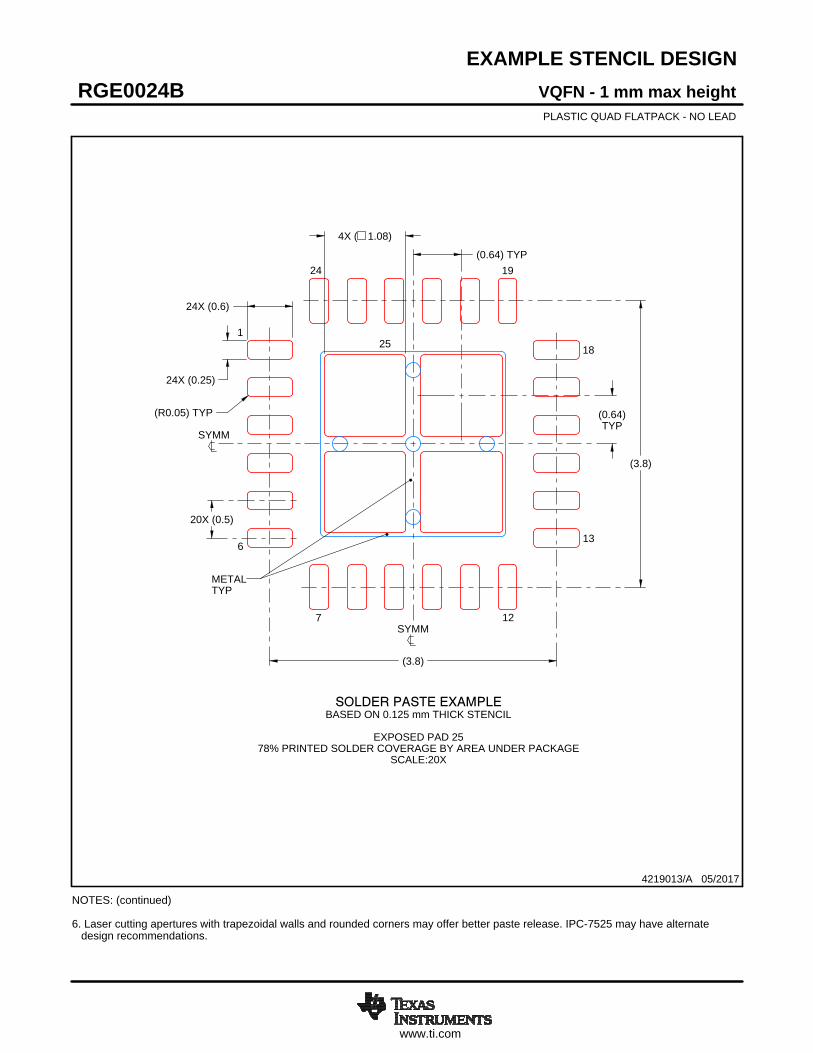
VQFN - 1 mm max heightRGE0024BPLASTIC QUAD FLATPACK - NO LEAD
4219013/A 05/2017
NOTES: (continued) 6. Laser cutting apertures with trapezoidal walls and rounded corners may offer better paste release. IPC-7525 may have alternate design recommendations.
25
SYMM
METALTYP
SOLDER PASTE EXAMPLEBASED ON 0.125 mm THICK STENCIL
EXPOSED PAD 25
78% PRINTED SOLDER COVERAGE BY AREA UNDER PACKAGESCALE:20X
SYMM
1
6
7 12
13
18
1924

IMPORTANT NOTICE AND DISCLAIMERTI PROVIDES TECHNICAL AND RELIABILITY DATA (INCLUDING DATA SHEETS), DESIGN RESOURCES (INCLUDING REFERENCE DESIGNS), APPLICATION OR OTHER DESIGN ADVICE, WEB TOOLS, SAFETY INFORMATION, AND OTHER RESOURCES “AS IS” AND WITH ALL FAULTS, AND DISCLAIMS ALL WARRANTIES, EXPRESS AND IMPLIED, INCLUDING WITHOUT LIMITATION ANY IMPLIED WARRANTIES OF MERCHANTABILITY, FITNESS FOR A PARTICULAR PURPOSE OR NON-INFRINGEMENT OF THIRD PARTY INTELLECTUAL PROPERTY RIGHTS.These resources are intended for skilled developers designing with TI products. You are solely responsible for (1) selecting the appropriate TI products for your application, (2) designing, validating and testing your application, and (3) ensuring your application meets applicable standards, and any other safety, security, regulatory or other requirements.These resources are subject to change without notice. TI grants you permission to use these resources only for development of an application that uses the TI products described in the resource. Other reproduction and display of these resources is prohibited. No license is granted to any other TI intellectual property right or to any third party intellectual property right. TI disclaims responsibility for, and you will fully indemnify TI and its representatives against, any claims, damages, costs, losses, and liabilities arising out of your use of these resources.TI’s products are provided subject to TI’s Terms of Sale or other applicable terms available either on ti.com or provided in conjunction with such TI products. TI’s provision of these resources does not expand or otherwise alter TI’s applicable warranties or warranty disclaimers for TI products.TI objects to and rejects any additional or different terms you may have proposed. IMPORTANT NOTICE
Mailing Address: Texas Instruments, Post Office Box 655303, Dallas, Texas 75265Copyright © 2022, Texas Instruments Incorporated