tps65000-q1 2.25-mhz step-down converter with dual …
TRANSCRIPT

VLDO1
SW
TPS65000-Q1
VINDCDCVIN
VIN
VINLDO2
EN_LDO2
VDCDC
10mF
2.2 Hm
10 Fm
470kW
EN_DCDC
EN_LDO1
VINLDO1
PGNDP
P
FB_DCDC
P
PG
MODE
470kW
180kW
FB_LDO1
AGNDA
A
A
10 Fm
P
VLDO2
820kW
180kW
FB_LDO2 10 Fm
P
680W
150kW
A
3.3V
VLDO1
1.8V
VLDO2
2.8V
22pF
Oscillator
SSCG
Bandgap Reference
TPS65000-Q1 Function/Pin
LDO1
300mA
LDO2300mA
A
Step-Down
600mA
VDCDC
PG
Product
Folder
Order
Now
Technical
Documents
Tools &
Software
Support &Community
An IMPORTANT NOTICE at the end of this data sheet addresses availability, warranty, changes, use in safety-critical applications,intellectual property matters and other important disclaimers. PRODUCTION DATA.
TPS65000-Q1SLVSC45C –AUGUST 2013–REVISED JUNE 2017
TPS65000-Q1 2.25-MHz Step-Down Converter With Dual LDOs
1
1 Features1• Qualified for Automotive Applications• AEC-Q100 Qualified With the Following Results:
– Device Temperature Grade 2:–40°C to +105°C Ambient OperatingTemperature Range
– Device HBM ESD Classification Level H2– Device CDM ESD Classification Level C4B
• Step-Down Converters:– VIN Range From 2.3 V to 6 V– Spread-Spectrum Clock (SSC) Generation for
Reduced EMI– 2.25-MHz Fixed-Frequency Operation– 600-mA Output Current
• LDOs:– VIN Range From 1.6 V to 6 V– Adjustable Output Voltage– Up to 300-mA Output Current– Separate Power Inputs and Enables
• 3-mm × 3-mm 16-Pin WQFN
2 Applications• Automotive Camera Module• Automotive Infotainment• Automotive Cluster• Automotive Sensor Fusion
3 DescriptionThe TPS65000-Q1 device is a single-chip power-management IC for automotive applications. Thisdevice combines a single step-down converter withtwo low-dropout regulators. The step-down converterenters a low-power mode at light load for maximumefficiency across the widest possible range of loadcurrents. For low-noise applications, the device canbe forced into fixed-frequency PWM using the MODEpin. The step-down converter allows the use of asmall inductor and capacitors to achieve a smallsolution size. A power-good status output can beused for sequencing. The LDOs can supply 300 mA,and can operate with an input voltage range from 1.6V tp 6 V, thus allowing them to be supplied from thestep-down converter. The step-down converter andthe LDOs have separate voltage inputs and enables,thus allowing for design and sequencing flexibility.
The TPS65000-Q1 is available in a 16-pin leadlesspackage (3-mm × 3-mm WQFN).
Device Information(1)
PART NUMBER PACKAGE BODY SIZE (NOM)TPS65000-Q1 WQFN (16) 3.00 mm × 3.00 mm
(1) For all available packages, see the orderable addendum atthe end of the data sheet.
Typical Application Schematic
2
TPS65000-Q1SLVSC45C –AUGUST 2013–REVISED JUNE 2017 www.ti.com
Product Folder Links: TPS65000-Q1
Submit Documentation Feedback Copyright © 2013–2017, Texas Instruments Incorporated
Table of Contents1 Features .................................................................. 12 Applications ........................................................... 13 Description ............................................................. 14 Revision History..................................................... 25 Pin Configuration and Functions ......................... 36 Specifications......................................................... 4
6.1 Absolute Maximum Ratings ...................................... 46.2 ESD Ratings.............................................................. 46.3 Recommended Operating Conditions....................... 46.4 Thermal Information .................................................. 56.5 Electrical Characteristics........................................... 56.6 Switching Characteristics .......................................... 76.7 Typical Characteristics .............................................. 7
7 Detailed Description ............................................ 107.1 Overview ................................................................. 107.2 Functional Block Diagram ....................................... 107.3 Feature Description................................................. 11
7.4 Device Functional Modes........................................ 158 Application and Implementation ........................ 16
8.1 Application Information............................................ 168.2 Typical Application .................................................. 16
9 Power Supply Recommendations ...................... 2010 Layout................................................................... 20
10.1 Layout Guidelines ................................................. 2010.2 Layout Examples................................................... 20
11 Device and Documentation Support ................. 2111.1 Device Support...................................................... 2111.2 Documentation Support ........................................ 2111.3 Receiving Notification of Documentation Updates 2111.4 Community Resources.......................................... 2111.5 Trademarks ........................................................... 2111.6 Electrostatic Discharge Caution............................ 2111.7 Glossary ................................................................ 21
12 Mechanical, Packaging, and OrderableInformation ........................................................... 21
4 Revision HistoryNOTE: Page numbers for previous revisions may differ from page numbers in the current version.
Changes from Revision B (September 2015) to Revision C Page
• Deleted SVS from the document title .................................................................................................................................... 1• Changed the list of applications ............................................................................................................................................ 1• Changed the CDM values in the ESD Ratings table.............................................................................................................. 4• Changed the temperature range in the Overview section from –40°C to +85°C to –40°C to +105°C................................. 10• Changed the PWM description of the MODE pin in the Device Functional Modes section................................................. 15• Deleted extra devices from the Design Parameters table .................................................................................................... 16• Deleted the tables with recommended inductors and capacitors ......................................................................................... 17• Added the Receiving Notification of Documentation Updates section ................................................................................. 21• Changed the Electrostatic Discharge Caution statement..................................................................................................... 21
Changes from Revision A (October 2013) to Revision B Page
• Added Pin Configuration and Functions section, ESD Ratings table, Feature Description section, Device FunctionalModes, Application and Implementation section, Power Supply Recommendations section, Layout section, Deviceand Documentation Support section, and Mechanical, Packaging, and Orderable Information section .............................. 1
Changes from Original (August 2012) to Revision A Page
• Changed description for MODE pin in Pin Functions table .................................................................................................... 3• Deleted power dissipationrow of Absolute Maximum Ratings table....................................................................................... 4• Changed DCDC to VDCDC in CO row of Recommended Operating Conditions ................................................................... 4• Changed DCDC to VDCDC in STEP-DOWN CONVERTER OUTPUT VOLTAGE sectiion of Electrical Characteristics ..... 6• Deleted SUPPLY VOLTAGE SUPERVISOR section of Electrical Characteristics table ....................................................... 6
FB
_LD
O2
VIN
LD
O1
FB_LDO1
EN
_D
CD
C
VLD
O2
SW
EN_LDO1
VIN
DC
DC
MO
DE
15 14 13
PGND
12
11
10
9
8765
16
PG
EN_LDO2
VIN
LD
O2
AGND
VLDO11
2
3
4 FB_DCDC
Exposed Thermal Pad
3
TPS65000-Q1www.ti.com SLVSC45C –AUGUST 2013–REVISED JUNE 2017
Product Folder Links: TPS65000-Q1
Submit Documentation FeedbackCopyright © 2013–2017, Texas Instruments Incorporated
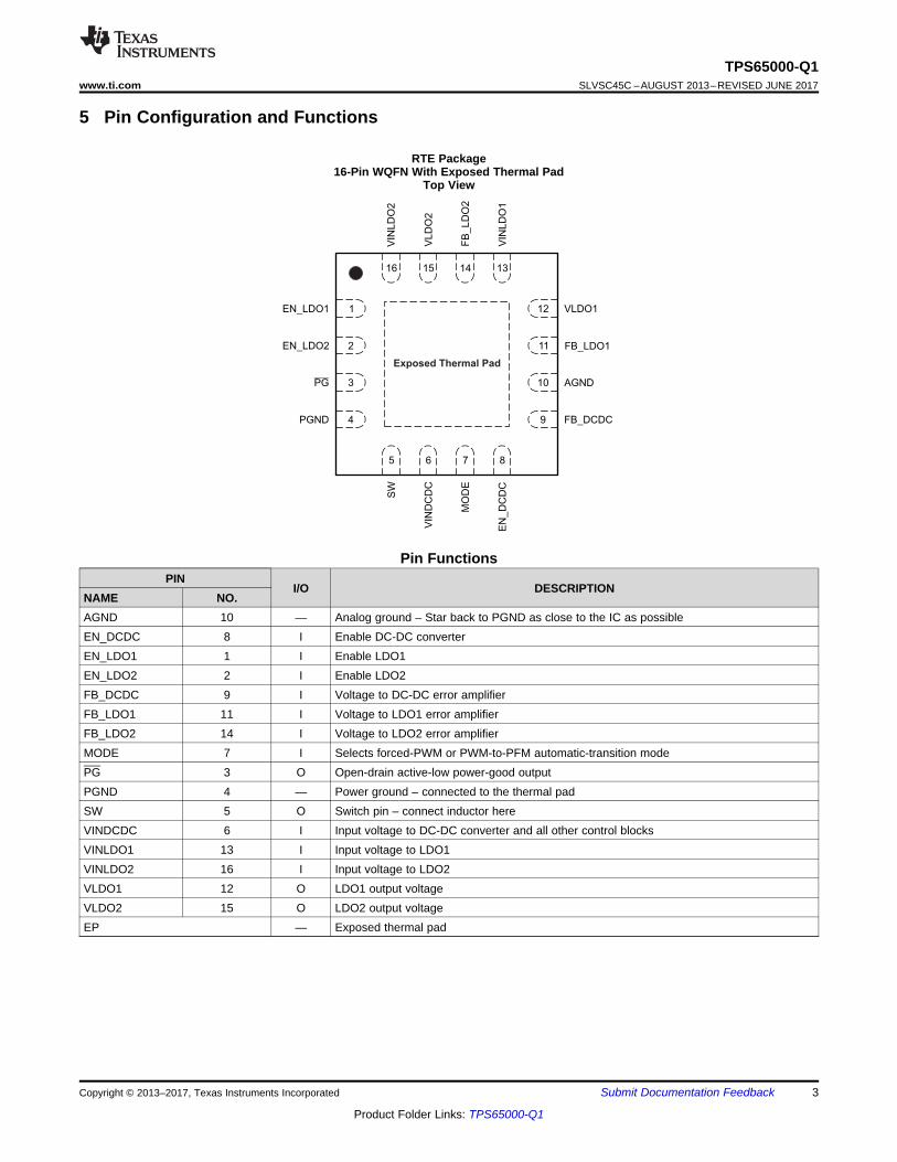
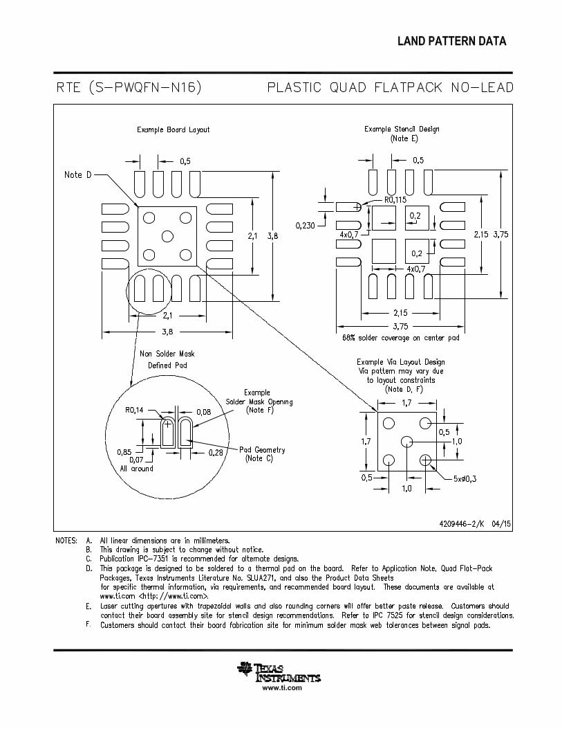
5 Pin Configuration and Functions
RTE Package16-Pin WQFN With Exposed Thermal Pad
Top View
Pin FunctionsPIN
I/O DESCRIPTIONNAME NO.AGND 10 — Analog ground – Star back to PGND as close to the IC as possibleEN_DCDC 8 I Enable DC-DC converterEN_LDO1 1 I Enable LDO1EN_LDO2 2 I Enable LDO2FB_DCDC 9 I Voltage to DC-DC error amplifierFB_LDO1 11 I Voltage to LDO1 error amplifierFB_LDO2 14 I Voltage to LDO2 error amplifierMODE 7 I Selects forced-PWM or PWM-to-PFM automatic-transition modePG 3 O Open-drain active-low power-good outputPGND 4 — Power ground – connected to the thermal padSW 5 O Switch pin – connect inductor hereVINDCDC 6 I Input voltage to DC-DC converter and all other control blocksVINLDO1 13 I Input voltage to LDO1VINLDO2 16 I Input voltage to LDO2VLDO1 12 O LDO1 output voltageVLDO2 15 O LDO2 output voltageEP — Exposed thermal pad

4
TPS65000-Q1SLVSC45C –AUGUST 2013–REVISED JUNE 2017 www.ti.com
Product Folder Links: TPS65000-Q1
Submit Documentation Feedback Copyright © 2013–2017, Texas Instruments Incorporated
(1) Stresses beyond those listed under Absolute Maximum Ratings may cause permanent damage to the device. These are stress ratingsonly, and functional operation of the device at these or any other conditions beyond those indicated under Recommended OperatingConditions is not implied. Exposure to absolute-maximum-rated conditions for extended periods may affect device reliability.
6 Specifications
6.1 Absolute Maximum Ratingsover operating free-air temperature range (unless otherwise noted) (1)
MIN MAX UNIT
Input voltageOn all pins except AGND, PGND, EN_DCDC, VLDO1, VLDO2,FB_LDO1, FB_LDO2, FB_DCDC pins with respect to AGND –0.3 7
VOn EN_DCDC with respect to AGND –0.3 VIN + 0.3, ≤ 7
Output voltage On VLDO1, VLDO2, FB_LDO1, FB_LDO2, FB_DCDC –0.3 3.6 V
CurrentVINDCDC, SW, PGND, 1800 mAVINLDO1, VINLDO2, VLDO1, VLDO1, AGND 800 mAAt all other pins 1 mA
Operating free-air temperature, TA –40 105 °CMaximum junction temperature, TJ 150 °CStorage temperature, Tstg –65 150 °C
(1) AEC Q100-002 indicates HBM stressing is done in accordance with the ANSI/ESDA/JEDEC JS-001 specification.
6.2 ESD RatingsVALUE UNIT
V(ESD)Electrostaticdischarge
Human body model (HBM), per AEC Q100-002 (1) ±2500VCharged device model (CDM), per AEC
Q100-011Corner pins (1, 4, 5, 8, 9, 12, 13, and 16) ±750Other pins ±500
6.3 Recommended Operating ConditionsMIN NOM MAX UNIT
L1 SW pin inductor 1.5 2.2 3.3 μH
CIInput capacitor at VINDCDC 10 μFInput capacitor at VINLDO1, VINLDO2 2.2 μF
COOutput capacitor for VDCDC 10 22 μFOutput capacitor for LDO1, LDO2 2.2 μF
IO
DC-DC converter output current 600 mALDO1 output current 300 mALDO2 output current 300 mA
TA Operating ambient temperature –40 105 °C
5
TPS65000-Q1www.ti.com SLVSC45C –AUGUST 2013–REVISED JUNE 2017
Product Folder Links: TPS65000-Q1
Submit Documentation FeedbackCopyright © 2013–2017, Texas Instruments Incorporated
(1) For more information about traditional and new thermal metrics, see the Semiconductor and IC Package Thermal Metrics applicationreport.
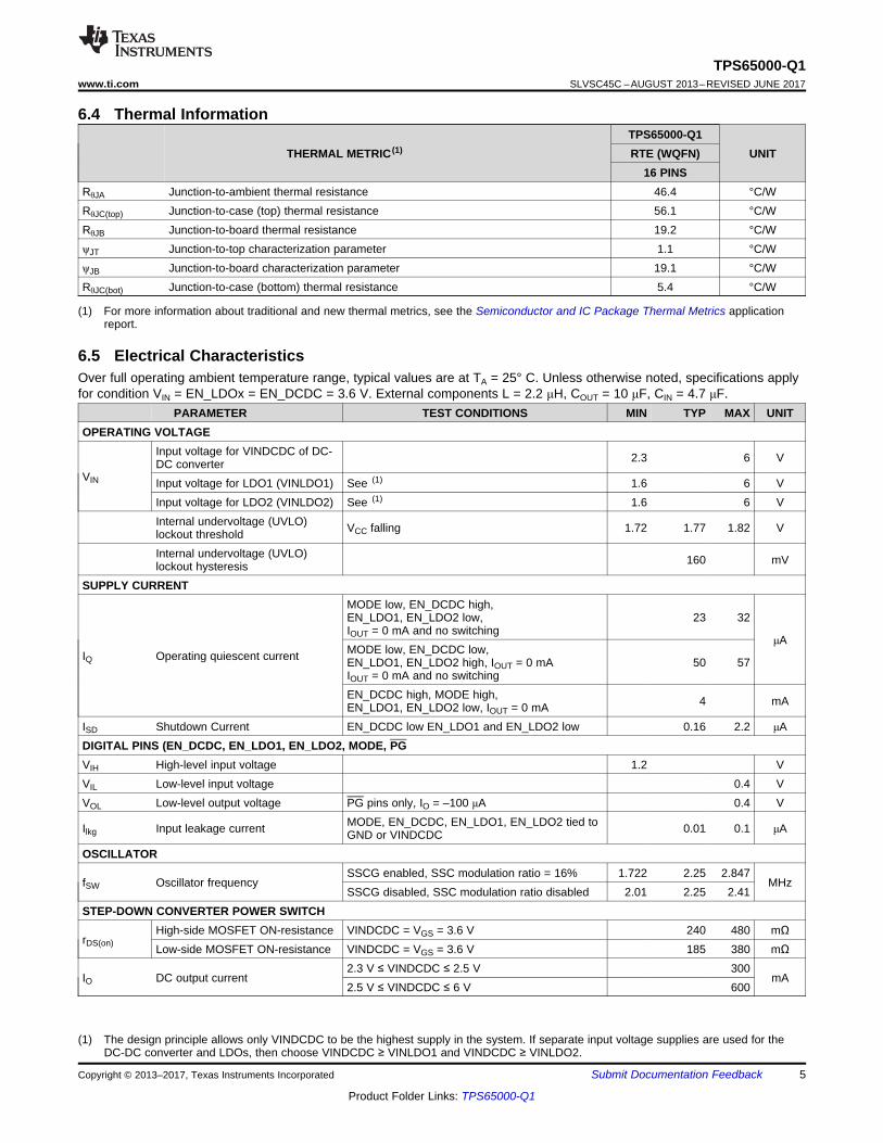
6.4 Thermal Information
THERMAL METRIC (1)TPS65000-Q1
UNITRTE (WQFN)16 PINS
RθJA Junction-to-ambient thermal resistance 46.4 °C/WRθJC(top) Junction-to-case (top) thermal resistance 56.1 °C/WRθJB Junction-to-board thermal resistance 19.2 °C/WψJT Junction-to-top characterization parameter 1.1 °C/WψJB Junction-to-board characterization parameter 19.1 °C/WRθJC(bot) Junction-to-case (bottom) thermal resistance 5.4 °C/W
(1) The design principle allows only VINDCDC to be the highest supply in the system. If separate input voltage supplies are used for theDC-DC converter and LDOs, then choose VINDCDC ≥ VINLDO1 and VINDCDC ≥ VINLDO2.
6.5 Electrical CharacteristicsOver full operating ambient temperature range, typical values are at TA = 25° C. Unless otherwise noted, specifications applyfor condition VIN = EN_LDOx = EN_DCDC = 3.6 V. External components L = 2.2 μH, COUT = 10 μF, CIN = 4.7 μF.
PARAMETER TEST CONDITIONS MIN TYP MAX UNITOPERATING VOLTAGE
VIN
Input voltage for VINDCDC of DC-DC converter 2.3 6 V
Input voltage for LDO1 (VINLDO1) See (1) 1.6 6 VInput voltage for LDO2 (VINLDO2) See (1) 1.6 6 VInternal undervoltage (UVLO)lockout threshold VCC falling 1.72 1.77 1.82 V
Internal undervoltage (UVLO)lockout hysteresis 160 mV
SUPPLY CURRENT
IQ Operating quiescent current
MODE low, EN_DCDC high,EN_LDO1, EN_LDO2 low,IOUT = 0 mA and no switching
23 32
μAMODE low, EN_DCDC low,EN_LDO1, EN_LDO2 high, IOUT = 0 mAIOUT = 0 mA and no switching
50 57
EN_DCDC high, MODE high,EN_LDO1, EN_LDO2 low, IOUT = 0 mA 4 mA
ISD Shutdown Current EN_DCDC low EN_LDO1 and EN_LDO2 low 0.16 2.2 μADIGITAL PINS (EN_DCDC, EN_LDO1, EN_LDO2, MODE, PGVIH High-level input voltage 1.2 VVIL Low-level input voltage 0.4 VVOL Low-level output voltage PG pins only, IO = –100 μA 0.4 V
Ilkg Input leakage current MODE, EN_DCDC, EN_LDO1, EN_LDO2 tied toGND or VINDCDC 0.01 0.1 μA
OSCILLATOR
fSW Oscillator frequencySSCG enabled, SSC modulation ratio = 16% 1.722 2.25 2.847
MHzSSCG disabled, SSC modulation ratio disabled 2.01 2.25 2.41
STEP-DOWN CONVERTER POWER SWITCH
rDS(on)High-side MOSFET ON-resistance VINDCDC = VGS = 3.6 V 240 480 mΩLow-side MOSFET ON-resistance VINDCDC = VGS = 3.6 V 185 380 mΩ
IO DC output current2.3 V ≤ VINDCDC ≤ 2.5 V 300
mA2.5 V ≤ VINDCDC ≤ 6 V 600

6
TPS65000-Q1SLVSC45C –AUGUST 2013–REVISED JUNE 2017 www.ti.com
Product Folder Links: TPS65000-Q1
Submit Documentation Feedback Copyright © 2013–2017, Texas Instruments Incorporated
Electrical Characteristics (continued)Over full operating ambient temperature range, typical values are at TA = 25° C. Unless otherwise noted, specifications applyfor condition VIN = EN_LDOx = EN_DCDC = 3.6 V. External components L = 2.2 μH, COUT = 10 μF, CIN = 4.7 μF.
PARAMETER TEST CONDITIONS MIN TYP MAX UNIT
(2) For VINDCDC = VDCDC + 1 V(3) In PFM mode, the internal reference voltage is typically 1.01 × VREF.(4) Maximum output voltage VLDOx = 3.6 V.(5) VDO = VINLDOx – VLDOx, where VINLDOx = VLDOx(nom) – 100 mV(6) Output voltage specification does not include tolerance of external programming resistors.
ILIMFForward current limit, PMOS andNMOS 2.3 V ≤ VINDCDC ≤ 6 V 800 1000 1400 mA
STEP-DOWN CONVERTER POWER SWITCH (continued)
TSDThermal shutdown Increasing junction temperature 150 °CThermal shutdown hysteresis Decreasing junction temperature 30 °C
STEP-DOWN CONVERTER OUTPUT VOLTAGE
VDCDC Adjustable output voltage range,VDCDC 0.6 VIND
CDC V
FB_DCDC pin current 0.1 μAVref Internal reference voltage 0.594 0.6 0.606 V
VDCDC
Output-voltage accuracy (PWMmode) (2)
MODE = high,2.3 ≤ VINDCDC ≤ 6 V –1.5% 0% 1.5%
Output-voltage accuracy (PFMmode) (3)
MODE low+1% voltage positioning active 1%
Load regulation (PWM mode) MODE high 0.5 %/A
RDISInternal discharge resistance atSW EN_DCDC low 450 Ω
LOW-DROPOUT REGULATORSVI Input voltage for LDOx (VINLDOx) 1.6 6 V
VOAdjustable output voltage, LDOx(VLDOx) (4) 0.73
VINLDOx –VDO
V
IO Continuous-pass FET current 300 mA
ISC Short-circuit current limit2.3 V ≤ VINLDOx 340 700
mAVINLDOx < 2.3 V 210 700
FB_LDOx pin current 0.1 μAFB_LDOx voltage Adjustable VOUT mode only 0.5 V
VDO Dropout voltage (5) VINLDOx ≥ 2.3 V, IOUT = 250 mA 370 mVVINLDOx < 2.3 V, IOUT = 175 mA 370 mV
Output voltage accuracy (6)
IO = 1 mA to 300 mA, VINLDOx = 2.3 V–6 V,VLDOx = 1.2 V –3.5% 3.5%
IO = 1 mA to 175 mA, VINLDOx = 1.6 V–6 V,VLDOx = 1.2 V –3.5% 3.5%
Load regulation IO = 1 mA to 300 mA, VINLDOx = 3.6 VVLDOx = 1.2 V –1.5% 1.5%
Line regulation VINLDOx = 1.6 V–6 V, VLDOx = 1.2 V atIO = 1 mA –0.5% 0.5%
PSRR Power-supply rejection ratio fNOISE ≤ 10 kHz, COUT ≥ 2.2 μF, VIN = 2.3 V,VOUT = 1.3 V, IOUT = 10 mA 40 dB
RDISInternal discharge resistance atVLDOx EN_LDOx low 450 Ω
TSD Thermal shutdown Increasing temperature 150 °CThermal shutdown hysteresis Decreasing temperature 30 °C
t - Time - 2 s/divm
Ch
1:
VD
CD
C1
0m
V/d
iv
Ch
2:
SW
2V
/div
Ch
3:
Lo
ad
Cu
rre
nt
DC
DC
20
mA
div
VINDCDC = 3.6 VT = 25 C
VDCDC = 1.2 VA
o
Load Current = 60mAEN_DCDC = highEN_LDO1 = lowEN_LDO2 = low
t - Time - 200ns/div
Ch1: V
DC
DC
10m
V/d
iv
Ch2: S
W2V
/div
Ch4: Load C
urr
ent
DC
DC
20m
Adiv
VINDCDC = 3.6 VT = 25 C
VDCDC = 1.2 VA
o
Load DCDC = 400mAEN_DCDC = highEN_LDO1 = lowEN_LDO2 = low
0.00001 0.0001 0.001 0.01 0.1 1
IO - Output Current - A
0
50
90
100
Effic
ien
cy -
%
70
40
20
10
VOUT
A
= 1.2V
T = 25 Co
80
60
30
2.3V
2.8V
3.3V
3.6V
4.2V
4.5V
5.5V
5V
6V
0.00001 0.0001 0.001 0.01 0.1 1
IO - Output Current - A
0
50
90
100
Effic
ien
cy -
%
70
40
20
10
80
60
30
VOUT
A
= 1.2V
T = 25 Co
2.3V
2.8V
3.3V
3.6V
4.2V
4.5V
5.5V
5V
6V
7
TPS65000-Q1www.ti.com SLVSC45C –AUGUST 2013–REVISED JUNE 2017
Product Folder Links: TPS65000-Q1
Submit Documentation FeedbackCopyright © 2013–2017, Texas Instruments Incorporated
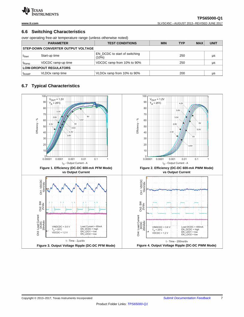
6.6 Switching Characteristicsover operating free-air temperature range (unless otherwise noted)
PARAMETER TEST CONDITIONS MIN TYP MAX UNITSTEP-DOWN CONVERTER OUTPUT VOLTAGE
tStart Start-up time EN_DCDC to start of switching(10%) 250 µs
tRamp VDCDC ramp-up time VDCDC ramp from 10% to 90% 250 µsLOW-DROPOUT REGULATORStRAMP VLDOx ramp time VLDOx ramp from 10% to 90% 200 µs
6.7 Typical Characteristics
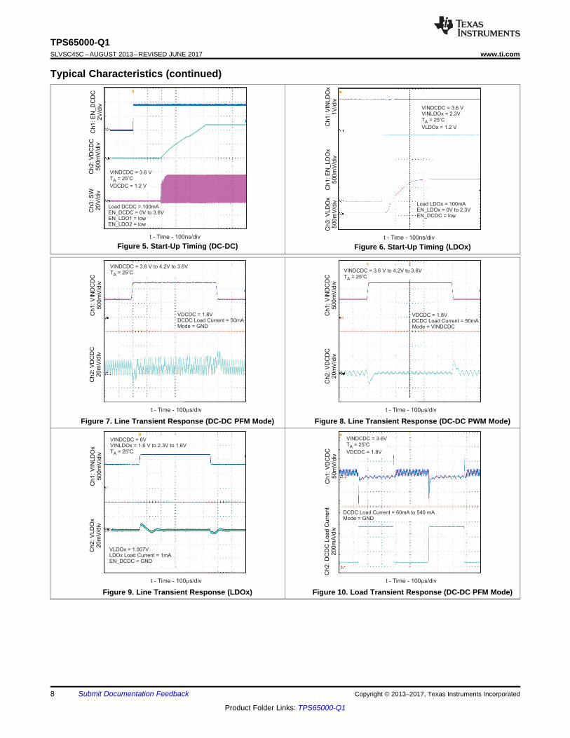
Figure 1. Efficiency (DC-DC 600-mA PFM Mode)vs Output Current
Figure 2. Efficiency (DC-DC 600-mA PWM Mode)vs Output Current
Figure 3. Output Voltage Ripple (DC-DC PFM Mode) Figure 4. Output Voltage Ripple (DC-DC PWM Mode)
t - Time - 100 s/divm
Ch
1:
VIN
LD
Ox
50
0m
V/d
iv
Ch
2:
VL
DO
x2
0m
V/d
iv
VLDOx = 1.007VLDOx Load Current = 1mAEN_DCDC = GND
VINDCDC = 6VVINLDOx = 1.6 V to 2.3V to 1.6V
T = 25 CAo
t - Time - 100 s/divm
Ch
1:
VD
CD
C
50
mV
/div
Ch
2:
DC
DC
Lo
ad
Cu
rre
nt
20
0m
A/d
iv
DCDC Load Current = 60mA to 540 mA
Mode = GND
VINDCDC = 3.6V
T = 25 CA
o
VDCDC = 1.8V
t - Time - 100 s/divm
Ch
1:
VIN
DC
DC
50
0m
V/d
iv
Ch
2:
VD
CD
C
20
mV
/div
VDCDC = 1.8V
DCDC Load Current = 50mA
Mode = GND
VINDCDC = 3.6 V to 4.2V to 3.6V
T = 25 CA
o
t - Time - 100 s/divm
Ch
1:
VIN
DC
DC
50
0m
V/d
iv
Ch
2:
VD
CD
C
20
mV
/div
VDCDC = 1.8V
DCDC Load Current = 50mA
Mode = VINDCDC
VINDCDC = 3.6 V to 4.2V to 3.6V
T = 25 CA
o
t - Time - 100ns/div
Ch
1:
VIN
LD
Ox
1V
/div
Ch
1:
EN
_L
DO
x5
00
mV
/div
Ch
3:
VL
DO
x5
00
mV
/div
VINDCDC = 3.6 VVINLDOx = 2.3V
T = 25 C
VLDOx = 1.2 VA
o
Load LDOx = 100mAEN_LDOx = 0V to 2.3VEN_DCDC = low
t - Time - 100ns/div
Ch
1:
EN
_D
CD
C2
V/d
iv
Ch
2:
VD
CD
C5
00
mV
/div
Ch
3:
SW
20
V/d
iv
VINDCDC = 3.6 V
T = 25 C
VDCDC = 1.2 VA
o
Load DCDC = 100mAEN_DCDC = 0V to 3.6VEN_LDO1 = lowEN_LDO2 = low
8
TPS65000-Q1SLVSC45C –AUGUST 2013–REVISED JUNE 2017 www.ti.com
Product Folder Links: TPS65000-Q1
Submit Documentation Feedback Copyright © 2013–2017, Texas Instruments Incorporated
Typical Characteristics (continued)
Figure 5. Start-Up Timing (DC-DC) Figure 6. Start-Up Timing (LDOx)
Figure 7. Line Transient Response (DC-DC PFM Mode) Figure 8. Line Transient Response (DC-DC PWM Mode)
Figure 9. Line Transient Response (LDOx) Figure 10. Load Transient Response (DC-DC PFM Mode)
10 100 1M 10M
f - Frequency - MHz
0
Re
jectio
n R
atio
- d
B
1k 10k 100k
100
40
90
10
20
30
50
60
70
80
I = 10mAO
V = 2.3V
C = 2.2 F
C = 10 F
IN
O
VLDOx = 1.3V
I m
m
t - Time - 4 s/divm
Ch
1:
Mo
de
2V
/div
Ch
2:
VD
CD
C
20
mV
/div
VINDCDC = 3.6V
DCDC Load Current = 30mA
VDCDC = 1.8V
T = 25 CA
o
Ch
3:
SW
2V
/div
t - Time - 4 s/divm
Ch
1:
Mo
de
2V
/div
Ch
2:
VD
CD
C
20
mV
/div
VINDCDC = 3.6V
T = 25 C
DCDC Load Current = 30mA
VDCDC = 1.8V
A
o
Ch
3:
SW
2V
/div
t - Time - 100 s/divm
Ch
1:
VD
CD
C
50
mV
/div
Ch
2:
DC
DC
Lo
ad
Cu
rre
nt
20
0m
A/d
iv
DCDC Load Current = 60mA to 540 mA
Mode = VINDCDC
VINDCDC = 3.6V
T = 25 C
VDCDC = 1.8V
A
o
t - Time - 200 s/divm
Ch
1:
LD
Ox L
oa
d C
urr
en
t5
0m
A/d
iv
Ch
2:
VL
DO
x2
0m
V/d
iv
VINDCDC = 3.6V
T = 25 C
LDOx
VINLDOx = 3.6V
Load Current = 15mA to 100mAVLDOx = 1.2VEN_DCDC = GND
Ao
9
TPS65000-Q1www.ti.com SLVSC45C –AUGUST 2013–REVISED JUNE 2017
Product Folder Links: TPS65000-Q1
Submit Documentation FeedbackCopyright © 2013–2017, Texas Instruments Incorporated
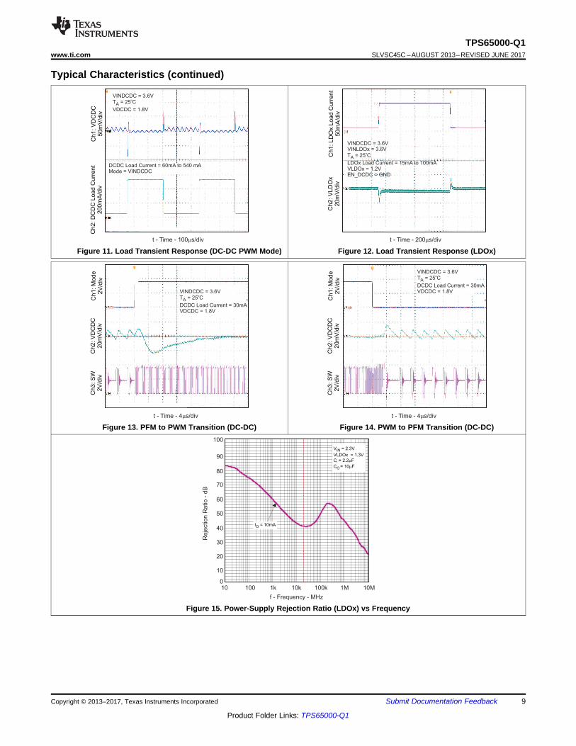
Typical Characteristics (continued)
Figure 11. Load Transient Response (DC-DC PWM Mode) Figure 12. Load Transient Response (LDOx)
Figure 13. PFM to PWM Transition (DC-DC) Figure 14. PWM to PFM Transition (DC-DC)
Figure 15. Power-Supply Rejection Ratio (LDOx) vs Frequency

TPS65000-Q1
VINLDO1
EN_LDO1
VINLDO2
EN_LDO2
VLDO1
VLDO2
AGND
PGND
FB_LDO1
FB_LDO2
Band-Gap Reference
Oscillator
SSCG
3-mm × 3-mm QFN
VINDCDC
EN_DCDC
MODE
SW
FB_DCDC
PG
LDO2
300 mA
Buck Converter
600 mA
LDO1
300 mA
10
TPS65000-Q1SLVSC45C –AUGUST 2013–REVISED JUNE 2017 www.ti.com
Product Folder Links: TPS65000-Q1
Submit Documentation Feedback Copyright © 2013–2017, Texas Instruments Incorporated
7 Detailed Description
7.1 OverviewThe TPS65000-Q1 device provides one step-down converter, two low dropout regulators and spread spectrumclock generation. The device has an input voltage range of2.3 V to 6 V. This device is intended for (but not limited to) powering automotive camera modules.
The output voltage of the step-down converter can be selected through resistor networks on the output. Tomaximize efficiency, there are two modes of operation based on load conditions: PWM or PFM. By pulling theMODE pin high, forced PWM can be achieved. Pulling this pin low results in an automatic adjustment betweenPFM and PWM modes.
The two general-purpose low-dropout regulators each have their own separate enables and voltage inputs. Theinputs can be tied to the output of the step-down converter or to a separate voltage source. Resistor networksare required on the output of the regulator to set the output voltage.
The switching frequency of the step-down converter is handled by the oscillator, with a typical frequency of2.25 MHz. The spread spectrum clock (SSC) modulates this frequency when the device is in PWM mode. Thisadditional circuit in the oscillator block reduces power that may cause EMI.
The TPS65000-Q1 device also provides a power good signal to monitor the condition of the DC-DC and bothLDOs. The DC-DC and LDOs are only monitored if their enable signal is high. If all enabled resources are inregulation, the pin is pulled low. If one or more of the enabled resources are out of regulation, the pin is placed inHi-Z .
7.2 Functional Block Diagram
( )
( )
DC1 DC2DCDC FB_DCDC
DC2
DC1 DC2DCDC
DC2
R + RV = V x
R
R + RV = 0.6V x
R
SWVINDCDC
FB_DCDC
L
CO
RDC2
ZLOAD
EN_DCDC
MODE
VREF(DCDC)+ -
θJA Diode
P
P
A
A
PGNDAGND
PP
Oscillator
DISCHG RDC1CF
Switch Control
11
TPS65000-Q1www.ti.com SLVSC45C –AUGUST 2013–REVISED JUNE 2017
Product Folder Links: TPS65000-Q1
Submit Documentation FeedbackCopyright © 2013–2017, Texas Instruments Incorporated
7.3 Feature Description
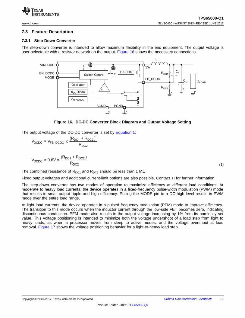
7.3.1 Step-Down ConverterThe step-down converter is intended to allow maximum flexibility in the end equipment. The output voltage isuser-selectable with a resistor network on the output. Figure 16 shows the necessary connections.
Figure 16. DC-DC Converter Block Diagram and Output Voltage Setting
The output voltage of the DC-DC converter is set by Equation 1:
(1)
The combined resistance of RDC1 and RDC2 should be less than 1 MΩ.
Fixed output voltages and additional current-limit options are also possible. Contact TI for further information.
The step-down converter has two modes of operation to maximize efficiency at different load conditions. Atmoderate to heavy load currents, the device operates in a fixed-frequency pulse-width modulation (PWM) modethat results in small output ripple and high efficiency. Pulling the MODE pin to a DC-high level results in PWMmode over the entire load range.
At light load currents, the device operates in a pulsed frequency-modulation (PFM) mode to improve efficiency.The transition to this mode occurs when the inductor current through the low-side FET becomes zero, indicatingdiscontinuous conduction. PFM mode also results in the output voltage increasing by 1% from its nominally setvalue. This voltage positioning is intended to minimize both the voltage undershoot of a load step from light toheavy loads, as when a processor moves from sleep to active modes, and the voltage overshoot at loadremoval. Figure 17 shows the voltage positioning behavior for a light-to-heavy load step.
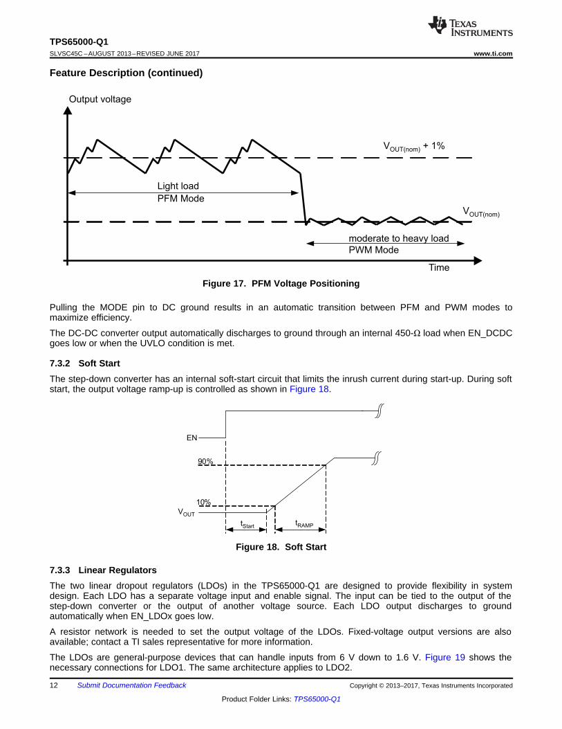
90%
10%
tRAMPt
Start
EN
VOUT
Output voltage
V + 1%OUT(nom)
VOUT(nom)
Light load
PFM Mode
moderate to heavy load
PWM Mode
Time
12
TPS65000-Q1SLVSC45C –AUGUST 2013–REVISED JUNE 2017 www.ti.com
Product Folder Links: TPS65000-Q1
Submit Documentation Feedback Copyright © 2013–2017, Texas Instruments Incorporated
Feature Description (continued)
Figure 17. PFM Voltage Positioning
Pulling the MODE pin to DC ground results in an automatic transition between PFM and PWM modes tomaximize efficiency.
The DC-DC converter output automatically discharges to ground through an internal 450-Ω load when EN_DCDCgoes low or when the UVLO condition is met.
7.3.2 Soft StartThe step-down converter has an internal soft-start circuit that limits the inrush current during start-up. During softstart, the output voltage ramp-up is controlled as shown in Figure 18.
Figure 18. Soft Start
7.3.3 Linear RegulatorsThe two linear dropout regulators (LDOs) in the TPS65000-Q1 are designed to provide flexibility in systemdesign. Each LDO has a separate voltage input and enable signal. The input can be tied to the output of thestep-down converter or the output of another voltage source. Each LDO output discharges to groundautomatically when EN_LDOx goes low.
A resistor network is needed to set the output voltage of the LDOs. Fixed-voltage output versions are alsoavailable; contact a TI sales representative for more information.
The LDOs are general-purpose devices that can handle inputs from 6 V down to 1.6 V. Figure 19 shows thenecessary connections for LDO1. The same architecture applies to LDO2.

( )
( )
LDO1_1 LDO1_2
LDO1 FB_LDO1LDO1_2
LDO1_1 LDO1_2
LDO1LDO1_2
R + RV = V x
R
R + RV = 0.5V x
R
ZLOAD
A
EN_LDO1
VLDO1VINLDO1
FB_LDO1
P
PA
DISCHG
AGND PGND
+ -
θJA Diode
VREF(LD01)
CO(LD01)
RLOD1_2
RLDO1_1
13
TPS65000-Q1www.ti.com SLVSC45C –AUGUST 2013–REVISED JUNE 2017
Product Folder Links: TPS65000-Q1
Submit Documentation FeedbackCopyright © 2013–2017, Texas Instruments Incorporated
Feature Description (continued)
Figure 19. LDO Block Diagram and Output Voltage Setting
The output voltages of the LDOs are set by Equation 2:
(2)
The combined resistance of RLDO1_1 and RLDO1_2 should be less than 1 MΩ.
7.3.4 Oscillator and Spread-Spectrum Clock GenerationThe TPS65000-Q1 contains an internal oscillator running at a typical frequency of 2.25 MHz. This frequency isthe fundamental switching frequency of the step-down converter when it is running in PWM mode. An additionalcircuit in the oscillator block implements spread-spectrum clocking, which modulates the main switchingfrequency when the device is in PWM mode. This spread-spectrum oscillation reduces the power that may causeEMI. When viewed in the frequency domain, the SSC spreads out the frequency that may introduce interferencewhile simultaneously reducing the power. Because the frequency is continually shifting, the amount of time theswitcher spends at any single frequency is reduced. This reduction in time means that the receiver that may seethe interference has less time to integrate the interference.
Different spin versions of SSC settings are also possible; contact a TI sales representative for more information.
Figure 20 and Figure 21 show the advantage of SSC with the frequency spectrum centering on the nominalfrequency 2.25 MHz. The blue spectrum is the result of the spread change. As shown in the figures, theharmonic spectrum is attenuated to 10 dB, compared to the same device without SSC.
EN_DCDC
EN_LDO1
VLDO2
EN_LDO2
PG
A
-
+
VLDO2Target
VLDO1
-
+
VLDO1
Target
VDCDC
-
+
VDCDC
Target
VDCDC
Stop 150 MHz
-20
RBW = 10 kHz
dB
mV
0
-30
10
30
-10
50
20
70
40
60
Start 1.5 MHz Stop 3.5 MHz
-20
RBW = 10 kHz
SSC
ON
SSC
OFF
0
-30
10
30
-10
50
20
70
40
60
Start 1.5 MHz
dB
mV
14
TPS65000-Q1SLVSC45C –AUGUST 2013–REVISED JUNE 2017 www.ti.com
Product Folder Links: TPS65000-Q1
Submit Documentation Feedback Copyright © 2013–2017, Texas Instruments Incorporated
Feature Description (continued)
Figure 20. SSC On and Off Comparison from 1.5 MHz to150 MHz
Figure 21. Zoom In of SSC On and Off Comparison from1.5 MHz to 3.5 MHz
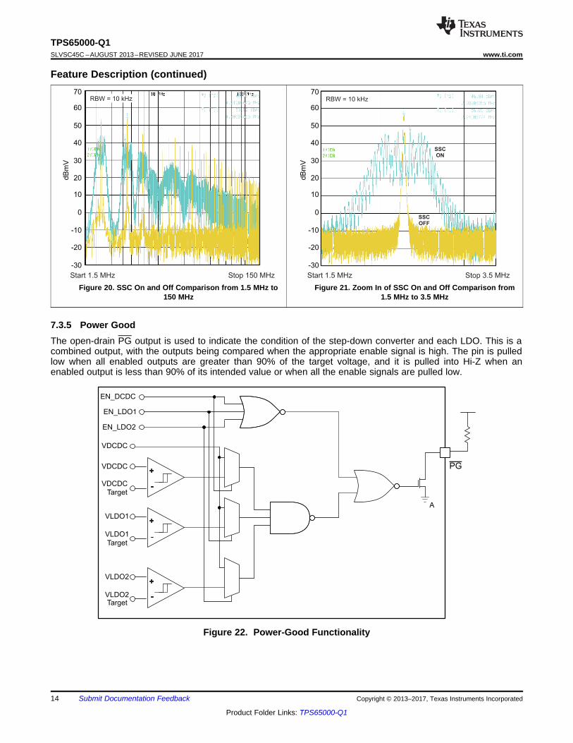
7.3.5 Power GoodThe open-drain PG output is used to indicate the condition of the step-down converter and each LDO. This is acombined output, with the outputs being compared when the appropriate enable signal is high. The pin is pulledlow when all enabled outputs are greater than 90% of the target voltage, and it is pulled into Hi-Z when anenabled output is less than 90% of its intended value or when all the enable signals are pulled low.
Figure 22. Power-Good Functionality

15
TPS65000-Q1www.ti.com SLVSC45C –AUGUST 2013–REVISED JUNE 2017
Product Folder Links: TPS65000-Q1
Submit Documentation FeedbackCopyright © 2013–2017, Texas Instruments Incorporated
7.4 Device Functional ModesThe step-down converter has two modes of operation to maximize efficiency:1. PFM
– For light loads– For automatic transition to between this mode and PWM mode automatically when MODE pin is pulled
low over all load ranges– To increase in output voltage setting by 1%– For better accuracy
2. PWM– For moderate to heavy loads– For a small output ripple– For maintaining the specified switching frequency variation by pulling the MODE pin high which places
the device in a forced PWM mode over the entire load range.
VLDO1
SW
TPS65000-Q1
VINDCDC
VINLDO2
EN_LDO2VDCDC
EN_DCDC
EN_LDO1
VINLDO1
PGNDP
P
P
P
FB_DCDC
PG
MODE
FB_LDO1
AGNDA A
A
A
VLDO2
FB_LDO2
VIN
VLDO1
VLDO22.8V
VIN
10mF
10mF
10mF10 Fm
P
180kW
180kW
820kW
470kW
470kW
680kW
150kW
1.8V
22pF
2.2 Hm
A
VDCDC
3.3V
16
TPS65000-Q1SLVSC45C –AUGUST 2013–REVISED JUNE 2017 www.ti.com
Product Folder Links: TPS65000-Q1
Submit Documentation Feedback Copyright © 2013–2017, Texas Instruments Incorporated
8 Application and Implementation
NOTEInformation in the following applications sections is not part of the TI componentspecification, and TI does not warrant its accuracy or completeness. TI’s customers areresponsible for determining suitability of components for their purposes. Customers shouldvalidate and test their design implementation to confirm system functionality.
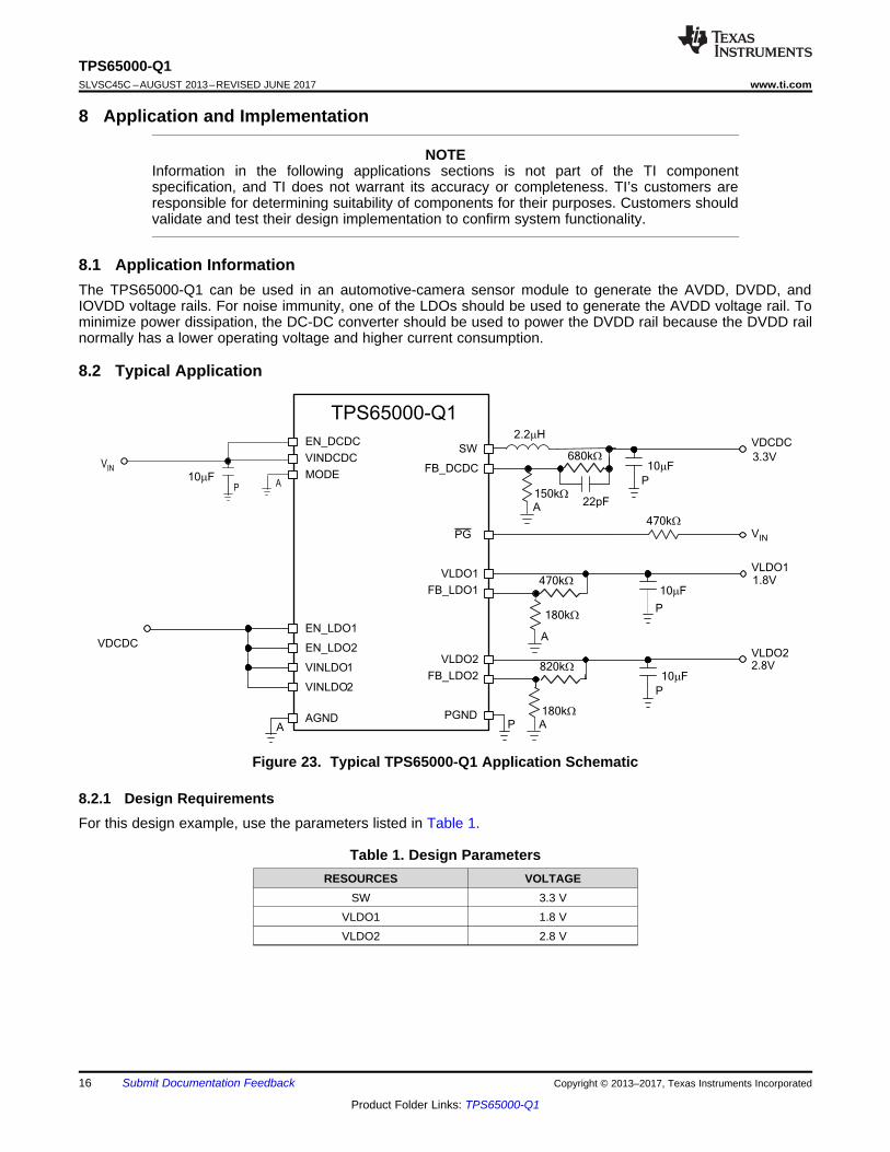
8.1 Application InformationThe TPS65000-Q1 can be used in an automotive-camera sensor module to generate the AVDD, DVDD, andIOVDD voltage rails. For noise immunity, one of the LDOs should be used to generate the AVDD voltage rail. Tominimize power dissipation, the DC-DC converter should be used to power the DVDD rail because the DVDD railnormally has a lower operating voltage and higher current consumption.
8.2 Typical Application
Figure 23. Typical TPS65000-Q1 Application Schematic
8.2.1 Design RequirementsFor this design example, use the parameters listed in Table 1.
Table 1. Design ParametersRESOURCES VOLTAGE
SW 3.3 VVLDO1 1.8 VVLDO2 2.8 V
C
1f OUT
OUT
= with L = 2.2 H, C = 10 F2 L x C
m m
p
LLmax OUTmax
II = I +
2
D
f
OUT
INL OUT
V1 -
VI = V x
L xD
17
TPS65000-Q1www.ti.com SLVSC45C –AUGUST 2013–REVISED JUNE 2017
Product Folder Links: TPS65000-Q1
Submit Documentation FeedbackCopyright © 2013–2017, Texas Instruments Incorporated
8.2.2 Detailed Design Procedure
8.2.2.1 Output Filter Design (Inductor and Output Capacitor)
8.2.2.1.1 Inductor Selection
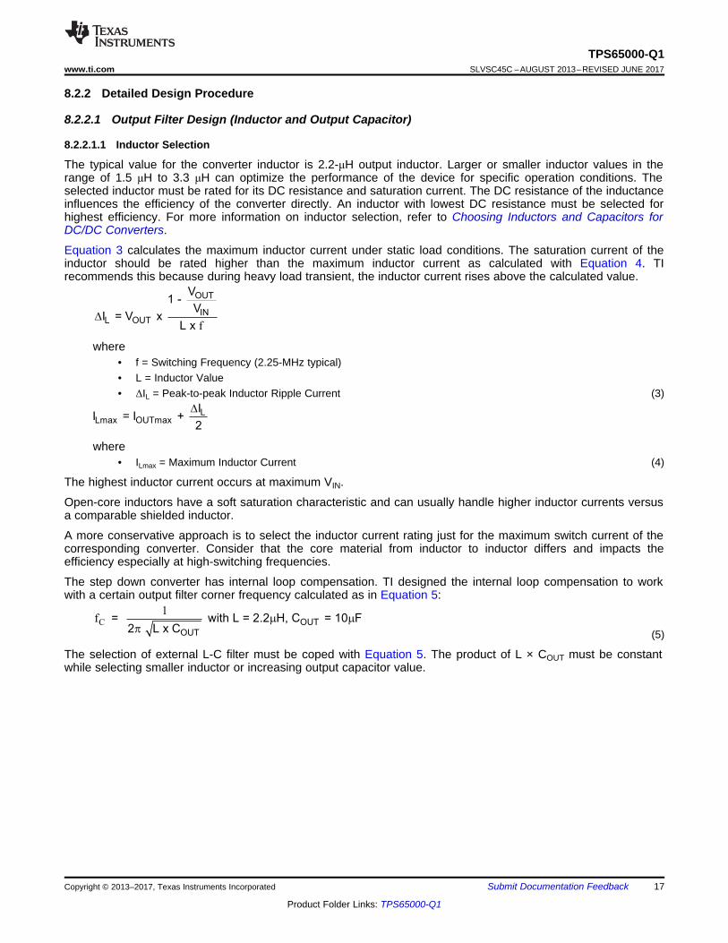
The typical value for the converter inductor is 2.2-μH output inductor. Larger or smaller inductor values in therange of 1.5 μH to 3.3 μH can optimize the performance of the device for specific operation conditions. Theselected inductor must be rated for its DC resistance and saturation current. The DC resistance of the inductanceinfluences the efficiency of the converter directly. An inductor with lowest DC resistance must be selected forhighest efficiency. For more information on inductor selection, refer to Choosing Inductors and Capacitors forDC/DC Converters.
Equation 3 calculates the maximum inductor current under static load conditions. The saturation current of theinductor should be rated higher than the maximum inductor current as calculated with Equation 4. TIrecommends this because during heavy load transient, the inductor current rises above the calculated value.
where• f = Switching Frequency (2.25-MHz typical)• L = Inductor Value• ΔIL = Peak-to-peak Inductor Ripple Current (3)
where• ILmax = Maximum Inductor Current (4)
The highest inductor current occurs at maximum VIN.
Open-core inductors have a soft saturation characteristic and can usually handle higher inductor currents versusa comparable shielded inductor.
A more conservative approach is to select the inductor current rating just for the maximum switch current of thecorresponding converter. Consider that the core material from inductor to inductor differs and impacts theefficiency especially at high-switching frequencies.
The step down converter has internal loop compensation. TI designed the internal loop compensation to workwith a certain output filter corner frequency calculated as in Equation 5:
(5)
The selection of external L-C filter must be coped with Equation 5. The product of L × COUT must be constantwhile selecting smaller inductor or increasing output capacitor value.

f f
OUT
INOUT OUT
OUT
V1 -
V 1V = V x x + ESR
L x 8 x C xD
æ ö÷ç ÷ç ÷ç ÷çè ø
f
OUT
INRMSCout OUT
V1 -
V 1I = V x x
L x 2 x 3
18
TPS65000-Q1SLVSC45C –AUGUST 2013–REVISED JUNE 2017 www.ti.com
Product Folder Links: TPS65000-Q1
Submit Documentation Feedback Copyright © 2013–2017, Texas Instruments Incorporated
8.2.2.1.2 Output Capacitor Selection
The advanced fast response voltage mode control scheme of the converter allows the use of small ceramiccapacitors with a typical value of 22 μF, without having large output voltage under and overshoots during heavyload transients. TI recommends ceramic capacitors with low ESR values because they result in lowest outputvoltage ripple. See for the TI-recommended components.
If ceramic output capacitors are used, the capacitor RMS ripple current rating always meets the applicationrequirements. The RMS ripple current is calculated as in Equation 6:
(6)
At nominal load current, the device operates in PWM mode and the overall output voltage ripple is the sum of thevoltage spike caused by the output capacitor ESR plus the voltage ripple caused by charging and discharging theoutput capacitor as calculated in Equation 7:
(7)
Where the highest output voltage ripple occurs at the highest input voltage VIN.
At light load currents, the converter operates in power save mode and the output voltage ripple is dependent onthe output capacitor value. The output voltage ripple is set by the internal comparator delay and the externalcapacitor. The typical output voltage ripple is less than 1% of the nominal output voltage.
The adjustable output voltage of the DC-DC converter is calculated by Equation 1 in the Step-Down Converter.To keep the external resistor divider network robust against noise, an external feed forward capacitor is requiredfor optimum load transient response. The value of feed forward capacitor must be in the range between 22 pFand 33 pF provided the equivalent resistance of RDC1 || RDC2 in Equation 1 is approximately 300 kΩ. Scalechange on RDC1||RDC2 would apply a scale change to the feed forward capacitor to keep the RC product aconstant.
8.2.2.1.3 Input Capacitor Selection
Due to the DC-DC converter having a pulsating input current, a low-ESR input capacitor is required for best inputvoltage filtering, and minimizing the interference with other circuits caused by high-input voltage spikes . Placethe input capacitor as close as possible to the VINDCDC pin with the clean GND connection. Do the same forthe output capacitor and the inductor. The converters require a ceramic input capacitor of 10 μF. The inputcapacitor can increase without any limit for better input voltage filtering.
t - Time - 100 s/divm
Ch1: V
DC
DC
50m
V/d
iv
Ch2: D
CD
C L
oad C
urr
ent
200m
A/d
iv
DCDC Load Current = 60mA to 540 mA
Mode = VINDCDC
VINDCDC = 3.6V
T = 25 C
VDCDC = 1.8V
A
o
t - Time - 200 s/divm
Ch1: LD
Ox L
oad C
urr
ent
50m
A/d
iv
Ch2: V
LD
Ox
20m
V/d
iv
VINDCDC = 3.6V
T = 25 C
LDOx
VINLDOx = 3.6V
Load Current = 15mA to 100mAVLDOx = 1.2VEN_DCDC = GND
Ao
t - Time - 100 s/divm
Ch1: V
INLD
Ox
500m
V/d
iv
Ch2: V
LD
Ox
20m
V/d
iv
VLDOx = 1.007VLDOx Load Current = 1mAEN_DCDC = GND
VINDCDC = 6VVINLDOx = 1.6 V to 2.3V to 1.6V
T = 25 CAo
t - Time - 100 s/divm
Ch1: V
DC
DC
50m
V/d
iv
Ch2: D
CD
C L
oad C
urr
ent
200m
A/d
iv
DCDC Load Current = 60mA to 540 mA
Mode = GND
VINDCDC = 3.6V
T = 25 CA
o
VDCDC = 1.8V
t - Time - 100 s/divm
Ch1: V
IND
CD
C
500m
V/d
iv
Ch2: V
DC
DC
20m
V/d
iv
VDCDC = 1.8V
DCDC Load Current = 50mA
Mode = GND
VINDCDC = 3.6 V to 4.2V to 3.6V
T = 25 CA
o
t - Time - 100 s/divm
Ch1: V
IND
CD
C
500m
V/d
iv
Ch2: V
DC
DC
20m
V/d
iv
VDCDC = 1.8V
DCDC Load Current = 50mA
Mode = VINDCDC
VINDCDC = 3.6 V to 4.2V to 3.6V
T = 25 CA
o
19
TPS65000-Q1www.ti.com SLVSC45C –AUGUST 2013–REVISED JUNE 2017
Product Folder Links: TPS65000-Q1
Submit Documentation FeedbackCopyright © 2013–2017, Texas Instruments Incorporated
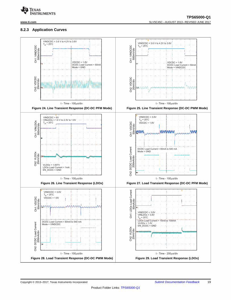
8.2.3 Application Curves
Figure 24. Line Transient Response (DC-DC PFM Mode) Figure 25. Line Transient Response (DC-DC PWM Mode)
Figure 26. Line Transient Response (LDOx) Figure 27. Load Transient Response (DC-DC PFM Mode)
Figure 28. Load Transient Response (DC-DC PWM Mode) Figure 29. Load Transient Response (LDOx)
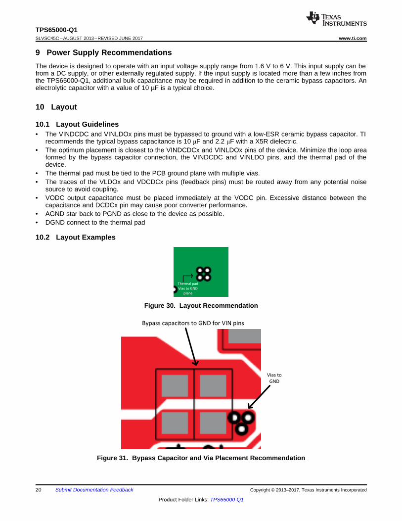
Bypass capacitors to GND for VIN pins
Vias to
GND
Thermal pad
Vias to GND
plane
20
TPS65000-Q1SLVSC45C –AUGUST 2013–REVISED JUNE 2017 www.ti.com
Product Folder Links: TPS65000-Q1
Submit Documentation Feedback Copyright © 2013–2017, Texas Instruments Incorporated
9 Power Supply RecommendationsThe device is designed to operate with an input voltage supply range from 1.6 V to 6 V. This input supply can befrom a DC supply, or other externally regulated supply. If the input supply is located more than a few inches fromthe TPS65000-Q1, additional bulk capacitance may be required in addition to the ceramic bypass capacitors. Anelectrolytic capacitor with a value of 10 µF is a typical choice.
10 Layout
10.1 Layout Guidelines• The VINDCDC and VINLDOx pins must be bypassed to ground with a low-ESR ceramic bypass capacitor. TI
recommends the typical bypass capacitance is 10 μF and 2.2 μF with a X5R dielectric.• The optimum placement is closest to the VINDCDCx and VINLDOx pins of the device. Minimize the loop area
formed by the bypass capacitor connection, the VINDCDC and VINLDO pins, and the thermal pad of thedevice.
• The thermal pad must be tied to the PCB ground plane with multiple vias.• The traces of the VLDOx and VDCDCx pins (feedback pins) must be routed away from any potential noise
source to avoid coupling.• VODC output capacitance must be placed immediately at the VODC pin. Excessive distance between the
capacitance and DCDCx pin may cause poor converter performance.• AGND star back to PGND as close to the device as possible.• DGND connect to the thermal pad
10.2 Layout Examples
Figure 30. Layout Recommendation
Figure 31. Bypass Capacitor and Via Placement Recommendation

21
TPS65000-Q1www.ti.com SLVSC45C –AUGUST 2013–REVISED JUNE 2017
Product Folder Links: TPS65000-Q1
Submit Documentation FeedbackCopyright © 2013–2017, Texas Instruments Incorporated
11 Device and Documentation Support
11.1 Device Support
11.1.1 Third-Party Products DisclaimerTI'S PUBLICATION OF INFORMATION REGARDING THIRD-PARTY PRODUCTS OR SERVICES DOES NOTCONSTITUTE AN ENDORSEMENT REGARDING THE SUITABILITY OF SUCH PRODUCTS OR SERVICESOR A WARRANTY, REPRESENTATION OR ENDORSEMENT OF SUCH PRODUCTS OR SERVICES, EITHERALONE OR IN COMBINATION WITH ANY TI PRODUCT OR SERVICE.
11.2 Documentation Support
11.2.1 Related DocumentationFor related documentation, see the following:
Choosing Inductors and Capacitors for DC/DC Converters
11.3 Receiving Notification of Documentation UpdatesTo receive notification of documentation updates, navigate to the device product folder on ti.com. In the upperright corner, click on Alert me to register and receive a weekly digest of any product information that haschanged. For change details, review the revision history included in any revised document.
11.4 Community ResourcesThe following links connect to TI community resources. Linked contents are provided "AS IS" by the respectivecontributors. They do not constitute TI specifications and do not necessarily reflect TI's views; see TI's Terms ofUse.
TI E2E™ Online Community TI's Engineer-to-Engineer (E2E) Community. Created to foster collaborationamong engineers. At e2e.ti.com, you can ask questions, share knowledge, explore ideas and helpsolve problems with fellow engineers.
Design Support TI's Design Support Quickly find helpful E2E forums along with design support tools andcontact information for technical support.
11.5 TrademarksE2E is a trademark of Texas Instruments.All other trademarks are the property of their respective owners.
11.6 Electrostatic Discharge CautionThis integrated circuit can be damaged by ESD. Texas Instruments recommends that all integrated circuits be handled withappropriate precautions. Failure to observe proper handling and installation procedures can cause damage.
ESD damage can range from subtle performance degradation to complete device failure. Precision integrated circuits may be moresusceptible to damage because very small parametric changes could cause the device not to meet its published specifications.
11.7 GlossarySLYZ022 — TI Glossary.
This glossary lists and explains terms, acronyms, and definitions.
12 Mechanical, Packaging, and Orderable InformationThe following pages include mechanical, packaging, and orderable information. This information is the mostcurrent data available for the designated devices. This data is subject to change without notice and revision ofthis document. For browser-based versions of this data sheet, refer to the left-hand navigation.
PACKAGE OPTION ADDENDUM
www.ti.com 10-Dec-2020
Addendum-Page 1
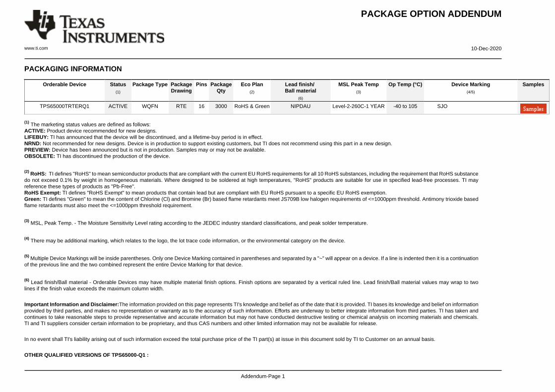
PACKAGING INFORMATION
Orderable Device Status(1)
Package Type PackageDrawing
Pins PackageQty
Eco Plan(2)
Lead finish/Ball material
(6)
MSL Peak Temp(3)
Op Temp (°C) Device Marking(4/5)
Samples
TPS65000TRTERQ1 ACTIVE WQFN RTE 16 3000 RoHS & Green NIPDAU Level-2-260C-1 YEAR -40 to 105 SJO
(1) The marketing status values are defined as follows:ACTIVE: Product device recommended for new designs.LIFEBUY: TI has announced that the device will be discontinued, and a lifetime-buy period is in effect.NRND: Not recommended for new designs. Device is in production to support existing customers, but TI does not recommend using this part in a new design.PREVIEW: Device has been announced but is not in production. Samples may or may not be available.OBSOLETE: TI has discontinued the production of the device.
(2) RoHS: TI defines "RoHS" to mean semiconductor products that are compliant with the current EU RoHS requirements for all 10 RoHS substances, including the requirement that RoHS substancedo not exceed 0.1% by weight in homogeneous materials. Where designed to be soldered at high temperatures, "RoHS" products are suitable for use in specified lead-free processes. TI mayreference these types of products as "Pb-Free".RoHS Exempt: TI defines "RoHS Exempt" to mean products that contain lead but are compliant with EU RoHS pursuant to a specific EU RoHS exemption.Green: TI defines "Green" to mean the content of Chlorine (Cl) and Bromine (Br) based flame retardants meet JS709B low halogen requirements of <=1000ppm threshold. Antimony trioxide basedflame retardants must also meet the <=1000ppm threshold requirement.
(3) MSL, Peak Temp. - The Moisture Sensitivity Level rating according to the JEDEC industry standard classifications, and peak solder temperature.
(4) There may be additional marking, which relates to the logo, the lot trace code information, or the environmental category on the device.
(5) Multiple Device Markings will be inside parentheses. Only one Device Marking contained in parentheses and separated by a "~" will appear on a device. If a line is indented then it is a continuationof the previous line and the two combined represent the entire Device Marking for that device.
(6) Lead finish/Ball material - Orderable Devices may have multiple material finish options. Finish options are separated by a vertical ruled line. Lead finish/Ball material values may wrap to twolines if the finish value exceeds the maximum column width.
Important Information and Disclaimer:The information provided on this page represents TI's knowledge and belief as of the date that it is provided. TI bases its knowledge and belief on informationprovided by third parties, and makes no representation or warranty as to the accuracy of such information. Efforts are underway to better integrate information from third parties. TI has taken andcontinues to take reasonable steps to provide representative and accurate information but may not have conducted destructive testing or chemical analysis on incoming materials and chemicals.TI and TI suppliers consider certain information to be proprietary, and thus CAS numbers and other limited information may not be available for release.
In no event shall TI's liability arising out of such information exceed the total purchase price of the TI part(s) at issue in this document sold by TI to Customer on an annual basis.
OTHER QUALIFIED VERSIONS OF TPS65000-Q1 :
PACKAGE OPTION ADDENDUM
www.ti.com 10-Dec-2020
Addendum-Page 2
• Catalog: TPS65000
NOTE: Qualified Version Definitions:
• Catalog - TI's standard catalog product

TAPE AND REEL INFORMATION
*All dimensions are nominal
Device PackageType
PackageDrawing
Pins SPQ ReelDiameter
(mm)
ReelWidth
W1 (mm)
A0(mm)
B0(mm)
K0(mm)
P1(mm)
W(mm)
Pin1Quadrant
TPS65000TRTERQ1 WQFN RTE 16 3000 330.0 12.4 3.3 3.3 1.1 8.0 12.0 Q2
PACKAGE MATERIALS INFORMATION
www.ti.com 31-May-2018
Pack Materials-Page 1
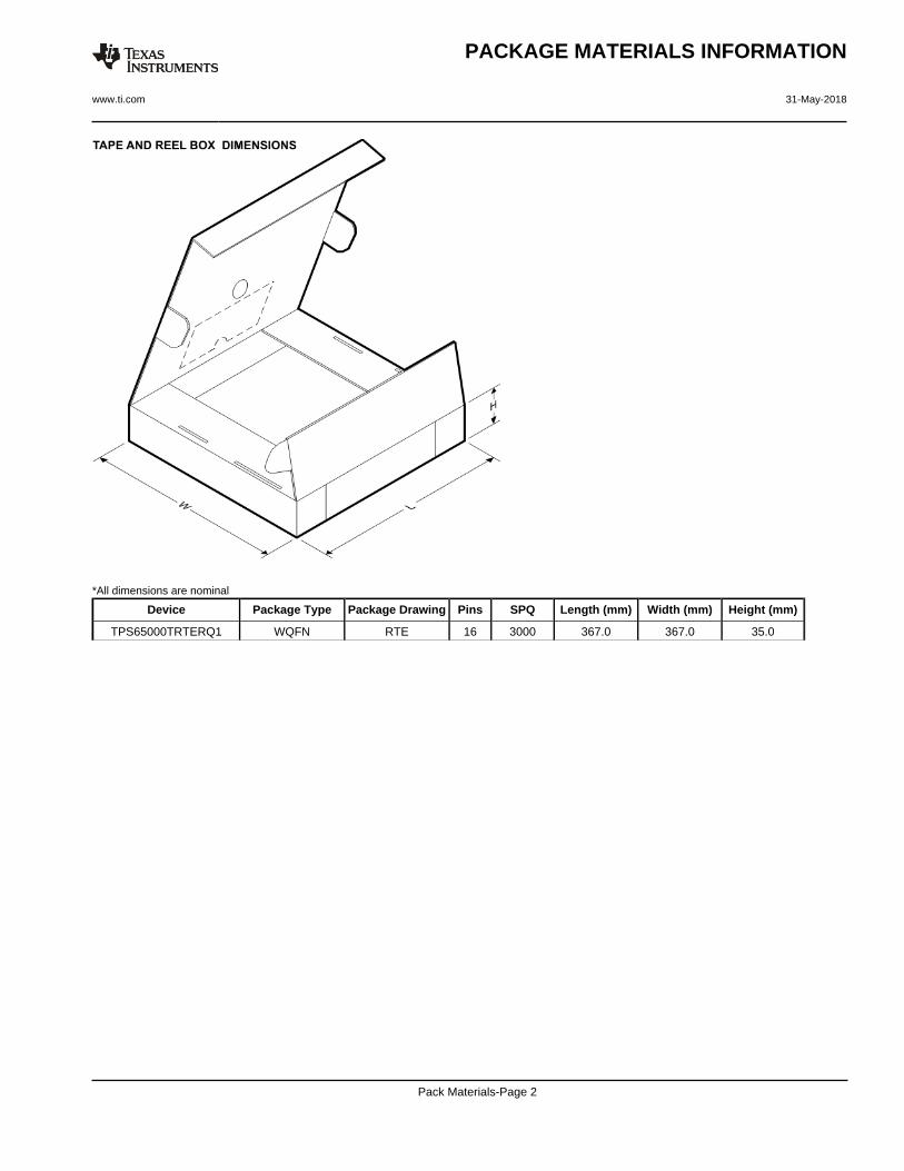
*All dimensions are nominal
Device Package Type Package Drawing Pins SPQ Length (mm) Width (mm) Height (mm)
TPS65000TRTERQ1 WQFN RTE 16 3000 367.0 367.0 35.0
PACKAGE MATERIALS INFORMATION
www.ti.com 31-May-2018
Pack Materials-Page 2


IMPORTANT NOTICE AND DISCLAIMER
TI PROVIDES TECHNICAL AND RELIABILITY DATA (INCLUDING DATASHEETS), DESIGN RESOURCES (INCLUDING REFERENCE DESIGNS), APPLICATION OR OTHER DESIGN ADVICE, WEB TOOLS, SAFETY INFORMATION, AND OTHER RESOURCES “AS IS” AND WITH ALL FAULTS, AND DISCLAIMS ALL WARRANTIES, EXPRESS AND IMPLIED, INCLUDING WITHOUT LIMITATION ANY IMPLIED WARRANTIES OF MERCHANTABILITY, FITNESS FOR A PARTICULAR PURPOSE OR NON-INFRINGEMENT OF THIRD PARTY INTELLECTUAL PROPERTY RIGHTS.These resources are intended for skilled developers designing with TI products. You are solely responsible for (1) selecting the appropriate TI products for your application, (2) designing, validating and testing your application, and (3) ensuring your application meets applicable standards, and any other safety, security, or other requirements. These resources are subject to change without notice. TI grants you permission to use these resources only for development of an application that uses the TI products described in the resource. Other reproduction and display of these resources is prohibited. No license is granted to any other TI intellectual property right or to any third party intellectual property right. TI disclaims responsibility for, and you will fully indemnify TI and its representatives against, any claims, damages, costs, losses, and liabilities arising out of your use of these resources.TI’s products are provided subject to TI’s Terms of Sale (www.ti.com/legal/termsofsale.html) or other applicable terms available either on ti.com or provided in conjunction with such TI products. TI’s provision of these resources does not expand or otherwise alter TI’s applicable warranties or warranty disclaimers for TI products.
Mailing Address: Texas Instruments, Post Office Box 655303, Dallas, Texas 75265Copyright © 2020, Texas Instruments Incorporated