tps56320x 4.5-v to 17-v input, 3-a synchronous step … 3 4 5 6 v out v out en c out v in c in vbst...
TRANSCRIPT
Output Current (A)
Effi
cien
cy
0.001 0.005 0.02 0.05 0.1 0.2 0.5 1 2 310%
20%
30%
40%
50%
60%
70%
80%
90%
100%
D023
VOUT = 1.05 VVOUT = 1.5 VVOUT = 1.8 VVOUT = 3.3 VVOUT = 5 V
TPS563201
VIN
SW
GND1
2
3 4
5
6
VOUT
VOUT
EN
VINCOUT
CIN
VBST
EN
VFB
Product
Folder
Sample &Buy
Technical
Documents
Tools &
Software
Support &Community
TPS563201, TPS563208SLVSD90 –DECEMBER 2015
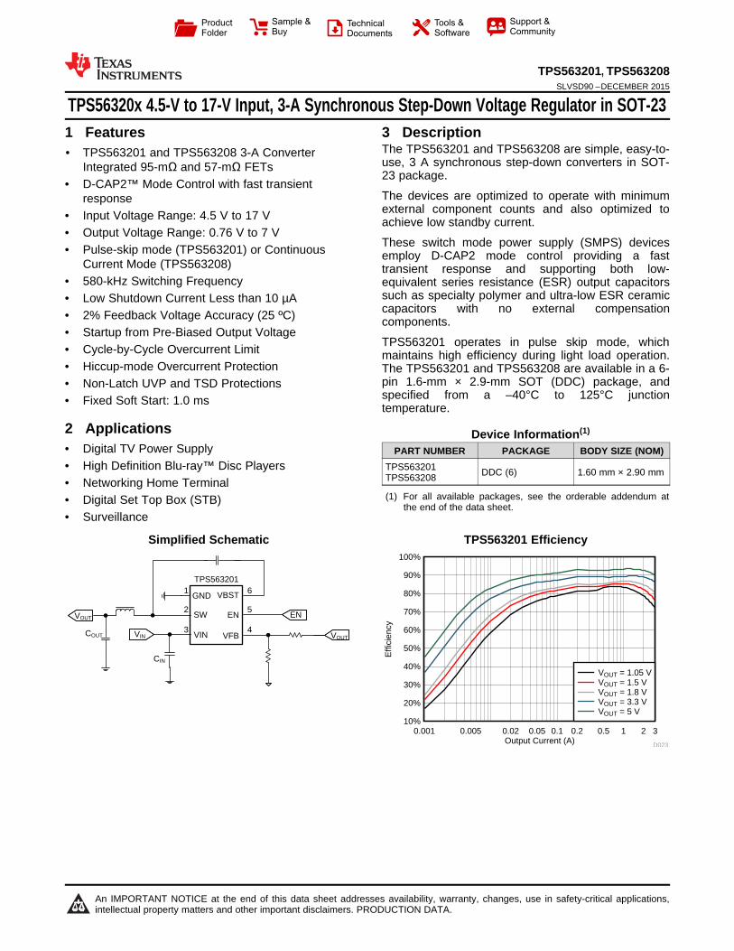
TPS56320x 4.5-V to 17-V Input, 3-A Synchronous Step-Down Voltage Regulator in SOT-231 Features 3 Description
The TPS563201 and TPS563208 are simple, easy-to-1• TPS563201 and TPS563208 3-A Converter
use, 3 A synchronous step-down converters in SOT-Integrated 95-mΩ and 57-mΩ FETs23 package.
• D-CAP2™ Mode Control with fast transientThe devices are optimized to operate with minimumresponseexternal component counts and also optimized to• Input Voltage Range: 4.5 V to 17 V achieve low standby current.
• Output Voltage Range: 0.76 V to 7 VThese switch mode power supply (SMPS) devices• Pulse-skip mode (TPS563201) or Continuous employ D-CAP2 mode control providing a fast
Current Mode (TPS563208) transient response and supporting both low-• 580-kHz Switching Frequency equivalent series resistance (ESR) output capacitors
such as specialty polymer and ultra-low ESR ceramic• Low Shutdown Current Less than 10 µAcapacitors with no external compensation• 2% Feedback Voltage Accuracy (25 ºC) components.
• Startup from Pre-Biased Output VoltageTPS563201 operates in pulse skip mode, which• Cycle-by-Cycle Overcurrent Limit maintains high efficiency during light load operation.
• Hiccup-mode Overcurrent Protection The TPS563201 and TPS563208 are available in a 6-pin 1.6-mm × 2.9-mm SOT (DDC) package, and• Non-Latch UVP and TSD Protectionsspecified from a –40°C to 125°C junction• Fixed Soft Start: 1.0 ms temperature.
2 Applications Device Information(1)
• Digital TV Power Supply PART NUMBER PACKAGE BODY SIZE (NOM)• High Definition Blu-ray™ Disc Players TPS563201 DDC (6) 1.60 mm × 2.90 mmTPS563208• Networking Home Terminal
(1) For all available packages, see the orderable addendum at• Digital Set Top Box (STB)the end of the data sheet.
• Surveillance
Simplified Schematic TPS563201 Efficiency
1
An IMPORTANT NOTICE at the end of this data sheet addresses availability, warranty, changes, use in safety-critical applications,intellectual property matters and other important disclaimers. PRODUCTION DATA.
TPS563201, TPS563208SLVSD90 –DECEMBER 2015 www.ti.com
Table of Contents7.4 Device Functional Modes........................................ 111 Features .................................................................. 1
8 Application and Implementation ........................ 122 Applications ........................................................... 18.1 Application Information............................................ 123 Description ............................................................. 18.2 Typical Application ................................................. 124 Revision History..................................................... 2
9 Power Supply Recommendations ...................... 175 Pin Configuration and Functions ......................... 310 Layout................................................................... 176 Specifications......................................................... 3
10.1 Layout Guidelines ................................................. 176.1 Absolute Maximum Ratings ...................................... 310.2 Layout Example .................................................... 186.2 ESD Ratings.............................................................. 3
11 Device and Documentation Support ................. 196.3 Recommended Operating Conditions....................... 411.1 Related Links ........................................................ 196.4 Thermal Information .................................................. 411.2 Community Resources.......................................... 196.5 Electrical Characteristics........................................... 511.3 Trademarks ........................................................... 196.6 Typical Characteristics .............................................. 611.4 Electrostatic Discharge Caution............................ 197 Detailed Description .............................................. 911.5 Glossary ................................................................ 197.1 Overview ................................................................... 9
12 Mechanical, Packaging, and Orderable7.2 Functional Block Diagram ......................................... 9Information ........................................................... 197.3 Feature Description................................................... 9
4 Revision History
DATE REVISION NOTESDecember 2015 * Initial release.
2 Submit Documentation Feedback Copyright © 2015, Texas Instruments Incorporated
Product Folder Links: TPS563201 TPS563208

GND 1 VBST6
SW 2 EN5
VIN 3 VFB4
TPS563201, TPS563208www.ti.com SLVSD90 –DECEMBER 2015
5 Pin Configuration and Functions
DDC Package6-Pin SOTTop View
Pin FunctionsPIN
I/O DESCRIPTIONNAME NO.
Ground pin Source terminal of low-side power NFET as well as the ground terminal forGND 1 — controller circuit. Connect sensitive VFB to this GND at a single point.SW 2 O Switch node connection between high-side NFET and low-side NFET.VIN 3 I Input voltage supply pin. The drain terminal of high-side power NFET.VFB 4 I Converter feedback input. Connect to output voltage with feedback resistor divider.EN 5 I Enable input control. Active high and must be pulled up to enable the device.
Supply input for the high-side NFET gate drive circuit. Connect 0.1 µF capacitor betweenVBST 6 O VBST and SW pins.
6 Specifications
6.1 Absolute Maximum Ratingsover operating free-air temperature range (unless otherwise noted) (1)
MIN MAX UNITVIN, EN –0.3 19 VVBST –0.3 25 VVBST (10 ns transient) –0.3 27 V
Input voltage VBST (vs SW) –0.3 6.5 VVFB –0.3 6.5 VSW –2 19 VSW (10 ns transient) –3.5 21 V
Operating junction temperature, TJ –40 150 °CStorage temperature, Tstg –55 150 °C
(1) Stresses beyond those listed under Absolute Maximum Ratings may cause permanent damage to the device. These are stress ratingsonly, which do not imply functional operation of the device at these or any other conditions beyond those indicated under RecommendedOperating Conditions. Exposure to absolute-maximum-rated conditions for extended periods may affect device reliability.
6.2 ESD RatingsVALUE UNIT
Human-body model (HBM), per ANSI/ESDA/JEDEC JS-001 (1) ±3000V(ESD) Electrostatic discharge VCharged-device model (CDM), per JEDEC specification JESD22- ±1500C101 (2)
(1) JEDEC document JEP155 states that 500-V HBM allows safe manufacturing with a standard ESD control process.(2) JEDEC document JEP157 states that 250-V CDM allows safe manufacturing with a standard ESD control process.
Copyright © 2015, Texas Instruments Incorporated Submit Documentation Feedback 3
Product Folder Links: TPS563201 TPS563208

TPS563201, TPS563208SLVSD90 –DECEMBER 2015 www.ti.com
6.3 Recommended Operating Conditionsover operating free-air temperature range (unless otherwise noted)
MIN NOM MAX UNITVIN Supply input voltage range 4.5 17 V
VBST –0.1 23VBST (10 ns transient) –0.1 26VBST (vs SW) –0.1 6.0
VI Input voltage range EN –0.1 17 VVFB –0.1 5.5SW –1.8 17SW (10 ns transient) –3.5 20
TJ Operating junction temperature –40 125 °C
6.4 Thermal InformationTPS56320x
THERMAL METRIC (1) DDC (SOT) UNIT6 PINS
RθJA Junction-to-ambient thermal resistance 92.6 °C/WRθJC(top) Junction-to-case (top) thermal resistance 48.5 °C/WRθJB Junction-to-board thermal resistance 15.5 °C/WψJT Junction-to-top characterization parameter 2.5 °C/WψJB Junction-to-board characterization parameter 15.5 °C/W
(1) For more information about traditional and new thermal metrics, see the Semiconductor and IC Package Thermal Metrics applicationreport, SPRA953.
4 Submit Documentation Feedback Copyright © 2015, Texas Instruments Incorporated
Product Folder Links: TPS563201 TPS563208

TPS563201, TPS563208www.ti.com SLVSD90 –DECEMBER 2015
6.5 Electrical CharacteristicsTJ = –40°C to 125°C, VIN = 12 V (unless otherwise noted)
PARAMETER TEST CONDITIONS MIN TYP MAX UNITSUPPLY CURRENT
TPS563201 380 520Operating – non-switchingIVIN VIN current, EN = 5 V, VFB = 0.8 V µAsupply current TPS563208 590 750IVINSDN Shutdown supply current VIN current, EN = 0 V 1 10 µALOGIC THRESHOLDVENH EN high-level input voltage EN 1.6 VVENL EN low-level input voltage EN 0.8 VREN EN pin resistance to GND VEN = 12 V 225 400 900 kΩVFB VOLTAGE AND DISCHARGE RESISTANCE
VFB threshold voltage VO = 1.05 V, IO = 10 mA, Eco-mode™ operation 774 mVVFBTH VFB threshold voltage VO = 1.05 V, continuous mode operation 749 768 787 mVIVFB VFB input current VFB = 0.8 V 0 ±0.1 µAMOSFETRDS(on)h High-side switch resistance TA = 25°C, VBST – SW = 5.5 V 95 mΩRDS(on)l Low-side switch resistance TA = 25°C 57 mΩCURRENT LIMITIocl Current limit DC current, VOUT = 1.05 V, L1 = 1.5 µH 3.3 4.2 5.1 ATHERMAL SHUTDOWN
Shutdown temperature 172Thermal shutdownTSDN °Cthreshold (1) Hysteresis 37ON-TIME TIMER CONTROLtOFF(MIN) Minimum off time VFB = 0.5 V 220 310 nsSOFT STARTTss Soft-start time Internal soft-start time 1.0 msFREQUENCYFsw Switching frequency VIN = 12 V, VO = 1.05 V, FCCM mode 580 kHzOUTPUT UNDERVOLTAGE AND OVERVOLTAGE PROTECTIONVUVP Output UVP threshold Hiccup detect (H > L) 65%THICCUP_WAIT Hiccup on time 1.8 msTHICCUP_RE Hiccup time before restart 15 msUVLO
Wake up VIN voltage 4.0 4.3UVLO UVLO threshold Shutdown VIN voltage 3.3 3.6 V
Hysteresis VIN voltage 0.4
(1) Not production tested.
Copyright © 2015, Texas Instruments Incorporated Submit Documentation Feedback 5
Product Folder Links: TPS563201 TPS563208

Junction Temperature (qC)
Hig
h-S
ide
Rds
_on
(m:
)
-40 -20 0 20 40 60 80 100 120 14050
70
90
110
130
150
170
D005 Junction Temperature (qC)
Low
Sid
e R
ds_o
n (m:
)
-40 -20 0 20 40 60 80 100 120 14030
40
50
60
70
80
90
100
D006
Junction Temperature (qC)
EN
Pin
UV
LO -
Low
(V
)
-40 -20 0 20 40 60 80 100 120 1401.02
1.05
1.08
1.11
1.14
1.17
1.2
1.23
D003 Junction Temperature (qC)
EN
Pin
UV
LO -
Hig
h (V
)
-40 -20 0 20 40 60 80 100 120 1401.35
1.38
1.41
1.44
1.47
1.5
D004
Junction Temperature (qC)
Buc
k Q
uies
cent
Cur
rent
(m
A)
-40 -20 0 20 40 60 80 100 120 1400.3
0.35
0.4
0.45
0.5
0.55
0.6
D001 Junction Temperature (qC)
FB
Vol
tage
(V
)
-40 -20 0 20 40 60 80 100 120 1400.759
0.76
0.761
0.762
0.763
0.764
D002
TPS563201, TPS563208SLVSD90 –DECEMBER 2015 www.ti.com
6.6 Typical CharacteristicsVIN = 12 V (unless otherwise noted)
Figure 1. TPS563201 Supply Current vs Junction Figure 2. VFB Voltage vs Junction TemperatureTemperature
Figure 3. EN Pin UVLO Low Voltage vs Junction Figure 4. EN Pin UVLO High Voltage vs JunctionTemperature Temperature
Figure 5. High-Side Rds-On vs Junction Temperature Figure 6. Low-Side Rds-On vs Junction Temperature
6 Submit Documentation Feedback Copyright © 2015, Texas Instruments Incorporated
Product Folder Links: TPS563201 TPS563208

Output Current (A)
Effi
cien
cy
0.001 0.005 0.02 0.05 0.1 0.2 0.5 1 2 310%
20%
30%
40%
50%
60%
70%
80%
90%
100%
D011
VIN = 5 VVIN = 9 VVIN = 12 VVIN = 15 V
Output Current (A)
Effi
cien
cy
0.001 0.005 0.02 0.05 0.1 0.2 0.5 1 2 310%
20%
30%
40%
50%
60%
70%
80%
90%
100%
D012
VIN = 5 VVIN = 9 VVIN = 12 VVIN = 15 V
Output Current (A)
Effi
cien
cy
0.001 0.005 0.02 0.05 0.1 0.2 0.5 1 2 310%
20%
30%
40%
50%
60%
70%
80%
90%
100%
D009
VIN = 5 VVIN = 9 VVIN = 12 VVIN = 15 V
Output Current (A)
Effi
cien
cy
0.001 0.005 0.02 0.05 0.1 0.2 0.5 1 2 310%
20%
30%
40%
50%
60%
70%
80%
90%
100%
D010
VIN = 5 VVIN = 9 VVIN = 12 VVIN = 15 V
Input Voltage (V)
Sw
itchi
ng F
requ
ency
(kH
z)
4 6 8 10 12 14 16 18500
520
540
560
580
600
620
D007
VOUT = 1.8 VVOUT = 3.3 VVOUT = 5 V
Output Current (A)
Sw
itchi
ng F
requ
ency
(kH
z)
0.001 0.005 0.02 0.05 0.1 0.2 0.5 1 2 30
100
200
300
400
500
600
D008
VOUT = 1.05 VVOUT = 3.3 VVOUT = 5 V
TPS563201, TPS563208www.ti.com SLVSD90 –DECEMBER 2015
Typical Characteristics (continued)VIN = 12 V (unless otherwise noted)
IOUT = 10 mA VIN = 12 V
Figure 7. TPS563208 Switching Frequency vs Input Voltage Figure 8. TPS563201 Switching Frequency vs OutputCurrent
Figure 9. TPS563201 VOUT = 1.05 V Efficiency, L = 2.2 µH Figure 10. TPS563201 VOUT = 1.5 V Efficiency, L = 2.2 µH
Figure 11. TPS563201 VOUT = 1.8 V Efficiency, L = 2.2 µH Figure 12. TPS563201 VOUT = 3.3 V Efficiency, L = 2.2 µH
Copyright © 2015, Texas Instruments Incorporated Submit Documentation Feedback 7
Product Folder Links: TPS563201 TPS563208

Output Current (A)
Effi
cien
cy
0.001 0.005 0.02 0.05 0.1 0.2 0.5 1 2 30
10%
20%
30%
40%
50%
60%
70%
80%
90%
100%
D017
VIN = 5 VVIN = 9 VVIN = 12 VVIN = 15 V
Output Current (A)
Effi
cien
cy
0.001 0.005 0.02 0.05 0.1 0.2 0.5 1 2 30
10%
20%
30%
40%
50%
60%
70%
80%
90%
100%
D018
VIN = 9 VVIN = 12 VVIN = 15 V
Output Current (A)
Effi
cien
cy
0.001 0.005 0.02 0.05 0.1 0.2 0.5 1 2 30
10%
20%
30%
40%
50%
60%
70%
80%
90%
100%
D015
VIN = 5 VVIN = 9 VVIN = 12 VVIN = 15 V
Output Current (A)
Effi
cien
cy
0.001 0.005 0.02 0.05 0.1 0.2 0.5 1 2 30
10%
20%
30%
40%
50%
60%
70%
80%
90%
100%
D016
VIN = 5 VVIN = 9 VVIN = 12 VVIN = 15 V
Output Current (A)
Effi
cien
cy
0.001 0.005 0.02 0.05 0.1 0.2 0.5 1 2 310%
20%
30%
40%
50%
60%
70%
80%
90%
100%
D013
VIN = 9 VVIN = 12 VVIN = 15 V
Output Current (A)
Effi
cien
cy
0.001 0.005 0.02 0.05 0.1 0.2 0.5 1 2 30
10%
20%
30%
40%
50%
60%
70%
80%
90%
100%
D014
VIN = 5 VVIN = 9 VVIN = 12 VVIN = 15 V
TPS563201, TPS563208SLVSD90 –DECEMBER 2015 www.ti.com
Typical Characteristics (continued)VIN = 12 V (unless otherwise noted)
Figure 13. TPS563201 VOUT = 5 V Efficiency, L = 3.3 µH Figure 14. TPS563208 VOUT = 1.05 V Efficiency, L = 2.2 µH
Figure 15. TPS563208 VOUT = 1.5 V Efficiency, L = 2.2 µH Figure 16. TPS563208 VOUT = 1.8 V Efficiency, L = 2.2 µH
Figure 17. TPS563208 VOUT = 3.3 V Efficiency, L = 2.2 µH Figure 18. TPS563208 VOUT = 5 V Efficiency, L = 3.3 µH
8 Submit Documentation Feedback Copyright © 2015, Texas Instruments Incorporated
Product Folder Links: TPS563201 TPS563208

2 SW
ZC
PWM
Control Logic +
+
+
UVP
OVP
3 VIN
tON
One-Shot
6 VBST
+
4VFB
OCL+
+
Soft Start
5EN
HS
LS
1 GND
SS
VoltageReference
Ref
HiccupVUVP
OCLThreshold
Regulator
UVLO
VREG5
VREG5TSD
VOVP
±
±
±
±
±
XCON
TPS563201, TPS563208www.ti.com SLVSD90 –DECEMBER 2015
7 Detailed Description
7.1 OverviewThe TPS563201 and TPS563208 are 3-A synchronous step-down converters. The proprietary D-CAP2 modecontrol supports low ESR output capacitors such as specialty polymer capacitors and multi-layer ceramiccapacitors without complex external compensation circuits. The fast transient response of D-CAP2 mode controlcan reduce the output capacitance required to meet a specific level of performance.
7.2 Functional Block Diagram
7.3 Feature Description
7.3.1 Adaptive On-Time Control and PWM OperationThe main control loop of the TPS563201 and TPS563208 is adaptive on-time pulse width modulation (PWM)controller that supports a proprietary D-CAP2 mode control. The D-CAP2 mode control combines adaptive on-time control with an internal compensation circuit for pseudo-fixed frequency and low external component countconfiguration with both low-ESR and ceramic output capacitors. It is stable even with virtually no ripple at theoutput.
At the beginning of each cycle, the high-side MOSFET is turned on. This MOSFET is turned off after internal oneshot timer expires. This one shot duration is set proportional to the converter input voltage, VIN, and inverselyproportional to the output voltage, VO, to maintain a pseudo-fixed frequency over the input voltage range, henceit is called adaptive on-time control. The one-shot timer is reset and the high-side MOSFET is turned on againwhen the feedback voltage falls below the reference voltage. An internal ramp is added to reference voltage tosimulate output ripple, eliminating the need for ESR induced output ripple from D-CAP2 mode control.
Copyright © 2015, Texas Instruments Incorporated Submit Documentation Feedback 9
Product Folder Links: TPS563201 TPS563208

IN OUT OUTOUT(LL)
SW IN
(V V ) V1I
2 L f V
u u
u u
TPS563201, TPS563208SLVSD90 –DECEMBER 2015 www.ti.com
Feature Description (continued)7.3.2 Pulse Skip Control (TPS563201)The TPS563201 is designed with advanced Eco-mode to maintain high light load efficiency. As the output currentdecreases from heavy load condition, the inductor current is also reduced and eventually comes to point that itsrippled valley touches zero level, which is the boundary between continuous conduction and discontinuousconduction modes. The rectifying MOSFET is turned off when the zero inductor current is detected. As the loadcurrent further decreases the converter runs into discontinuous conduction mode. The on-time is kept almost thesame as it was in the continuous conduction mode so that it takes longer time to discharge the output capacitorwith smaller load current to the level of the reference voltage. This makes the switching frequency lower,proportional to the load current, and keeps the light load efficiency high. The transition point to the light loadoperation IOUT(LL) current can be calculated in Equation 1.
(1)
7.3.3 Soft Start and Pre-Biased Soft StartThe TPS563201 and TPS563208 have an internal 1-ms soft-start. When the EN pin becomes high, the internalsoft-start function begins ramping up the reference voltage to the PWM comparator.
If the output capacitor is pre-biased at startup, the devices initiate switching and start ramping up only after theinternal reference voltage becomes greater than the feedback voltage VFB. This scheme ensures that theconverters ramp up smoothly into regulation point.
7.3.4 Current ProtectionThe output over-current limit (OCL) is implemented using a cycle-by-cycle valley detect control circuit. The switchcurrent is monitored during the OFF state by measuring the low-side FET drain to source voltage. This voltage isproportional to the switch current. To improve accuracy, the voltage sensing is temperature compensated.
During the on time of the high-side FET switch, the switch current increases at a linear rate determined by Vin,Vout, the on-time and the output inductor value. During the on time of the low-side FET switch, this currentdecreases linearly. The average value of the switch current is the load current Iout. If the monitored current isabove the OCL level, the converter maintains low-side FET on and delays the creation of a new set pulse, eventhe voltage feedback loop requires one, until the current level becomes OCL level or lower. In subsequentswitching cycles, the on-time is set to a fixed value and the current is monitored in the same manner.
There are some important considerations for this type of over-current protection. The load current is higher thanthe over-current threshold by one half of the peak-to-peak inductor ripple current. Also, when the current is beinglimited, the output voltage tends to fall as the demanded load current may be higher than the current availablefrom the converter. This may cause the output voltage to fall. When the VFB voltage falls below the UVPthreshold voltage, the UVP comparator detects it. And then, the device will shut down after the UVP delay time(typically 24 µs) and re-start after the hiccup time (typically 15 ms).
When the over current condition is removed, the output voltage returns to the regulated value.
7.3.5 Undervoltage Lockout (UVLO) ProtectionUVLO protection monitors the internal regulator voltage. When the voltage is lower than UVLO threshold voltage,the device is shut off. This protection is non-latching.
7.3.6 Thermal ShutdownThe device monitors the temperature of itself. If the temperature exceeds the threshold value (typically 172°C),the device is shut off. This is a non-latch protection.
10 Submit Documentation Feedback Copyright © 2015, Texas Instruments Incorporated
Product Folder Links: TPS563201 TPS563208

TPS563201, TPS563208www.ti.com SLVSD90 –DECEMBER 2015
7.4 Device Functional Modes
7.4.1 Normal OperationWhen the input voltage is above the UVLO threshold and the EN voltage is above the enable threshold, theTPS563201 and TPS563208 can operate in their normal switching modes. Normal continuous conduction mode(CCM) occurs when the minimum switch current is above 0 A. In CCM, the TPS563201 and TPS563208 operateat a quasi-fixed frequency of 580 kHz.
7.4.2 Eco-mode OperationWhen the TPS563201 and TPS563208 are in the normal CCM operating mode and the switch current falls to 0A, the TPS563201 and TPS563208 begin operating in pulse skipping Eco-mode. Each switching cycle isfollowed by a period of energy saving sleep time. The sleep time ends when the VFB voltage falls below the Eco-mode threshold voltage. As the output current decreases, the perceived time between switching pulsesincreases.
7.4.3 Standby OperationWhen the TPS563201 and TPS563208 are operating in either normal CCM or Eco-mode, they may be placed instandby by asserting the EN pin low.
Copyright © 2015, Texas Instruments Incorporated Submit Documentation Feedback 11
Product Folder Links: TPS563201 TPS563208
1
L1
R210 k
R1 3.09 k
VIN = 4.5 V to 17 V
VOUT
2.2 H
C4
R3 10 k
C7 0.1 F
C822 F
VOUT
C922 F
VIN
Not Installed
EN
VIN
VBST
SW
GND
EN
VFB
1
2
3 4
5
6
1
1
C30.1 F
C210 F
C110 F
VOUT = 1.05 V/3A
TPS563201, TPS563208SLVSD90 –DECEMBER 2015 www.ti.com
8 Application and Implementation
NOTEInformation in the following applications sections is not part of the TI componentspecification, and TI does not warrant its accuracy or completeness. TI’s customers areresponsible for determining suitability of components for their purposes. Customers shouldvalidate and test their design implementation to confirm system functionality.
8.1 Application InformationThe devices are typical step-down DC-DC converters. It typically uses to convert a higher dc voltage to a lowerdc voltage with a maximum available output current of 3 A. The following design procedure can be used to selectcomponent values for the TPS563201 and TPS563208. Alternately, the WEBENCH® software may be used togenerate a complete design. The WEBENCH software uses an iterative design procedure and accesses acomprehensive database of components when generating a design. This section presents a simplified discussionof the design process.
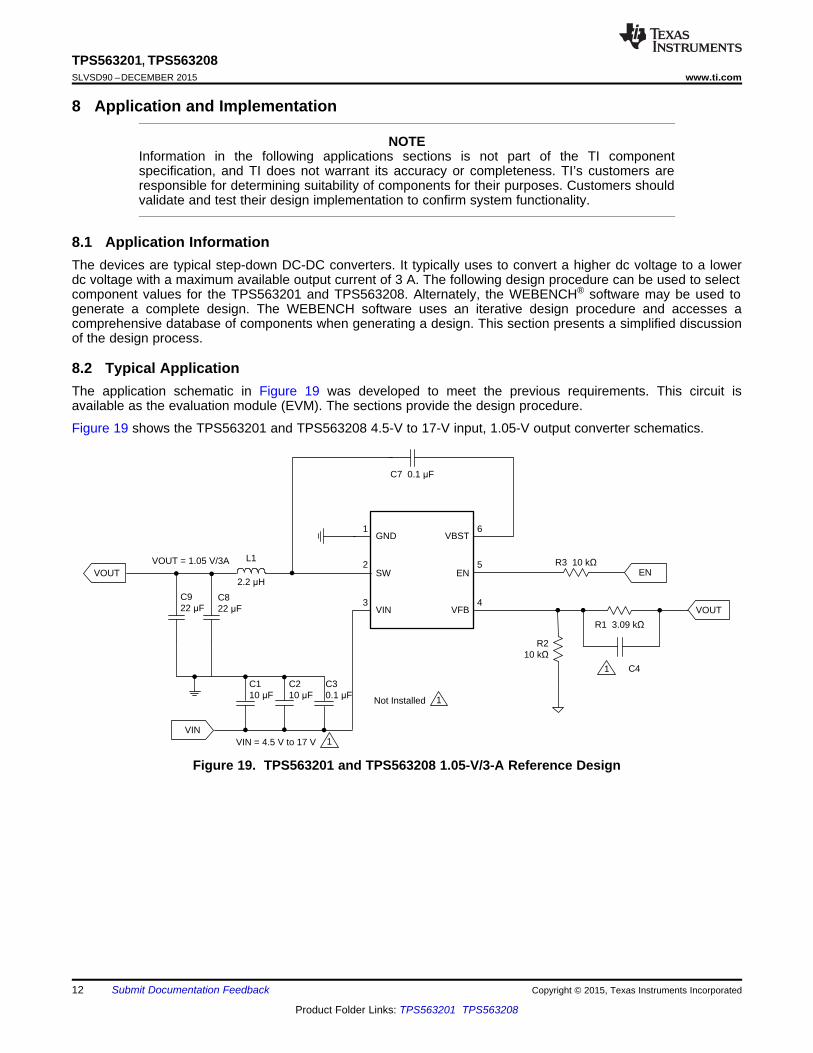
8.2 Typical ApplicationThe application schematic in Figure 19 was developed to meet the previous requirements. This circuit isavailable as the evaluation module (EVM). The sections provide the design procedure.
Figure 19 shows the TPS563201 and TPS563208 4.5-V to 17-V input, 1.05-V output converter schematics.
Figure 19. TPS563201 and TPS563208 1.05-V/3-A Reference Design
12 Submit Documentation Feedback Copyright © 2015, Texas Instruments Incorporated
Product Folder Links: TPS563201 TPS563208

POUT OUT
1f
2 L C
S u
OUTR1
V 0.768 1R2
§ · u ¨ ¸
© ¹
TPS563201, TPS563208www.ti.com SLVSD90 –DECEMBER 2015
Typical Application (continued)8.2.1 Design RequirementsTable 1 shows the design parameters for this application.
Table 1. Design ParametersPARAMETER EXAMPLE VALUE
Input voltage range 4.5 to 17 VOutput voltage 1.05 VTransient response, 1.5-A load step ΔVout = ±5%Input ripple voltage 400 mVOutput ripple voltage 30 mVOutput current rating 3 AOperating frequency 580 kHz
8.2.2 Detailed Design Procedure
8.2.2.1 Output Voltage Resistors SelectionThe output voltage is set with a resistor divider from the output node to the VFB pin. TI recommends to use 1%tolerance or better divider resistors. Start by using Equation 2 to calculate VOUT.
To improve efficiency at very light loads consider using larger value resistors, too high of resistance will be moresusceptible to noise and voltage errors from the VFB input current will be more noticeable.
(2)
8.2.2.2 Output Filter SelectionThe LC filter used as the output filter has double pole at:
(3)
At low frequencies, the overall loop gain is set by the output set-point resistor divider network and the internalgain of the device. The low frequency phase is 180°. At the output filter pole frequency, the gain rolls off at a –40dB per decade rate and the phase drops rapidly. D-CAP2 introduces a high frequency zero that reduces the gainroll off to –20 dB per decade and increases the phase to 90° one decade above the zero frequency. The inductorand capacitor for the output filter must be selected so that the double pole of Equation 3 is located below thehigh frequency zero but close enough that the phase boost provided be the high frequency zero providesadequate phase margin for a stable circuit. To meet this requirement use the values recommended in Table 2.
Table 2. Recommended Component ValuesL1 (µH)OUTPUT R1 (kΩ) R2 (kΩ) C8 + C9 (µF)VOLTAGE (V) MIN TYP MAX
1 3.09 10.0 1.5 2.2 4.7 20 to 681.05 3.74 10.0 1.5 2.2 4.7 20 to 681.2 5.76 10.0 1.5 2.2 4.7 20 to 681.5 9.53 10.0 1.5 2.2 4.7 20 to 681.8 13.7 10.0 1.5 2.2 4.7 20 to 682.5 22.6 10.0 2.2 2.2 4.7 20 to 683.3 33.2 10.0 2.2 2.2 4.7 20 to 685 54.9 10.0 3.3 3.3 4.7 20 to 68
6.5 75 10.0 3.3 3.3 4.7 20 to 68
Copyright © 2015, Texas Instruments Incorporated Submit Documentation Feedback 13
Product Folder Links: TPS563201 TPS563208

Output Current (A)
Out
put V
olta
ge (
V)
0 0.5 1 1.5 2 2.5 3-3%
-2%
-1%
0
1%
2%
3%
D019
TPS563201TPS563208
Output Current (A)
Out
put V
olta
ge (
V)
0 0.5 1 1.5 2 2.5 3-3%
-2%
-1%
0
1%
2%
3%
D020
TPS563201TPS563208
OUT IN OUTCO(RMS)
IN O SW
V V VI
12 V L f
u
u u u
2 2LO(RMS) O P P
1I I Il
12
P PPEAK O
IlIl I
2
IN(MAX) OUTOUTP P
IN(MAX) O SW
V VVIl
V L f
u
u
TPS563201, TPS563208SLVSD90 –DECEMBER 2015 www.ti.com
The inductor peak-to-peak ripple current, peak current and RMS current are calculated using Equation 4,Equation 5, and Equation 6. The inductor saturation current rating must be greater than the calculated peakcurrent and the RMS or heating current rating must be greater than the calculated RMS current.
(4)
(5)
(6)
For this design example, the calculated peak current is 3.5 A and the calculated RMS current is 3.01 A. Theinductor used is a WE 74431122 with a peak current rating of 13 A and an RMS current rating of 9 A.
The capacitor value and ESR determines the amount of output voltage ripple. The TPS563201 and TPS563208are intended for use with ceramic or other low ESR capacitors. Recommended values range from 20 µF to 68µF. Use Equation 7 to determine the required RMS current rating for the output capacitor.
(7)
For this design two TDK C3216X5R0J226M 22-µF output capacitors are used. The typical ESR is 2 mΩ each.The calculated RMS current is 0.286 A and each output capacitor is rated for 4 A.
8.2.2.3 Input Capacitor SelectionThe TPS563201 and TPS563208 require an input decoupling capacitor and a bulk capacitor is neededdepending on the application. TI recommends a ceramic capacitor over 10 µF for the decoupling capacitor. Anadditional 0.1-µF capacitor (C3) from pin 3 to ground is optional to provide additional high frequency filtering. Thecapacitor voltage rating needs to be greater than the maximum input voltage.
8.2.2.4 Bootstrap Capacitor SelectionA 0.1-µF ceramic capacitor must be connected between the VBST to SW pin for proper operation. TIrecommends to use a ceramic capacitor.
8.2.3 Application Curves
Figure 20. TPS563201 and TPS563208 Load Regulation, Figure 21. TPS563201 and TPS563208 Load Regulation,VIN = 5 V VIN = 12 V
14 Submit Documentation Feedback Copyright © 2015, Texas Instruments Incorporated
Product Folder Links: TPS563201 TPS563208

VOUT = 20 mV/div
LX = 5 V/div
IL = 500 mA/div
VOUT = 20 mV/div LX = 5 V/div
IL = 2 A/div
VIN = 100 mV/div
LX = 5 V/div
IOUT = 2 A/div
VOUT = 100 mV/div
LX = 5 V/div
IL = 500 mA/div
Input Voltage (V)
Out
put V
olta
ge (
V)
4 6 8 10 12 14 16 181.047
1.048
1.049
1.05
1.051
1.052
1.053
1.054
1.055
D021
TPS563201TPS563208
Output Current (A)
Effi
cien
cy
0.001 0.005 0.02 0.05 0.1 0.2 0.5 1 2 310%
20%
30%
40%
50%
60%
70%
80%
90%
100%
D022
VIN = 5 VVIN = 9 VVIN = 12 VVIN = 15 V
TPS563201, TPS563208www.ti.com SLVSD90 –DECEMBER 2015
IOUT of TPS563201: 1 AIOUT of TPS563208: 10 mA
Figure 22. TPS563201 and TPS563208 Line Regulation Figure 23. TPS563201 Efficiency
800 ns/div 20 µs/div
Figure 24. TPS563201 Input Voltage Ripple Figure 25. TPS563201 Output Voltage Ripple, 10 mA
1 µs/div 1 µs/div
Figure 26. TPS563201 Output Voltage Ripple, Iout = 0.25 A Figure 27. TPS563201 Output Voltage Ripple, Iout = 2 A
Copyright © 2015, Texas Instruments Incorporated Submit Documentation Feedback 15
Product Folder Links: TPS563201 TPS563208
VEN = 5 V/div
VOUT = 500 mV/div
VIN = 5 V/div
VEN = 5 V/div
VOUT = 500 mV/div
VIN = 5 V/div
VOUT = 20 mV/div
IOUT = 1 A/div
IOUT = 1 A/div
VOUT = 20 mV/div
VOUT = 50 mV/div
IOUT = 1 A/div
VOUT = 10 mV/div
SW = 5 V/div
TPS563201, TPS563208SLVSD90 –DECEMBER 2015 www.ti.com
800 ns/div 100 µs/div
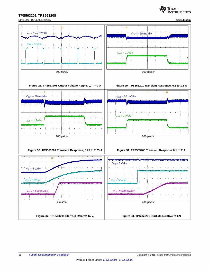
Figure 28. TPS563208 Output Voltage Ripple, IOUT = 0 A Figure 29. TPS563201 Transient Response, 0.1 to 1.5 A
100 µs/div 100 µs/div
Figure 30. TPS563201 Transient Response, 0.75 to 2.25 A Figure 31. TPS563208 Transient Response 0.1 to 2 A
2 ms/div 400 µs/div
Figure 32. TPS563201 Start Up Relative to VI Figure 33. TPS563201 Start-Up Relative to EN
16 Submit Documentation Feedback Copyright © 2015, Texas Instruments Incorporated
Product Folder Links: TPS563201 TPS563208

VEN = 5 V/div
VOUT = 500 mV/div
VIN = 5 V/div
VEN = 5 V/div
VOUT = 500 mV/div
VIN = 5 V/div
TPS563201, TPS563208www.ti.com SLVSD90 –DECEMBER 2015
10 ms/div 100 µs/div
Figure 34. TPS563201 Shutdown Relative to VI Figure 35. TPS563201 Shutdown Relative to EN
9 Power Supply RecommendationsTPS563201 and TPS563208 are designed to operate from input supply voltage in the range of 4.5 V to 17 V.Buck converters require the input voltage to be higher than the output voltage for proper operation. Themaximum recommended operating duty cycle is 75%. Using that criteria, the minimum recommended inputvoltage is VO / 0.75.
10 Layout
10.1 Layout Guidelines1. VIN and GND traces should be as wide as possible to reduce trace impedance. The wide areas are also of
advantage from the view point of heat dissipation.2. The input capacitor and output capacitor should be placed as close to the device as possible to minimize
trace impedance.3. Provide sufficient vias for the input capacitor and output capacitor.4. Keep the SW trace as physically short and wide as practical to minimize radiated emissions.5. Do not allow switching current to flow under the device.6. A separate VOUT path should be connected to the upper feedback resistor.7. Make a Kelvin connection to the GND pin for the feedback path.8. Voltage feedback loop should be placed away from the high-voltage switching trace, and preferably has
ground shield.9. The trace of the VFB node should be as small as possible to avoid noise coupling.10. The GND trace between the output capacitor and the GND pin should be as wide as possible to minimize its
trace impedance.
Copyright © 2015, Texas Instruments Incorporated Submit Documentation Feedback 17
Product Folder Links: TPS563201 TPS563208

EN
VFB
VBSTGND
SW
FeedbackResistors
To EnableControl
VIN
GND
BOOSTCAPACITOR
OutputInductor
OutputCapacitor
VOUT
Input BypassCapacitor
VIN
SW Node CopperPour Area on
Internal or Bottom Layer
AdditionalVias to theGND Plane
Vias to theInternal SW
Node Copper
Vias to theInternal SW
Node Copper
TPS563201, TPS563208SLVSD90 –DECEMBER 2015 www.ti.com
10.2 Layout Example
Figure 36. TPS563201 and TPS563208 Layout
18 Submit Documentation Feedback Copyright © 2015, Texas Instruments Incorporated
Product Folder Links: TPS563201 TPS563208

TPS563201, TPS563208www.ti.com SLVSD90 –DECEMBER 2015
11 Device and Documentation Support
11.1 Related LinksThe table below lists quick access links. Categories include technical documents, support and communityresources, tools and software, and quick access to sample or buy.
Table 3. Related LinksTECHNICAL TOOLS & SUPPORT &PARTS PRODUCT FOLDER SAMPLE & BUY DOCUMENTS SOFTWARE COMMUNITY
TPS563201 Click here Click here Click here Click here Click hereTPS563208 Click here Click here Click here Click here Click here
11.2 Community ResourcesThe following links connect to TI community resources. Linked contents are provided "AS IS" by the respectivecontributors. They do not constitute TI specifications and do not necessarily reflect TI's views; see TI's Terms ofUse.
TI E2E™ Online Community TI's Engineer-to-Engineer (E2E) Community. Created to foster collaborationamong engineers. At e2e.ti.com, you can ask questions, share knowledge, explore ideas and helpsolve problems with fellow engineers.
Design Support TI's Design Support Quickly find helpful E2E forums along with design support tools andcontact information for technical support.
11.3 TrademarksD-CAP2, Eco-mode, E2E are trademarks of Texas Instruments.WEBENCH is a registered trademark of Texas Instruments.Blu-ray is a trademark of Blu-ray Disc Association.All other trademarks are the property of their respective owners.
11.4 Electrostatic Discharge CautionThese devices have limited built-in ESD protection. The leads should be shorted together or the device placed in conductive foamduring storage or handling to prevent electrostatic damage to the MOS gates.
11.5 GlossarySLYZ022 — TI Glossary.
This glossary lists and explains terms, acronyms, and definitions.
12 Mechanical, Packaging, and Orderable InformationThe following pages include mechanical, packaging, and orderable information. This information is the mostcurrent data available for the designated devices. This data is subject to change without notice and revision ofthis document. For browser-based versions of this data sheet, refer to the left-hand navigation.
Copyright © 2015, Texas Instruments Incorporated Submit Documentation Feedback 19
Product Folder Links: TPS563201 TPS563208
PACKAGE OPTION ADDENDUM
www.ti.com 16-Nov-2017
Addendum-Page 1
PACKAGING INFORMATION
Orderable Device Status(1)
Package Type PackageDrawing
Pins PackageQty
Eco Plan(2)
Lead/Ball Finish(6)
MSL Peak Temp(3)
Op Temp (°C) Device Marking(4/5)
Samples
TPS563201DDCR ACTIVE SOT-23-THIN DDC 6 3000 Green (RoHS& no Sb/Br)
CU NIPDAU | CU SN Level-1-260C-UNLIM -40 to 125 3201
TPS563201DDCT ACTIVE SOT-23-THIN DDC 6 250 Green (RoHS& no Sb/Br)
CU NIPDAU | CU SN Level-1-260C-UNLIM -40 to 125 3201
TPS563208DDCR ACTIVE SOT-23-THIN DDC 6 3000 Green (RoHS& no Sb/Br)
CU SN Level-1-260C-UNLIM -40 to 125 3208
TPS563208DDCT ACTIVE SOT-23-THIN DDC 6 250 Green (RoHS& no Sb/Br)
CU SN Level-1-260C-UNLIM -40 to 125 3208
(1) The marketing status values are defined as follows:ACTIVE: Product device recommended for new designs.LIFEBUY: TI has announced that the device will be discontinued, and a lifetime-buy period is in effect.NRND: Not recommended for new designs. Device is in production to support existing customers, but TI does not recommend using this part in a new design.PREVIEW: Device has been announced but is not in production. Samples may or may not be available.OBSOLETE: TI has discontinued the production of the device.
(2) RoHS: TI defines "RoHS" to mean semiconductor products that are compliant with the current EU RoHS requirements for all 10 RoHS substances, including the requirement that RoHS substancedo not exceed 0.1% by weight in homogeneous materials. Where designed to be soldered at high temperatures, "RoHS" products are suitable for use in specified lead-free processes. TI mayreference these types of products as "Pb-Free".RoHS Exempt: TI defines "RoHS Exempt" to mean products that contain lead but are compliant with EU RoHS pursuant to a specific EU RoHS exemption.Green: TI defines "Green" to mean the content of Chlorine (Cl) and Bromine (Br) based flame retardants meet JS709B low halogen requirements of <=1000ppm threshold. Antimony trioxide basedflame retardants must also meet the <=1000ppm threshold requirement.
(3) MSL, Peak Temp. - The Moisture Sensitivity Level rating according to the JEDEC industry standard classifications, and peak solder temperature.
(4) There may be additional marking, which relates to the logo, the lot trace code information, or the environmental category on the device.
(5) Multiple Device Markings will be inside parentheses. Only one Device Marking contained in parentheses and separated by a "~" will appear on a device. If a line is indented then it is a continuationof the previous line and the two combined represent the entire Device Marking for that device.
(6) Lead/Ball Finish - Orderable Devices may have multiple material finish options. Finish options are separated by a vertical ruled line. Lead/Ball Finish values may wrap to two lines if the finishvalue exceeds the maximum column width.
Important Information and Disclaimer:The information provided on this page represents TI's knowledge and belief as of the date that it is provided. TI bases its knowledge and belief on informationprovided by third parties, and makes no representation or warranty as to the accuracy of such information. Efforts are underway to better integrate information from third parties. TI has taken and

PACKAGE OPTION ADDENDUM
www.ti.com 16-Nov-2017
Addendum-Page 2
continues to take reasonable steps to provide representative and accurate information but may not have conducted destructive testing or chemical analysis on incoming materials and chemicals.TI and TI suppliers consider certain information to be proprietary, and thus CAS numbers and other limited information may not be available for release.
In no event shall TI's liability arising out of such information exceed the total purchase price of the TI part(s) at issue in this document sold by TI to Customer on an annual basis.

TAPE AND REEL INFORMATION
*All dimensions are nominal
Device PackageType
PackageDrawing
Pins SPQ ReelDiameter
(mm)
ReelWidth
W1 (mm)
A0(mm)
B0(mm)
K0(mm)
P1(mm)
W(mm)
Pin1Quadrant
TPS563201DDCR SOT-23-THIN
DDC 6 3000 180.0 8.4 3.2 3.2 1.4 4.0 8.0 Q3
TPS563201DDCR SOT-23-THIN
DDC 6 3000 180.0 9.5 3.17 3.1 1.1 4.0 8.0 Q3
TPS563201DDCT SOT-23-THIN
DDC 6 250 180.0 8.4 3.2 3.2 1.4 4.0 8.0 Q3
TPS563201DDCT SOT-23-THIN
DDC 6 250 180.0 9.5 3.17 3.1 1.1 4.0 8.0 Q3
TPS563208DDCR SOT-23-THIN
DDC 6 3000 180.0 9.5 3.17 3.1 1.1 4.0 8.0 Q3
TPS563208DDCT SOT-23-THIN
DDC 6 250 180.0 9.5 3.17 3.1 1.1 4.0 8.0 Q3
PACKAGE MATERIALS INFORMATION
www.ti.com 17-Feb-2018
Pack Materials-Page 1

*All dimensions are nominal
Device Package Type Package Drawing Pins SPQ Length (mm) Width (mm) Height (mm)
TPS563201DDCR SOT-23-THIN DDC 6 3000 210.0 185.0 35.0
TPS563201DDCR SOT-23-THIN DDC 6 3000 184.0 184.0 19.0
TPS563201DDCT SOT-23-THIN DDC 6 250 210.0 185.0 35.0
TPS563201DDCT SOT-23-THIN DDC 6 250 184.0 184.0 19.0
TPS563208DDCR SOT-23-THIN DDC 6 3000 184.0 184.0 19.0
TPS563208DDCT SOT-23-THIN DDC 6 250 184.0 184.0 19.0
PACKAGE MATERIALS INFORMATION
www.ti.com 17-Feb-2018
Pack Materials-Page 2

IMPORTANT NOTICE
Texas Instruments Incorporated (TI) reserves the right to make corrections, enhancements, improvements and other changes to itssemiconductor products and services per JESD46, latest issue, and to discontinue any product or service per JESD48, latest issue. Buyersshould obtain the latest relevant information before placing orders and should verify that such information is current and complete.TI’s published terms of sale for semiconductor products (http://www.ti.com/sc/docs/stdterms.htm) apply to the sale of packaged integratedcircuit products that TI has qualified and released to market. Additional terms may apply to the use or sale of other types of TI products andservices.Reproduction of significant portions of TI information in TI data sheets is permissible only if reproduction is without alteration and isaccompanied by all associated warranties, conditions, limitations, and notices. TI is not responsible or liable for such reproduceddocumentation. Information of third parties may be subject to additional restrictions. Resale of TI products or services with statementsdifferent from or beyond the parameters stated by TI for that product or service voids all express and any implied warranties for theassociated TI product or service and is an unfair and deceptive business practice. TI is not responsible or liable for any such statements.Buyers and others who are developing systems that incorporate TI products (collectively, “Designers”) understand and agree that Designersremain responsible for using their independent analysis, evaluation and judgment in designing their applications and that Designers havefull and exclusive responsibility to assure the safety of Designers' applications and compliance of their applications (and of all TI productsused in or for Designers’ applications) with all applicable regulations, laws and other applicable requirements. Designer represents that, withrespect to their applications, Designer has all the necessary expertise to create and implement safeguards that (1) anticipate dangerousconsequences of failures, (2) monitor failures and their consequences, and (3) lessen the likelihood of failures that might cause harm andtake appropriate actions. Designer agrees that prior to using or distributing any applications that include TI products, Designer willthoroughly test such applications and the functionality of such TI products as used in such applications.TI’s provision of technical, application or other design advice, quality characterization, reliability data or other services or information,including, but not limited to, reference designs and materials relating to evaluation modules, (collectively, “TI Resources”) are intended toassist designers who are developing applications that incorporate TI products; by downloading, accessing or using TI Resources in anyway, Designer (individually or, if Designer is acting on behalf of a company, Designer’s company) agrees to use any particular TI Resourcesolely for this purpose and subject to the terms of this Notice.TI’s provision of TI Resources does not expand or otherwise alter TI’s applicable published warranties or warranty disclaimers for TIproducts, and no additional obligations or liabilities arise from TI providing such TI Resources. TI reserves the right to make corrections,enhancements, improvements and other changes to its TI Resources. TI has not conducted any testing other than that specificallydescribed in the published documentation for a particular TI Resource.Designer is authorized to use, copy and modify any individual TI Resource only in connection with the development of applications thatinclude the TI product(s) identified in such TI Resource. NO OTHER LICENSE, EXPRESS OR IMPLIED, BY ESTOPPEL OR OTHERWISETO ANY OTHER TI INTELLECTUAL PROPERTY RIGHT, AND NO LICENSE TO ANY TECHNOLOGY OR INTELLECTUAL PROPERTYRIGHT OF TI OR ANY THIRD PARTY IS GRANTED HEREIN, including but not limited to any patent right, copyright, mask work right, orother intellectual property right relating to any combination, machine, or process in which TI products or services are used. Informationregarding or referencing third-party products or services does not constitute a license to use such products or services, or a warranty orendorsement thereof. Use of TI Resources may require a license from a third party under the patents or other intellectual property of thethird party, or a license from TI under the patents or other intellectual property of TI.TI RESOURCES ARE PROVIDED “AS IS” AND WITH ALL FAULTS. TI DISCLAIMS ALL OTHER WARRANTIES ORREPRESENTATIONS, EXPRESS OR IMPLIED, REGARDING RESOURCES OR USE THEREOF, INCLUDING BUT NOT LIMITED TOACCURACY OR COMPLETENESS, TITLE, ANY EPIDEMIC FAILURE WARRANTY AND ANY IMPLIED WARRANTIES OFMERCHANTABILITY, FITNESS FOR A PARTICULAR PURPOSE, AND NON-INFRINGEMENT OF ANY THIRD PARTY INTELLECTUALPROPERTY RIGHTS. TI SHALL NOT BE LIABLE FOR AND SHALL NOT DEFEND OR INDEMNIFY DESIGNER AGAINST ANY CLAIM,INCLUDING BUT NOT LIMITED TO ANY INFRINGEMENT CLAIM THAT RELATES TO OR IS BASED ON ANY COMBINATION OFPRODUCTS EVEN IF DESCRIBED IN TI RESOURCES OR OTHERWISE. IN NO EVENT SHALL TI BE LIABLE FOR ANY ACTUAL,DIRECT, SPECIAL, COLLATERAL, INDIRECT, PUNITIVE, INCIDENTAL, CONSEQUENTIAL OR EXEMPLARY DAMAGES INCONNECTION WITH OR ARISING OUT OF TI RESOURCES OR USE THEREOF, AND REGARDLESS OF WHETHER TI HAS BEENADVISED OF THE POSSIBILITY OF SUCH DAMAGES.Unless TI has explicitly designated an individual product as meeting the requirements of a particular industry standard (e.g., ISO/TS 16949and ISO 26262), TI is not responsible for any failure to meet such industry standard requirements.Where TI specifically promotes products as facilitating functional safety or as compliant with industry functional safety standards, suchproducts are intended to help enable customers to design and create their own applications that meet applicable functional safety standardsand requirements. Using products in an application does not by itself establish any safety features in the application. Designers mustensure compliance with safety-related requirements and standards applicable to their applications. Designer may not use any TI products inlife-critical medical equipment unless authorized officers of the parties have executed a special contract specifically governing such use.Life-critical medical equipment is medical equipment where failure of such equipment would cause serious bodily injury or death (e.g., lifesupport, pacemakers, defibrillators, heart pumps, neurostimulators, and implantables). Such equipment includes, without limitation, allmedical devices identified by the U.S. Food and Drug Administration as Class III devices and equivalent classifications outside the U.S.TI may expressly designate certain products as completing a particular qualification (e.g., Q100, Military Grade, or Enhanced Product).Designers agree that it has the necessary expertise to select the product with the appropriate qualification designation for their applicationsand that proper product selection is at Designers’ own risk. Designers are solely responsible for compliance with all legal and regulatoryrequirements in connection with such selection.Designer will fully indemnify TI and its representatives against any damages, costs, losses, and/or liabilities arising out of Designer’s non-compliance with the terms and provisions of this Notice.
Mailing Address: Texas Instruments, Post Office Box 655303, Dallas, Texas 75265Copyright © 2018, Texas Instruments Incorporated