tps2001d current limited, power-distribution switches
TRANSCRIPT

OUTIN
GNDFLT
RFLT
10 kW
Control Signal
VIN
0.1
mF
150 mF
Fault Signal
VOUT
EN
Copyright © 2017, Texas Instruments Incorporated
Product
Folder
Order
Now
Technical
Documents
Tools &
Software
Support &Community
An IMPORTANT NOTICE at the end of this data sheet addresses availability, warranty, changes, use in safety-critical applications,intellectual property matters and other important disclaimers. PRODUCTION DATA.
TPS2001D
SLVSE25A –JULY 2017–REVISED OCTOBER 2017
TPS2001D Current Limited, Power-Distribution Switches
1
1 Features1• Single Power Switch Family• Rated Current of 2 A• ±20% Accurate, Fixed, Constant Current Limit• Fast Overcurrent Response: 2 µs• Deglitched Fault Reporting• Output Discharge• Reverse Current Blocking• Built-In Soft Start• Ambient Temperature Range: –40°C to 85°C• UL Listed and CB-File No. E169910
2 Applications• USB Ports and Hubs, Laptops, and Desktops• High-Definition Digital TVs• Set-Top Boxes• Short-Circuit Protection
3 DescriptionThe TPS2001D power-distribution switch is intendedfor applications where heavy capacitive loads andshort circuits are likely to be encountered, such asUSB.
The TPS2001D limits the output current to a safelevel by operating in a constant-current mode whenthe output load exceeds the current limit threshold.This provides a predictable fault current under allconditions. The fast overload response time easesthe burden on the main 5-V supply to provideregulated power when the output is shorted. Thepower-switch rise and fall times are controlled tominimize current surges during turnon and turnoff.
Device Information(1)
PART NUMBER PACKAGE BODY SIZE (NOM)
TPS2001DVSSOP (8) 3.00 mm × 3.00 mmSOT-23 (5) 2.90 mm × 1.60 mm
(1) For all available packages, see the orderable addendum atthe end of the data sheet.
spacer
spacer
Typical Application Diagram

2
TPS2001D
SLVSE25A –JULY 2017–REVISED OCTOBER 2017 www.ti.com
Product Folder Links: TPS2001D
Submit Documentation Feedback Copyright © 2017, Texas Instruments Incorporated
Table of Contents1 Features .................................................................. 12 Applications ........................................................... 13 Description ............................................................. 14 Revision History..................................................... 25 Device Comparison Table ..................................... 36 Pin Configuration and Functions ......................... 37 Specifications......................................................... 4
7.1 Absolute Maximum Ratings ...................................... 47.2 ESD Ratings.............................................................. 47.3 Recommended Operating Conditions....................... 47.4 Thermal Information .................................................. 47.5 Electrical Characteristics: TJ = TA = 25°C................. 57.6 Electrical Characteristics: –40°C ≤ TJ ≤ 125°C......... 67.7 Timing Requirements: TJ = TA = 25°C...................... 67.8 Typical Characteristics .............................................. 8
8 Detailed Description ............................................ 108.1 Overview ................................................................. 108.2 Functional Block Diagram ....................................... 10
8.3 Feature Description................................................. 108.4 Device Functional Modes........................................ 12
9 Application and Implementation ........................ 139.1 Application Information............................................ 139.2 Typical Application ................................................. 13
10 Power Supply Recommendations ..................... 1511 Layout................................................................... 15
11.1 Layout Guidelines ................................................. 1511.2 Layout Example .................................................... 1511.3 Power Dissipation and Junction Temperature ...... 16
12 Device and Documentation Support ................. 1712.1 Receiving Notification of Documentation Updates 1712.2 Community Resources.......................................... 1712.3 Trademarks ........................................................... 1712.4 Electrostatic Discharge Caution............................ 1712.5 Glossary ................................................................ 17
13 Mechanical, Packaging, and OrderableInformation ........................................................... 17
4 Revision History
Changes from Original (July 2017) to Revision A Page
• Added EN VIH MIN 1.8 V to the Recommended Operating Conditions for DBV package ..................................................... 4• Changed RDS(on) TYP from 72 to 66 and added MAX 77 for DBV package........................................................................... 5• Added RDS(on) MAX 77 for DBV package for 2-A rated output, –40°C ≤ (TJ , TA) ≤ 85°C condition....................................... 5• Changed RDS(on) TYP from 72 to 66 for DBV package for 2-A rated output, and added MAX 106 ...................................... 6• Added EN Threshold, input rising MAX 1.8 V for DBV package ........................................................................................... 6

1GND 8 OUT
2IN 7 OUT
3IN 6 OUT
4EN 5 FLT
51
2
3 4FLT
OUT
EN/EN
IN
GND
3
TPS2001D
www.ti.com SLVSE25A –JULY 2017–REVISED OCTOBER 2017
Product Folder Links: TPS2001D
Submit Documentation FeedbackCopyright © 2017, Texas Instruments Incorporated
(1) For the most current packaging and ordering information, see the Package Option Addendum at the end of this document, or see the TIwebsite at www.ti.com.
5 Device Comparison Table (1)
MAXIMUM OPERATINGCURRENT OUTPUT DISCHARGE ENABLE
2 A Yes High
6 Pin Configuration and Functions
DGK Package8-Pin VSSOP
Top View
DBV Package5-Pin SOT-23
Top View
Pin Functions - DGK PackagePIN
I/O DESCRIPTIONNAME NO.EN 4 I Enable input, logic high turns on power switchFLT 5 O Active-low open-drain output, asserted during overcurrent, or overtemperature conditionsGND 1 — Ground connection
IN 2, 3 PWR Input voltage and power-switch drain; connect a 0.1-µF or greater ceramic capacitor from IN toGND close to the IC
OUT 6, 7, 8 PWR Power-switch output, connect to load
Pin Functions - DBV PackagePIN
I/O DESCRIPTIONNAME NO.EN or EN 4 I Enable input, logic high turns on power switchFLT 3 O Active-low open-drain output, asserted during overcurrent, or overtemperature conditionsGND 2 — Ground connection
IN 5 PWR Input voltage and power-switch drain; connect a 0.1-µF or greater ceramic capacitor from IN toGND close to the IC
OUT 1 PWR Power-switch output, connect to load

4
TPS2001D
SLVSE25A –JULY 2017–REVISED OCTOBER 2017 www.ti.com
Product Folder Links: TPS2001D
Submit Documentation Feedback Copyright © 2017, Texas Instruments Incorporated
(1) Stresses beyond those listed under Absolute Maximum Ratings may cause permanent damage to the device. These are stress ratingsonly, which do not imply functional operation of the device at these or any other conditions beyond those indicated under RecommendedOperating Conditions. Exposure to absolute-maximum-rated conditions for extended periods may affect device reliability.
(2) Absolute maximum ratings apply over recommended junction temperature range.(3) Voltages are with respect to GND unless otherwise noted.(4) See Input and Output Capacitance.
7 Specifications
7.1 Absolute Maximum Ratingsover operating free-air temperature range (unless otherwise noted) (1) (2) (3)
MIN MAX UNITVoltage on IN, OUT, EN, FLT (4) –0.3 6 VVoltage from IN to OUT –6 6 VMaximum junction temperature, TJ Internally LimitedStorage temperature, Tstg –60 150 °C
(1) JEDEC document JEP155 states that 500-V HBM allows safe manufacturing with a standard ESD control process.(2) JEDEC document JEP157 states that 250-V CDM allows safe manufacturing with a standard ESD control process.(3) VOUT was surged on a PCB with input and output bypassing per the Typical Application Diagram on the first page (except input
capacitor was 22 µF) with no device failures.
7.2 ESD RatingsVALUE UNIT
V(ESD) Electrostatic discharge
Human-body model (HBM), per ANSI/ESDA/JEDEC JS-001 (1) ±2000
VCharged-device model (CDM), per JEDEC specification JESD22-C101 (2) ±500IEC 61000-4-2 contact discharge ±8000IEC 61000-4-2 air-gap discharge (3) ±15000
(1) Some package and current rating may request an ambient temperature derating of 85°C.
7.3 Recommended Operating ConditionsMIN NOM MAX UNIT
VIN Input voltage, IN 4.5 5.5 VVEN Input voltage, EN 0 5.5 V
VIH High-level input voltage, ENDGK 2
VDBV 1.8
VIL Low-level input voltage, EN 0.7 VIOUT Continuous output current, OUT (1) 2 ATJ Operating junction temperature –40 125 °CIFLT Sink current into FLT 0 5 mA
(1) For more information about traditional and new thermal metrics, see the Semiconductor and IC Package Thermal Metrics applicationreport, SPRA953.
7.4 Thermal Information
THERMAL METRIC (1)
TPS2001D TPS2001D
UNITDBV(SOT-23)
DGK(VSSOP)
5 PINS 8 PINSRθJA Junction-to-ambient thermal resistance 220.4 205.5 °C/WRθJC(top) Junction-to-case (top) thermal resistance 89.7 94.3 °C/WRθJB Junction-to-board thermal resistance 46.9 126.9 °C/WψJT Junction-to-top characterization parameter 5.2 24.7 °C/WψJB Junction-to-board characterization parameter 46.2 125.2 °C/WRθJC(bot) Junction-to-case (bottom) thermal resistance — — °C/WRθJACustom See Power DIssipation and Junction Temperature 134.9 110.3 °C/W

5
TPS2001D
www.ti.com SLVSE25A –JULY 2017–REVISED OCTOBER 2017
Product Folder Links: TPS2001D
Submit Documentation FeedbackCopyright © 2017, Texas Instruments Incorporated
(1) For the most current packaging and ordering information, see the Package Option Addendum at the end of this document, or see the TIwebsite at www.ti.com.
(2) Pulsed testing techniques maintain junction temperature approximately equal to ambient temperature(3) See Current Limit section for explanation of this parameter.(4) These parameters are provided for reference only, and do not constitute part of TI's published device specifications for purposes of TI's
product warranty.
7.5 Electrical Characteristics: TJ = TA = 25°CUnless otherwise noted: VIN = 5 V, VEN = VIN, IOUT = 0 A. See Device Comparison Table (1) for the rated current of each partnumber. Parametrics over a wider operational range are shown in Electrical Characteristics: –40°C ≤ TJ ≤ 125°C (2).
PARAMETER TEST CONDITIONS (2) MIN TYP MAX UNIT
POWER SWITCH
RDS(on) Input – output resistance
2-A rated output, 25°C DGK 72 84 mΩ
2-A rated output, –40°C ≤ (TJ , TA) ≤85°C DGK 72 98 mΩ
2-A rated output, 25°C DBV 66 77 mΩ
2-A rated output, –40°C ≤ (TJ , TA) ≤85°C DBV 66 90 mΩ
CURRENT LIMIT
IOS(3) Current limit,
See Figure 6 2-A rated output 2.35 2.9 3.4 A
SUPPLY CURRENT
ISD Supply current, switch disabledIOUT = 0 A 0.01 1
µA–40°C ≤ (TJ , TA) ≤ 85°C, VIN = 5.5 V, IOUT = 0 A 2
ISE Supply current, switch enabledIOUT = 0 A 60 70
µA–40°C ≤ (TJ , TA) ≤ 85°C, VIN = 5.5 V, IOUT = 0 A 85
Ilkg Leakage currentVOUT = 0 V, VIN = 5 V, disabled, measure IVIN 0.05 1
µA–40°C ≤ (TJ , TA) ≤ 85°C, VOUT = 0 V,VIN = 5 V, disabled, measure IVIN
2
IREV Reverse leakage currentVOUT = 5 V, VIN = 0 V, measure IVOUT 0.1 1
µA–40°C ≤ (TJ , TA) ≤ 85°C, VOUT = 5 V, VIN = 0 V, measureIVOUT
5
OUTPUT DISCHARGE
RPD Output pulldown resistance (4) VIN = VOUT = 5 V, disabled 400 470 600 Ω

6
TPS2001D
SLVSE25A –JULY 2017–REVISED OCTOBER 2017 www.ti.com
Product Folder Links: TPS2001D
Submit Documentation Feedback Copyright © 2017, Texas Instruments Incorporated
(1) Pulsed testing techniques maintain junction temperature approximately equal to ambient temperature(2) See Current Limit for explanation of this parameter.(3) These parameters are provided for reference only, and do not constitute part of TI's published device specifications for purposes of TI's
product warranty.
7.6 Electrical Characteristics: –40°C ≤ TJ ≤ 125°CUnless otherwise noted:4.5 V ≤ VIN ≤ 5.5 V, VEN = VIN, IOUT = 0 A, typical values are at 5 V and 25°C.
PARAMETER TEST CONDITIONS (1) MIN TYP MAX UNIT
POWER SWITCH
RDS(ON) Input – output resistance2-A rated output DGK 72 112 mΩ
2-A rated output DBV 66 106 mΩ
ENABLE INPUT (EN)
Threshold Input risingDGK 1 1.45 2
VDBV 1 1.45 1.8
Hysteresis 0.07 0.13 0.2 V
Leakage current VEN = 0 V or 5.5 V –1 0 1 µA
CURRENT LIMIT
IOS(2) Current limit,
See Figure 20 2-A rated output 2.3 2.9 3.6 A
tIOS Short-circuit response time (3)
VIN = 5 V (see Figure 6),One-half full load → RSHORT = 50 mΩ,Measure from application to when current falls below 120% offinal value
2 µs
SUPPLY CURRENT
ISD Supply current, switch disabled IOUT = 0 A 0.01 10 µA
ISE Supply current, switch enabled IOUT = 0 A 65 90 µA
IREV Reverse leakage current VOUT = 5.5 V, VIN = 0 V, measure IVOUT 0.2 20 µA
UNDERVOLTAGE LOCKOUT
VUVLO Rising threshold VIN↑ 3.5 3.75 4 V
Hysteresis (3) VIN↓ 0.14 V
FLT
Output low voltage, FLT IFLT = 1 mA 0.2 V
OFF-state leakage VFLT = 5.5 V 1 µA
tFLT FLT deglitch FLT assertion or deassertion deglitch 6 9 12 ms
OUTPUT DISCHARGE
RPD Output pulldown resistanceVIN = 4 V, VOUT = 5 V, disabled 350 560 1200
ΩVIN = 5 V, VOUT = 5 V, disabled 300 470 800
THERMAL SHUTDOWN
Rising threshold (TJ)In current limit 135
°CNot in current limit 155
Hysteresis (3) 20
7.7 Timing Requirements: TJ = TA = 25°CMIN NOM MAX UNIT
ENABLE INPUT (EN)
tON Turnon time VIN = 5 V, CL = 1 µF, RL = 100 Ω, EN ↑.See Figure 1, Figure 3, and Figure 4 1.2 1.7 2.2 ms
tOFF Turnoff time VIN = 5 V, CL = 1 µF, RL = 100 Ω, EN ↓.See Figure 1, Figure 3, and Figure 4 1.7 2.1 2.5 ms
tR Rise time, output CL = 1 µF, RL = 100 Ω, VIN = 5 V. SeeFigure 2 0.5 0.7 1 ms
tF Fall time, output CL = 1 µF, RL = 100 Ω, VIN = 5 V. SeeFigure 2 0.3 0.43 0.55 ms

VO
UT
IOUTIOS
Decreasing
Load
Resistance
VIN
0 A0 V
Slope = -RDS(ON)
IOUT
120% x IOS
IOS
tIOS
0 A
V/EN
VOUT
tON
tOFF
50%
90%
10%
50%
VEN
VOUT
50%
tON
tOFF
50%
90%
10%
tR tF
10%
90%
VOUT
OUT
RL C
L
7
TPS2001D
www.ti.com SLVSE25A –JULY 2017–REVISED OCTOBER 2017
Product Folder Links: TPS2001D
Submit Documentation FeedbackCopyright © 2017, Texas Instruments Incorporated
Figure 1. Output Rise and Fall Test Load
Figure 2. Power-On and Power-Off Timing
Figure 3. Enable Timing, Active High Enable
Figure 4. Enable Timing, Active Low Enable
Figure 5. Output Short-Circuit Parameters
Figure 6. Output Characteristic Showing Current Limit

−0.2
0.0
0.2
0.4
0.6
0.8
1.0
−40 −20 0 20 40 60 80 100 120 140Junction Temperature (°C)
I SD (
µA)
Input Voltage = 5.5 V
G023
−0.2
0.0
0.2
0.4
0.6
0.8
1.0
4.00 4.25 4.50 4.75 5.00 5.25 5.50
−40°C and 25°C
85°C
125°C
Input Voltage (V)
I SD (
µA)
All Unit Types
G024
−1
0
1
2
3
4
5
6
7
−40 −20 0 20 40 60 80 100 120 140Junction Temperature (°C)
I RE
V (
µA)
All Unit Types, 5 V
G022
8.8
8.9
9.0
9.1
9.2
9.3
−40 −20 0 20 40 60 80 100 120 140Junction Temperature (°C)
t FLT
(m
s)
All Versions, 5 V
G019
0
2
4
6
8
10
12
14
0.0 0.5 1.0 1.5 2.0 2.5 3.0 3.5 4.0 4.5 5.0 5.5
−40°C
25°C
85°C
125°C
Output Voltage (V)
I OU
T s
inki
ng (
mA
)
VIN = 5 V
G020
8
TPS2001D
SLVSE25A –JULY 2017–REVISED OCTOBER 2017 www.ti.com
Product Folder Links: TPS2001D
Submit Documentation Feedback Copyright © 2017, Texas Instruments Incorporated
7.8 Typical Characteristics
Figure 7. Deglitch Period (TFLT) vs Temperature Figure 8. Output Discharge Current vs Output Voltage
Figure 9. Short Circuit Current (IOS) vs Temperature Figure 10. Reverse Leakage Current (IREV) vs Temperature
Figure 11. Disabled Supply Current (ISD) vs Temperature Figure 12. Disabled Supply Current (ISD) vs Input Voltage

40
45
50
55
60
65
70
75
80
4.00 4.25 4.50 4.75 5.00 5.25 5.50
−40°C25°C
85°C125°C
Input Voltage (V)
I SE (
µA)
G027
−0.50.00.51.01.52.02.53.03.54.04.55.05.56.0
4.00 4.25 4.50 4.75 5.00 5.25 5.50
−40°C25°C85°C
125°C
Output Voltage (V)
I RE
V (
µA)
All unit types, VIN = 0 V
G025
50
55
60
65
70
75
80
−40 −20 0 20 40 60 80 100 120 140Junction Temperature (°C)
I SE (
µA)
All Unit Types, VIN = 5.5 V
G026
9
TPS2001D
www.ti.com SLVSE25A –JULY 2017–REVISED OCTOBER 2017
Product Folder Links: TPS2001D
Submit Documentation FeedbackCopyright © 2017, Texas Instruments Incorporated
Typical Characteristics (continued)
Figure 13. Reverse Leakage Current (IREV) vs Output Voltage Figure 14. Enabled Supply Current (ISE) vs Temperature
Figure 15. Enabled Supply Current (ISE) vs Input Voltage Figure 16. Output Fall Time (TF) vs Temperature
Figure 17. Output Rise Time (TR) vs Temperature Figure 18. Input-Output Resistance (RDS(ON)) vs Temperature

ChargePump
Driver
UVLO
CurrentLimit
ThermalSense
9-msDeglitch
IN
GND
OUT
FLT
CurrentSense
(Disabled+
UVLO)
OTSD
CS
EN orEN
Copyright © 2016, Texas Instruments Incorporated
10
TPS2001D
SLVSE25A –JULY 2017–REVISED OCTOBER 2017 www.ti.com
Product Folder Links: TPS2001D
Submit Documentation Feedback Copyright © 2017, Texas Instruments Incorporated
8 Detailed Description
8.1 OverviewThe TPS2001D is a current-limited, power-distribution switch providing 2-A continuous load current in 5-Vcircuits. The device uses an N-channel MOSFET for low resistance, maintaining voltage regulation to the load. Itis designed for applications where short circuits or heavy capacitive loads are encountered. Device featuresinclude enable, reverse blocking when disabled, output discharge pulldown, overcurrent protection,overtemperature protection, and deglitched fault reporting.
8.2 Functional Block Diagram
Figure 19. TPS2001D Block Diagram
8.3 Feature Description
8.3.1 Undervoltage LockoutThe undervoltage lockout (UVLO) circuit disables the power switch until the input voltage reaches the UVLO turn-on threshold. Built-in hysteresis prevents unwanted ON/OFF cycling due to input voltage drop from large currentsurges. FLT is high impedance when the TPS2001D is in UVLO.
8.3.2 EnableThe logic enable input (EN), controls the power switch, bias for the charge pump, driver, and other circuits. Thesupply current is reduced to less than 1 µA when the TPS2001D is disabled. Disabling the TPS2001Dimmediately clears an active FLT indication. The enable input is compatible with both TTL and CMOS logiclevels.
The turnon and turnoff times (tON, tOFF) are composed of a delay and a rise or fall time (tR, tF). The delay timesare internally controlled. The rise time is controlled by both the TPS2001D and the external loading (especiallycapacitance). Its fall time is controlled by the loading (R and C), and the output discharge (RPD). An output loadconsisting of only a resistor experiences a fall time set by the device. An output load with parallel R and Celements experiences a fall time determined by the (R × C) time constant if it is longer than the tF.
The enable must not be left open, and may be tied to VIN or GND depending on the device.

VO
UT
IOUTIOS
Decreasing
Load
Resistance
VIN
0 A0 V
Slope = -RDS(ON)
VO
UT
IOUT IOS
Decreasing
Load
Resistance
VIN
0 A0 V
Slope = -RDS(ON)
IOC
Current Limit
with Peaking
Flat Current
Limit
11
TPS2001D
www.ti.com SLVSE25A –JULY 2017–REVISED OCTOBER 2017
Product Folder Links: TPS2001D
Submit Documentation FeedbackCopyright © 2017, Texas Instruments Incorporated
Feature Description (continued)8.3.3 Internal Charge PumpThe device incorporates an internal charge pump and gate drive circuitry necessary to drive the N-channelMOSFET. The charge pump supplies power to the gate driver circuit and provides the necessary voltage to pullthe gate of the MOSFET above the source. The driver incorporates circuitry that controls the rise and fall times ofthe output voltage to limit large current and voltage surges on the input supply, and provides built-in soft-startfunctionality. The MOSFET power switch blocks current from OUT to IN when turned off by the UVLO ordisabled.
8.3.4 Current LimitThe device responds to overloads by limiting output current to the static IOS levels shown in ElectricalCharacteristics: TJ = TA = 25°C. When an overload condition is present, the device maintains a constant outputcurrent, with the output voltage determined by (IOS × RLOAD). Two possible overload conditions can occur. Thefirst overload condition occurs when either:1. input voltage is first applied, enable is true, and a short circuit is present (load which draws IOUT > IOS)2. input voltage is present and the TPS2001D is enabled into a short circuit.
The output voltage is held near zero potential with respect to ground and the TPS2001D ramps the outputcurrent to IOS. The TPS2001D limits the current to IOS until the overload condition is removed or the devicebegins to thermal cycle.
The second condition is when an overload occurs while the device is enabled and fully turned on. The deviceresponds to the overload condition within tIOS (Figure 5 and Figure 6) when the specified overload (see ElectricalCharacteristics: –40°C ≤ TJ ≤ 125°C) is applied. The response speed and shape varies with the overload level,input circuit, and rate of application. The current limit response will vary between simply settling to IOS, or turnoffand controlled return to IOS. Similar to the previous case, the TPS2001D limits the current to IOS until theoverload condition is removed or the device begins to thermal cycle.
The TPS2001D thermal cycles if an overload condition is present long enough to activate thermal limiting in anyof the above cases. This is due to the relatively large power dissipation [(VIN – VOUT) × IOS] driving the junctiontemperature up. The device turns off when the junction temperature exceeds 135°C (minimum) while in currentlimit. The device remains off until the junction temperature cools 20°C and then restarts.
There are two kinds of current limit profiles typically available in TI switch products that are similar to theTPS2001D. Many older designs have an output I vs V characteristic similar to the plot labeled Current Limit withPeaking in Figure 20. This type of limiting can be characterized by two parameters, the current limit corner (IOC),and the short circuit current (IOS). IOC is often specified as a maximum value. The TPS2001D family of parts doesnot present noticeable peaking in the current limit, corresponding to the characteristic labeled Flat Current Limitin Figure 20. This is why the IOC parameter is not present in Electrical Characteristics: –40°C ≤ TJ ≤ 125°C.
Figure 20. Current Limit Profiles

12
TPS2001D
SLVSE25A –JULY 2017–REVISED OCTOBER 2017 www.ti.com
Product Folder Links: TPS2001D
Submit Documentation Feedback Copyright © 2017, Texas Instruments Incorporated
Feature Description (continued)8.3.5 FLTThe FLT open-drain output is asserted (active low) during an overload or overtemperature condition. A 9-msdeglitch on both the rising and falling edges avoids false reporting at start-up and during transients. A currentlimit condition shorter than the deglitch period clears the internal timer upon termination. The deglitch timer doesnot integrate multiple short overloads and declare a fault. This is also true for exiting from a faulted state. Aninput voltage with excessive ripple and large output capacitance may interfere with operation of FLT around IOSas the ripple drives the device in and out of current limit.
If the TPS2001D is in current limit and the overtemperature circuit goes active, FLT goes true immediately;however, the exiting this condition is deglitched. FLT is tripped just as the knee of the constant-current limiting isentered. Disabling the TPS2001D clears an active FLT as soon as the switch turns off. FLT is high impedancewhen the TPS2001D is disabled or in undervoltage lockout (UVLO).
8.3.6 Output DischargeA 470-Ω (typical) output discharge dissipates stored charge and leakage current on OUT when the TPS2001D isin UVLO or disabled. The pulldown circuit loses bias gradually as VIN decreases, causing a rise in the dischargeresistance as VIN falls towards 0 V. The output is be controlled by an external loadings when the device is inULVO or disabled.
8.4 Device Functional ModesThere are no other functional modes.

IN
GND
FAULT
Control Signal
4.5 V-6.5 V 0.1PF
COUT
Fault Signal
VOUT
EN
OUT
RFAULT
TPS2001D
4
1/2
5
6/7/8
1
Copyright © 2017, Texas Instruments Incorporated
13
TPS2001D
www.ti.com SLVSE25A –JULY 2017–REVISED OCTOBER 2017
Product Folder Links: TPS2001D
Submit Documentation FeedbackCopyright © 2017, Texas Instruments Incorporated
9 Application and Implementation
NOTEInformation in the following applications sections is not part of the TI componentspecification, and TI does not warrant its accuracy or completeness. TI’s customers areresponsible for determining suitability of components for their purposes. Customers shouldvalidate and test their design implementation to confirm system functionality.
9.1 Application InformationThe TPS2001D current-limited power switch uses an N-channel MOSFET in applications requiring continuousload current. The device enters constant-current mode when the load exceeds the current limit threshold.
9.2 Typical Application
Figure 21. Typical Application Schematic
9.2.1 Design RequirementsFor this design example, use the following input parameters:1. The TPS2001D operates from a 5-V to ±0.5-V input rail.2. What is the normal operation current, for example, the maximum allowable current drawn by portable
equipment for USB 3.0 port is 900 mA, so the normal operation current is 900 mA, and the minimum currentlimit of power switch must exceed 900 mA to avoid false trigger during normal operation.
3. What is the maximum allowable current provided by up-stream power, the maximum current limit of powerswitch that must lower it to ensure power switch can protect the up-stream power when overload isencountered at the output of power switch.
9.2.2 Detailed Design ProcedureTo begin the design process a few parameters must be decided upon. The designer must know the following:1. Normal input operation voltage2. Output continuous current3. Maximum up-stream power supply output current
9.2.2.1 Input and Output CapacitanceInput and output capacitance improves the performance of the device; the actual capacitance must be optimizedfor the particular application. For all applications, TI recommends placing a 0.1-µF or greater ceramic bypasscapacitor between IN and GND, as close to the device as possible for local noise decoupling.
All protection circuits have the potential for input voltage overshoots and output voltage undershoots.

14
TPS2001D
SLVSE25A –JULY 2017–REVISED OCTOBER 2017 www.ti.com
Product Folder Links: TPS2001D
Submit Documentation Feedback Copyright © 2017, Texas Instruments Incorporated
Typical Application (continued)Input voltage overshoots can be caused by either of two effects. The first cause is an abrupt application of inputvoltage in conjunction with input power bus inductance and input capacitance when the IN terminal is highimpedance (before turnon). Theoretically, the peak voltage is 2× the applied. The second cause is due to theabrupt reduction of output short-circuit current when the TPS2001D turns off and energy stored in the inputinductance drives the input voltage high. Input voltage droops may also occur with large load steps; and, as theTPS2001D output is shorted. Applications with large input inductance (for example, connecting the evaluationboard to the bench power-supply through long cables) may require large input capacitance to reduce the voltageovershoot from exceeding the absolute maximum voltage of the device. The fast current limit speed of theTPS2001D responding to hard output short circuits isolates the input bus from faults. However, ceramic inputcapacitance in the range of 1 µF to 22 µF adjacent to the TPS2001D input aids in both speeding the responsetime and limiting the transient seen on the input power bus. Momentary input transients to 6.5 V are permitted.
Output voltage undershoot is caused by the inductance of the output power bus just after a short has occurredand the TPS2001D has abruptly reduced OUT current. Energy stored in the inductance drives the OUT voltagedown and potentially negative as it discharges. Applications with large output inductance (such as from a cable)benefit from use of a high-value output capacitor to control the voltage undershoot. When implementing USBstandard applications, a 120-µF minimum output capacitance is required. Typically a 150-µF electrolytic capacitoris used, which is sufficient to control voltage undershoots. However, if the application does not require 120 µF ofcapacitance, and there is potential to drive the output negative, then TI recommends a minimum of 10-µFceramic capacitance on the output. The voltage undershoot must be controlled to less than 1.5 V for 10 µs.
9.2.3 Application Curves
Figure 22. TPS2001D Turnon into 2.5 Ω Figure 23. TPS2001D Enable into Short
Figure 24. TPS2001D Pulsed Output Short

COUT
VIN: 0.00925in2
& 3 x 0.018in vias
VOUT: 0.041in2total
0.050in trace
4 x 0.01in vias
CIN
GND: 0.052in2Total
& 3 x 0.018in vias
0.100 x 0.060& 3 18 mil vias to
inner plane 2
10 mil trace
0.100 x 0.175& 5 18 mil vias
0.185 x 0.045
& 3 18 mil vias
0.07 x 0.08
0.08 x 0.250
0.15 x 0.15
10 mil trace
50 mil trace
15
TPS2001D
www.ti.com SLVSE25A –JULY 2017–REVISED OCTOBER 2017
Product Folder Links: TPS2001D
Submit Documentation FeedbackCopyright © 2017, Texas Instruments Incorporated
10 Power Supply RecommendationsDesign of the devices is for operation from an input voltage supply range of 4.5 V to 5.5 V. The current capabilityof the power supply should exceed the maximum current limit of the power switch.
11 Layout
11.1 Layout Guidelines1. Place the 100-nF bypass capacitor near the IN and GND pins, and make the connections using a low
inductance trace.2. Place at least 10-µF low ESR ceramic capacitor near the OUT and GND pins, and make the connections
using a low inductance trace.
11.2 Layout Example
Figure 25. DGK Package PCB Layout Example
Figure 26. DBV Package PCB Layout Example
16
TPS2001D
SLVSE25A –JULY 2017–REVISED OCTOBER 2017 www.ti.com
Product Folder Links: TPS2001D
Submit Documentation Feedback Copyright © 2017, Texas Instruments Incorporated
11.3 Power Dissipation and Junction TemperatureIt is good design practice to estimate power dissipation and maximum expected junction temperature of theTPS2001D. The system designer can control choices of package, proximity to other power dissipating devices,and printed-circuit board (PCB) design based on these calculations. These have a direct influence on maximumjunction temperature. Other factors, such as airflow and maximum ambient temperature, are often determined bysystem considerations. It is important to remember that these calculations do not include the effects of adjacentheat sources, and enhanced or restricted air flow.
Addition of extra PCB copper area around these devices is recommended to reduce the thermal impedance andmaintain the junction temperature as low as practical. The lower junction temperatures achieved by soldering thepad improve the efficiency and reliability of both the TPS2001D part and the system. The following exampleswere used to determine the θJA Custom thermal impedances noted in Thermal Information. They were based onuse of the JEDEC high-k circuit board construction (2 signal and 2 plane) with 4, 1-oz. copper weight, layers.
The θJA is 110.3°C/W. These values may be used in Equation 1 to determine the maximum junction temperature.
As shown in Equation 1, the following procedure requires iteration because power loss is due to the internalMOSFET I2 × RDS(ON), and RDS(ON) is a function of the junction temperature. As an initial estimate, use theRDS(ON) at 125°C from the Typical Characteristics, and the preferred package thermal resistance for the preferredboard construction from the Thermal Information table.
TJ = TA + ((IOUT2 × RDS(ON)) × θJA)
where• IOUT = rated OUT pin current (A)• RDS(ON) = Power switch ON-resistance at an assumed TJ (Ω)• TA = Maximum ambient temperature (°C)• TJ = Maximum junction temperature (°C)• θJA = Thermal resistance (°C/W) (1)
If the calculated TJ is substantially different from the original assumption, estimate a new value of RDS(ON) usingthe typical characteristic plot and recalculate.
If the resulting TJ is not less than 125°C, try a PCB construction or a package with lower θJA.

17
TPS2001D
www.ti.com SLVSE25A –JULY 2017–REVISED OCTOBER 2017
Product Folder Links: TPS2001D
Submit Documentation FeedbackCopyright © 2017, Texas Instruments Incorporated
12 Device and Documentation Support
12.1 Receiving Notification of Documentation UpdatesTo receive notification of documentation updates, navigate to the device product folder on ti.com. In the upperright corner, click on Alert me to register and receive a weekly digest of any product information that haschanged. For change details, review the revision history included in any revised document.
12.2 Community ResourcesThe following links connect to TI community resources. Linked contents are provided "AS IS" by the respectivecontributors. They do not constitute TI specifications and do not necessarily reflect TI's views; see TI's Terms ofUse.
TI E2E™ Online Community TI's Engineer-to-Engineer (E2E) Community. Created to foster collaborationamong engineers. At e2e.ti.com, you can ask questions, share knowledge, explore ideas and helpsolve problems with fellow engineers.
Design Support TI's Design Support Quickly find helpful E2E forums along with design support tools andcontact information for technical support.
12.3 TrademarksE2E is a trademark of Texas Instruments.All other trademarks are the property of their respective owners.
12.4 Electrostatic Discharge CautionThese devices have limited built-in ESD protection. The leads should be shorted together or the device placed in conductive foamduring storage or handling to prevent electrostatic damage to the MOS gates.
12.5 GlossarySLYZ022 — TI Glossary.
This glossary lists and explains terms, acronyms, and definitions.
13 Mechanical, Packaging, and Orderable InformationThe following pages include mechanical, packaging, and orderable information. This information is the mostcurrent data available for the designated devices. This data is subject to change without notice and revision ofthis document. For browser-based versions of this data sheet, refer to the left-hand navigation.

PACKAGE OPTION ADDENDUM
www.ti.com 10-Dec-2020
Addendum-Page 1
PACKAGING INFORMATION
Orderable Device Status(1)
Package Type PackageDrawing
Pins PackageQty
Eco Plan(2)
Lead finish/Ball material
(6)
MSL Peak Temp(3)
Op Temp (°C) Device Marking(4/5)
Samples
TPS2001DDBVR ACTIVE SOT-23 DBV 5 3000 RoHS & Green NIPDAU Level-2-260C-1 YEAR -40 to 85 1E6L
TPS2001DDBVT ACTIVE SOT-23 DBV 5 250 RoHS & Green NIPDAU Level-2-260C-1 YEAR -40 to 85 1E6L
TPS2001DDGK ACTIVE VSSOP DGK 8 80 RoHS & Green NIPDAUAG Level-2-260C-1 YEAR -40 to 85 1D6K
TPS2001DDGKR ACTIVE VSSOP DGK 8 2500 RoHS & Green NIPDAUAG Level-2-260C-1 YEAR -40 to 85 1D6K
(1) The marketing status values are defined as follows:ACTIVE: Product device recommended for new designs.LIFEBUY: TI has announced that the device will be discontinued, and a lifetime-buy period is in effect.NRND: Not recommended for new designs. Device is in production to support existing customers, but TI does not recommend using this part in a new design.PREVIEW: Device has been announced but is not in production. Samples may or may not be available.OBSOLETE: TI has discontinued the production of the device.
(2) RoHS: TI defines "RoHS" to mean semiconductor products that are compliant with the current EU RoHS requirements for all 10 RoHS substances, including the requirement that RoHS substancedo not exceed 0.1% by weight in homogeneous materials. Where designed to be soldered at high temperatures, "RoHS" products are suitable for use in specified lead-free processes. TI mayreference these types of products as "Pb-Free".RoHS Exempt: TI defines "RoHS Exempt" to mean products that contain lead but are compliant with EU RoHS pursuant to a specific EU RoHS exemption.Green: TI defines "Green" to mean the content of Chlorine (Cl) and Bromine (Br) based flame retardants meet JS709B low halogen requirements of <=1000ppm threshold. Antimony trioxide basedflame retardants must also meet the <=1000ppm threshold requirement.
(3) MSL, Peak Temp. - The Moisture Sensitivity Level rating according to the JEDEC industry standard classifications, and peak solder temperature.
(4) There may be additional marking, which relates to the logo, the lot trace code information, or the environmental category on the device.
(5) Multiple Device Markings will be inside parentheses. Only one Device Marking contained in parentheses and separated by a "~" will appear on a device. If a line is indented then it is a continuationof the previous line and the two combined represent the entire Device Marking for that device.
(6) Lead finish/Ball material - Orderable Devices may have multiple material finish options. Finish options are separated by a vertical ruled line. Lead finish/Ball material values may wrap to twolines if the finish value exceeds the maximum column width.
Important Information and Disclaimer:The information provided on this page represents TI's knowledge and belief as of the date that it is provided. TI bases its knowledge and belief on informationprovided by third parties, and makes no representation or warranty as to the accuracy of such information. Efforts are underway to better integrate information from third parties. TI has taken and
PACKAGE OPTION ADDENDUM
www.ti.com 10-Dec-2020
Addendum-Page 2
continues to take reasonable steps to provide representative and accurate information but may not have conducted destructive testing or chemical analysis on incoming materials and chemicals.TI and TI suppliers consider certain information to be proprietary, and thus CAS numbers and other limited information may not be available for release.
In no event shall TI's liability arising out of such information exceed the total purchase price of the TI part(s) at issue in this document sold by TI to Customer on an annual basis.

TAPE AND REEL INFORMATION
*All dimensions are nominal
Device PackageType
PackageDrawing
Pins SPQ ReelDiameter
(mm)
ReelWidth
W1 (mm)
A0(mm)
B0(mm)
K0(mm)
P1(mm)
W(mm)
Pin1Quadrant
TPS2001DDBVR SOT-23 DBV 5 3000 180.0 8.4 3.2 3.2 1.4 4.0 8.0 Q3
TPS2001DDBVT SOT-23 DBV 5 250 180.0 8.4 3.2 3.2 1.4 4.0 8.0 Q3
TPS2001DDGKR VSSOP DGK 8 2500 330.0 12.4 5.3 3.4 1.4 8.0 12.0 Q1
PACKAGE MATERIALS INFORMATION
www.ti.com 17-Jul-2020
Pack Materials-Page 1

*All dimensions are nominal
Device Package Type Package Drawing Pins SPQ Length (mm) Width (mm) Height (mm)
TPS2001DDBVR SOT-23 DBV 5 3000 210.0 185.0 35.0
TPS2001DDBVT SOT-23 DBV 5 250 210.0 185.0 35.0
TPS2001DDGKR VSSOP DGK 8 2500 366.0 364.0 50.0
PACKAGE MATERIALS INFORMATION
www.ti.com 17-Jul-2020
Pack Materials-Page 2
www.ti.com
PACKAGE OUTLINE
C
0.220.08 TYP
0.25
3.02.6
2X 0.95
1.9
1.450.90
0.150.00 TYP
5X 0.50.3
0.60.3 TYP
80 TYP
1.9
A
3.052.75
B1.751.45
(1.1)
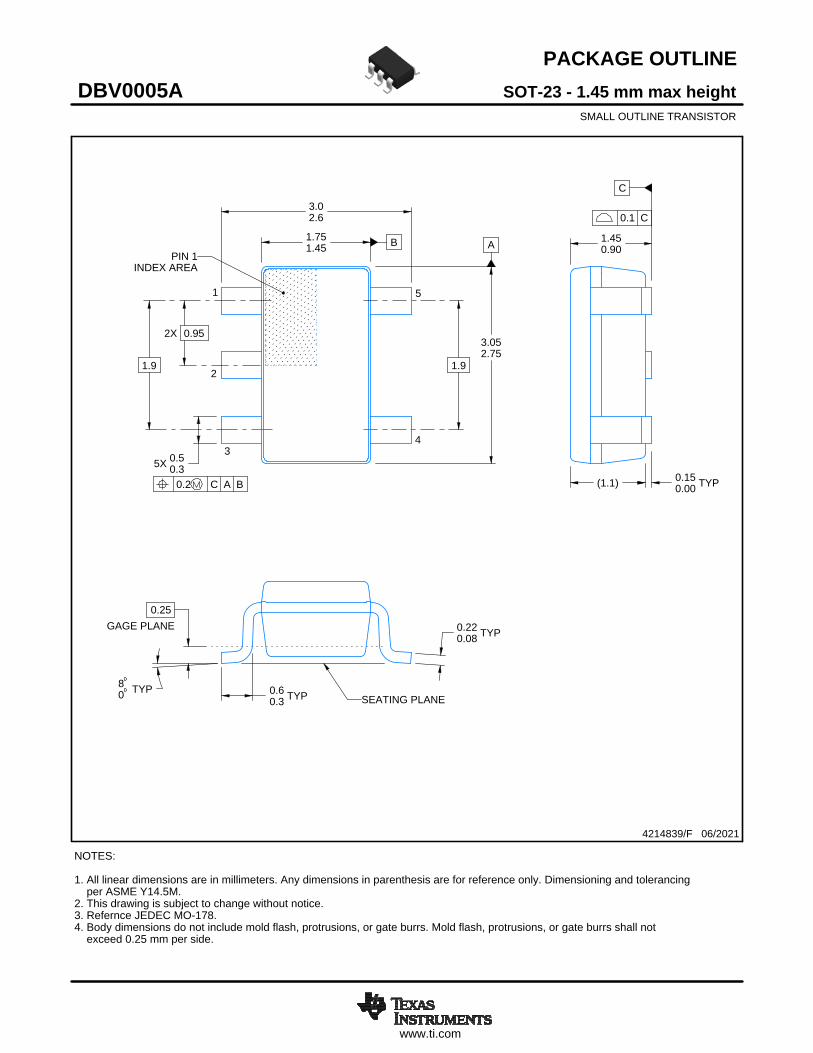
SOT-23 - 1.45 mm max heightDBV0005ASMALL OUTLINE TRANSISTOR
4214839/F 06/2021
NOTES: 1. All linear dimensions are in millimeters. Any dimensions in parenthesis are for reference only. Dimensioning and tolerancing per ASME Y14.5M.2. This drawing is subject to change without notice.3. Refernce JEDEC MO-178.4. Body dimensions do not include mold flash, protrusions, or gate burrs. Mold flash, protrusions, or gate burrs shall not exceed 0.25 mm per side.
0.2 C A B
1
34
5
2
INDEX AREAPIN 1
GAGE PLANE
SEATING PLANE
0.1 C
SCALE 4.000

www.ti.com
EXAMPLE BOARD LAYOUT
0.07 MAXARROUND
0.07 MINARROUND
5X (1.1)
5X (0.6)
(2.6)
(1.9)
2X (0.95)
(R0.05) TYP
4214839/F 06/2021
SOT-23 - 1.45 mm max heightDBV0005ASMALL OUTLINE TRANSISTOR
NOTES: (continued) 5. Publication IPC-7351 may have alternate designs. 6. Solder mask tolerances between and around signal pads can vary based on board fabrication site.
SYMM
LAND PATTERN EXAMPLEEXPOSED METAL SHOWN
SCALE:15X
PKG
1
3 4
5
2
SOLDER MASKOPENINGMETAL UNDER
SOLDER MASK
SOLDER MASKDEFINED
EXPOSED METAL
METALSOLDER MASKOPENING
NON SOLDER MASKDEFINED
(PREFERRED)
SOLDER MASK DETAILS
EXPOSED METAL

www.ti.com
EXAMPLE STENCIL DESIGN
(2.6)
(1.9)
2X(0.95)
5X (1.1)
5X (0.6)
(R0.05) TYP
SOT-23 - 1.45 mm max heightDBV0005ASMALL OUTLINE TRANSISTOR
4214839/F 06/2021
NOTES: (continued) 7. Laser cutting apertures with trapezoidal walls and rounded corners may offer better paste release. IPC-7525 may have alternate design recommendations. 8. Board assembly site may have different recommendations for stencil design.
SOLDER PASTE EXAMPLEBASED ON 0.125 mm THICK STENCIL
SCALE:15X
SYMM
PKG
1
3 4
5
2


IMPORTANT NOTICE AND DISCLAIMERTI PROVIDES TECHNICAL AND RELIABILITY DATA (INCLUDING DATASHEETS), DESIGN RESOURCES (INCLUDING REFERENCEDESIGNS), APPLICATION OR OTHER DESIGN ADVICE, WEB TOOLS, SAFETY INFORMATION, AND OTHER RESOURCES “AS IS”AND WITH ALL FAULTS, AND DISCLAIMS ALL WARRANTIES, EXPRESS AND IMPLIED, INCLUDING WITHOUT LIMITATION ANYIMPLIED WARRANTIES OF MERCHANTABILITY, FITNESS FOR A PARTICULAR PURPOSE OR NON-INFRINGEMENT OF THIRDPARTY INTELLECTUAL PROPERTY RIGHTS.These resources are intended for skilled developers designing with TI products. You are solely responsible for (1) selecting the appropriateTI products for your application, (2) designing, validating and testing your application, and (3) ensuring your application meets applicablestandards, and any other safety, security, or other requirements. These resources are subject to change without notice. TI grants youpermission to use these resources only for development of an application that uses the TI products described in the resource. Otherreproduction and display of these resources is prohibited. No license is granted to any other TI intellectual property right or to any third partyintellectual property right. TI disclaims responsibility for, and you will fully indemnify TI and its representatives against, any claims, damages,costs, losses, and liabilities arising out of your use of these resources.TI’s products are provided subject to TI’s Terms of Sale (https:www.ti.com/legal/termsofsale.html) or other applicable terms available eitheron ti.com or provided in conjunction with such TI products. TI’s provision of these resources does not expand or otherwise alter TI’sapplicable warranties or warranty disclaimers for TI products.IMPORTANT NOTICE
Mailing Address: Texas Instruments, Post Office Box 655303, Dallas, Texas 75265Copyright © 2021, Texas Instruments Incorporated