tpic74100-q1 buck/boost switch-mode regulator continuous and discontinuous conduction modes..... 4 3...
TRANSCRIPT

Application ReportSLIA083B–May 2007–Revised September 2010
TPIC74100-Q1 Buck/Boost Switch-Mode Regulator
Michael Weitz ................................................................................................. Mixed Signal Automotive
ABSTRACTThis document explains the features and benefits of the TPIC74100 buck/boost switch-mode regulator,which has been designed for automotive power-management applications.
It is meant as a guideline to achieve a good configuration of the device.
The configuration of the device is dependent on the individual application. Important topics required forthis evaluation are covered. The different operating modes of the device are explained. Help for theselection criteria of external components is given and example calculations are included. In addition, thereare rules and hints for an optimized layout and some information about evaluating the thermal conditionwithin the application.
Contents1 Introduction .................................................................................................................. 22 Description ................................................................................................................... 33 Selection of External Components ...................................................................................... 114 PCB Layout ................................................................................................................. 185 Thermal Analysis .......................................................................................................... 206 Summary ................................................................................................................... 227 References ................................................................................................................. 23
List of Figures
1 Schematic With Typical External Components ......................................................................... 22 Continuous and Discontinuous Conduction Modes .................................................................... 43 Equivalent Schematics – Buck Mode .................................................................................... 54 Ideal Buck Converter, Continuous Conduction, IL and VOUT vs Time ................................................. 55 Equivalent Schematics – Boost Mode.................................................................................... 66 Ideal Boost Converter, Continuous Conduction, IL and VOUT vs Time ................................................ 67 Mode Transition ............................................................................................................. 78 Primary and Secondary Output Voltage Terminals..................................................................... 89 SVS Circuit ................................................................................................................. 1510 PWP Package With Thermal Pad ....................................................................................... 1811 Thermal Vias With Multilayer Board (Side View)...................................................................... 18
List of Tables
1 Modulator Frequency ..................................................................................................... 142 Slew Rate Selection....................................................................................................... 143 Component Placement Priority List ..................................................................................... 19
PowerPAD is a trademark of Texas Instruments.
1SLIA083B–May 2007–Revised September 2010 TPIC74100-Q1 Buck/Boost Switch-Mode RegulatorSubmit Documentation Feedback
Copyright © 2007–2010, Texas Instruments Incorporated
Switch Mode
Controller with
Dead Time
Charge
Pump
Vref
BandgapRef
Vreg Osc
+
-
+
-
POR With
Delay Timer
Vdriver
ENABLE
GND
L1
5 V Supply
5Vg_Supply
-
+
L2
VOUT
Q1
Q2
Q3
Q4
RESET
Temp
Monitor
Shutdown
Regulator
Rmod ClockModulator
Cboot1
Cboot2
5Vg_ENABLE
AOUT
REST
PGND
SCR0
SCR1
Slew Rate
Control
5Vg
Low Power
Mode
Control
CLP
In-Rush
Current Limit
4.7 nF
4.7 nF
5 kΩ
5 kΩ
12 kΩ
R1
R2
L
C
470 nF
2.2 nF - 150 nF
ChargePump
BandgapRef
Vlogic
AIN
Vbattery
33 µH
47 µF - 470 µF
1 µF - 100 µF
Ignition
Low Power ModeDigital Signal
Introduction www.ti.com
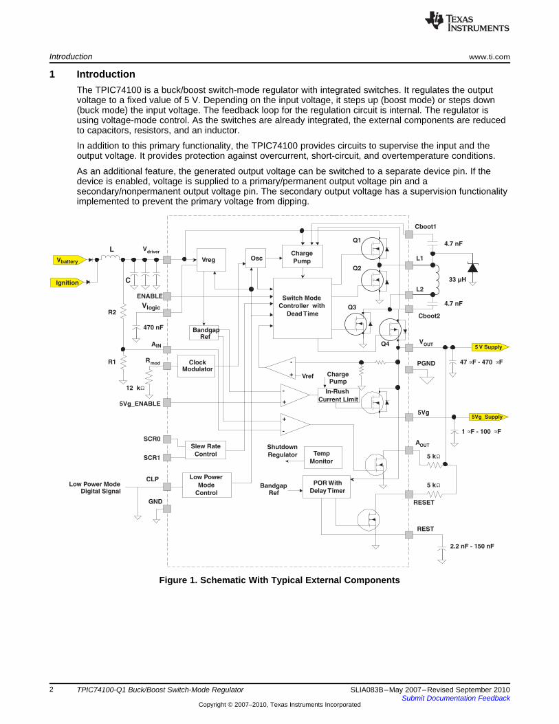
1 IntroductionThe TPIC74100 is a buck/boost switch-mode regulator with integrated switches. It regulates the outputvoltage to a fixed value of 5 V. Depending on the input voltage, it steps up (boost mode) or steps down(buck mode) the input voltage. The feedback loop for the regulation circuit is internal. The regulator isusing voltage-mode control. As the switches are already integrated, the external components are reducedto capacitors, resistors, and an inductor.
In addition to this primary functionality, the TPIC74100 provides circuits to supervise the input and theoutput voltage. It provides protection against overcurrent, short-circuit, and overtemperature conditions.
As an additional feature, the generated output voltage can be switched to a separate device pin. If thedevice is enabled, voltage is supplied to a primary/permanent output voltage pin and asecondary/nonpermanent output voltage pin. The secondary output voltage has a supervision functionalityimplemented to prevent the primary voltage from dipping.
Figure 1. Schematic With Typical External Components
2 TPIC74100-Q1 Buck/Boost Switch-Mode Regulator SLIA083B–May 2007–Revised September 2010Submit Documentation Feedback
Copyright © 2007–2010, Texas Instruments Incorporated

www.ti.com Description
2 Description
2.1 Features and Benefits• Switch-Mode Regulator With Integrated Switches
– Less board space– Lower cost– Higher EMI performance– Improved protection off the integrated switches
• Buck/Boost Mode– Wide input voltage range (ideal for automotive applications where the power supply must stay
stable during the start of the engine-cranking pulse)• Low-Power Operation Mode
– Conserves battery power during conditions with low load current• Second Output Voltage With Enable Function
– The primary/permanent output voltage can be switched to a second pin, which acts as a secondoutput voltage with enable function.
– Soft-start for second output voltage implemented– Conserve battery power by disabling second output voltage under certain conditions– VOUT voltage is protected from failures of the 5Vg line
• Device Enable Function– Conserve battery power during system shutdown by disabling the device
• Enhanced EMI Performance– Programmable frequency modulation – spread spectrum– Programmable slew rate
• Supervision Functionality– Supervision of input voltage, programmable under-voltage detection threshold, and open-drain
output for generation of alarm signal– Supervision of output voltage, programmable delay timer, and open-drain output for generation of
reset signal, e.g., for supervisor microcontroller• Current Limit
– Protection in case of overcurrent and short-circuit conditions• Thermal Shutdown
– Protection in case of overtemperature conditions
3SLIA083B–May 2007–Revised September 2010 TPIC74100-Q1 Buck/Boost Switch-Mode RegulatorSubmit Documentation Feedback
Copyright © 2007–2010, Texas Instruments Incorporated
Continuous conduction mode
Discontinuous conduction mode
IL
ILaverage
IL
ILaverage
tON tOFF
tON tOFF tIDLE
Description www.ti.com
2.2 Operating Modes
2.2.1 Start-UpIt is important to consider the separate specification for the input voltage Vdriver during start-up of the device(setting ENABLE pin from low to high). The device is not able to start up with the lowest specified inputvoltage.
During start-up, the device internal power supply Vlogic is fed by the input voltage at Vdriver. After start-up, itis fed by the output voltage and is no longer dependent of the input voltage (see the TPIC74100 datasheet in the Electrical Characteristics section, parameter Vdriver Start-up condition voltage).
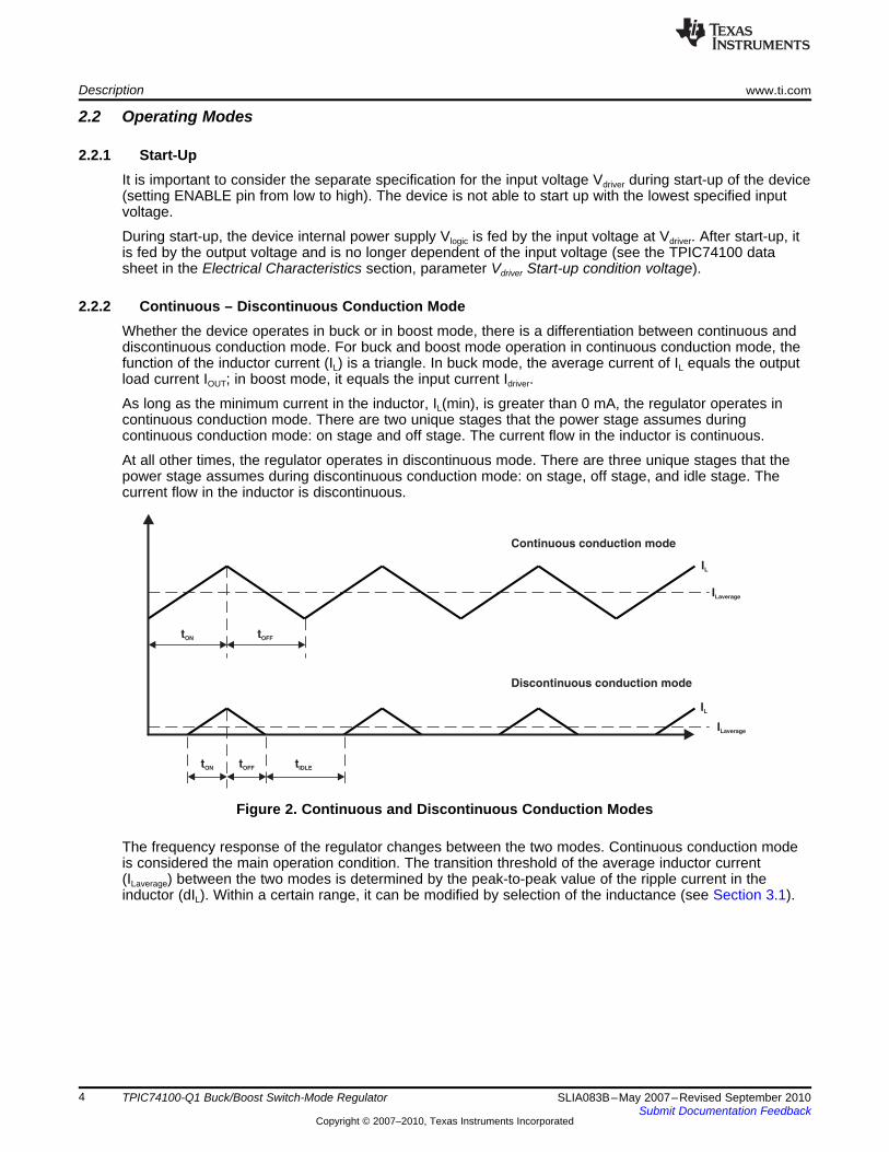
2.2.2 Continuous – Discontinuous Conduction ModeWhether the device operates in buck or in boost mode, there is a differentiation between continuous anddiscontinuous conduction mode. For buck and boost mode operation in continuous conduction mode, thefunction of the inductor current (IL) is a triangle. In buck mode, the average current of IL equals the outputload current IOUT; in boost mode, it equals the input current Idriver.
As long as the minimum current in the inductor, IL(min), is greater than 0 mA, the regulator operates incontinuous conduction mode. There are two unique stages that the power stage assumes duringcontinuous conduction mode: on stage and off stage. The current flow in the inductor is continuous.
At all other times, the regulator operates in discontinuous mode. There are three unique stages that thepower stage assumes during discontinuous conduction mode: on stage, off stage, and idle stage. Thecurrent flow in the inductor is discontinuous.
Figure 2. Continuous and Discontinuous Conduction Modes
The frequency response of the regulator changes between the two modes. Continuous conduction modeis considered the main operation condition. The transition threshold of the average inductor current(ILaverage) between the two modes is determined by the peak-to-peak value of the ripple current in theinductor (dIL). Within a certain range, it can be modified by selection of the inductance (see Section 3.1).
4 TPIC74100-Q1 Buck/Boost Switch-Mode Regulator SLIA083B–May 2007–Revised September 2010Submit Documentation Feedback
Copyright © 2007–2010, Texas Instruments Incorporated

T = t + tP ON OFFI = ILaverage OUT
VOUT
VIN
tON
TP
= D=
DischargeCOUT
ChargeCOUT
tOFFtON
IL
ILaverage
VOUT
L
COUT
Rload
VOUT
VIN
Buck Mode: tON
Buck Mode: tOFF
ESR
L
COUT
Rload
VOUT
VIN
ESR
www.ti.com Description
2.2.3 Buck ModeIn buck mode, the device is stepping/converting down the input voltage, so Vdriver > VOUT.
Figure 3 shows the equivalent schematic for the on and off phases while operating in continuousconduction buck mode. The on and off phases relate to the status of the high-side switch, Q1, which isconnected to the input voltage VIN = Vdriver.
Figure 3. Equivalent Schematics – Buck Mode
During the on phase, the current in the inductor is increasing; during the off phase, it is decreasing. Theaverage current in the Inductor is equal to the output load current (IOUT). As long as the inductor current ishigher than the output load current, the output capacitor (COUT) is charging. If it is lower than the outputload current, COUT is discharging.
Figure 4. Ideal Buck Converter, Continuous Conduction, IL and VOUT vs Time
5SLIA083B–May 2007–Revised September 2010 TPIC74100-Q1 Buck/Boost Switch-Mode RegulatorSubmit Documentation Feedback
Copyright © 2007–2010, Texas Instruments Incorporated
T = t + tP ON OFFI = ILaverage IN
VOUT
VIN
TP
T – tP ON
= =1
1 – D
ChargeCOUT
DischargeCOUT
tOFFtON
IL
IINaverage
VOUT
L
Rload
VOUT
VIN
Boost Mode: tON
L
VIN
Boost Mode: tOFF
COUT
ESR
Rload
VOUT
COUT
ESR
Description www.ti.com
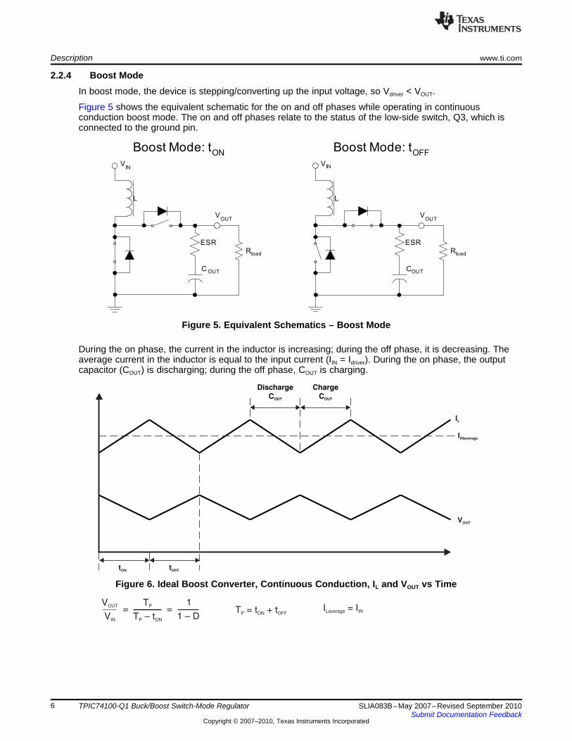
2.2.4 Boost ModeIn boost mode, the device is stepping/converting up the input voltage, so Vdriver < VOUT.
Figure 5 shows the equivalent schematic for the on and off phases while operating in continuousconduction boost mode. The on and off phases relate to the status of the low-side switch, Q3, which isconnected to the ground pin.
Figure 5. Equivalent Schematics – Boost Mode
During the on phase, the current in the inductor is increasing; during the off phase, it is decreasing. Theaverage current in the inductor is equal to the input current (IIN = Idriver). During the on phase, the outputcapacitor (COUT) is discharging; during the off phase, COUT is charging.
Figure 6. Ideal Boost Converter, Continuous Conduction, IL and VOUT vs Time
6 TPIC74100-Q1 Buck/Boost Switch-Mode Regulator SLIA083B–May 2007–Revised September 2010Submit Documentation Feedback
Copyright © 2007–2010, Texas Instruments Incorporated

Device Startup
V < ~5.8 Vdriver
No
Yes
Boost Mode
V > ~5.8 Vdriver
No
Yes
Buck Mode
V < ~5.8 V
andV ~ 4.9 V
driver
OUTNo
Yes
www.ti.com Description
2.2.5 Transition Buck / Boost ModeThe transition between buck and boost mode isdone automatically and has almost no impacton the output voltage (VOUT).
These points must be considered:• Output voltage tolerance increases to worst
case value of ±3% instead of ±2% during thetransition between the two modes.
• Output current capability decreases withdecreasing input voltage (Vdriver) in boostmode.
The increased output voltage tolerance isspecified for the transition phase from buck toboost and from boost to buck.• Transition from boost to buck occurs during
increasing Vdriver voltage at the threshold of5.8 V (typical).
• Transition from buck to boost occurs duringdecreasing Vdriver voltage, within the so-called crossover window, from 5.8 V (typical)down to 5 V (typical).
The exact threshold for the transition betweenthe modes is dependent on the input voltageVdriver, the load current IOUT, and the externalcomponents.
The increased tolerance during the transition isprimarily required for conditions with low loadcurrents. Ripple of the output voltage in generalimproves for higher load current conditions.
Figure 7. Mode Transition
2.2.6 Low-Power ModeTo increase the efficiency at low output load currents, the device can be switched into a low-poweroperation mode. Output load currents are considered low if the device operates in discontinuousconduction mode.
During normal operation with no low-power mode activated, the device is works in pulse-width modulation(PWM) mode. The switching frequency remains constant, and regulation is accomplished by variation ofthe duty cycle. In low-power mode, the device is working in pulse-frequency modulation (PFM) mode.Regulation is accomplished by variation of the switching frequency.
There is no reduced load current capability for the output load in PFM mode. Efficiency is lower and outputvoltage ripple is larger than in PWM mode for higher load currents. Low-power mode functionality isimplemented for buck-mode operation. In boost-mode conditions, the device automatically operates inPWM mode. When low-power mode is enabled, the transition between buck and boost is also a transitionbetween PWM mode and PFM mode.
2.2.7 Secondary Output VoltageThe secondary output voltage (5Vg) can be switched on and off while the device is enabled. Internally, theprimary output voltage VOUT is shared to the 5Vg pin.
7SLIA083B–May 2007–Revised September 2010 TPIC74100-Q1 Buck/Boost Switch-Mode RegulatorSubmit Documentation Feedback
Copyright © 2007–2010, Texas Instruments Incorporated
VOUT
47 µF
5Vg
100 µF
5VG_ENABLERESET
Vdriver
47 µF
Q1
Q2
33 µH
Q4Q3
L1 L2SwitchControl
Buck/BoostGate Driver
Peak Current Limit
Slew Rate Control
VOUT
Typ ~ V – 100 mVOUT
V
Typ 4.65 VOUT
5Vg
RESET
Charge Pump
RESET Deglitch
GateDriver
Description www.ti.com
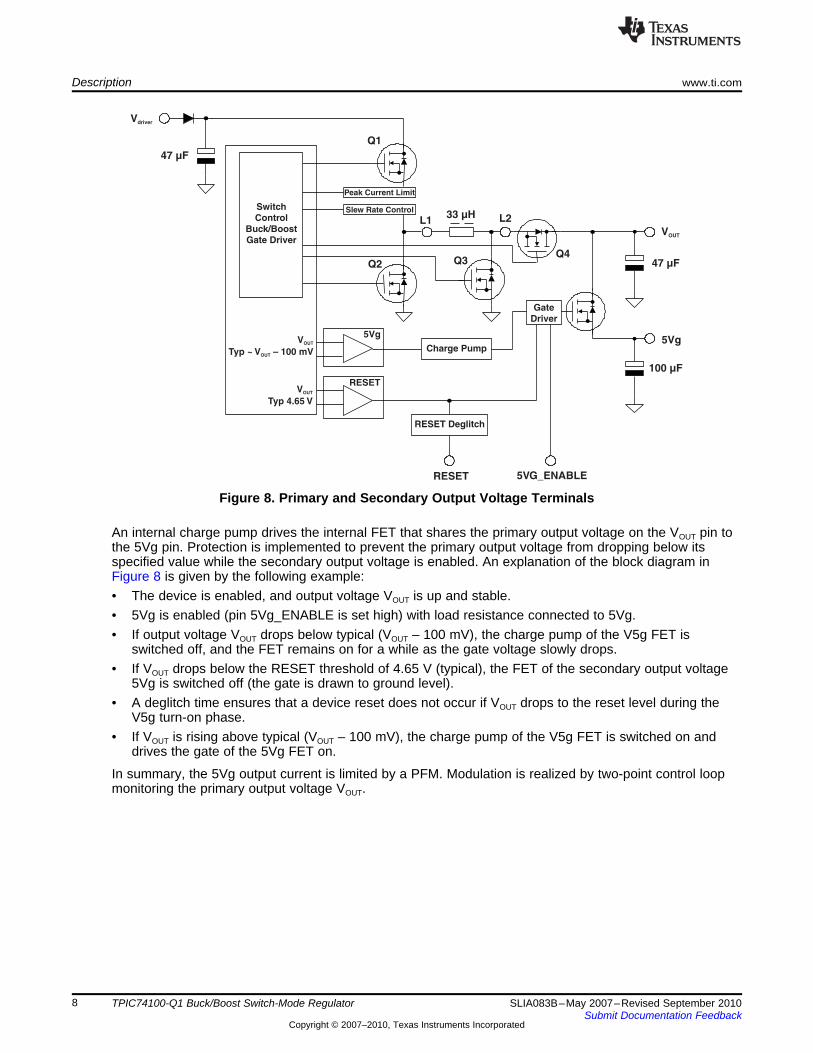
Figure 8. Primary and Secondary Output Voltage Terminals
An internal charge pump drives the internal FET that shares the primary output voltage on the VOUT pin tothe 5Vg pin. Protection is implemented to prevent the primary output voltage from dropping below itsspecified value while the secondary output voltage is enabled. An explanation of the block diagram inFigure 8 is given by the following example:• The device is enabled, and output voltage VOUT is up and stable.• 5Vg is enabled (pin 5Vg_ENABLE is set high) with load resistance connected to 5Vg.• If output voltage VOUT drops below typical (VOUT – 100 mV), the charge pump of the V5g FET is
switched off, and the FET remains on for a while as the gate voltage slowly drops.• If VOUT drops below the RESET threshold of 4.65 V (typical), the FET of the secondary output voltage
5Vg is switched off (the gate is drawn to ground level).• A deglitch time ensures that a device reset does not occur if VOUT drops to the reset level during the
V5g turn-on phase.• If VOUT is rising above typical (VOUT – 100 mV), the charge pump of the V5g FET is switched on and
drives the gate of the 5Vg FET on.
In summary, the 5Vg output current is limited by a PFM. Modulation is realized by two-point control loopmonitoring the primary output voltage VOUT.
8 TPIC74100-Q1 Buck/Boost Switch-Mode Regulator SLIA083B–May 2007–Revised September 2010Submit Documentation Feedback
Copyright © 2007–2010, Texas Instruments Incorporated

www.ti.com Description
2.2.8 Other Operating Conditions/ModesOvervoltage Protection Circuit for VOUT
The overvoltage protection circuit for VOUT prevents the output voltage from rising above the specifiedboundaries. It activates during operation in discontinuous conduction mode at very low load currents.
In discontinuous mode, the minimum on time tON determines the minimum amount of energy that ispumped into the inductance. Once in the inductance, the energy is transferred to the output terminal, VOUT.In other words, every triangle of the inductor current in discontinuous conduction mode (see Figure 2)transfers a minimum amount of energy to the output. If the output load current consumes less than thisamount, the output voltage would rise without the protection circuit.
The overvoltage protection circuit monitors the output voltage and skips the ON phase (that is, it does notswitch on the high-side FET Q1) if VOUT is higher than 5.08 V (typical). By skipping the ON phase, a PFMmode is realized within the operation in PWM mode.
Synchronous/Nonsynchronous ModeTo prevent the current in the inductance from reverting during the OFF phase at low load currents(discontinuous conduction mode) in buck mode, the low-side FET Q2 is not switched on. Current flowduring OFF phase is through the free-wheeling diode of the low-side FET Q2 and the external Schottkydiode. A reverting current in the inductance would add losses and decrease efficiency. When this occurs,the regulator is working in nonsynchronous mode.
If the peak current measured in the high-side FET Q1 exceeds 450 mA (typical), the low-side FET Q2 isswitched ON during the OFF phase (see Figure 3). Voltage drop across the diode is now reduced to thevoltage drop across the ON resistance of the low-side FET Q2 (RDS ON). In this case, the regulator isworking in synchronous mode with an increased efficiency.
Slew Rate ControlThe slew rate settings control the input current rate of the high-side FET Q1 in buck mode. Buck mode isthe most critical mode, because of the high ripple currents at the input terminal Vdriver. The slew rate controlgives the option to improve EMI performance by selecting slower slew rate settings or to improveefficiency by selecting faster slew rate settings (see typical oscilloscope plots of different slew rate settingin the data sheet).
Peak Current LimitIn buck mode, the peak current limit circuit monitors the current flow through the high-side FET Q1, whichis connected to the Vdriver terminal. If a current higher than the peak current limit threshold of 2 A (typical) isdetected, FET Q1 is switched off. There is a turn-off delay for the FET of 100 ns (typical). FET Q1 can beturned on again in the next cycle of the switching period. In low-power mode, the peak current limit isreduced to 1 A (typical).
In boost mode, the gate of the high-side FET Q1 is pulled down if the peak current limit threshold of2 A (typical) is detected. The average current limit is dependent of the external configuration (e.g.,capacitor size at VOUT, RDS ON of the inductor, etc.). It is slightly higher in boost mode than in buck mode.
The slope of the inductor current determines the actual peak current. The slope of the inductor current canbecome very large if the inductor is operated in saturation. If the peak current limit is meant as short-circuitprotection for the application, an inductor with appropriate saturation current (ISAT) must be selected.Otherwise, the inductor could be destroyed under a short-circuit condition (see Section 3.1).
9SLIA083B–May 2007–Revised September 2010 TPIC74100-Q1 Buck/Boost Switch-Mode RegulatorSubmit Documentation Feedback
Copyright © 2007–2010, Texas Instruments Incorporated

Description www.ti.com
2.3 EMI performance
2.3.1 Modulation of the Switching FrequencyModulation of the switching frequency can improve the EMI performance by spreading the emittedspectrum of the switch-mode regulator (frequency spread-spectrum method).
The switching frequency of the regulator can be modulated with the clock modulator frequency. Thismodulation frequency can be selected with an external resistor from the Rmod pin to the GND pin.
By modulating the switching frequency, its spectral line sweeps back and forth accordingly in thefrequency spectrum. The nonmodulated spectral line of the switching frequency is transformed into aspectral band by modulation, causing emitted peak values to decrease. The speed of the sweep isadjusted with the modulator frequency, while the span of the sweep remains constant.
It is not possible to switch on the modulation if the device is already enabled. The check for an externalresistor connected to Rmod is only performed once when the device is enabled.
2.3.2 Selection of the Slew RateThe slew rate of the regulator can be programmed in four stages. Depending on application requirements,device operation can be optimized for EMI performance or for high efficiency. Faster slew rates result inhigher efficiency, and slower slew rates result in better EMI performance.
2.3.3 Adjustment of the Ripple CurrentAnother way to improve the EMI performance is to reduce the ripple current in the inductor. The ripplecurrent can be adjusted by the selection of external components.
2.3.4 External Schottky DiodeThe external Schottky diode optimizes the regulator for EMI performance and efficiency. It is required forstable operation and placed between pins L1 and PGND.
In buck mode, the voltage drop at the low-side FET Q2 during the off period is determined by its onresistance (rDS(on)). The voltage drop is limited by the forward voltage of the internal diode of the FET Q2(free-wheeling diode). There is a dead time when both switches are OFF during the transition from ON toOFF. During the dead time, the voltage drop is defined by the forward voltage of the internal diode or theexternal Schottky diode. With the lower forward voltage of a Schottky diode, the voltage drop is reduced.
For high-power applications, a lower voltage drop means increased efficiency. The fast response time ofthe Schottky diode also has a positive effect on EMI performance. In addition, part of the overall thermaldissipation loss is transferred from the TPIC74100 to the external Schottky diode.
10 TPIC74100-Q1 Buck/Boost Switch-Mode Regulator SLIA083B–May 2007–Revised September 2010Submit Documentation Feedback
Copyright © 2007–2010, Texas Instruments Incorporated

Buck Mode:
Boost Mode:
IL_average IOUT
IRMS_OUT
0.29 VOUT 1 VOUT
V IN
L fSW
0.29 dIL
IRMS_L IRMS_OUT
IL_average IIN
IRMS_driver 13 dIL
(VOUT VIN) V IN
3 L fSW VOUT
IRMS_L IRMS_driver
Buck Mode:
Boost Mode:
L(V IN VOUT) VOUT
fSW dIL V INdIL
(VIN VOUT) VOUT
fSW L V IN
L(VOUT V IN) V IN
fSW dIL VOUT
dIL(VOUT VIN) VIN
fSW L VOUT
www.ti.com Selection of External Components
3 Selection of External Components
3.1 InductorInductance• Recommended inductance range: 22 μH to 100 μH• Define the tolerable ripple current (e.g., dIL = 0.2 × IOUT) and calculate the inductance.• Another option is to calculate the ripple current at a given inductance.• The size of the ripple current (dIL) determines the threshold for the regulator to operate in continuous or
discontinuous conduction mode, which might impact EMI behavior (see Section 2.2.2).• A larger inductance value results in lower current ripple, better EMI performance, but it also results in
slower response to fast load transients, due to the larger amount of stored energy in the inductor.
DC Resistance (DCR)• Low DCR is required to reduce losses and achieve high efficiency.
Saturation Current (ISAT)• For a short-circuit proof design, the saturation current (ISAT) of the inductor should be equal to or
greater than the internal peak current limit.
Root Mean Square (RMS) Current (IRMS)• The RMS current in the inductor causes the temperature of the inductor to rise a specific amount
above ambient temperature.
3.2 Input CapacitorAn external filter capacitor is required at the input terminal Vdriver. The capacitor needs to support peakcurrents to reduce voltage ripple at Vdriver and minimize noise. For the input capacitor, buck mode causesmuch more stress than boost mode. The following key parameters need to be considered for the selectionof CIN.
Capacitance• For most applications, the requirements for high RMS current rating and low ESR determine the
minimum available capacitance.• Recommended capacitance is 22 μF to 470 μF.
Equivalent Series Resistance (ESR)• Low ESR required to reduce voltage ripple at the input Vdriver.• A low-ESR aluminum or tantalum-type capacitor with ESR < 200 mΩ is recommended.
11SLIA083B–May 2007–Revised September 2010 TPIC74100-Q1 Buck/Boost Switch-Mode RegulatorSubmit Documentation Feedback
Copyright © 2007–2010, Texas Instruments Incorporated

Buck Mode:
Boost Mode:
dVOUT dVESR_COUNT dVCOUT dIL ESRCOUT 1
8 COUT fSW
dVCOUT IOUT D
COUT fSW
IOUT 1 V IN
VOUT
COUT fSW
dVOUT dVESR_COUNT dVCOUT
dVESR_COUT_MAX IOUT
1 D
dIL
2 ESRCOUT IOUT VOUT
V IN
dIL
2 ESRCOUNT
Buck Mode:
Boost Mode:
IRMS_driver IOUT D D2 IOUT VOUT (VIN VOUT)
(V IN)2
Worst Case: D 50%.V IN 2 VOUT : IRMS_driver IOUT
2
IRMS_driver 13 dIL
(VOUT VIN) V IN
3 L fSW VOUT
Worst Case: D 50%.VOUT 2 V IN : IRMS_driver VOUT
12 L fSW
Selection of External Components www.ti.com
Voltage Rating• Approximately 1.5 times the maximum applied voltage at Vdriver for an aluminum-type capacitor• Approximately two times the maximum applied voltage at Vdriver for a tantalum-type capacitor
Equivalent Series Inductance (ESL)• Choose low ESL capacitors to avoid potential problems with ringing in the lower MHz range.
RMS Current Rating• RMS value of the input ripple current (IRMS_driver) heats up input capacitor CIN due to it is internal ESR.
This rating is especially critical in buck mode.
In parallel to the filter capacitor at the input terminal on Vdriver, a fast ceramic-type capacitor isrecommended for EMI performance reasons.
3.3 Output CapacitorsAn external filter capacitor is required at the output pins VOUT and 5Vg. The capacitors must support thepeak currents to reduce voltage ripple at VOUT and minimize noise. For the output capacitor, boost modecauses much more stress than buck mode. Filtering of the output voltage is done by COUT at the VOUT pin.The on resistance of the 5Vg FET (rDS(on)) limits the filter capability of C5Vg. The following key parametersmust be considered for the selection of COUT and C5Vg.
Capacitance• Capacitance influences the output voltage ripple, but the ESR of the capacitor has more influence (see
the following formulas).• Recommended capacitance COUT is 22 μF to 470 μF.• Recommended capacitance C5Vg is 1 μF to 100 μF.• Total capacitance (COUT + C5Vg) must be equal or less than 470 μF.
Equivalent Series Resistance (ESR)• Low ESR is required to reduce voltage ripple at VOUT.• A low ESR aluminum or tantalum type capacitor is recommended.• Ripple of the output voltage is mainly determined by the ESR value.
12 TPIC74100-Q1 Buck/Boost Switch-Mode Regulator SLIA083B–May 2007–Revised September 2010Submit Documentation Feedback
Copyright © 2007–2010, Texas Instruments Incorporated

Buck Mode:
Boost Mode:
IRMS_OUT
0.29 VOUT 1 VOUT
V IN
L fSW
0.29 dIL
IRMS_OUT IOUT VOUT VIN
VIN
IOUT D
1 D
www.ti.com Selection of External Components
Voltage Rating• Approximately 1.5 times the output voltage at VOUT for an aluminum type capacitor• Approximately two times the output voltage at VOUT for a tantalum type capacitor
Equivalent Series Inductance (ESL)• Choose low ESL capacitors to avoid potential problems with ringing in the lower MHz range.
RMS Current Rating• RMS value of the output ripple current IRMS_OUT heats up the output capacitor (COUT) due to its internal
ESR. This rating is especially critical in boost mode.
3.4 Stability ConsiderationsThe TPIC74100 is a voltage-mode controlled regulator with fully integrated feedback loop, error amplifier,and compensation. No further external components are required.
The main external influence to the frequency and phase response of the TPIC74100 is determined by theoutput filter. Inductor and output capacitor should be selected within the following range:
Inductor L (inductance): Min: 22 μH Max: 100 μHCapacitor COUT (capacitance): Min: 22 μF Max: 470 μF (COUT + C5Vg)
Series resistance of the output capacitor:
ESRC 22 μH ≥ L ≤ 68 μH22 μF ≥ COUT ≤ 470 μF: Min: 50 mΩ Max: 500 mΩ
68 μH > L ≤ 100 μH22 μF ≥ COUT < 33μF: Min: 100 mΩ Max: 500 mΩ33 μF ≥ COUT ≤ 470μF: Min: 50 mΩ Max: 500 mΩ
The following values are recommended by TI for best performance:• L = 33 μH• C = 47 μF• ESRC = 50 mΩ to 100 mΩ
13SLIA083B–May 2007–Revised September 2010 TPIC74100-Q1 Buck/Boost Switch-Mode RegulatorSubmit Documentation Feedback
Copyright © 2007–2010, Texas Instruments Incorporated

Selection of External Components www.ti.com
3.5 External Schottky DiodeDC Blocking Voltage/Reverse Voltage (VR)• VR ≥ maximum input voltage at Vdriver terminal• Recommendation: VR ≥ 40 V
Feed Forward Voltage• Maximum voltage drop at 125°C < 0.4 V
Average Rectified Forward Current (IO)• IO ≥ maximum specified load current IOUT
• For a short-circuit proof design, IO must be greater than the internal peak current limit.
See Section 2.3.4.
3.6 Modulator FrequencySelection is done via external resistor at pin Rmod to GND. The resistor is checked only once when thedevice is enabled. If no resistor is detected, the functionality is disabled. This means the modulationcannot be enabled while the device is operating.
Table 1. Modulator FrequencyMinimum Switching Frequency Maximum Modulation FrequencyRmod f(mod) f(SW_MIN) f(SW_MAX)
0 kΩ 0 kHz f(SW_MIN) = f(SW) f(SW_MAX) = f(SW)
12 kΩ 28 kHz (typ) f(SW_MIN) = f(SW) – modulation span f(SW_MAX) = f(SW) + modulation span24 kΩ 56 kHz (typ) f(SW_MIN) = f(SW) – modulation span f(SW_MAX) = f(SW) + modulation span
The external resistor determines the period T(mod) it takes for the switching frequency f(SW) to sweep fromthe modulation minimum frequency to the modulation maximum frequency. Modulation minimum andmaximum frequency and resulting modulation span (maximum modulation frequency – minimummodulation frequency) are not dependent on the modulation frequency.
Modulation of the switching frequency increases EMI performance (see Section 2.3.1).
3.7 Slew Rate SelectionThe pins SCR0 and SCR1 do not support full input voltage range of Vdriver (see the maximum ratingsspecified in the data sheet). Usually they are connected to Vlogic or VOUT.
Table 2. Slew Rate Selection
SCR1 SCR0 SRQ1 EMI Performance EfficiencyGND GND Slowest slew rate Best case Worst caseGND HIGH Slow slew rateHIGH GND Fast slew rateHIGH HIGH Fastest slew rate Worst case Best case
14 TPIC74100-Q1 Buck/Boost Switch-Mode Regulator SLIA083B–May 2007–Revised September 2010Submit Documentation Feedback
Copyright © 2007–2010, Texas Instruments Incorporated
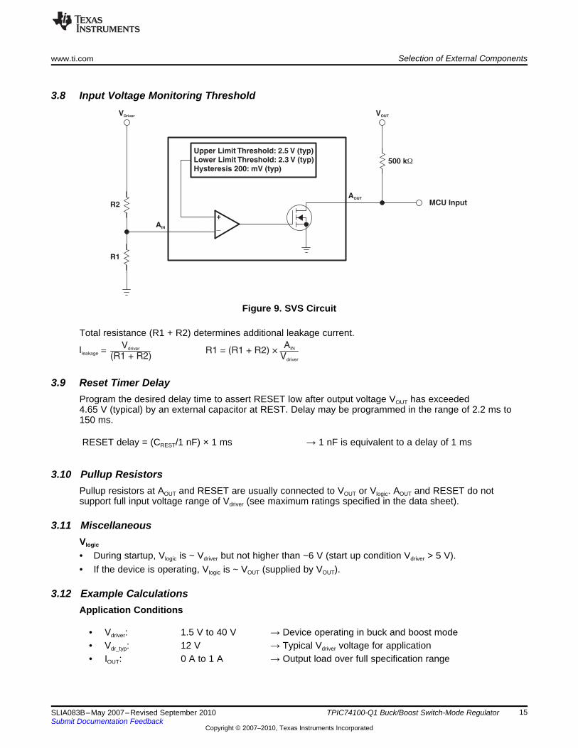
R1 = (R1 + R2) ×AIN
Vdriver
Vdriver
(R1 + R2)I =leakage
VOUT
MCU InputAOUT
R2
R1
VDriver
Upper Limit Threshold: 2.5 V (typ)Lower Limit Threshold: 2.3 V (typ)Hysteresis 200: mV (typ)
AIN
500 kW
www.ti.com Selection of External Components
3.8 Input Voltage Monitoring Threshold
Figure 9. SVS Circuit
Total resistance (R1 + R2) determines additional leakage current.
3.9 Reset Timer DelayProgram the desired delay time to assert RESET low after output voltage VOUT has exceeded4.65 V (typical) by an external capacitor at REST. Delay may be programmed in the range of 2.2 ms to150 ms.
RESET delay = (CREST/1 nF) × 1 ms → 1 nF is equivalent to a delay of 1 ms
3.10 Pullup ResistorsPullup resistors at AOUT and RESET are usually connected to VOUT or Vlogic. AOUT and RESET do notsupport full input voltage range of Vdriver (see maximum ratings specified in the data sheet).
3.11 MiscellaneousVlogic
• During startup, Vlogic is ~ Vdriver but not higher than ~6 V (start up condition Vdriver > 5 V).• If the device is operating, Vlogic is ~ VOUT (supplied by VOUT).
3.12 Example CalculationsApplication Conditions
• Vdriver: 1.5 V to 40 V → Device operating in buck and boost mode• Vdr_typ: 12 V → Typical Vdriver voltage for application• IOUT: 0 A to 1 A → Output load over full specification range
15SLIA083B–May 2007–Revised September 2010 TPIC74100-Q1 Buck/Boost Switch-Mode RegulatorSubmit Documentation Feedback
Copyright © 2007–2010, Texas Instruments Incorporated
dIL
2= I +IN
100 mA
2= 2 × 0.5 A + = 1.05 AI = I +L_peak L
dIL
2
VOUT
2= 2.5 V, I = 2 × I , I = ~500 mAIN OUT OUT_maxV =IN
I +L
dIL
2= I +OUT
350 mA
2= 1 A + = 1.18 AI =L_peak
dIL
2
dI =L= = 100 mA
(V – V ) × VOUT IN IN
f × L × VSW OUT
5 V
4 × 380 kHz × 33 µH=
VOUT
4 × f × LSW
dI =L= = 350 mA
(V – V ) × VIN OUT OUT
f × L × VSW IN
(40 V – 5 V) × 5 V
380 kHz × 33 µH × 40 V
L = = = 38 µH(V – V ) × VIN OUT OUT
f × dI × VSW L IN
(12 V – 5 V) × 5 V
380 kHz × 200 mA × 12 V
Selection of External Components www.ti.com
Inductor L
• Maximum ripple current: dI = 0.2 × IOUT = 0.2 × 1 A = 200 mA
• L for typical input driver voltage Vdriver = Vdr_typ = 12 V
Buck mode:
→ Selection: L = 33 μH• Check worst-case ripple current over operating conditions
Buck mode, worst case: VIN = Vdriver_max = 40 V
Boost mode, worst case: VIN = VOUT/2
→ Worst case: buck mode, dIL ≈ 350 mA• RMS current IRMS:
Buck mode, worst case: IRMS_OUT = 0.29 × dIL = 0.29 × 350 mA = 102 mABoost mode, worst case: IRMS_driver = ⅓ × dIL = ⅓ × 100 mA = 33 mA→ Worst case: buck mode, IRMS ≉≉ 100 mA
• Saturation current ISAT:
Buck mode, worst case:
Boost mode, worst case:(includes margin, specified is 200 mA for Vdriver = 2 V)
→ ISAT ≉≉ 1.2 A, considering short-circuit protection some added margin
Input Capacitor CIN
• RMS current rating IRMS
Buck mode, worst case: VIN = 2 × VOUT, IRMS_driver = IOUT/2 = 1 A/2 = 0.5 ABoost mode, worst case: IRMS_driver = ⅓ × dIL = ⅓ × 100 mA = 33 mA→ Worst case: buck mode, IRMS > 0.5 A
16 TPIC74100-Q1 Buck/Boost Switch-Mode Regulator SLIA083B–May 2007–Revised September 2010Submit Documentation Feedback
Copyright © 2007–2010, Texas Instruments Incorporated

ESRCOUT dVESR_COUT_MAX
IOUTVOUT
V IN
dIL
2 200 mV
350 mA 5 V1.5 V
100 mA2
164 m
COUT
IOUT 1 VIN
VOUT
dVCOUT fSW
350 mA 1 1.5 V
5 V
100 mV 380 kHz 6.4 F
_ 200
350570
ESR COUT
COUT
L
dV mVESR
dI mAm= = = W
COUT dIL1
8 dVCOUT fSW
350 mA 18 200 mV 380 kHz
576 nF
IRMS_out IOUT VOUT VIN
VIN
350 mA 5 V 1.5 V1.5 V
535 mA
www.ti.com Selection of External Components
Output Capacitor COUT
• RMS current rating IRMS
Buck mode, worst case: IRMS_OUT = 0.29 × dIL = 0.29 × 350 mA = 102 mABoost mode, worst case: VIN = Vdriver_min = 1.5 V
IOUT_max ≉ 350 mA (specified 200 mA, additional margin)
→ Worst case, boost mode, IRMS > 0.5 A• Output voltage ripple: → defined dVOUT ≤ 200 mV
Buck mode, minimum capacitance COUT:
Buck mode, maximum ESR for COUT:
Boost mode, minimum capacitance COUT:VIN = Vdriver_min = 1.5 V, IOUT_max ≉ 350 mA(specified 200mA, additional margin)
Boost mode, maximum ESR for COUT:
→ Regarding output ripple voltage: required capacitance is much lower than recommendedrange of 22 μF to 470 μF.
→ ESR is the critical parameter for output voltage ripple.→ Required ESR for dVOUT ≤ 200 mV of 164 mΩ is within recommended range for stability.
17SLIA083B–May 2007–Revised September 2010 TPIC74100-Q1 Buck/Boost Switch-Mode RegulatorSubmit Documentation Feedback
Copyright © 2007–2010, Texas Instruments Incorporated
0.18 mm(square) Package Solder Pad
Package Solder Pad(bottom trace)
Thermal Via
Component Traces
Thermal IsolationPower plane only
1.5748 mm
0.0 0.071 mmBoard Base and Bottom Pad
mm to
0.5246 0.5606 mmPower Plane
(1-oz Cu)
mm to
1.0142 mm to 1.0502 mmGround Plane
(1-oz Cu)
1.5038 1.5748 mmmm toComponent Trace
(2-oz Cu)2 Plane
4 Plane
Thermal Pad
Thermal Vias
PCB Layout www.ti.com
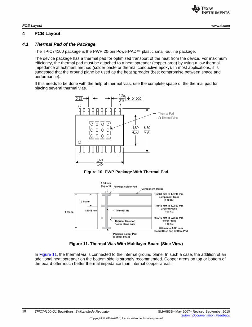
4 PCB Layout
4.1 Thermal Pad of the PackageThe TPIC74100 package is the PWP 20-pin PowerPAD™ plastic small-outline package.
The device package has a thermal pad for optimized transport of the heat from the device. For maximumefficiency, the thermal pad must be attached to a heat spreader (copper area) by using a low thermalimpedance attachment method (solder paste or thermal conductive epoxy). In most applications, it issuggested that the ground plane be used as the heat spreader (best compromise between space andperformance).
If this needs to be done with the help of thermal vias, use the complete space of the thermal pad forplacing several thermal vias.
Figure 10. PWP Package With Thermal Pad
Figure 11. Thermal Vias With Multilayer Board (Side View)
In Figure 11, the thermal via is connected to the internal ground plane. In such a case, the addition of anadditional heat spreader on the bottom side is strongly recommended. Copper areas on top or bottom ofthe board offer much better thermal impedance than internal copper areas.
18 TPIC74100-Q1 Buck/Boost Switch-Mode Regulator SLIA083B–May 2007–Revised September 2010Submit Documentation Feedback
Copyright © 2007–2010, Texas Instruments Incorporated

www.ti.com PCB Layout
4.2 Components PlacementThe placement of some of the components is critical to the converter efficiency and stability and to theEMI performance of the system. Components need to be placed according to Table 3.
Table 3. Component Placement Priority ListPriority Comment Component
• Inductor L• Output capacitors COUT and C5Vg
1 Place as close as possible to the device pins • Input capacitor Cdriver
• External Schottky diode• Vlogic capacitor
2 Place close to the device pins • Bootstrap capacitors Cboot1 and Cboot2
• Pullup resistors for AOUT and RESET• Capacitor at REST3 Least critical components• Resistance at Rmod
• Resistor divider at AIN
4.3 Traces – RoutingAll power traces should use available space for maximum with of the trace. Length of the power traces iscritical for EMI radiation. Keep connection traces of the most critical components (Priority 1 components inTable 3) as short as possible. Avoid routing through different layers. Consider the use of more than asingle via if a layer switch is required for a power trace.
4.4 Ground ConceptUsing a two-layer ground concept is recommended.
Power ground is connected with the PGND pin. All external components in the power path must connectdirectly to this power ground layer, including the inductor, input capacitor, output capacitor, 5Vg capacitor,and external Schottky diode.
The second ground layer is connected with the GND pin and the remaining GND pins of the externalcomponents, such as the capacitor at Vlogic and REST, and resistors at AIN and Rmod.
Both ground layers are connected to each other at a single location close to PGND and GND of thedevice.
19SLIA083B–May 2007–Revised September 2010 TPIC74100-Q1 Buck/Boost Switch-Mode RegulatorSubmit Documentation Feedback
Copyright © 2007–2010, Texas Instruments Incorporated

Thermal Analysis www.ti.com
5 Thermal Analysis
5.1 Terms and DefinitionsMaximum power dissipation, PD(MAX):
TJ(MAX) – Maximum allowable junction temperaturePD(MAX) = (TJ(MAX) – TA)/RθJA TA – Ambient temperature
RθJA – Thermal resistance junction to ambient
Junction temperature, TJ:
TJ – Junction temperaturePD – Power dissipationTJ = PD × RθJA + TA
TJ = (PIN – POUT) × RθJA + TA PIN – Input powerPOUT – Output power
TJ = (1 – η/100%) × PIN × RθJA + TA η – Efficiency η = (POUT/PIN) × 100%
The thermal resistance junction to ambient RθJA is specified for systems placed in still air environmentunlike the thermal resistance junction to moving air RθJMA. Several factors have a strong impact on theRθJA.
TJ = TC + (ΨJT × (PIN – POUT)) ΨJT – Junction to top of the package thermal metric
5.2 PackageThe TPIC74100 package is the PWP 20-pin PowerPAD plastic small-outline package.
For correct attachment of the thermal pad, certain trace widths, copper size, thermal vias, etc., thefollowing values have been modeled for this package:• RθJA: 32.63°C/W• ΨJT: 0.607°C/W
See the Texas Instruments application report PowerPAD™ Thermally Enhanced Package (literaturenumber SLMA002).
20 TPIC74100-Q1 Buck/Boost Switch-Mode Regulator SLIA083B–May 2007–Revised September 2010Submit Documentation Feedback
Copyright © 2007–2010, Texas Instruments Incorporated

TJ 1
100% PIN RJA TA 1 80%
100% 6.25 W 32.63oCW 100oC 140oC
P INPOUT 100%
VOUT IOUT
100% 5 V 1 A80%
100% 6.25 W
www.ti.com Thermal Analysis
5.3 Thermal Calculations ExampleApplication Conditions• Input: VIN = Vdriver = 12 V• Output: VOUT = 5 V, IOUT = 1 A• Efficiency: η = 80% (estimated)• Ambient: 100°C
Calculations
→ As explained in Section 5.1, this is a rough estimation.
→ For a closer estimation, the case temperature of the device is measured in the application.
Measured case temperature TC: TJ ≉ 132°C
TJ = TC + (ΨJT × (PIN – POUT)) ≉ 132°C + (0.607°C/W × (6.25 W – 5 W)) ≉ 132.8°C
This junction temperature is still calculated based values out of a model, but it gives an accurateestimation of the real junction temperature.
Calculations need to be continued accordingly for the external components. In particular, the capacitors forthe in and output terminal and the inductor heat themselves due to internal losses.
21SLIA083B–May 2007–Revised September 2010 TPIC74100-Q1 Buck/Boost Switch-Mode RegulatorSubmit Documentation Feedback
Copyright © 2007–2010, Texas Instruments Incorporated
Summary www.ti.com
6 SummaryThe sequence of the following questions might help evaluate the exact requirements for the individualpower-supply application. Knowing the exact requirements makes is easier to start designing with theTPIC74100. This list does not cover everything, but the most important points to be considered are:1. Will the device operate in buck mode, boost mode, or in both modes?
• May influence the selection of external components2. Is the continuous/discontinuous mode threshold important?
• Depends on load current and does influence EMI performance• Can be influenced by the inductance of the inductor
3. Is short-circuit protection required?• Inductor needs to be selected with appropriate saturation current
4. Low-power mode operation?• When to enable (verify load current conditions)?
5. What are the efficiency and EMI performance requirements?• External Schottky diode?• Resistor for modulation?• Slew rate control?• Add some fast ceramic-type capacitors?
6. Is ripple of the output voltage important?• Low-ESR output capacitor• Optional, place capacitors in parallel
7. Is the RMS current capability of the input and output capacitors sufficient?• Verify for input capacitor, especially in buck mode• Verify for output capacitor, especially in boost mode
8. Is the second output voltage at 5Vg required?• Additional output capacitor at pin 5Vg
9. Layout?• Critical components as close as possible to the device?• Power traces at maximum width?
10. Is high-temperature range required?• Thermal pad attached to heat spreader?• External components verified; self heating due to RMS current?
22 TPIC74100-Q1 Buck/Boost Switch-Mode Regulator SLIA083B–May 2007–Revised September 2010Submit Documentation Feedback
Copyright © 2007–2010, Texas Instruments Incorporated

www.ti.com References
7 ReferencesTPIC74100-Q1 Buck/Boost Switch Mode Regulator data sheet (SLIS125)
PowerPAD™ Thermally Enhanced Package (SLMA002)
IC Package Thermal Metrics (SPRA953)
Understanding Buck Power Stages in Switch-Mode Power Supplies (SLAV057)
Understanding Boost Power Stages in Switch-Mode Power Supplies (SLVA061)
23SLIA083B–May 2007–Revised September 2010 TPIC74100-Q1 Buck/Boost Switch-Mode RegulatorSubmit Documentation Feedback
Copyright © 2007–2010, Texas Instruments Incorporated

IMPORTANT NOTICE
Texas Instruments Incorporated and its subsidiaries (TI) reserve the right to make corrections, enhancements, improvements and otherchanges to its semiconductor products and services per JESD46, latest issue, and to discontinue any product or service per JESD48, latestissue. Buyers should obtain the latest relevant information before placing orders and should verify that such information is current andcomplete. All semiconductor products (also referred to herein as “components”) are sold subject to TI’s terms and conditions of salesupplied at the time of order acknowledgment.
TI warrants performance of its components to the specifications applicable at the time of sale, in accordance with the warranty in TI’s termsand conditions of sale of semiconductor products. Testing and other quality control techniques are used to the extent TI deems necessaryto support this warranty. Except where mandated by applicable law, testing of all parameters of each component is not necessarilyperformed.
TI assumes no liability for applications assistance or the design of Buyers’ products. Buyers are responsible for their products andapplications using TI components. To minimize the risks associated with Buyers’ products and applications, Buyers should provideadequate design and operating safeguards.
TI does not warrant or represent that any license, either express or implied, is granted under any patent right, copyright, mask work right, orother intellectual property right relating to any combination, machine, or process in which TI components or services are used. Informationpublished by TI regarding third-party products or services does not constitute a license to use such products or services or a warranty orendorsement thereof. Use of such information may require a license from a third party under the patents or other intellectual property of thethird party, or a license from TI under the patents or other intellectual property of TI.
Reproduction of significant portions of TI information in TI data books or data sheets is permissible only if reproduction is without alterationand is accompanied by all associated warranties, conditions, limitations, and notices. TI is not responsible or liable for such altereddocumentation. Information of third parties may be subject to additional restrictions.
Resale of TI components or services with statements different from or beyond the parameters stated by TI for that component or servicevoids all express and any implied warranties for the associated TI component or service and is an unfair and deceptive business practice.TI is not responsible or liable for any such statements.
Buyer acknowledges and agrees that it is solely responsible for compliance with all legal, regulatory and safety-related requirementsconcerning its products, and any use of TI components in its applications, notwithstanding any applications-related information or supportthat may be provided by TI. Buyer represents and agrees that it has all the necessary expertise to create and implement safeguards whichanticipate dangerous consequences of failures, monitor failures and their consequences, lessen the likelihood of failures that might causeharm and take appropriate remedial actions. Buyer will fully indemnify TI and its representatives against any damages arising out of the useof any TI components in safety-critical applications.
In some cases, TI components may be promoted specifically to facilitate safety-related applications. With such components, TI’s goal is tohelp enable customers to design and create their own end-product solutions that meet applicable functional safety standards andrequirements. Nonetheless, such components are subject to these terms.
No TI components are authorized for use in FDA Class III (or similar life-critical medical equipment) unless authorized officers of the partieshave executed a special agreement specifically governing such use.
Only those TI components which TI has specifically designated as military grade or “enhanced plastic” are designed and intended for use inmilitary/aerospace applications or environments. Buyer acknowledges and agrees that any military or aerospace use of TI componentswhich have not been so designated is solely at the Buyer's risk, and that Buyer is solely responsible for compliance with all legal andregulatory requirements in connection with such use.
TI has specifically designated certain components as meeting ISO/TS16949 requirements, mainly for automotive use. In any case of use ofnon-designated products, TI will not be responsible for any failure to meet ISO/TS16949.
Products Applications
Audio www.ti.com/audio Automotive and Transportation www.ti.com/automotive
Amplifiers amplifier.ti.com Communications and Telecom www.ti.com/communications
Data Converters dataconverter.ti.com Computers and Peripherals www.ti.com/computers
DLP® Products www.dlp.com Consumer Electronics www.ti.com/consumer-apps
DSP dsp.ti.com Energy and Lighting www.ti.com/energy
Clocks and Timers www.ti.com/clocks Industrial www.ti.com/industrial
Interface interface.ti.com Medical www.ti.com/medical
Logic logic.ti.com Security www.ti.com/security
Power Mgmt power.ti.com Space, Avionics and Defense www.ti.com/space-avionics-defense
Microcontrollers microcontroller.ti.com Video and Imaging www.ti.com/video
RFID www.ti-rfid.com
OMAP Applications Processors www.ti.com/omap TI E2E Community e2e.ti.com
Wireless Connectivity www.ti.com/wirelessconnectivity
Mailing Address: Texas Instruments, Post Office Box 655303, Dallas, Texas 75265Copyright © 2013, Texas Instruments Incorporated