towards power centric analog design - diva portal
TRANSCRIPT
Towards power centric analog design
Christer Svensson
Linköping University Post Print
N.B.: When citing this work, cite the original article.
Christer Svensson, Towards power centric analog design, 2015, IEEE Circuits and systems
magazine, 3, 44-51.
http://dx.doi.org/10.1109/MCAS.2015.2450671
©2015 IEEE. Personal use of this material is permitted. However, permission to
reprint/republish this material for advertising or promotional purposes or for creating new
collective works for resale or redistribution to servers or lists, or to reuse any copyrighted
component of this work in other works must be obtained from the IEEE.
http://ieeexplore.ieee.org/
Postprint available at: Linköping University Electronic Press
http://urn.kb.se/resolve?urn=urn:nbn:se:liu:diva-120922
1
Towards power centric analog design
Christer Svensson, Fellow, IEEE
Abstract. Power consumption of analog systems is poorly understood today, in contrast to the very well
developed analysis of digital power consumption. We show that there is good opportunity to develop also the
analog power understanding to a similar level as the digital. Such an understanding will have a large impact in
the design of future electronic systems, where low power consumption will be crucial. Eventually we may reach
a power centric analog design methodology.
Introduction.
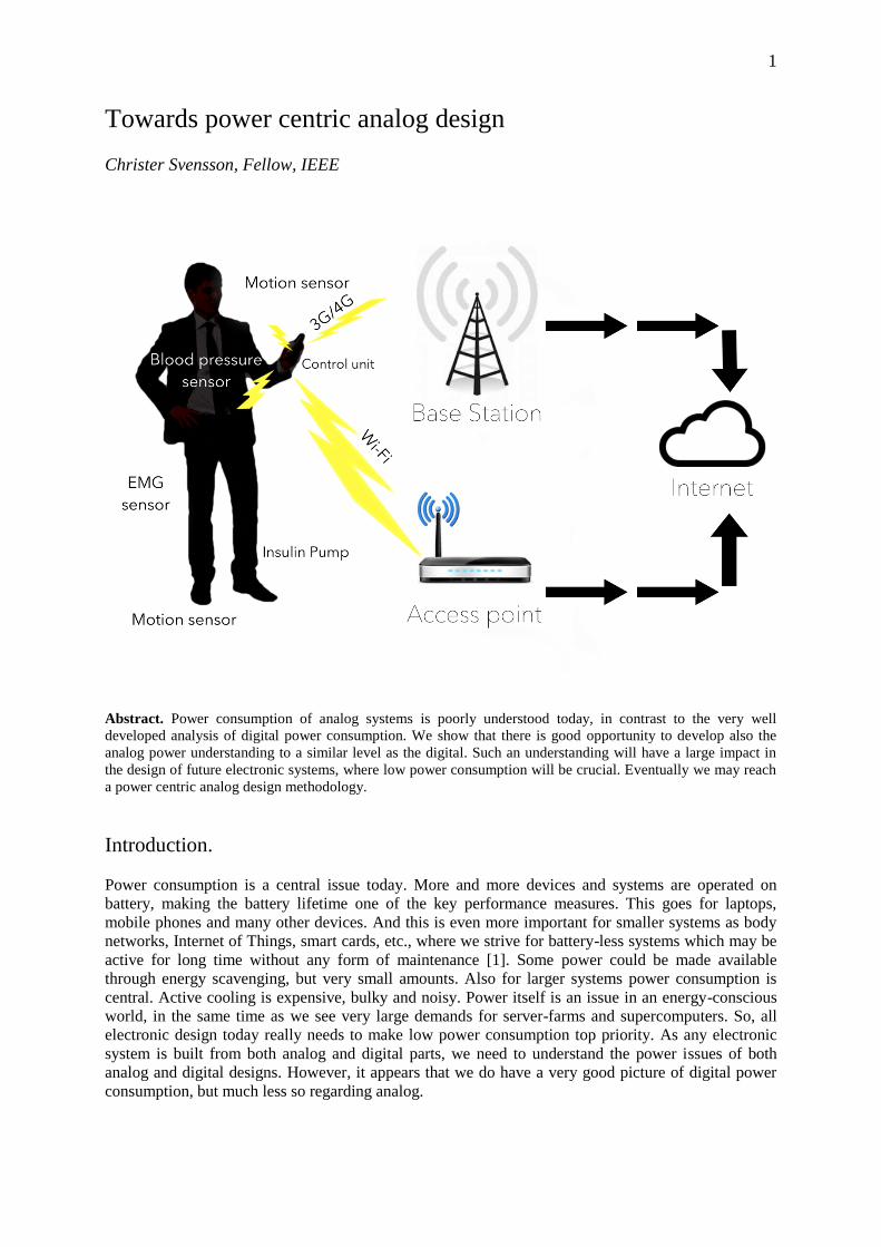
Power consumption is a central issue today. More and more devices and systems are operated on
battery, making the battery lifetime one of the key performance measures. This goes for laptops,
mobile phones and many other devices. And this is even more important for smaller systems as body
networks, Internet of Things, smart cards, etc., where we strive for battery-less systems which may be
active for long time without any form of maintenance [1]. Some power could be made available
through energy scavenging, but very small amounts. Also for larger systems power consumption is
central. Active cooling is expensive, bulky and noisy. Power itself is an issue in an energy-conscious
world, in the same time as we see very large demands for server-farms and supercomputers. So, all
electronic design today really needs to make low power consumption top priority. As any electronic
system is built from both analog and digital parts, we need to understand the power issues of both
analog and digital designs. However, it appears that we do have a very good picture of digital power
consumption, but much less so regarding analog.
2
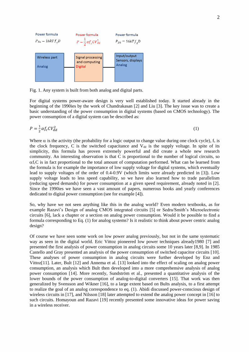
Fig. 1. Any system is built from both analog and digital parts.
For digital systems power-aware design is very well established today. It started already in the
beginning of the 1990ies by the work of Chandrakasan [2] and Liu [3]. The key issue was to create a
basic understanding of the power consumption in digital systems (based on CMOS technology). The
power consumption of a digital system can be described as:
𝑃 =1
2𝛼𝑓𝑐𝐶𝑉𝑑𝑑
2 (1)
Where is the activity (the probability for a logic output to change value during one clock cycle), fc is
the clock frequency, C is the switched capacitance and Vdd is the supply voltage. In spite of its
simplicity, this formula has proven extremely powerful and did create a whole new research
community. An interesting observation is that C is proportional to the number of logical circuits, so
fcC is in fact proportional to the total amount of computation performed. What can be learned from
the formula is for example the importance of low supply voltage for digital systems, which eventually
lead to supply voltages of the order of 0.4-0.9V (which limits were already predicted in [3]). Low
supply voltage leads to less speed capability, so we have also learned how to trade parallelism
(reducing speed demands) for power consumption at a given speed requirement, already noted in [2].
Since the 1990ies we have seen a vast amount of papers, numerous books and yearly conferences
dedicated to digital power consumption (see for example [4]).
So, why have we not seen anything like this in the analog world? Even modern textbooks, as for
example Razavi’s Design of analog CMOS integrated circuits [5] or Sedra/Smith’s Microelectronic
circuits [6], lack a chapter or a section on analog power consumption. Would it be possible to find a
formula corresponding to Eq. (1) for analog systems? Is it realistic to think about power centric analog
design?
Of course we have seen some work on low power analog previously, but not in the same systematic
way as seen in the digital world. Eric Vittoz pioneered low power techniques already1980 [7] and
presented the first analysis of power consumption in analog circuits some 10 years later [8,9]. In 1985
Castello and Gray presented an analysis of the power consumption of switched capacitor circuits [10].
These analyses of power consumption in analog circuits were further developed by Enz and
Vittoz[11]. Later, Bult [12] and Annema et al. [13] looked into the effect of scaling on analog power
consumption, an analysis which Bult then developed into a more comprehensive analysis of analog
power consumption [14]. More recently, Sundström et al., presented a quantitative analysis of the
lower bounds of the power consumption of analog-to-digital converters [15]. That work was then
generalized by Svensson and Wikner [16], to a large extent based on Bults analysis, to a first attempt
to realize the goal of an analog correspondence to eq. (1). Abidi discussed power-conscious design of
wireless circuits in [17], and Nilsson [18] later attempted to extend the analog power concept in [16] to
such circuits. Homayoun and Razavi [19] recently presented some innovative ideas for power saving
in a wireless receiver.
3
Elements of a theory of analog power consumption.
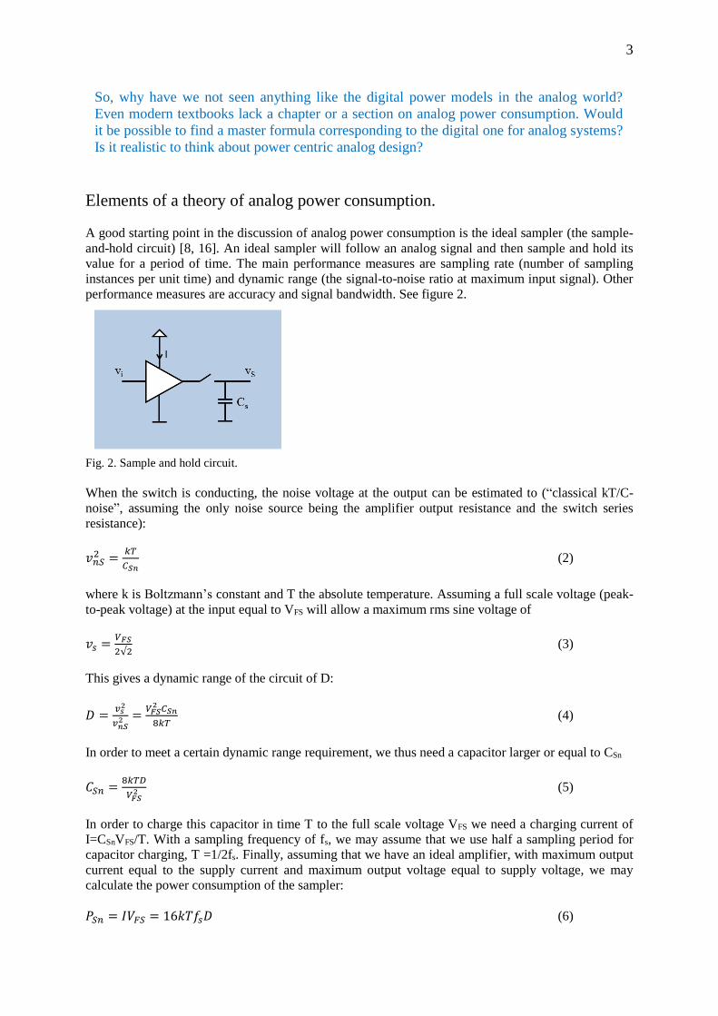
A good starting point in the discussion of analog power consumption is the ideal sampler (the sample-
and-hold circuit) [8, 16]. An ideal sampler will follow an analog signal and then sample and hold its
value for a period of time. The main performance measures are sampling rate (number of sampling
instances per unit time) and dynamic range (the signal-to-noise ratio at maximum input signal). Other
performance measures are accuracy and signal bandwidth. See figure 2.
Fig. 2. Sample and hold circuit.
When the switch is conducting, the noise voltage at the output can be estimated to (“classical kT/C-
noise”, assuming the only noise source being the amplifier output resistance and the switch series
resistance):
𝑣𝑛𝑆2 =
𝑘𝑇
𝐶𝑆𝑛 (2)
where k is Boltzmann’s constant and T the absolute temperature. Assuming a full scale voltage (peak-
to-peak voltage) at the input equal to VFS will allow a maximum rms sine voltage of
𝑣𝑠 =𝑉𝐹𝑆
2√2 (3)
This gives a dynamic range of the circuit of D:
𝐷 =𝑣𝑠2
𝑣𝑛𝑆2 =
𝑉𝐹𝑆2 𝐶𝑆𝑛
8𝑘𝑇 (4)
In order to meet a certain dynamic range requirement, we thus need a capacitor larger or equal to CSn
𝐶𝑆𝑛 =8𝑘𝑇𝐷
𝑉𝐹𝑆2 (5)
In order to charge this capacitor in time T to the full scale voltage VFS we need a charging current of
I=CSnVFS/T. With a sampling frequency of fs, we may assume that we use half a sampling period for
capacitor charging, T =1/2fs. Finally, assuming that we have an ideal amplifier, with maximum output
current equal to the supply current and maximum output voltage equal to supply voltage, we may
calculate the power consumption of the sampler:
𝑃𝑆𝑛 = 𝐼𝑉𝐹𝑆 = 16𝑘𝑇𝑓𝑠𝐷 (6)
So, why have we not seen anything like the digital power models in the analog world?
Even modern textbooks lack a chapter or a section on analog power consumption. Would
it be possible to find a master formula corresponding to the digital one for analog systems?
Is it realistic to think about power centric analog design?
4
This formula gives a good insight in analog power consumption, and may be seen as the analog
version of eq. (1). We note that it is proportional to the dynamic range of the signal and the sampling
rate (or signal bandwidth). The fact that it is proportional to kT indicates that it is bounded by thermal
noise. Furthermore, we note that this expression is independent of both technology and supply voltage,
in contrast to the digital case (eq. (1)), as also noted in [17].
So, what happens at very low dynamic ranges? Then the capacitance may become very small. What
can happen is that CSn in eq. (5) becomes less than the minimum capacitance which can be
implemented in the actual technology used. We thus need to replace CSn in the above expressions with
Cmin, the smallest capacitance which can be implemented. So, for low dynamic ranges the power
consumption will become dependent on both technology and supply voltage through Cmin and VFS:
𝑃𝑆𝑇 = 2𝑓𝑠𝐶𝑚𝑖𝑛𝑉𝐹𝑆2 (7)
We note that this expression is very similar to eq. (1), which can be interpreted as that the digital case
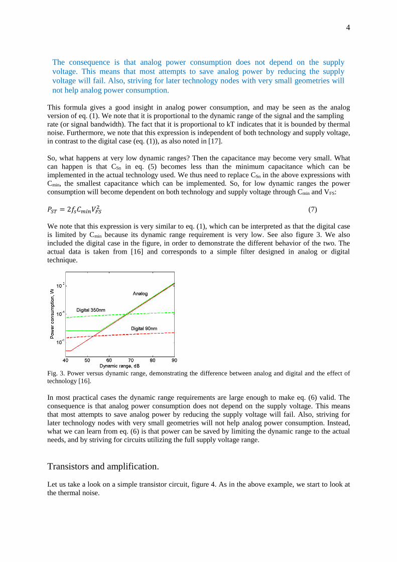
is limited by Cmin because its dynamic range requirement is very low. See also figure 3. We also
included the digital case in the figure, in order to demonstrate the different behavior of the two. The
actual data is taken from [16] and corresponds to a simple filter designed in analog or digital
technique.
Fig. 3. Power versus dynamic range, demonstrating the difference between analog and digital and the effect of
technology [16].
In most practical cases the dynamic range requirements are large enough to make eq. (6) valid. The
consequence is that analog power consumption does not depend on the supply voltage. This means
that most attempts to save analog power by reducing the supply voltage will fail. Also, striving for
later technology nodes with very small geometries will not help analog power consumption. Instead,
what we can learn from eq. (6) is that power can be saved by limiting the dynamic range to the actual
needs, and by striving for circuits utilizing the full supply voltage range.
Transistors and amplification.
Let us take a look on a simple transistor circuit, figure 4. As in the above example, we start to look at
the thermal noise.
The consequence is that analog power consumption does not depend on the supply
voltage. This means that most attempts to save analog power by reducing the supply
voltage will fail. Also, striving for later technology nodes with very small geometries will
not help analog power consumption.

5
Fig. 4. Simple transistor amplifier.
For an MOS transistor we normally express the drain noise current in terms of transistor
transconductance, gm as:
𝑖𝑑𝑛2 = 4𝑘𝑇𝛾𝑔𝑚𝐵𝑛 (8)
where is a noise factor and Bn is the system noise bandwidth [16]. In the following we neglect noise
contributions from other sources than the transistor drain current (as the drain current noise normally
dominates). The output noise voltage, 𝑣𝑑𝑛 = 𝑅𝑖𝑑𝑛. Again, assuming that the output full scale voltage
is VFS, corresponding to a maximum output as eq. (3), we may express the dynamic range, D, as:
𝐷 =𝑣𝑆2
𝑣𝑑𝑛2 =
𝑉𝐹𝑆2 𝑔𝑚
32𝑘𝑇𝛾𝐴𝑣2𝐵𝑛
(9)
where we introduced the DC gain of this stage, Av = gmR. From eq. (9) we may now calculate the gm
needed to reach the dynamic range, D:
𝑔𝑚 =32𝑘𝑇𝛾𝐴𝑣
2𝐵𝑛
𝑉𝐹𝑆2 𝐷 (10)
To achieve a certain transconductance, gm, we need to supply the transistor with a bias current ID =
gmVeff, where we have introduced the parameter Veff (of the order of 25 to 500 mV, see below). Using
ID together with the supply voltage, again assumed to be VFS, we can calculate the power consumption
as:
𝑃𝑇𝑛 = 32𝑘𝑇𝛾𝐴𝑣2𝐵𝑛
𝑉𝑒𝑓𝑓
𝑉𝐹𝑆𝐷 (11)
We may note large similarities to eq. (6), particularly considering the close relation between sampling
frequency, fs, and bandwidth, Bn. Noting that fs≈2Bn (for Nyquist sampling) makes 32Bn equal to 16fs,
and eq. (11) differ from eq. (6) only through Av2 and Veff/VFS. The first of these factors indicates that
voltage gain comes at a power cost and the second factor indicates that part of this cost is mitigated if
we can choose a small value of Veff.
Just as eq. (6), also eq. (11) is independent of the technology used. However, again this is not entirely
true. In order to understand this we need to include the capacitive load of the transistor, CLn, assumed
parallel to R. CLn will control the noise bandwidth through Bn=1/4RCLn (noise bandwidth of a single
pole low-pass filter). Inserting this expression into eq. (9) and solving for CLn gives:
𝐶𝐿𝑛 =8𝑘𝑇𝛾𝐴𝑣
𝑉𝐹𝑆2 𝐷 (12)

6
which is similar to eq. (5). So, if CLn is less than the smallest capacitance that can be implemented, we
need to replace CLn with Cmin as before. To keep the same bandwidth and gain we need gm=4AvCminBn
which leads to a power consumption of:
𝑃𝑇𝑇 = 4𝐵𝑛𝐶𝑚𝑖𝑛𝑉𝑒𝑓𝑓𝑉𝐹𝑆𝐴𝑣 (13)
which is similar to eq. (7). So for low dynamic range also the transistor circuit has a power
consumption which depends on technology (Cmin) and supply voltage (VFS).
Let us now discuss the Veff parameter used above. Veff, is defined as [15]:
𝑉𝑒𝑓𝑓 =𝐼𝐷
𝑔𝑚 (14)
For a classical long channel MOST in strong inversion Veff=(VG-VT)/2, where VG and VT are the gate
voltage and threshold voltage respectively. For weak inversion, that is for VG<VT, Veff=mkT/q, with m
slightly larger than 1. For a modern submicron MOST Veff tends to fall above these values, see figure
7 in [15]. We could also note that bipolar transistors exhibits Veff=kT/q.
Returning to the MOS transistor and the formula above, we can conclude that small Veff is preferred to
save power. But there are some constraints to how we can choose Veff. First transistor speed depends
on gate bias, so a low Veff corresponding to a low VG leads to reduced speed. Transistor speed can be
characterized by fT, the frequency at which the transistor current gain has fallen to one. In figure 7 in
[15] we note quite a difference between two process nodes. In a 350nm node we need to keep quite a
large Veff to keep transistor speed, whereas in a 90nm node we do not gain much speed above
VG=100mV corresponding to Veff=100mV. So, deep submicron technologies easily combine low
power and high speed.
Second, high input voltage amplitude is not compatible with very low Veff. If the input voltage
amplitude is large compared to Veff, then we can expect a highly nonlinear response of the transistor.
For example, for an input voltage swing of VFSin=Veff (where VFSin is the peak-to-peak gate voltage),
the transistor current will vary roughly between IDC/2 and 3IDC/2 (IDC is the DC drain bias). Thus
choosing Veff larger or equal to the peak-to-peak gate voltage is a reasonable first attempt to keep the
circuit linear. Bult derived a more strict relationship between VFSin, Veff and the second order
distortion, HD2, HD2=VFSin/2Veff, valid for MOSTs in strong inversion [20].
Including more circuit specifications.
In the above description only dynamic range given by thermal noise and speed is considered. We
showed initially that the dynamic range requirement leads to a requirement on the minimum load
capacitance. We then showed how this capacitance, in combination with a speed requirement leads to
a lower bound of power consumption.
Bult [14] used the same scheme as this one, but extended it to include more circuit specifications. He
showed that not only thermal noise, but also 1/f noise and circuit matching will put demands on the
capacitance. So in practice several specifications will control the load capacitance. Then he showed
that not only bandwidth or sampling time will affect the power consumption at a given load
capacitance, but also slew rate, distortion and settling.
Still, however, the basic scheme above is always valid. Power consumption can be understood in terms
of a minimum capacitance requirement, and the current required driving that capacitance. The
capacitance is given by technology, thermal noise, 1/f –noise, and matching (in terms of offset or gain
matching) [14, 15, 16]. And the current is controlled by this minimum capacitance, combined with the
7
requirements on speed (in terms of bandwidth, sampling rate or slew rate), settling accuracy, and
distortion (in terms of second order or third order distortion with or without feedback) [14, 15].
Radio frequency circuits.
The above discussion mainly treats low frequency or wide-band circuits. The large difference
compared to radio frequency circuits is that radio frequency circuits normally utilize inductors.
Therefore inductor performance will be an important additional factor for circuit performance and
power consumption.
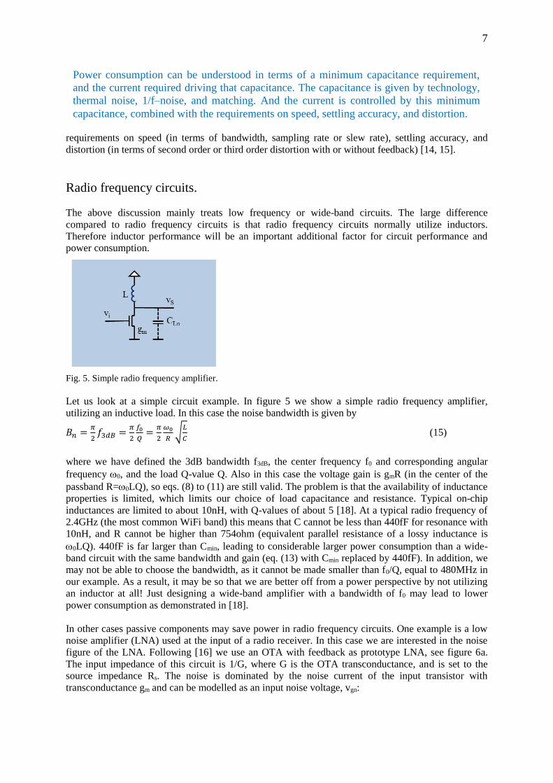
Fig. 5. Simple radio frequency amplifier.
Let us look at a simple circuit example. In figure 5 we show a simple radio frequency amplifier,
utilizing an inductive load. In this case the noise bandwidth is given by
𝐵𝑛 =𝜋
2𝑓3𝑑𝐵 =
𝜋
2
𝑓0
𝑄=
𝜋
2
𝜔0
𝑅√𝐿
𝐶 (15)
where we have defined the 3dB bandwidth f3dB, the center frequency f0 and corresponding angular
frequency 0, and the load Q-value Q. Also in this case the voltage gain is gmR (in the center of the
passband R=0LQ), so eqs. (8) to (11) are still valid. The problem is that the availability of inductance
properties is limited, which limits our choice of load capacitance and resistance. Typical on-chip
inductances are limited to about 10nH, with Q-values of about 5 [18]. At a typical radio frequency of
2.4GHz (the most common WiFi band) this means that C cannot be less than 440fF for resonance with
10nH, and R cannot be higher than 754ohm (equivalent parallel resistance of a lossy inductance is
0LQ). 440fF is far larger than Cmin, leading to considerable larger power consumption than a wide-
band circuit with the same bandwidth and gain (eq. (13) with Cmin replaced by 440fF). In addition, we
may not be able to choose the bandwidth, as it cannot be made smaller than f0/Q, equal to 480MHz in
our example. As a result, it may be so that we are better off from a power perspective by not utilizing
an inductor at all! Just designing a wide-band amplifier with a bandwidth of f0 may lead to lower
power consumption as demonstrated in [18].
In other cases passive components may save power in radio frequency circuits. One example is a low
noise amplifier (LNA) used at the input of a radio receiver. In this case we are interested in the noise
figure of the LNA. Following [16] we use an OTA with feedback as prototype LNA, see figure 6a.
The input impedance of this circuit is 1/G, where G is the OTA transconductance, and is set to the
source impedance Rs. The noise is dominated by the noise current of the input transistor with
transconductance gm and can be modelled as an input noise voltage, vgn:
Power consumption can be understood in terms of a minimum capacitance requirement,
and the current required driving that capacitance. The capacitance is given by technology,
thermal noise, 1/f–noise, and matching. And the current is controlled by this minimum
capacitance, combined with the requirements on speed, settling accuracy, and distortion.
8
𝑣𝑔𝑛2 =
𝑖𝑑𝑛2
𝑔𝑚2 =
4𝑘𝑇𝛾𝐵𝑛
𝑔𝑚 (16)
And the noise figure can be expressed as
𝐹 = 1 +𝑣𝑔𝑛2
𝑣𝑠𝑛2 = 1 +
𝛾
𝑔𝑚𝑅𝑠 (17)
Fig. 6. a) prototype LNA, and b) prototype LNA with impedance transformer.
where vsn is the noise voltage of the source resistance Rs, vsn
2=4kTRsBn. So, a certain requirement on
noise figure becomes a requirement on gm, which then leads to a certain power consumption through
P=gmVeffVdd as above.
How can we save power in this case? We note that gmRs appear in eq. (17), so if we can increase Rs we
may decrease gm for the same noise figure. And Rs can be increased by a passive impedance
transformer at the LNA input [17, 18, 19]. In [18] it was shown that an impedance transformer based
on an external inductance (figure 6b) will have an impedance transformation ratio equal to the Q-value
of the external inductance, which may be about 35 at 2.4GHz. An external inductance may therefore
lead to a power reduction of 35x at a given noise figure. More drastic solution is to replace the LNA
by a passive transformer, directly followed by a passive mixer [19]. An extended discussion of power-
conscious design of radio frequency circuits can be found in [17].
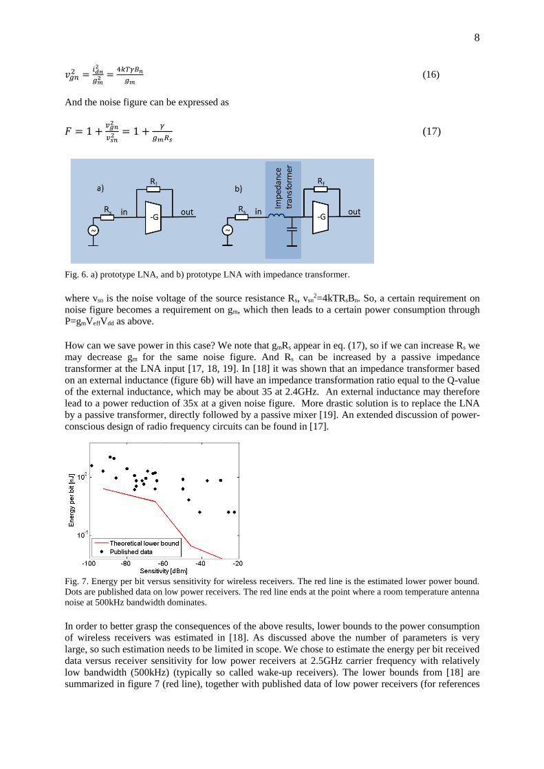
Fig. 7. Energy per bit versus sensitivity for wireless receivers. The red line is the estimated lower power bound.
Dots are published data on low power receivers. The red line ends at the point where a room temperature antenna
noise at 500kHz bandwidth dominates.
In order to better grasp the consequences of the above results, lower bounds to the power consumption
of wireless receivers was estimated in [18]. As discussed above the number of parameters is very
large, so such estimation needs to be limited in scope. We chose to estimate the energy per bit received
data versus receiver sensitivity for low power receivers at 2.5GHz carrier frequency with relatively
low bandwidth (500kHz) (typically so called wake-up receivers). The lower bounds from [18] are
summarized in figure 7 (red line), together with published data of low power receivers (for references
9
see [18]). We note three sections of the bound curve. For very low sensitivities (on the right) the
power bound is given by the baseband amplifier. For the mid part the power bound is related to the
detector (here an active nonlinear element), utilizing an input impedance transformer as discussed
above. In these two sections the most efficient receiver utilizes just an envelope detector and a
baseband amplifier. For the leftmost sector of the red curve a low noise amplifier is added to the
architecture. In no case a superheterodyne architecture is preferred from a power perspective.
Inductors are beneficiary only in the input impedance transformer.
Analog-to-digital converters.
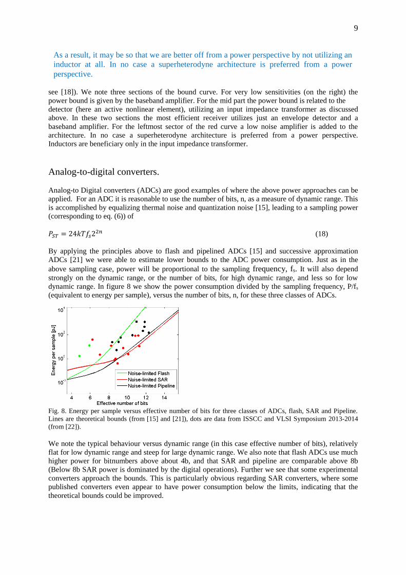
Analog-to Digital converters (ADCs) are good examples of where the above power approaches can be
applied. For an ADC it is reasonable to use the number of bits, n, as a measure of dynamic range. This
is accomplished by equalizing thermal noise and quantization noise [15], leading to a sampling power
(corresponding to eq. (6)) of
𝑃𝑆𝑇 = 24𝑘𝑇𝑓𝑠22𝑛 (18)
By applying the principles above to flash and pipelined ADCs [15] and successive approximation
ADCs [21] we were able to estimate lower bounds to the ADC power consumption. Just as in the
above sampling case, power will be proportional to the sampling frequency, fs. It will also depend
strongly on the dynamic range, or the number of bits, for high dynamic range, and less so for low
dynamic range. In figure 8 we show the power consumption divided by the sampling frequency, P/fs
(equivalent to energy per sample), versus the number of bits, n, for these three classes of ADCs.
Fig. 8. Energy per sample versus effective number of bits for three classes of ADCs, flash, SAR and Pipeline.
Lines are theoretical bounds (from [15] and [21]), dots are data from ISSCC and VLSI Symposium 2013-2014
(from [22]).
We note the typical behaviour versus dynamic range (in this case effective number of bits), relatively
flat for low dynamic range and steep for large dynamic range. We also note that flash ADCs use much
higher power for bitnumbers above about 4b, and that SAR and pipeline are comparable above 8b
(Below 8b SAR power is dominated by the digital operations). Further we see that some experimental
converters approach the bounds. This is particularly obvious regarding SAR converters, where some
published converters even appear to have power consumption below the limits, indicating that the
theoretical bounds could be improved.
As a result, it may be so that we are better off from a power perspective by not utilizing an
inductor at all. In no case a superheterodyne architecture is preferred from a power
perspective.
10
The parameters used in calculating the bounds in figure 8 corresponds to a 90nm technology [15, 21],
whereas the experimental data refers to 28nm to 180nm technologies. The experimental data covers
sampling frequencies between 4kHz and 5GHz, and are taken from [22].
How to utilize this knowledge?
So, if we eventually understand the relation between power consumption and circuit performance, how
to utilize this knowledge? One way to utilize it is to use the understanding to estimate the lower
bounds of power consumption of a particular class of circuits. Comparing these lower bounds to actual
power consumption, we may discover areas with large prospect for improvements, and therefore
promising areas of research or product development. For example, figure 7 suggests that
improvements can be expected for low sensitivity wireless receivers.
Another way to utilize this knowledge is by starting a new circuit design project by estimating the
power consumption of the circuit, based on its specifications. By using this estimate as a design target,
there will be a good chance to arrive to a power-optimal solution. An example of this thinking is found
in [23]. Similarly, if specifications of a product are changed (new technology available, changed
requirements, etc.) it is possible to estimate the power consumption of an upgraded design and thus to
judge if an upgrade is worth the effort.
A third application is to compare different solutions to a given problem from a power consumption
perspective, including comparison between digital and analog solutions, or comparison between
different architectures.
Future work.
Analog circuits are far more diverse that digital circuits. Therefore it is very difficult to formulate a
general description of the power consumption of analog circuits. Still, we believe that the descriptions
above, together with the ideas formulated in [14], could be the first elements of such a general
description, although many aspects of analog circuits are left to be investigated.
Examples of important topics to be investigated are linearity, matching, and RF passives. Regarding
linearity we need to relate power consumption to various linearity requirements, as HD2/HD3, THD,
IP2/IP3, SFDR etc. We also need to understand the power cost for linearity improvement through
feedback or other circuit tricks. Matching requirements are sometimes quite expensive in power,
particularly regarding offset [14]. Therefore we need compensating techniques, as offset
compensation, offset and gain calibration, etc., and we need to understand the power cost for such
techniques. Contemporary AD-converters often use various digital calibration or error correction
techniques to mitigate matching errors. In these cases also the power consumption of the digital
functions must be considered. As discussed above RF passives may have a large impact on power, but
the use of passives is not governed by power alone. Other aspects, as radio receiver selectivity, or
suppression of unwanted signals, are also essential. Again, all requirements must be included when
optimizing for power, which calls for a very good understanding of the whole problem. So, there is a
lot to do!
Conclusion.
It is possible to develop a generic theory of power consumption in analog circuits, similarly to what is
available for digital circuits. We demonstrated the usefulness for such a theory in terms of the
development and utilization of lower bounds to power consumption or in terms of comparisons
between different system architectures. Still, what we have is just the first steps towards a complete

11
theory, indicating a fruitful future research area. Based on these and future results we may approach a
power centric analog design methodology, similarly to what we have in the digital domain.
References.
[1] V. Sai and M. H. Mickle, “Exploring Energy Efficient Architectures in Passive Wireless Nodes for IoT
Applictions”, IEEE Circuits and Systems Magazine, Second quarter 2014, pp. 48-54, May 2014.
[2] A. Chandrakasan, S. Sheng, and R. Brodersen, ” Low power CMOS digital design”. IEEE Journal of Solid-
State Circuits, vol. 27, issue 4, pp. 473–484, April 1992.
[3] D. Liu and C. Svensson, “Trading speed for low power by choice of supply and threshold voltages”, IEEE
Journal of Solid-State Circuits, vol. 28, issue 1, pp 10-17, January 1993.
[4] Low-Power Electronic Design, C. Piguet, ed., CRC Press, 2005.
[5] B. Razavi, Design of analog CMOS integrated circuits, McGraw Hill, 2000.
[6] A. S. Sedra and K.C.Smith, Microelectronic circuits, Oxford University Press, 2011.
[7] E. Vittoz, “Micropower IC”, In IEEE European Solid-State Circuits Conference 1980, vol. 2, pp. 174–189,
September 1980.
[8] E. Vittoz, “Future of analog in the VLSI environment”, In IEEE International Symposium on Circuits and
Systems 1990, vol. 2, pp. 1372–1375, May 1990.
[9] E. Vittoz, “Low-power design: Ways to approach the Limits”, In 41st IEEE International Solid-State Circuits
Conference, Digest of Technical Papers., pp. 14–18, February 1994.
[10] R. Castello and P. R. Gray, “Performance Limitations in Switched-Capacitor Filters”, IEEE Transactions of
Circuits and Systems, vol. 32, issue 9, pp. 865-876, September 1985.
[11] C. C. Enz and E. A. Vittoz, “CMOS low-power analog circuit Design”, Designing Low Power Digital
Systems, Emerging Technologies, pp. 79–133, May 1996.
[12] K. Bult, “Analog design in deep sub-micron CMOS”, In Proceedings of the 26th European Solid-State
Circuits Conference, ESSCIRC’00, pp. 126–132, Sept. 2000.
[13] A.-J. Annema, B. Nauta, R. van Langevelde, and H. Tuinhout, “Analog circuits in ultra-deep-submicron
CMOS”, IEEE Journal of Solid-State Circuits, vol. 40, issue 1, pp. 132–143, January 2005.
[14] K. Bult, "The effect of technology scaling on power dissipation in analog circuits", in Analog Circuit
Design. Springer, 2006, pp. 251-294.
[15] T. Sundstrom, B. Murmann and C. Svensson, ”Power dissipation bounds for high-speed Nyquist analog-to-
digital converters”, IEEE Transactions on Circuits and Systems I: Regular Papers, vol. 56, issue 3, pp. 509–518,
March 2009.
[16] C. Svensson and J. J. Wikner, ”Power consumption of analog circuits: a tutorial”, Analog Integrated
Circuits and Signal Processing, vol. 65, issue 2, pp. 171-184, November 2010.
[17] A. Abidi, G. Pottie, and W. Kaiser, “Power-conscious design of wireless circuits and systems”, Proceedings
of the IEEE, vol. 88, pp. 1528–1545, October 2000.
[18] E. Nilsson and C. Svensson, “Power Consumption of Integrated Low-Power Receivers”, IEEE Journal on
Emerging and Selected Topics in Circuits and Systems, Vol. 4, Issue 3, pp. 273-283, September 2014.
12
[19] A. Homayoun and B. Razavi, “A Low Power CMOS Receiver for 5GHz WLAN”, IEEE Journal of Solid-
State Circuits, vol. 50, issue 3, pp. 630–643, March 2015.
[20] K. Bult, “Distortion”, lecture notes, unpublished.
[21] D. Zhang, C. Svensson and A. Alvandpour, ”Power consumption bounds for SAR ADCs”, 20th European
Conference on Circuit Theory and Design (ECCTD), pp. 577-580, August 2011.
[22] B. Murmann, “ADC performance survey 1997-2014. [online].
http://www.stanford.edu/murmann/adcsurvey.html.
[23] F. Ul Amin, C. Svensson and M. Gustavsson, “Low-Power, High-Speed, and Low-Noise X-Ray Readout
Channel in 0.18μm CMOS”, Proceedings of the 17th International Conference Mixed Design of Integrated
Circuits and Systems (MIXDES), pp. 289 – 293, June 2010.
Christer Svensson (F’03) is Professor Emeritus of Electronic devices at Linköping University. He received the
M.S. and Ph.D. degrees from Chalmers University, Sweden, in 1965 and 1970 respectively. He joined Linköping
University 1978, where he since 1983 is professor in Electronic devices. As professor he initiated a new research
group on integrated circuit design. He pioneered the fields of high-speed CMOS design in 1987, and low-power
CMOS 1993. His present interests are high performance and low power analog and digital CMOS circuit
techniques for computing, wireless systems and sensors. Svensson has published more than 180 papers in
international journals and conferences and holds ten patents. He was awarded the Solid-State Circuits Council
Best Paper Award for 1988-89. He is a member of the Royal Swedish Academy of Sciences and the Royal
Swedish Academy of Engineering Sciences. He cofounded several companies, for example SiCon
Semiconductor, Switchcore (publ.) and Coresonic.