towards a model for impact of technology evolution on...
TRANSCRIPT
Towards a Model for Impact of Technology Evolution on Wafer-Level
ESD Damage Susceptibility
Lou DeChiaro Terry Welsher
www.dangelmayer.com
Copyright © 2007 Dangelmayer Associates 2
Setting the Stage
• Wafer level ESD damage has long been a mystery• Investigators lacked tools to detect events in situ• Often yields were low and any ESD was masked by other
handling-induced errors• Early robotic equipment was more sensitive than the wafers• Electrostatic attraction (ESA) emerged as the more
significant problem• Some ESA mitigation techniques probably also reduce ESD
risk• ESD vulnerability very dependent on specific wafer
construction• Attitudes range widely from indifference to serious concern• Little being done, few actual investigations
Copyright © 2007 Dangelmayer Associates 3
Some Prior Work
• Early processing at AT&T (1970-1980) – Failures at wafer level a major problem
• Burr Brown (1991 EOS/ESD Symposium) - “streaming potential” causes ESD damage at wafer rinse
• Seagate (1998 EOS/ESD symposium) – Damage to MR Heads at Ion Milling (not really ESD but vulnerabilities may be similar)
• Jacob & Nicoletti (2006 IEEE Trans Dev Mat Rel) – Allude to ESD damage “directly to chip surface”

Copyright © 2007 Dangelmayer Associates 4
Some Prior Work
• Infineon (2006 EOS/ESD Symposium) - claim no damage at wafer saw
• Infineon 2007 Future-Fab article – On-going efforts to eliminate ESD events driven by fear of device damage but no direct evidence cited
• Damage at wafer saw – Direct experience

Copyright © 2007 Dangelmayer Associates 5
Wafer Saw ESD Events
Wafer Saw 6351 – CO2 bubbler on
Wafer Saw 6351 – CO2 bubbler off
Events captured by ESD event detector

Copyright © 2007 Dangelmayer Associates 6
ESD Threshold Populations including high speed applications
ESD Populations including high speed applications
00.00010.00020.0003
0.00040.00050.00060.0007
0 1000 2000 3000 4000 5000 6000
ESD Threshold (volts)
Rel
ativ
e Fr
eque
ncy 1996
20022008HS 1996HS 2002HS 2008
Distribution becoming bimodal
Copyright © 2007 Dangelmayer Associates 7
0
500
1000
1500
2000
2500
1980 1985 1990 1995 2000 2005 2010
HBMCDMMM
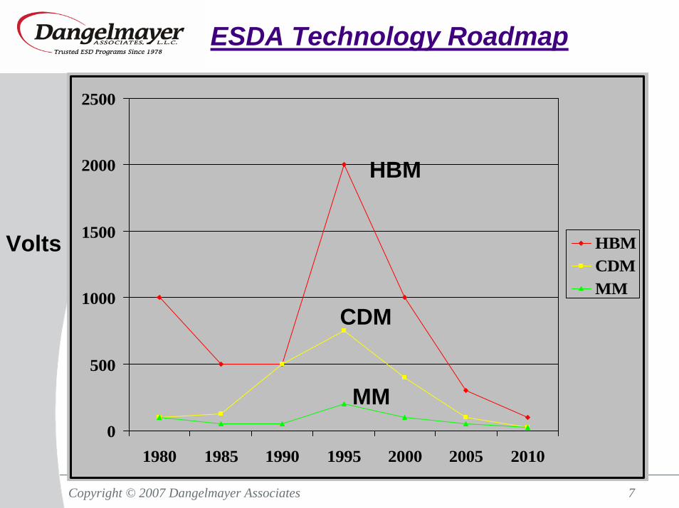
ESDA Technology Roadmap
Volts
HBM
CDM
MM
Copyright © 2007 Dangelmayer Associates 8
Wafer Level ESD Model
• Details of the Model• Results• Limitations and Improvements

Copyright © 2007 Dangelmayer Associates 9
Objectives• Create a framework for predicting voltage levels on
wafers due to ESD in the front-end environment• Estimate how geometric changes in wafer
construction affect ESD vulnerability• Identify processing and feature scale information
needed to improve estimates
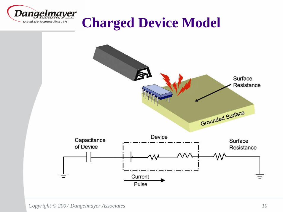
Strategy• Develop a computer model for typical wafer-level
ESD event• Base model on a charged-device model (CDM)
scenario (wafer grounded in a static field)
Wafer-Level ESD Model
Copyright © 2007 Dangelmayer Associates 10
Charged Device Model

Copyright © 2007 Dangelmayer Associates 11
FCDM Simulator

Copyright © 2007 Dangelmayer Associates 12
Model Description• Integrated Wafer-Simulator CDM Model
– Wafer modeled as an array of capacitances with respect to the field source
• Technology evolution related to this capacitance variation– Feature-to-feature and feature-to backside capacitances are
small and neglected for this analysis– Feature-to-feature potential differences used as an indicator
of device failure– Thermal effects were not considered since any significant
heating would be on back side of wafer well away from sensitive features
• Changes to new materials (e.g., ZrO2) are not included
• The following lumped-elements were used in circuit model for the CDM generator – Nonlinear arc resistance– Ground probe inductance
Copyright © 2007 Dangelmayer Associates 13
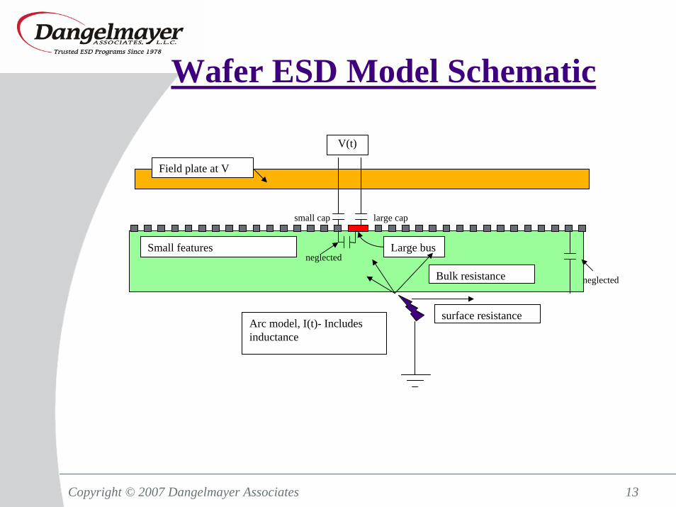
Wafer ESD Model Schematic
Field plate at V
Arc model, I(t)- Includes inductance
Small features Large bus
Bulk resistance
V(t)
surface resistance
small cap large cap
neglected
neglected
Copyright © 2007 Dangelmayer Associates 14
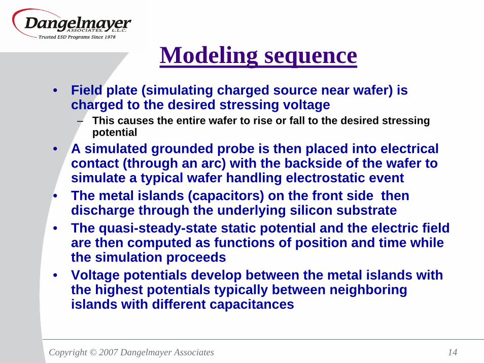
Modeling sequence• Field plate (simulating charged source near wafer) is
charged to the desired stressing voltage– This causes the entire wafer to rise or fall to the desired stressing
potential• A simulated grounded probe is then placed into electrical
contact (through an arc) with the backside of the wafer to simulate a typical wafer handling electrostatic event
• The metal islands (capacitors) on the front side then discharge through the underlying silicon substrate
• The quasi-steady-state static potential and the electric field are then computed as functions of position and time while the simulation proceeds
• Voltage potentials develop between the metal islands with the highest potentials typically between neighboring islands with different capacitances

Copyright © 2007 Dangelmayer Associates 15
Failure Mechanism
• A fast transient leads to voltage potential between features
• Sufficiently high voltage for sufficient duration initiates Fowler-Nordheim (F-N) tunneling*
• Failure occurs when cumulative charge trapping exceeds a certain level defined as Qbd
*See S. Sze, Physics of Semiconductor Devices, Second Edition, p497.
Copyright © 2007 Dangelmayer Associates 16
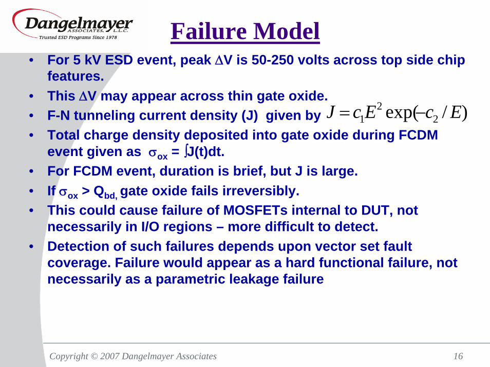
Failure Model• For 5 kV ESD event, peak ΔV is 50-250 volts across top side chip
features.• This ΔV may appear across thin gate oxide.• F-N tunneling current density (J) given by• Total charge density deposited into gate oxide during FCDM
event given as σox = ∫J(t)dt. • For FCDM event, duration is brief, but J is large.• If σox > Qbd, gate oxide fails irreversibly.• This could cause failure of MOSFETs internal to DUT, not
necessarily in I/O regions – more difficult to detect.• Detection of such failures depends upon vector set fault
coverage. Failure would appear as a hard functional failure, notnecessarily as a parametric leakage failure
)/exp( 22
1 EcEcJ −=
Copyright © 2007 Dangelmayer Associates 17
Ignoring Inter-feature Capacitance
• For this model, inter-feature capacitances are paralleled by inter-feature resistance of 1/(g*mesh spacing). This resistance is about 0.8 ohm.
• Consider a 0.8 ohm resistor in parallel with an inter-feature capacitor of 0.1 pF. Compare resistor conduction current (ΔV/R) & capacitor displacement current (Cdv/dt).
• For 5 kV event, peak Icond = 25 A.; peak Idis=0.4 A.• Conduction current dominates capacitor
displacement current. So, we’ve ignored inter-feature capacitance.
• Addition of inter-feature capacitance to model is always possible at client request.
Copyright © 2007 Dangelmayer Associates 18
Simulation Runs
• Variables explored– Large and small capacitance values– Bulk wafer conductivity– Back surface conductivity– Stressing voltage– Zap location
• Fixed quantities– Wafer thickness– Feature spacing– Arc model with fixed voltage/length

Copyright © 2007 Dangelmayer Associates 19
Typical waveform
Current waveform5000 volt
-30
-25
-20
-15
-10
-5
00.000 0.500 1.000 1.500 2.000
time (nsec)
arc
curr
ent (
Am
ps)
Copyright © 2007 Dangelmayer Associates 20
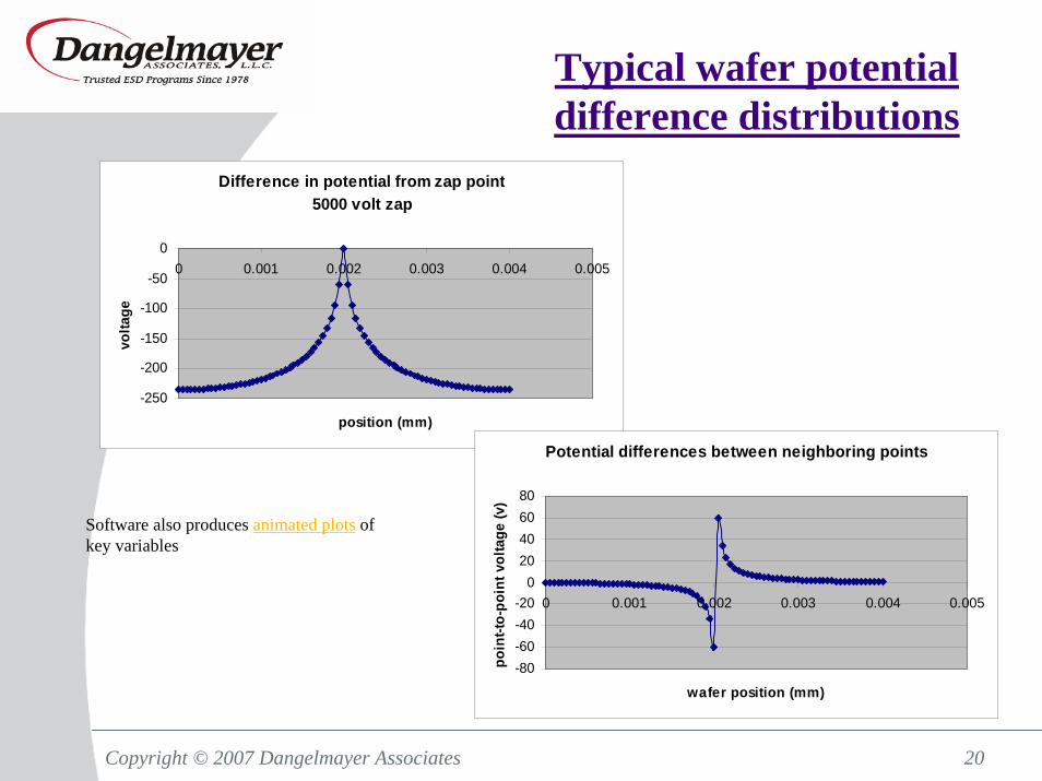
Typical wafer potential difference distributions
Difference in potential from zap point5000 volt zap
-250
-200
-150
-100
-50
00 0.001 0.002 0.003 0.004 0.005
position (mm)
volta
ge
Potential differences between neighboring points
-80-60-40-20
020406080
0 0.001 0.002 0.003 0.004 0.005
wafer position (mm)
poin
t-to-
poin
t vol
tage
(v)
Software also produces animated plots ofkey variables
Copyright © 2007 Dangelmayer Associates 21
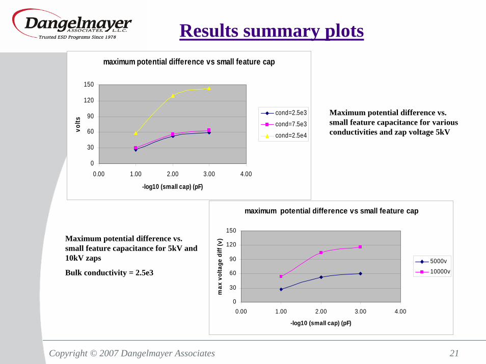
Results summary plotsmaximum potential difference vs small feature cap
0
30
60
90
120
150
0.00 1.00 2.00 3.00 4.00
-log10 (small cap) (pF)
volts
cond=2.5e3
cond=7.5e3
cond=2.5e4
maximum potential difference vs small feature cap
0
30
60
90
120
150
0.00 1.00 2.00 3.00 4.00
-log10 (small cap) (pF)
max
vol
tage
diff
(v)
5000v10000v
Maximum potential difference vs. small feature capacitance for 5kV and 10kV zaps
Bulk conductivity = 2.5e3
Maximum potential difference vs. small feature capacitance for various conductivities and zap voltage 5kV

Copyright © 2007 Dangelmayer Associates 22
Summary and Conclusions
• Changes in relative capacitance with respect to charge source of neighboring features could have significant effect on voltage differentials between features on a die
• Maximum voltage potentials appear for ~100 picoseconds at or near the time of current peak and at point of larger capacitance
• Maximum feature-to-feature potentials roughly scale with zap voltage

Copyright © 2007 Dangelmayer Associates 23
Summary and Conclusions(cont.)
• Need to relate small-to-large capacitance range to technology evolution
• Failures would be difficult to detect based on current test techniques since they would be internal, depend on test coverage
• Status: These results suggest that relatively high voltages can be developed on wafer-like structures. Further work is required to firmly establish the “calibration” of the results using actual Qbd, capacitances and conductivities