touch through glass with sharp® lcd design guide (rev. b)
TRANSCRIPT
Copyright © 2016, Texas Instruments Incorporated
TIDA-00494
CAPTIVATE-FR2633
20-p
in f
emal
e (t
o p
rog
ram
mer
PC
B)
I2C
UART
IRQ
SYNC
SPI-BI-WIRE
+3.3V(VCC_LDO)
LCD
CapTIvate I/O(4)
GPIO(4)
SPI
1TIDUBZ4B–July 2016–Revised May 2019Submit Documentation Feedback
Copyright © 2016–2019, Texas Instruments Incorporated
Touch Through Glass With Sharp® LCD Reference Design
Design Guide: TIDA-00494Touch Through Glass With Sharp® LCD Reference Design
DescriptionA human machine interface (HMI) is an essential partof process plants because it is one of the major waysthrough which humans and machines interact. TheTIDA-00494 reference design offers an HMI solutionfor harsh and hazardous area applications. In processplants, operators are required to interact with keypadsfor programming functions, encapsulated in explosiveproof screw-on metallic enclosures with thick glasswindows for local readouts through a liquid crystaldisplay (LCD).
The TIDA-00494 TI Design uses MSP430™microcontrollers (MCU) with TI CapTIvate™technology. This reference design allows the operatorto interact with the controller without the need ofopening the enclosure saving time by avoiding workpermit or plant shutdown., read the results from anLCD, and get notified with a light-emitting diode (LED)with only one integrated circuit (IC).
Resources
TIDA-00494 Design FolderMSP430FR2633 Product FolderCapTIvate Product Folder
ASK Our E2E Experts
Features• Single and Multistep Button Press• Four Robust Buttons Option Implemented• Four LEDs as Feedback• Ultra-Low-Power LCD• Variable Air Gap Between Buttons and Glass
(1 to 2 mm)• Finger Detection Through Thick Glass (8 to 12 mm)• Work With Gloves and in Harsh Environment
(Water, Oil, Dust, and so on)• Temperature Range: –40°C to 85°C
Applications• HMI• Process Control• Field Transmitters• Field Actuators
An IMPORTANT NOTICE at the end of this TI reference design addresses authorized use, intellectual property matters and otherimportant disclaimers and information.
System Overview www.ti.com
2 TIDUBZ4B–July 2016–Revised May 2019Submit Documentation Feedback
Copyright © 2016–2019, Texas Instruments Incorporated
Touch Through Glass With Sharp® LCD Reference Design
1 System Overview
1.1 System DescriptionThe TIDA-00494 is an HMI system that features a four-button keypad for programming functions, fourLEDs for feedback, and an ultra-low-power LCD for readouts. Everything is controlled by theMSP430FR2633, a FRAM-based ultra-low-power MSP microcontroller (MCU) that features CapTIvatetouch technology, which processes the button’s touch, drives the LEDs, and shows the results on theLCD.
The complete system offers a solution for harsh or difficult hazardous area applications in process plantsthat require operators to interact with a keypad for programming functions, encapsulated in explosive proofscrew-on metallic enclosures with thick glass windows for local readouts through an LCD.
The CapTIvate technology in this TI Design allows the operator to interact with the keypad withoutrequiring operators to open the enclosure, which saves time by avoiding a work permit or plant shutdown.
The CapTIvate technology provides high-resolution capacitive-touch sensing, which allows touching abutton through the thick glass window while offering high reliability and noise immunity at the lowestpower.
1.2 Key System Specifications
Table 1. Key System Specifications
PARAMETER SPECIFICATION DETAILSGlass thickness 9.5 mm See Section 2.2Glass diameter 80 mm See Section 2.2Air gap 1 to 2 mm See Section 2.4Number of buttons Four See Section 2.4Feedback LED —Ultra-low-power LCD LS013B4DN04 See Section 2.3Work with gloves — See Section 4.2.2Harsh environment resistant — See Section 4.2SNR — See Section 4.2Crosstalk — See Section 4.2Low power (≈10-Hz scan rate) 240 µA (average) —Temperature range –40°C to 85°C —
Copyright © 2016, Texas Instruments Incorporated
TIDA-00494
CAPTIVATE-FR2633
20-p
in f
emal
e (t
o p
rog
ram
mer
PC
B)
I2C
UART
IRQ
SYNC
SPI-BI-WIRE
+3.3V(VCC_LDO)
LCD
CapTIvate I/O(4)
GPIO(4)
SPI
www.ti.com System Overview
3TIDUBZ4B–July 2016–Revised May 2019Submit Documentation Feedback
Copyright © 2016–2019, Texas Instruments Incorporated
Touch Through Glass With Sharp® LCD Reference Design
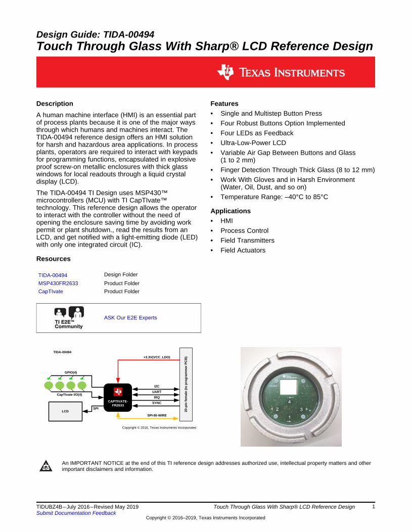
1.3 Block Diagram
Figure 1. TIDA-00494 Block Diagram
1.4 Highlighted ProductsThe key part of the TIDA-00494 system design is the MSP430FR2633 MCU, which allows capacitivesensing by pressing a button, even through the thick glass. Implementing CapTIvate technology enablesthe capacitive touch sensing capabilities of the MSP430FR2633 MCU. The MSP430FR2633 is able todrive LEDs and LCD thanks to its additional GPIOs and SPI and is powered and programmed through the20-pin female connector by the CAPTIVATE-PGMR Programmer PCB.
The MSP430FR2633 MCU communicates with a dedicated USB HID Bridge MCU located on theCAPTIVATE-PGMR PCB using UART or I2C communication to send sensor data and status to theCapTIvate Design Center as part of the sensor design and tuning process. A compact communicationsprotocol is provided as part of the CapTIvate™ software library along with UART and I2C drivers. Bothdrivers are located in the MSP430FR2633 ROM to minimize the impact on the FRAM memory footprint.
When used with CapTIvate protocol, the UART operates in a full-duplex mode using RX and TX pins, andthe I2C operates as an I2C slave using SDA and SCL pins with an additional pin P1.2/IRQ to generateinterrupt requests.
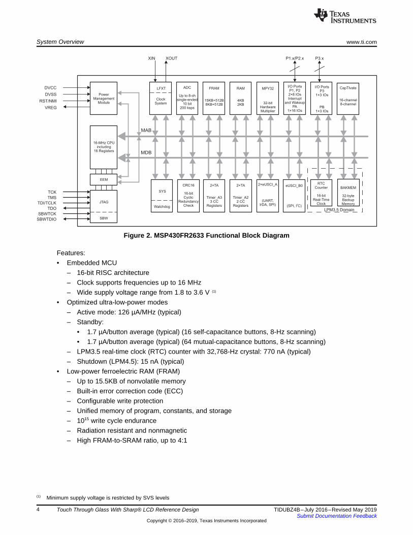
1.4.1 MSP430FR2633The MSP430FR2633 is a FRAM-based ultra-low-power MSP microcontroller that feature CapTIvate touchtechnology for buttons, sliders, wheels (BSW), and proximity applications. CapTIvate technology providesthe highest resolution capacitive-touch solution in the market with high reliability and noise immunity at thelowest power. CapTIvate technology supports concurrent self-capacitance and mutual-capacitanceelectrodes on the same design for maximum flexibility. Using the CapTIvate Design Center, engineers canquickly develop BSW applications with an easy-to-use GUI.
The TI MSP family of low-power MCUs consists of several devices that feature different sets ofperipherals targeted for various applications. The architecture, combined with extensive low-power modes,is optimized to achieve extended battery life in portable measurement applications. The MCU features apowerful 16-bit RISC CPU, 16-bit registers, and constant generators that contribute to maximum codeefficiency. The digitally controlled oscillator (DCO) allows the MCU to wake up from low-power modes toactive mode typically in less than 10 µs.
DVCC
RST/NMI
XIN XOUT P3.xP1.x/P2.x
DVSS
I/O PortsP1, P22×8 IOsInterrupt
and WakeupPA
1×16 IOs
ADC
Up to 8-chsingle-ended
10 bit200 ksps
ClockSystem
LFXT FRAM
15KB+512B8KB+512B
RAM
4KB2KB
Watchdog
SYS
CRC16
16-bitCyclic
RedundancyCheck
CapTIvate
16-channel8-channel
JTAG
SBW
I/O PortsP3
1×3 IOs
PB1×3 IOs
2×TA
Timer_A33 CC
Registers
EEM
MAB
MDB
16-MHz CPUincluding
16 Registers
PowerManagement
Module
MPY32
32-bitHardwareMultiplier
2×eUSCI_A
(UART,IrDA, SPI)
eUSCI_B0
(SPI, I C)2
RTCCounter
16-bitReal-Time
Clock
2×TA
Timer_A22 CC
Registers
VREG
BAKMEM
32-byteBackupMemory
LPM3.5 Domain
SBWTDIO
SBWTCK
TDO
TDI/TCLK
TMS
TCK
System Overview www.ti.com
4 TIDUBZ4B–July 2016–Revised May 2019Submit Documentation Feedback
Copyright © 2016–2019, Texas Instruments Incorporated
Touch Through Glass With Sharp® LCD Reference Design
(1) Minimum supply voltage is restricted by SVS levels
Figure 2. MSP430FR2633 Functional Block Diagram
Features:• Embedded MCU
– 16-bit RISC architecture– Clock supports frequencies up to 16 MHz– Wide supply voltage range from 1.8 to 3.6 V (1)
• Optimized ultra-low-power modes– Active mode: 126 µA/MHz (typical)– Standby:
• 1.7 µA/button average (typical) (16 self-capacitance buttons, 8-Hz scanning)• 1.7 µA/button average (typical) (64 mutual-capacitance buttons, 8-Hz scanning)
– LPM3.5 real-time clock (RTC) counter with 32,768-Hz crystal: 770 nA (typical)– Shutdown (LPM4.5): 15 nA (typical)
• Low-power ferroelectric RAM (FRAM)– Up to 15.5KB of nonvolatile memory– Built-in error correction code (ECC)– Configurable write protection– Unified memory of program, constants, and storage– 1015 write cycle endurance– Radiation resistant and nonmagnetic– High FRAM-to-SRAM ratio, up to 4:1
www.ti.com System Overview
5TIDUBZ4B–July 2016–Revised May 2019Submit Documentation Feedback
Copyright © 2016–2019, Texas Instruments Incorporated
Touch Through Glass With Sharp® LCD Reference Design
• Intelligent digital peripherals– Four 16-bit timers
• Two timers with three capture/compare registers each (Timer_A3)• Two timers with two capture/compare registers each (Timer_A2)
– One 16-bit timer associated with CapTIvate technology– One 16-bit counter-only RTC– 16-bit cyclic redundancy check (CRC)
• Enhanced serial communications– Two enhanced universal serial communication interfaces (eUSCI_A) support UART, IrDA, and SPI– One eUSCI (eUSCI_B) supports SPI and I2C
• High-performance analog– 8-channel 10-bit analog-to-digital converter (ADC)
• Internal 1.5-V reference• Sample-and-hold 200 ksps
– CapTIvate Technology—Capacitive touch• Performance
• Fast electrode scanning with four simultaneous scans• Support for high-resolution sliders with > 1024 points• 30-cm proximity sensing
• Reliability• Increased immunity to power line, RF, and other environmental noise• Built-in spread spectrum, automatic tuning, noise filtering, and debouncing algorithms• Enables Reliable Touch Solutions with 10-VRMS common-mode noise, 4-kV electrical fast
transients, and 15-kV electrostatic discharge, allowing for IEC‑61000-4-6, IEC-61000-4-4,and IEC‑61000-4-2 compliance
• Reduced RF emissions to simplify electrical designs• Support for metal touch and water rejection designs
• Flexibility• Up to 16 self-capacitance and 64 mutual-capacitance electrodes• Mix and match self- and mutual-capacitive electrodes in the same design• Supports multi-touch functionality• Wide range of capacitance detection, wide electrode range of 0 to 300 pF
• Low power• <0.9 µA/button in wake-on-touch mode, where capacitive measurement and touch detection
is done by hardware state machine while CPU is asleep• Wake-on-touch state machine allows electrode scanning while CPU is asleep• Hardware acceleration for environmental compensation, filtering, and threshold detection
• Ease of use• CapTIvate Design Center, PC GUI lets engineers design and tune capacitive buttons in real
time without having to write code• CapTIvate software library in ROM provides ample FRAM for customer application
System Overview www.ti.com
6 TIDUBZ4B–July 2016–Revised May 2019Submit Documentation Feedback
Copyright © 2016–2019, Texas Instruments Incorporated
Touch Through Glass With Sharp® LCD Reference Design
• Clock system (CS)– On-chip 32-kHz RC oscillator (REFO)– On-chip 16-MHz digitally controlled oscillator (DCO) with frequency-locked loop (FLL)
• ±1% accuracy with on-chip reference at room temperature– On-chip very low-frequency 10-kHz oscillator (VLO)– On-chip high-frequency modulation oscillator (MODOSC)– External 32-kHz crystal oscillator (LFXT)– Programmable MCLK prescalar of 1 to 128– SMCLK derived from MCLK with programmable prescalar of 1, 2, 4, or 8
• General input/output and pin functionality– Total of 19 I/Os on TSSOP-32 package– 16 interrupt pins (P1 and P2) can wake MCU from low-power modes
• Development tools and software– Ease-of-use ecosystem
• CapTIvate design center—code generation, customizable GUI, real-time tuning– Free professional development environments
• 12-KB ROM library includes CapTIvate touch libraries and driver libraries• Package options
– 32-pin: VQFN (RHB)– 32-pin: TSSOP (DA)– 24-pin: VQFN (RGE)– 24-pin: DSBGA (YQW)
For a complete module description, see the MSP430FR4xx and MSP430FR2xx Family User's Guide(SLAU445).
www.ti.com System Design Theory
7TIDUBZ4B–July 2016–Revised May 2019Submit Documentation Feedback
Copyright © 2016–2019, Texas Instruments Incorporated
Touch Through Glass With Sharp® LCD Reference Design
2 System Design TheoryThe TIDA-00494 is designed to fit in an explosive-proof enclosure as the one showed in Section 2.2. ThePCB has four buttons displaced according to certain rules (see Section 2.4), four LEDs, and one display(see Section 2.3) to indicate the buttons status. Everything is controlled by the MSP430FR2633 that canbe programmed and debugged by the CAPTIVATE-PGMR PCB, found in the MSP CapTIvate MCUDevelopment Kit, which is needed as well to collect data and display them on the MSP CapTIvate DesignCenter GUI.
Once the MSP430FR2633 is programmed, the board could be used even without CAPTIVATE-PGMRPCB and be powered externally (see Section 3).
2.1 Mechanical DesignDesigning the TIDA-00494 requires attention to a few key mechanical details. Note that the board is to behoused in a screw-on metallic enclosure (see Section 2.2), which can be removed by unscrewing the topunit. In order to prevent any interference with the electronics when the user removes the enclosure, theelectrodes board must not be in direct contact with the glass window. The distance between the windowglass and the electrode board can vary depending on the application.
TI recommends keeping the TIDA-00494 as close as possible to the glass window for better performance(See Section 2.4 and Section 4.2).
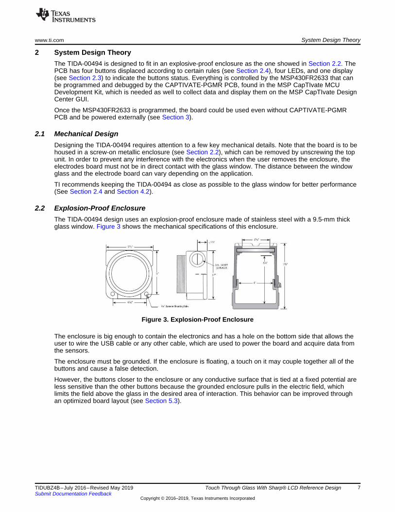
2.2 Explosion-Proof EnclosureThe TIDA-00494 design uses an explosion-proof enclosure made of stainless steel with a 9.5-mm thickglass window. Figure 3 shows the mechanical specifications of this enclosure.
Figure 3. Explosion-Proof Enclosure
The enclosure is big enough to contain the electronics and has a hole on the bottom side that allows theuser to wire the USB cable or any other cable, which are used to power the board and acquire data fromthe sensors.
The enclosure must be grounded. If the enclosure is floating, a touch on it may couple together all of thebuttons and cause a false detection.
However, the buttons closer to the enclosure or any conductive surface that is tied at a fixed potential areless sensitive than the other buttons because the grounded enclosure pulls in the electric field, whichlimits the field above the glass in the desired area of interaction. This behavior can be improved throughan optimized board layout (see Section 5.3).
System Design Theory www.ti.com
8 TIDUBZ4B–July 2016–Revised May 2019Submit Documentation Feedback
Copyright © 2016–2019, Texas Instruments Incorporated
Touch Through Glass With Sharp® LCD Reference Design
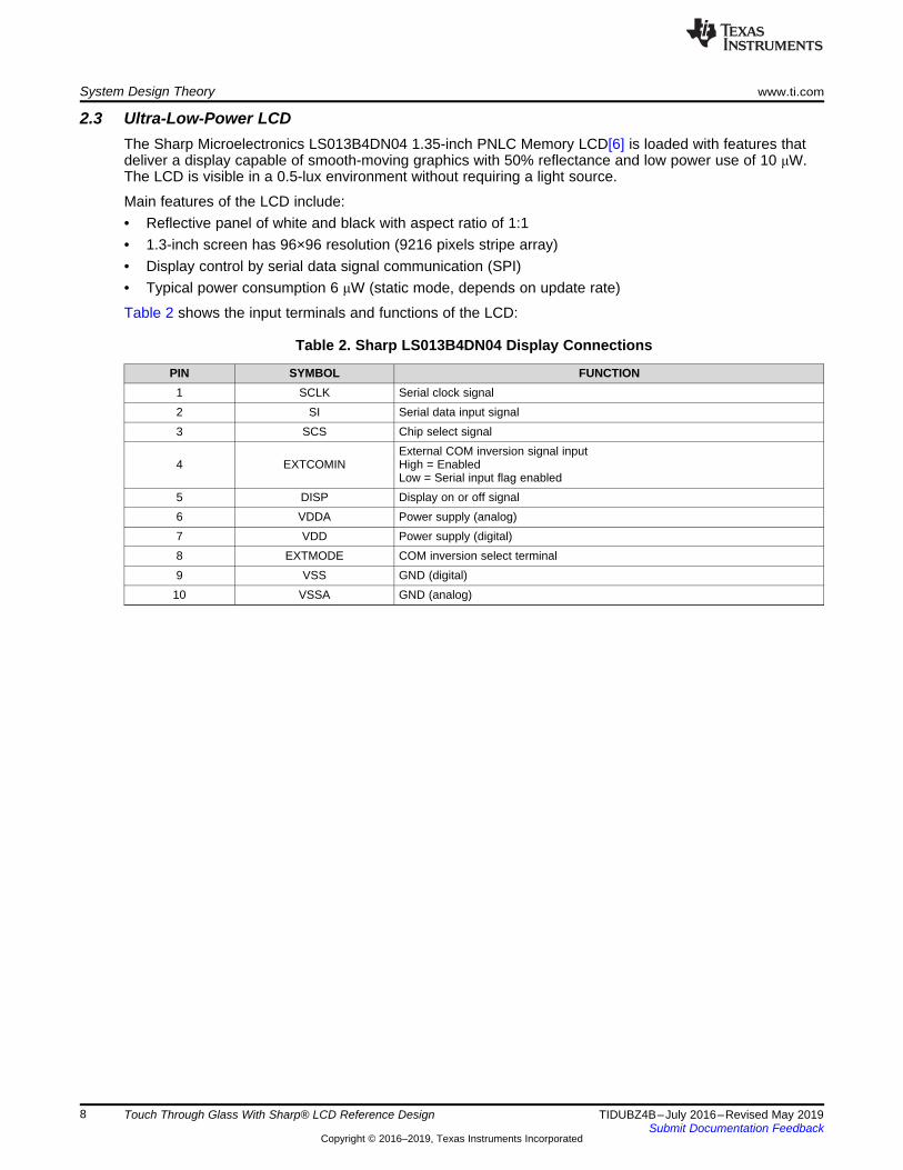
2.3 Ultra-Low-Power LCDThe Sharp Microelectronics LS013B4DN04 1.35-inch PNLC Memory LCD[6] is loaded with features thatdeliver a display capable of smooth-moving graphics with 50% reflectance and low power use of 10 μW.The LCD is visible in a 0.5-lux environment without requiring a light source.
Main features of the LCD include:• Reflective panel of white and black with aspect ratio of 1:1• 1.3-inch screen has 96×96 resolution (9216 pixels stripe array)• Display control by serial data signal communication (SPI)• Typical power consumption 6 μW (static mode, depends on update rate)
Table 2 shows the input terminals and functions of the LCD:
Table 2. Sharp LS013B4DN04 Display Connections
PIN SYMBOL FUNCTION1 SCLK Serial clock signal2 SI Serial data input signal3 SCS Chip select signal
4 EXTCOMINExternal COM inversion signal inputHigh = EnabledLow = Serial input flag enabled
5 DISP Display on or off signal6 VDDA Power supply (analog)7 VDD Power supply (digital)8 EXTMODE COM inversion select terminal9 VSS GND (digital)
10 VSSA GND (analog)
Glass
Air gap
Button
FR-4 corelaminate
Copper
Copyright © 2016, Texas Instruments Incorporated
A
Conductive plates
Dielectric
d
r 0
AC
d= Î ´ Î ´
www.ti.com System Design Theory
9TIDUBZ4B–July 2016–Revised May 2019Submit Documentation Feedback
Copyright © 2016–2019, Texas Instruments Incorporated
Touch Through Glass With Sharp® LCD Reference Design
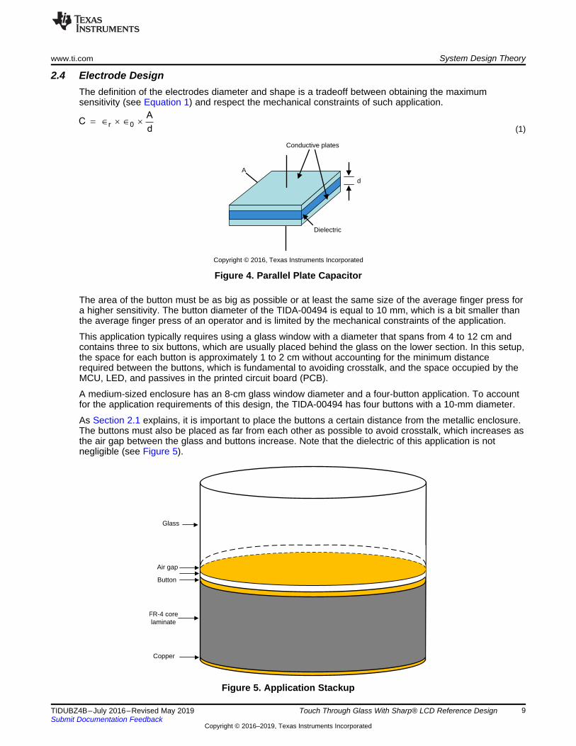
2.4 Electrode DesignThe definition of the electrodes diameter and shape is a tradeoff between obtaining the maximumsensitivity (see Equation 1) and respect the mechanical constraints of such application.
(1)
Figure 4. Parallel Plate Capacitor
The area of the button must be as big as possible or at least the same size of the average finger press fora higher sensitivity. The button diameter of the TIDA-00494 is equal to 10 mm, which is a bit smaller thanthe average finger press of an operator and is limited by the mechanical constraints of the application.
This application typically requires using a glass window with a diameter that spans from 4 to 12 cm andcontains three to six buttons, which are usually placed behind the glass on the lower section. In this setup,the space for each button is approximately 1 to 2 cm without accounting for the minimum distancerequired between the buttons, which is fundamental to avoiding crosstalk, and the space occupied by theMCU, LED, and passives in the printed circuit board (PCB).
A medium-sized enclosure has an 8-cm glass window diameter and a four-button application. To accountfor the application requirements of this design, the TIDA-00494 has four buttons with a 10-mm diameter.
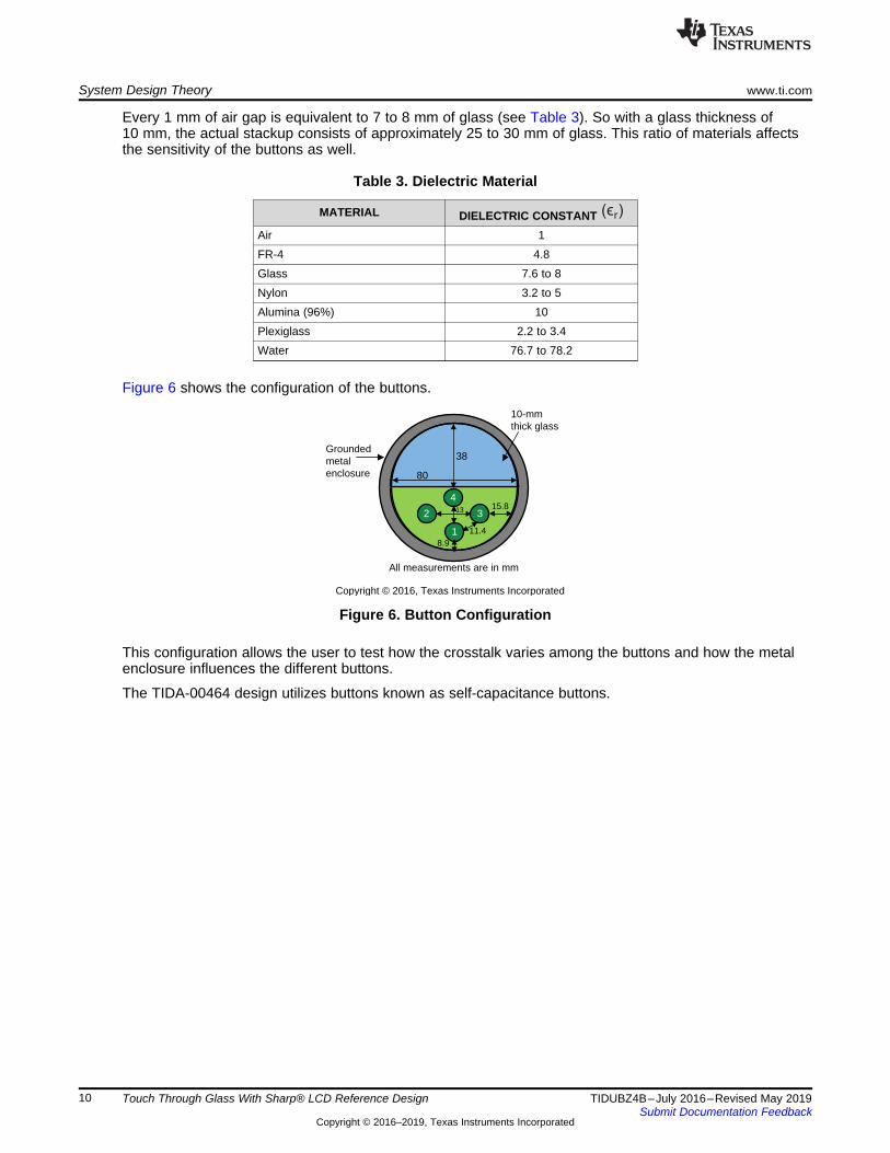
As Section 2.1 explains, it is important to place the buttons a certain distance from the metallic enclosure.The buttons must also be placed as far from each other as possible to avoid crosstalk, which increases asthe air gap between the glass and buttons increase. Note that the dielectric of this application is notnegligible (see Figure 5).
Figure 5. Application Stackup
Copyright © 2016, Texas Instruments Incorporated
Groundedmetalenclosure
10-mmthick glass
38
80
1
2
4
3
All measurements are in mm
15.8
11.48.9
13
(! )r
System Design Theory www.ti.com
10 TIDUBZ4B–July 2016–Revised May 2019Submit Documentation Feedback
Copyright © 2016–2019, Texas Instruments Incorporated
Touch Through Glass With Sharp® LCD Reference Design
Every 1 mm of air gap is equivalent to 7 to 8 mm of glass (see Table 3). So with a glass thickness of10 mm, the actual stackup consists of approximately 25 to 30 mm of glass. This ratio of materials affectsthe sensitivity of the buttons as well.
Table 3. Dielectric Material
MATERIAL DIELECTRIC CONSTANTAir 1FR-4 4.8Glass 7.6 to 8Nylon 3.2 to 5Alumina (96%) 10Plexiglass 2.2 to 3.4Water 76.7 to 78.2
Figure 6 shows the configuration of the buttons.
Figure 6. Button Configuration
This configuration allows the user to test how the crosstalk varies among the buttons and how the metalenclosure influences the different buttons.
The TIDA-00464 design utilizes buttons known as self-capacitance buttons.
RX RX
PCBTX/RX
Front panel
www.ti.com System Design Theory
11TIDUBZ4B–July 2016–Revised May 2019Submit Documentation Feedback
Copyright © 2016–2019, Texas Instruments Incorporated
Touch Through Glass With Sharp® LCD Reference Design
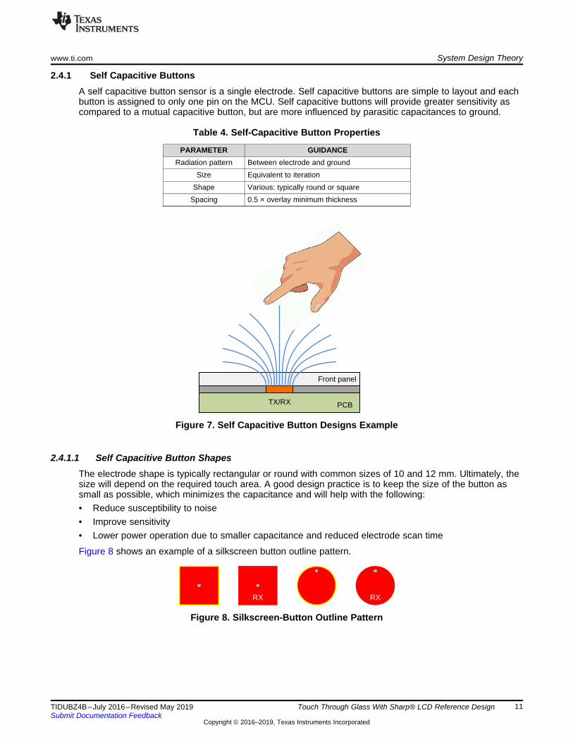
2.4.1 Self Capacitive ButtonsA self capacitive button sensor is a single electrode. Self capacitive buttons are simple to layout and eachbutton is assigned to only one pin on the MCU. Self capacitive buttons will provide greater sensitivity ascompared to a mutual capacitive button, but are more influenced by parasitic capacitances to ground.
Table 4. Self-Capacitive Button Properties
PARAMETER GUIDANCERadiation pattern Between electrode and ground
Size Equivalent to iterationShape Various: typically round or square
Spacing 0.5 × overlay minimum thickness
Figure 7. Self Capacitive Button Designs Example
2.4.1.1 Self Capacitive Button ShapesThe electrode shape is typically rectangular or round with common sizes of 10 and 12 mm. Ultimately, thesize will depend on the required touch area. A good design practice is to keep the size of the button assmall as possible, which minimizes the capacitance and will help with the following:• Reduce susceptibility to noise• Improve sensitivity• Lower power operation due to smaller capacitance and reduced electrode scan time
Figure 8 shows an example of a silkscreen button outline pattern.
Figure 8. Silkscreen-Button Outline Pattern
Finger sizes
10 mm
5 mm
Effective area for larger finger
ElectrodeDecal
Larger finger size
Electrode
Decal
Overlay
PCB
Ground pour
15 mm 6 mm
Effective area for smaller finger
ElectrodeDecal
Smaller finger size
Finger sizes
10 mm
5 mm
Effective area for larger finger
ElectrodeDecal
Larger finger size
Electrode
Decal
Overlay
PCB
Ground pour
20 mm 14 mm
Effective area for smaller finger
ElectrodeDecal
Smaller finger size
System Design Theory www.ti.com
12 TIDUBZ4B–July 2016–Revised May 2019Submit Documentation Feedback
Copyright © 2016–2019, Texas Instruments Incorporated
Touch Through Glass With Sharp® LCD Reference Design
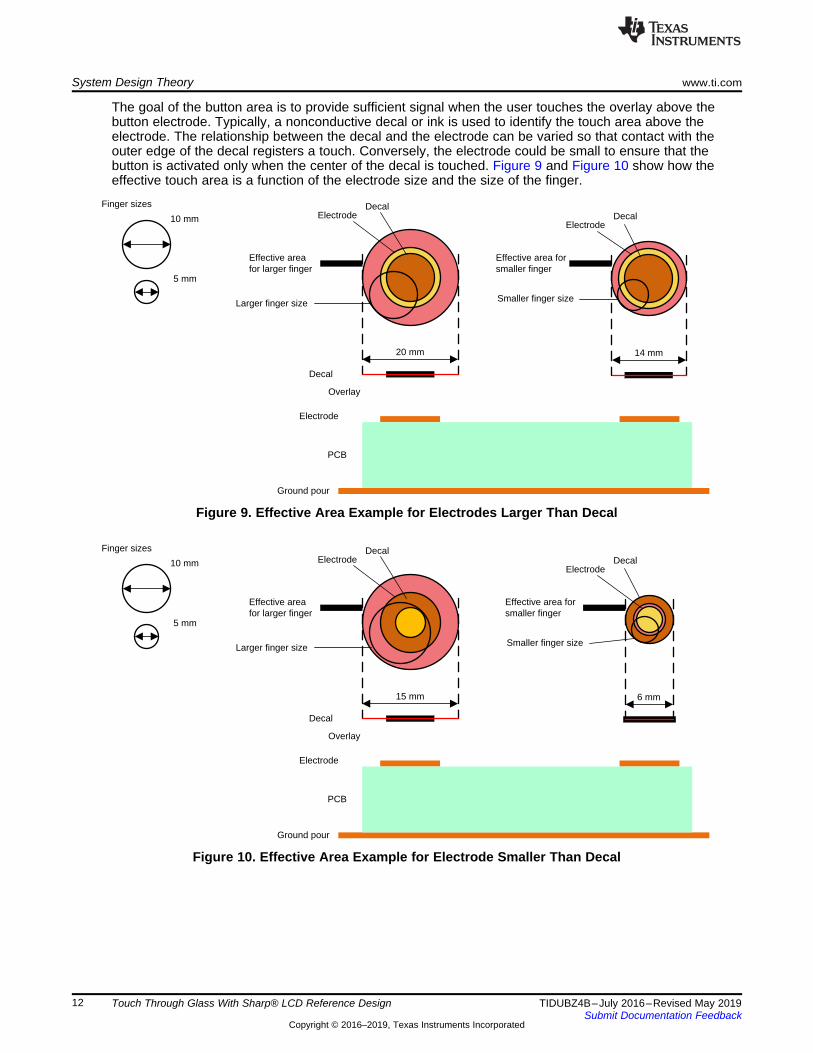
The goal of the button area is to provide sufficient signal when the user touches the overlay above thebutton electrode. Typically, a nonconductive decal or ink is used to identify the touch area above theelectrode. The relationship between the decal and the electrode can be varied so that contact with theouter edge of the decal registers a touch. Conversely, the electrode could be small to ensure that thebutton is activated only when the center of the decal is touched. Figure 9 and Figure 10 show how theeffective touch area is a function of the electrode size and the size of the finger.
Figure 9. Effective Area Example for Electrodes Larger Than Decal
Figure 10. Effective Area Example for Electrode Smaller Than Decal
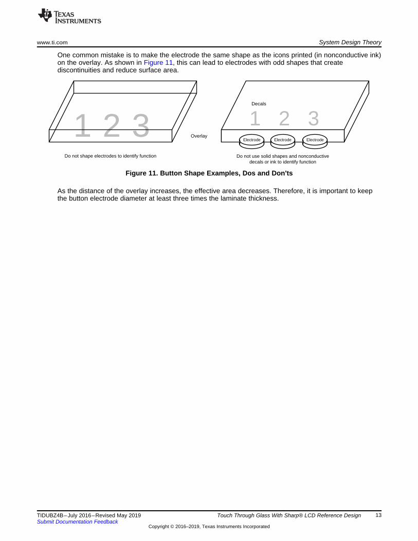
1 2 3 1 2 3
Do not shape electrodes to identify function Do not use solid shapes and nonconductive decals or ink to identify function
OverlayElectrode Electrode Electrode
Decals
www.ti.com System Design Theory
13TIDUBZ4B–July 2016–Revised May 2019Submit Documentation Feedback
Copyright © 2016–2019, Texas Instruments Incorporated
Touch Through Glass With Sharp® LCD Reference Design
One common mistake is to make the electrode the same shape as the icons printed (in nonconductive ink)on the overlay. As shown in Figure 11, this can lead to electrodes with odd shapes that creatediscontinuities and reduce surface area.
Figure 11. Button Shape Examples, Dos and Don'ts
As the distance of the overlay increases, the effective area decreases. Therefore, it is important to keepthe button electrode diameter at least three times the laminate thickness.
Getting Started Hardware and Firmware www.ti.com
14 TIDUBZ4B–July 2016–Revised May 2019Submit Documentation Feedback
Copyright © 2016–2019, Texas Instruments Incorporated
Touch Through Glass With Sharp® LCD Reference Design
3 Getting Started Hardware and Firmware
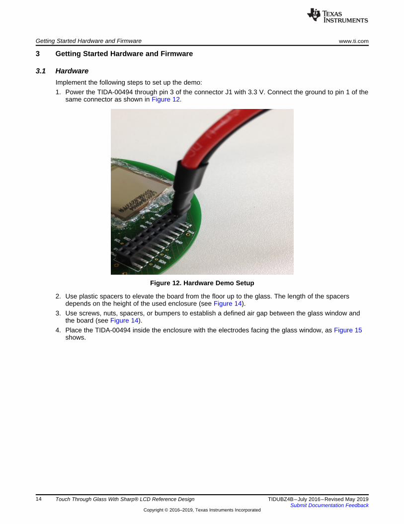
3.1 HardwareImplement the following steps to set up the demo:1. Power the TIDA-00494 through pin 3 of the connector J1 with 3.3 V. Connect the ground to pin 1 of the
same connector as shown in Figure 12.
Figure 12. Hardware Demo Setup
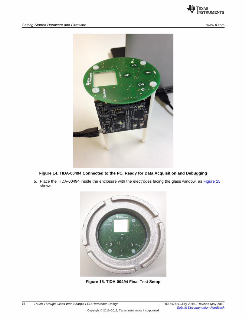
2. Use plastic spacers to elevate the board from the floor up to the glass. The length of the spacersdepends on the height of the used enclosure (see Figure 14).
3. Use screws, nuts, spacers, or bumpers to establish a defined air gap between the glass window andthe board (see Figure 14).
4. Place the TIDA-00494 inside the enclosure with the electrodes facing the glass window, as Figure 15shows.
www.ti.com Getting Started Hardware and Firmware
15TIDUBZ4B–July 2016–Revised May 2019Submit Documentation Feedback
Copyright © 2016–2019, Texas Instruments Incorporated
Touch Through Glass With Sharp® LCD Reference Design
For data acquisition and debug services, the CAPTIVATE-PGMR programmer PCB available with theCapTIvate Design Kit is needed.
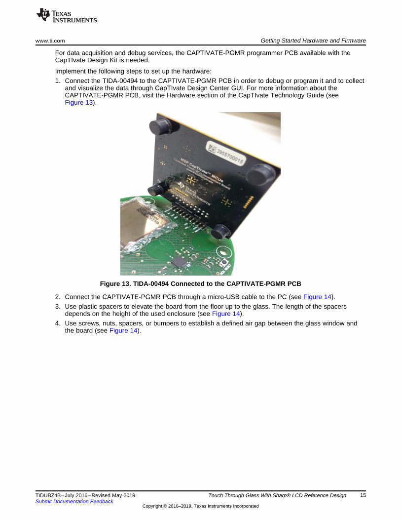
Implement the following steps to set up the hardware:1. Connect the TIDA-00494 to the CAPTIVATE-PGMR PCB in order to debug or program it and to collect
and visualize the data through CapTIvate Design Center GUI. For more information about theCAPTIVATE-PGMR PCB, visit the Hardware section of the CapTIvate Technology Guide (seeFigure 13).
Figure 13. TIDA-00494 Connected to the CAPTIVATE-PGMR PCB
2. Connect the CAPTIVATE-PGMR PCB through a micro-USB cable to the PC (see Figure 14).3. Use plastic spacers to elevate the board from the floor up to the glass. The length of the spacers
depends on the height of the used enclosure (see Figure 14).4. Use screws, nuts, spacers, or bumpers to establish a defined air gap between the glass window and
the board (see Figure 14).
Getting Started Hardware and Firmware www.ti.com
16 TIDUBZ4B–July 2016–Revised May 2019Submit Documentation Feedback
Copyright © 2016–2019, Texas Instruments Incorporated
Touch Through Glass With Sharp® LCD Reference Design
Figure 14. TIDA-00494 Connected to the PC, Ready for Data Acquisition and Debugging
5. Place the TIDA-00494 inside the enclosure with the electrodes facing the glass window, as Figure 15shows.
Figure 15. TIDA-00494 Final Test Setup
www.ti.com Getting Started Hardware and Firmware
17TIDUBZ4B–July 2016–Revised May 2019Submit Documentation Feedback
Copyright © 2016–2019, Texas Instruments Incorporated
Touch Through Glass With Sharp® LCD Reference Design
3.2 FirmwareTo download the software files for this reference design, please see the link athttp://www.ti.com/tool/TIDA-00494.
The TIDA-00494 ships pre-programmed with demo software where each buttons press corresponds to alight-up LED and a confirmation string in the display.
For data acquisition and debug services, the CAPTIVATE-PGMR programmer PCB available with theCapTIvate Design Kit is needed.
Once the CAPTIVATE-PGMR programmer PCB is connected to the TIDA-00494 and to the PC (seeSection 3), it is possible through Code Composer Studio™ (CCS) and the CapTIvate Design Center GUIto acquire data, debug the software, and modify it according to the needs of your application. To installCCS and the CapTIvate Design Center GUI and learn how to use them, look at the "Getting Started withthe MCU Development Kit" section of the CapTIvate Technology Guide.
[ ]Sample size
B1n 0
AVG,B1
Untouched nUntouched
Sample size
==å
[ ]Sample size
B1n 0
AVG,B1
Touched nTouched
Sample size
==å
Copyright © 2016, Texas Instruments Incorporated
UntouchAVG, B1 TouchAVG, B1TS
1Untouch, B1 1Touch, B1
±31Touch, B1 +31Untouch,B1
Testing and Results www.ti.com
18 TIDUBZ4B–July 2016–Revised May 2019Submit Documentation Feedback
Copyright © 2016–2019, Texas Instruments Incorporated
Touch Through Glass With Sharp® LCD Reference Design
4 Testing and Results
4.1 Test SetupThe TIDA-00494 and the CAPTIVATE-PGMR PCB must be connected as outlined in Section 3 and thencontained in the explosive-proof enclosure. A USB wire is the only object that is allowed to protrude fromthe enclosure and this USB must be connected to a laptop, which uses the CapTIvate Design Center GUIto acquire the sensor data.
Adjusting the conversion gain and the conversion count is an important step that the user can control inthe CapTIvate Design Center. Adjust these properties by opening the ButtonGroupSensor properties witha double-click on the button group icon and then navigating to the Conversion_Control tab.
The conversion gain and conversion count are the fundamental parameters used to establish theperformance of the sensor. These parameters determine the resolution, sensitivity, and requiredconversion time.
The TIDA-00494 design has a conversion gain count equal to 1400 and a conversion gain equal to 200.Increasing the strength of the infinite impulse response (IIR) filter to improve the signal-to-noise ratio(SNR) is also possible. This property is controlled by the Count Filter Beta parameter located in the Tuningtab for each sensor.
The TIDA-00494 design has a count filter beta set to 3.
The following tests were performed:• Touch• Touch with gloves• False touch
In each test, 1000 samples were taken while pressing a button, and 1000 samples were taken withoutperforming any action. The sampling was followed by calculating the SNR and crosstalk among thebuttons.
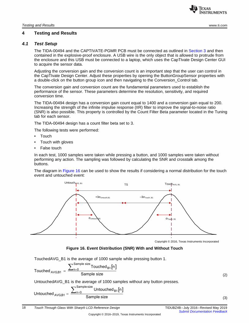
The diagram in Figure 16 can be used to show the results if considering a normal distribution for the touchevent and untouched event:
Figure 16. Event Distribution (SNR) With and Without Touch
TouchedAVG_B1 is the average of 1000 sample while pressing button 1.
(2)
UntouchedAVG_B1 is the average of 1000 samples without any button presses.
(3)

( )Untouch,B1 Touch,B1
TSSNR dB 20 log 9.5 dB
æ ö= ´ >ç ÷
ç ÷s + sè ø
( ) AVG,B1 AVG,B1Touch strength TS Untouched Touched= -
( ) AVG,B1 AVG,B1
AVG,B1 AVG,B1 Untouch,B1 Touch,B1Untouch,B1 Touch,B1
T UT U 3 3
-- > s +s Þ >
s +s
[ ]( )Sample size 2
B1 AVG,B1n 0
Untouch,B1
Untouched n Untouched
Sample size
=
æ ö-ç ÷s = ç ÷
ç ÷è ø
å
[ ]( )Sample size 2
B1 AVG,B1n 0
Touch,B1
Touched n Touched
Sample size
=
æ ö-ç ÷s = ç ÷
ç ÷è ø
å
AVG,B1 Touch,B1 AVG,B1 Untouch,B1T 3 U 3- s > + s
www.ti.com Testing and Results
19TIDUBZ4B–July 2016–Revised May 2019Submit Documentation Feedback
Copyright © 2016–2019, Texas Instruments Incorporated
Touch Through Glass With Sharp® LCD Reference Design
Table 5 shows the SNR and the probability of a false event as a function of the number of σ.
Table 5. SNR and Probability of False Event inFunction of Number of σ
zσ SNR (dB) PROBABILITY OFFALSE EVENT
1σ 0 31.73%2σ 6 4.55%3σ 9.5 0.27%4σ 12 60 ppm5σ 14 0.57 ppm
To achieve a 0.27% probability of a false event, ensure that TouchedAVG,B1 minus 3σTOUCH,B1 is bigger thanUntouchedAVG,B1 plus 3σUntouch,B1:
(4)
where
(5)
(6)
The calculations from Equation 4 can be further simplified in Equation 7:
(7)
Define the touch strength (TS) in Equation 8 using the previous calculations from Equation 7:
(8)
Calculate the SNR in dB in Equation 7:
(9)
To ensure that the probability of a button being touched is equal to 99.73%, the SNR must be greater than9.5 dB (see Table 5).
( )B1,B2Untouch,B2 Touch,B1
TSCrosstalk dB 20 log 9.5 dB
æ ö= ´ >ç ÷
ç ÷s + sè ø
Copyright © 2016, Texas Instruments Incorporated
UntouchAVG, B2 TouchAVG, B1TS
1Untouch, B2 1Touch, B1
±31Touch, B1 +31Untouch,B2
Testing and Results www.ti.com
20 TIDUBZ4B–July 2016–Revised May 2019Submit Documentation Feedback
Copyright © 2016–2019, Texas Instruments Incorporated
Touch Through Glass With Sharp® LCD Reference Design
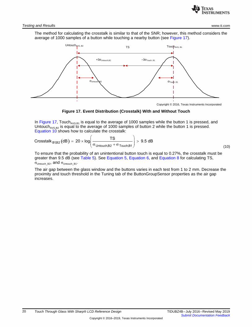
The method for calculating the crosstalk is similar to that of the SNR; however, this method considers theaverage of 1000 samples of a button while touching a nearby button (see Figure 17).
Figure 17. Event Distribution (Crosstalk) With and Without Touch
In Figure 17, TouchAVG,B1 is equal to the average of 1000 samples while the button 1 is pressed, andUntouchAVG,B2 is equal to the average of 1000 samples of button 2 while the button 1 is pressed.Equation 10 shows how to calculate the crosstalk:
(10)
To ensure that the probability of an unintentional button touch is equal to 0.27%, the crosstalk must begreater than 9.5 dB (see Table 5). See Equation 5, Equation 6, and Equation 8 for calculating TS,σUntouch_B2, and σUntouch_B1.
The air gap between the glass window and the buttons varies in each test from 1 to 2 mm. Decrease theproximity and touch threshold in the Tuning tab of the ButtonGroupSensor properties as the air gapincreases.
www.ti.com Testing and Results
21TIDUBZ4B–July 2016–Revised May 2019Submit Documentation Feedback
Copyright © 2016–2019, Texas Instruments Incorporated
Touch Through Glass With Sharp® LCD Reference Design
4.2 Test Data
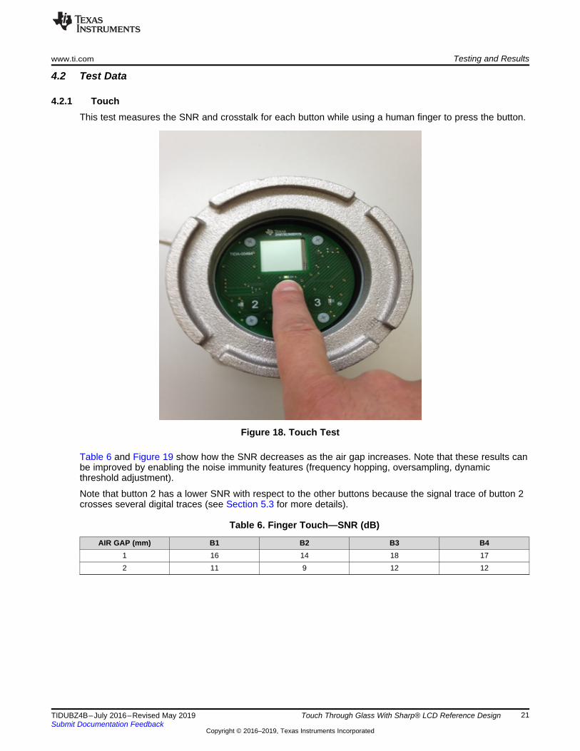
4.2.1 TouchThis test measures the SNR and crosstalk for each button while using a human finger to press the button.
Figure 18. Touch Test
Table 6 and Figure 19 show how the SNR decreases as the air gap increases. Note that these results canbe improved by enabling the noise immunity features (frequency hopping, oversampling, dynamicthreshold adjustment).
Note that button 2 has a lower SNR with respect to the other buttons because the signal trace of button 2crosses several digital traces (see Section 5.3 for more details).
Table 6. Finger Touch—SNR (dB)
AIR GAP (mm) B1 B2 B3 B41 16 14 18 172 11 9 12 12
AirGap (mm)
Cro
ssT
alk
(dB
)
1 1.2 1.4 1.6 1.8 20
5
10
15
20
25
30
35
40
D002
B1vsB2B1vsB3B1vsB4B2vsB1B2vsB3B2vsB4B3vsB1B3vsB2B3vsB4B4vsB1B4vsB2B4vsB3
AirGap (mm)
SN
R (
dB)
1 1.2 1.4 1.6 1.8 20
2
4
6
8
10
12
14
16
18
20
D001
B1B2B3B4
Testing and Results www.ti.com
22 TIDUBZ4B–July 2016–Revised May 2019Submit Documentation Feedback
Copyright © 2016–2019, Texas Instruments Incorporated
Touch Through Glass With Sharp® LCD Reference Design
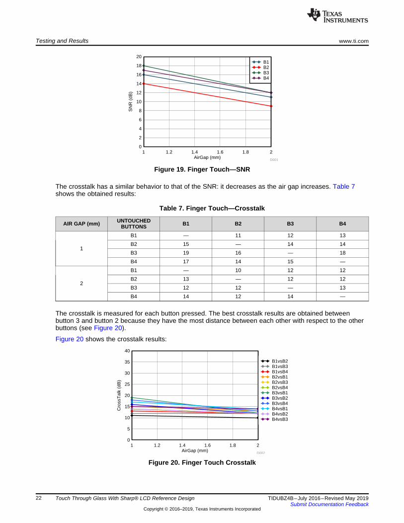
Figure 19. Finger Touch—SNR
The crosstalk has a similar behavior to that of the SNR: it decreases as the air gap increases. Table 7shows the obtained results:
Table 7. Finger Touch—Crosstalk
AIR GAP (mm) UNTOUCHEDBUTTONS B1 B2 B3 B4
1
B1 — 11 12 13B2 15 — 14 14B3 19 16 — 18B4 17 14 15 —
2
B1 — 10 12 12B2 13 — 12 12B3 12 12 — 13B4 14 12 14 —
The crosstalk is measured for each button pressed. The best crosstalk results are obtained betweenbutton 3 and button 2 because they have the most distance between each other with respect to the otherbuttons (see Figure 20).
Figure 20 shows the crosstalk results:
Figure 20. Finger Touch Crosstalk
AirGap (mm)
SN
R (
dB)
1 1.2 1.4 1.6 1.8 20
5
10
15
20
25
30
D003
B1B2B3B4
www.ti.com Testing and Results
23TIDUBZ4B–July 2016–Revised May 2019Submit Documentation Feedback
Copyright © 2016–2019, Texas Instruments Incorporated
Touch Through Glass With Sharp® LCD Reference Design
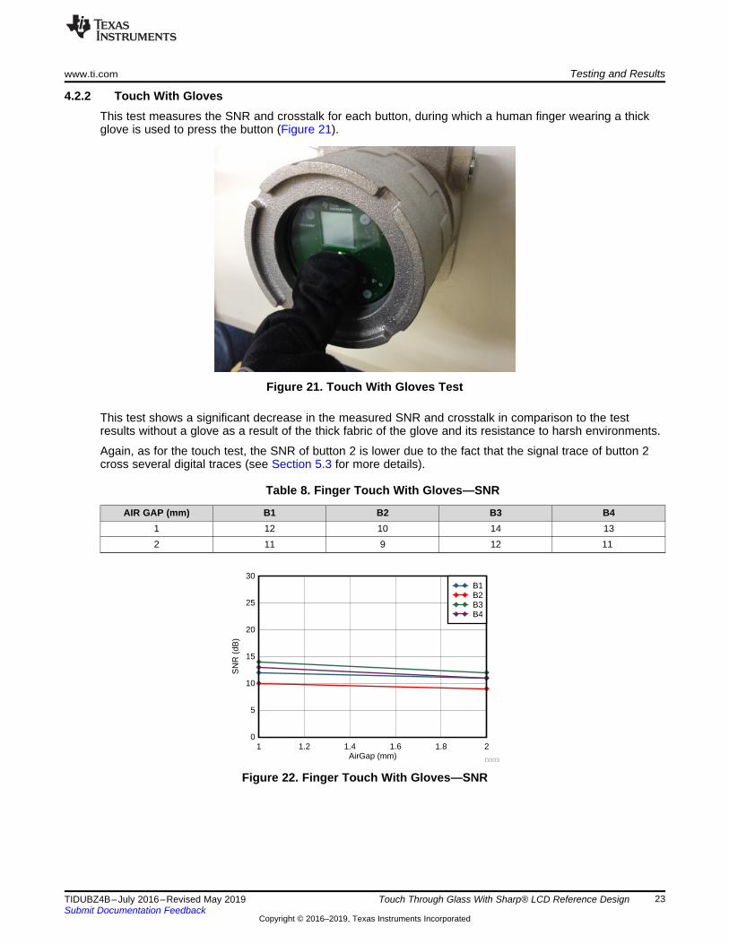
4.2.2 Touch With GlovesThis test measures the SNR and crosstalk for each button, during which a human finger wearing a thickglove is used to press the button (Figure 21).
Figure 21. Touch With Gloves Test
This test shows a significant decrease in the measured SNR and crosstalk in comparison to the testresults without a glove as a result of the thick fabric of the glove and its resistance to harsh environments.
Again, as for the touch test, the SNR of button 2 is lower due to the fact that the signal trace of button 2cross several digital traces (see Section 5.3 for more details).
Table 8. Finger Touch With Gloves—SNR
AIR GAP (mm) B1 B2 B3 B41 12 10 14 132 11 9 12 11
Figure 22. Finger Touch With Gloves—SNR
AirGap (mm)
Cro
ssT
alk
(dB
)
1 1.2 1.4 1.6 1.8 20
5
10
15
20
25
30
D004
B1vsB2B1vsB3B1vsB4B2vsB1B2vsB3B2vsB4B3vsB1B3vsB2B3vsB4B4vsB1B4vsB2B4vsB3
Testing and Results www.ti.com
24 TIDUBZ4B–July 2016–Revised May 2019Submit Documentation Feedback
Copyright © 2016–2019, Texas Instruments Incorporated
Touch Through Glass With Sharp® LCD Reference Design
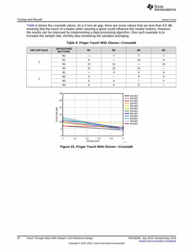
Table 9 shows the crosstalk values. At a 2-mm air gap, there are some values that are less than 9.5 dB,meaning that the touch of a button when wearing a glove could influence the nearby buttons. However,the results can be improved by implementing a data processing algorithm. One such example is toincrease the sample rate, thereby also increasing the samples averaging.
Table 9. Finger Touch With Gloves—Crosstalk
AIR GAP (mm) UNTOUCHEDBUTTONS B1 B2 B3 B4
1
B1 — 7 7 7B2 9 — 10 9B3 12 11 — 13B4 12 10 10 —
2
B1 — 4 6 6B2 5 — 9 6B3 5 6 — 5B4 4 4 5 —
Figure 23. Finger Touch With Gloves—Crosstalk
Copyright © 2016, Texas Instruments Incorporated
Groundedmetalenclosure
10-mmthick glass
38
80
1
2
4
3
All measurements are in mm
15.8
11.48.9
13
www.ti.com Testing and Results
25TIDUBZ4B–July 2016–Revised May 2019Submit Documentation Feedback
Copyright © 2016–2019, Texas Instruments Incorporated
Touch Through Glass With Sharp® LCD Reference Design
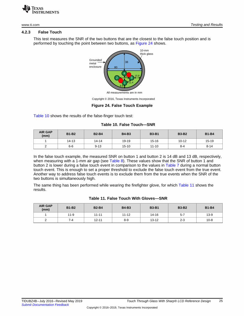
4.2.3 False TouchThis test measures the SNR of the two buttons that are the closest to the false touch position and isperformed by touching the point between two buttons, as Figure 24 shows.
Figure 24. False Touch Example
Table 10 shows the results of the false-finger touch test:
Table 10. False Touch—SNR
AIR GAP(mm) B1-B2 B2-B4 B4-B3 B3-B1 B3-B2 B1-B4
1 14-13 14-14 19-19 15-16 10-12 15-192 6-6 9-13 15-10 11-10 8-4 8-14
In the false touch example, the measured SNR on button 1 and button 2 is 14 dB and 13 dB, respectively,when measuring with a 1-mm air gap (see Table 8). These values show that the SNR of button 1 andbutton 2 is lower during a false touch event in comparison to the values in Table 7 during a normal buttontouch event. This is enough to set a proper threshold to exclude the false touch event from the true event.Another way to address false touch events is to exclude them from the true events when the SNR of thetwo buttons is simultaneously high.
The same thing has been performed while wearing the firefighter glove, for which Table 11 shows theresults.
Table 11. False Touch With Gloves—SNR
AIR GAP(mm) B1-B2 B2-B4 B4-B3 B3-B1 B3-B2 B1-B4
1 11-9 11-11 11-12 14-16 5-7 13-92 7-4 12-11 8-9 13-12 2-3 10-8
Testing and Results www.ti.com
26 TIDUBZ4B–July 2016–Revised May 2019Submit Documentation Feedback
Copyright © 2016–2019, Texas Instruments Incorporated
Touch Through Glass With Sharp® LCD Reference Design
4.3 CapTIvate Design Center SNR ToolThis section is an extension of the design that includes additional measurements and test results basedon the SNR tool available in CDC V 1_80_00_xx.
This section will give an explanation of the test results and recommendations to ensure functional stability.
4.3.1 Tools and Test DescriptionThe following tools were used for testing:• CDC V 1_80_00_xx & SNR• TIDA-0494 HW setup
– Modifications: removed the resistors and LEDs from the TOP layer– Enclosure GND connected with the board
• Spacers between the bottom of the glass and the PCB
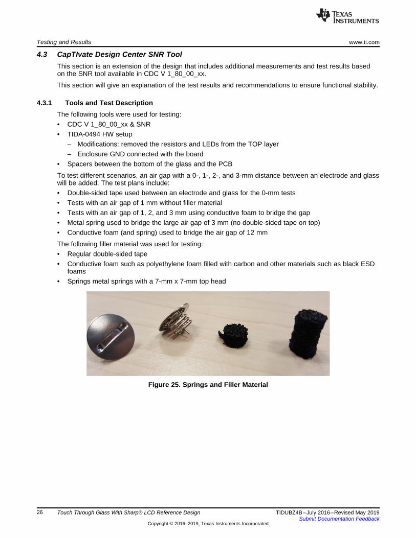
To test different scenarios, an air gap with a 0-, 1-, 2-, and 3-mm distance between an electrode and glasswill be added. The test plans include:• Double-sided tape used between an electrode and glass for the 0-mm tests• Tests with an air gap of 1 mm without filler material• Tests with an air gap of 1, 2, and 3 mm using conductive foam to bridge the gap• Metal spring used to bridge the large air gap of 3 mm (no double-sided tape on top)• Conductive foam (and spring) used to bridge the air gap of 12 mm
The following filler material was used for testing:• Regular double-sided tape• Conductive foam such as polyethylene foam filled with carbon and other materials such as black ESD
foams• Springs metal springs with a 7-mm x 7-mm top head
Figure 25. Springs and Filler Material
www.ti.com Testing and Results
27TIDUBZ4B–July 2016–Revised May 2019Submit Documentation Feedback
Copyright © 2016–2019, Texas Instruments Incorporated
Touch Through Glass With Sharp® LCD Reference Design
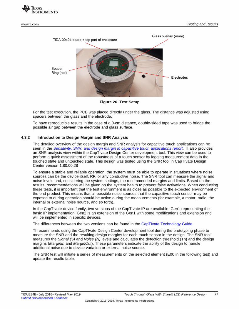
Figure 26. Test Setup
For the test execution, the PCB was placed directly under the glass. The distance was adjusted usingspacers between the glass and the electrode.
To have reproducible results in the case of a 0-cm distance, double-sided tape was used to bridge thepossible air gap between the electrode and glass surface.
4.3.2 Introduction to Design Margin and SNR AnalysisThe detailed overview of the design margin and SNR analysis for capacitive touch applications can beseen in the Sensitivity, SNR, and design margin in capacitive touch applications report. TI also providesan SNR analysis view within the CapTIvate Design Center development tool. This view can be used toperform a quick assessment of the robustness of a touch sensor by logging measurement data in thetouched state and untouched state. This design was tested using the SNR tool in CapTIvate DesignCenter version 1.80.00.28
To ensure a stable and reliable operation, the system must be able to operate in situations where noisesources can be the device itself, RF, or any conductive noise. The SNR tool can measure the signal andnoise levels and, considering the system settings, the recommended margins and limits. Based on theresults, recommendations will be given on the system health to prevent false activations. When conductingthese tests, it is important that the test environment is as close as possible to the expected environment ofthe end product. This means that all possible noise sources that the capacitive touch sensor may beexposed to during operation should be active during the measurements (for example, a motor, radio, theinternal or external noise source, and so forth).
In the CapTIvate device family, two versions of the CapTIvate IP are available. Gen1 representing thebasic IP implementation. Gen2 is an extension of the Gen1 with some modifications and extension andwill be implemented in specific devices.
The differences between the two versions can be found in the CapTIvate Technology Guide.
TI recommends using the CapTIvate Design Center development tool during the prototyping phase tomeasure the SNR and the resulting design margins for each touch sensor in the design. The SNR toolmeasures the Signal (S) and Noise (N) levels and calculates the detection threshold (Th) and the designmargins (MarginIn and MarginOut). These parameters indicate the ability of the design to handleadditional noise due to device variation or external noise source.
The SNR test will initiate a series of measurements on the selected element (E00 in the following test) andupdate the results table.
Testing and Results www.ti.com
28 TIDUBZ4B–July 2016–Revised May 2019Submit Documentation Feedback
Copyright © 2016–2019, Texas Instruments Incorporated
Touch Through Glass With Sharp® LCD Reference Design
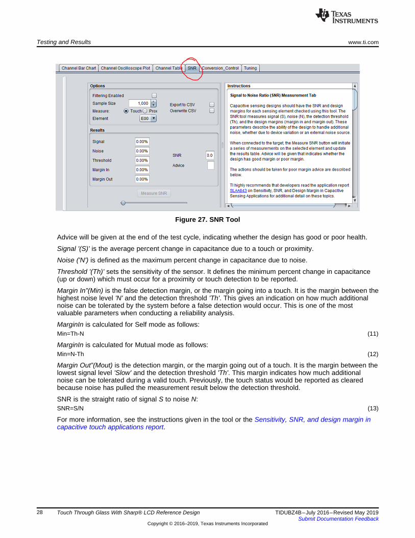
Figure 27. SNR Tool
Advice will be given at the end of the test cycle, indicating whether the design has good or poor health.
Signal '(S)' is the average percent change in capacitance due to a touch or proximity.
Noise ('N') is defined as the maximum percent change in capacitance due to noise.
Threshold '(Th)' sets the sensitivity of the sensor. It defines the minimum percent change in capacitance(up or down) which must occur for a proximity or touch detection to be reported.
Margin In”(Min) is the false detection margin, or the margin going into a touch. It is the margin between thehighest noise level 'N' and the detection threshold 'Th'. This gives an indication on how much additionalnoise can be tolerated by the system before a false detection would occur. This is one of the mostvaluable parameters when conducting a reliability analysis.
MarginIn is calculated for Self mode as follows:Min=Th-N (11)
MarginIn is calculated for Mutual mode as follows:Min=N-Th (12)
Margin Out”(Mout) is the detection margin, or the margin going out of a touch. It is the margin between thelowest signal level 'Slow' and the detection threshold 'Th'. This margin indicates how much additionalnoise can be tolerated during a valid touch. Previously, the touch status would be reported as clearedbecause noise has pulled the measurement result below the detection threshold.
SNR is the straight ratio of signal S to noise N:SNR=S/N (13)
For more information, see the instructions given in the tool or the Sensitivity, SNR, and design margin incapacitive touch applications report.
www.ti.com Testing and Results
29TIDUBZ4B–July 2016–Revised May 2019Submit Documentation Feedback
Copyright © 2016–2019, Texas Instruments Incorporated
Touch Through Glass With Sharp® LCD Reference Design
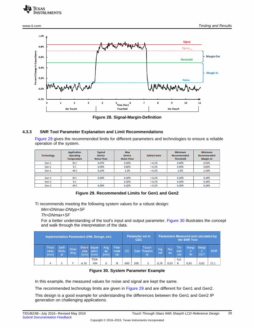
Figure 28. Signal-Margin-Definition
4.3.3 SNR Tool Parameter Explanation and Limit RecommendationsFigure 29 gives the recommended limits for different parameters and technologies to ensure a reliableoperation of the system.
Figure 29. Recommended Limits for Gen1 and Gen2
TI recommends meeting the following system values for a robust design:Min>DNmax-DNtyp+SFTh>DNmax+SFFor a better understanding of the tool’s input and output parameter, Figure 30 illustrates the conceptand walk through the interpretation of the data.
Figure 30. System Parameter Example
In this example, the measured values for noise and signal are kept the same.
The recommended technology limits are given in Figure 29 and are different for Gen1 and Gen2.
This design is a good example for understanding the differences between the Gen1 and Gen2 IPgeneration on challenging applications.
Testing and Results www.ti.com
30 TIDUBZ4B–July 2016–Revised May 2019Submit Documentation Feedback
Copyright © 2016–2019, Texas Instruments Incorporated
Touch Through Glass With Sharp® LCD Reference Design
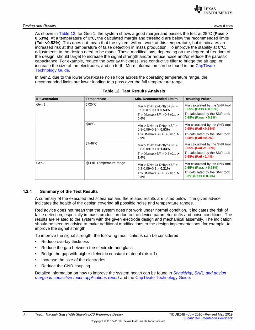
As shown in Table 12, for Gen 1, the system shows a good margin and passes the test at 25°C (Pass >0.53%). At a temperature of 0°C, the calculated margin and threshold are below the recommended limits(Fail <0.83%). This does not mean that the system will not work at this temperature, but it indicates anincreased risk at this temperature of false detection in mass production. To improve the stability at 0°C,adjustments to the design need to be made. These modifications, depending on the degree of freedom ofthe design, should target to increase the signal strength and/or reduce noise and/or reduce the parasiticcapacitance. For example, reduce the overlay thickness, use conductive filler to bridge the air gap, orincrease the size of the electrodes, and so forth. More information can be found in the CapTIvateTechnology Guide.
In Gen2, due to the lower worst-case noise floor across the operating temperature range, therecommended limits are lower leading to a pass over the full temperature range.
Table 12. Test Results Analysis
IP Generation Temperature Min. Recommended Limits Resulting ValuesGen 1 @25°C Min > DNmax-DNtyp+SF >
0.5-0.07+0.1 > 0.53%Th>DNmax+SF > 0.5+0.1 >0.6%
Min calculated by the SNR tool:0.65% (Pass > 0.53%)Th calculated by the SNR tool:0.68% (Pass > 0.6%)
@0°C Min > DNmax-DNtyp+SF >0.8-0.09+0.1 > 0.83%Th>DNmax+SF > 0.8+0.1 >0.9%
Min calculated by the SNR tool:0.65% (Fail <0.83%)Th calculated by the SNR tool:0.68% (Fail <0.9%)
@-40°C Min > DNmax-DNtyp+SF >0.8-0.09+0.1 > 1.33%Th>DNmax+SF > 0.8+0.1 >1.4%
Min calculated by the SNR tool:0.65% (Fail <1.33%)Th calculated by the SNR tool:0.68% (Fail <1.4%)
Gen2 @ Full Temperature range Min > DNmax-DNtyp+SF >0.2-0.09+0.1 > 0.21%Th>DNmax+SF > 0.2+0.1 >0.3%
Min calculated by the SNR tool:0.65% (Pass > 0.21%)Th calculated by the SNR tool:0.3% (Pass > 0.3%)
4.3.4 Summary of the Test ResultsA summary of the executed test scenarios and the related results are listed below. The given adviceindicates the health of the design covering all possible noise and temperature ranges.
Red advice does not mean that the system does not work under normal condition. It indicates the risk offalse detection, especially in mass production due to the device parameter drifts and noise conditions. Theresults are related to the system with the given electrode design and mechanical assembly. The indicationshould be seen as advice to make additional modifications to the design implementations, for example, toimprove the signal strength.
To improve the signal strength, the following modifications can be considered:• Reduce overlay thickness• Reduce the gap between the electrode and glass• Bridge the gap with higher dielectric constant material (air = 1)• Increase the size of the electrodes• Reduce the GND coupling
Detailed information on how to improve the system health can be found in Sensitivity, SNR, and designmargin in capacitive touch applications report and the CapTIvate Technology Guide.
www.ti.com Testing and Results
31TIDUBZ4B–July 2016–Revised May 2019Submit Documentation Feedback
Copyright © 2016–2019, Texas Instruments Incorporated
Touch Through Glass With Sharp® LCD Reference Design
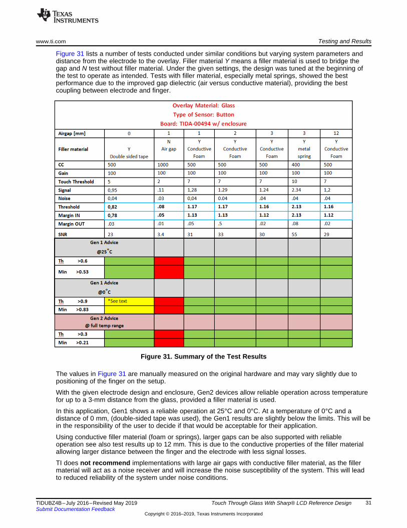
Figure 31 lists a number of tests conducted under similar conditions but varying system parameters anddistance from the electrode to the overlay. Filler material Y means a filler material is used to bridge thegap and N test without filler material. Under the given settings, the design was tuned at the beginning ofthe test to operate as intended. Tests with filler material, especially metal springs, showed the bestperformance due to the improved gap dielectric (air versus conductive material), providing the bestcoupling between electrode and finger.
Figure 31. Summary of the Test Results
The values in Figure 31 are manually measured on the original hardware and may vary slightly due topositioning of the finger on the setup.
With the given electrode design and enclosure, Gen2 devices allow reliable operation across temperaturefor up to a 3-mm distance from the glass, provided a filler material is used.
In this application, Gen1 shows a reliable operation at 25°C and 0°C. At a temperature of 0°C and adistance of 0 mm, (double-sided tape was used), the Gen1 results are slightly below the limits. This will bein the responsibility of the user to decide if that would be acceptable for their application.
Using conductive filler material (foam or springs), larger gaps can be also supported with reliableoperation see also test results up to 12 mm. This is due to the conductive properties of the filler materialallowing larger distance between the finger and the electrode with less signal losses.
TI does not recommend implementations with large air gaps with conductive filler material, as the fillermaterial will act as a noise receiver and will increase the noise susceptibility of the system. This will leadto reduced reliability of the system under noise conditions.
Testing and Results www.ti.com
32 TIDUBZ4B–July 2016–Revised May 2019Submit Documentation Feedback
Copyright © 2016–2019, Texas Instruments Incorporated
Touch Through Glass With Sharp® LCD Reference Design
NOTE: SF: Safety Factor, Min: MarginIn, DN: Device Noise, Th: Threshold, N: Noise measured bythe tool, MarginIn is calculated as follows: Min = Th - N
www.ti.com Design Files
33TIDUBZ4B–July 2016–Revised May 2019Submit Documentation Feedback
Copyright © 2016–2019, Texas Instruments Incorporated
Touch Through Glass With Sharp® LCD Reference Design
5 Design Files
5.1 SchematicsTo download the schematics, see the design files at TIDA-00494.
5.2 Bill of MaterialsTo download the bill of materials (BOM), see the design files at TIDA-00494.
5.3 PCB Layout RecommendationsThe diameter of the board is determined by the diameter of the enclosure window. On the upper part ofthe PCB, a board cutout has to be made for the LCD. It is important that all the components are surface-mounted devices (SMDs) and placed on the bottom part of the PCB so that the air gap between the toppart of the PCB and the window can be kept as small as possible. Only the buttons and the LED have tobe placed on the top part.
Digital signals can act as aggressors and can be active during capacitance measurement. Keep thesetypes of signals far away from the capacitive touch trace as shown for button 1, 3, and 4 of the TIDA-00494. If the digital signal and the capacitive touch trace must cross each other, like in the case of button2, then it is recommended to keep the crossing at a 90-degree angle.
Using a hatched ground plane on the top and bottom side reduces the parasitic capacitance associatedwith both trace and electrode capacitance, reducing the susceptibility of the traces to capacitive touchevents.
See the "Best Practices" section of the CapTIvate Technology Guide to browse other recommendationsfor an optimized layout.
5.3.1 Layout PrintsTo download the layer plots, see the design files at TIDA-00494.
5.4 Altium ProjectTo download the Altium project files, see the design files at TIDA-00494.
5.5 Gerber FilesTo download the Gerber files, see the design files at TIDA-00494.
5.6 Assembly DrawingsTo download the assembly drawings, see the design files at TIDA-00494.
Software Files www.ti.com
34 TIDUBZ4B–July 2016–Revised May 2019Submit Documentation Feedback
Copyright © 2016–2019, Texas Instruments Incorporated
Touch Through Glass With Sharp® LCD Reference Design
6 Software FilesTo download the software files, see the design files at TIDA-00494.
7 Related Documentation
1. Texas Instruments, CapTIvate™ Touch Microcontroller (http://www.ti.com/capTIvate)2. Texas Instruments, MSP CapTIvate MCU Development Kit (http://www.ti.com/tool/msp-capt-fr2633)3. Texas Instruments, MSP CapTIvate Design Center GUI (http://www.ti.com/tool/MSPCAPTDSNCTR)4. Texas Instruments, CapTIvate™ Technology Guide (http://software-
dl.ti.com/msp430/msp430_public_sw/mcu/msp430/CapTIvate_Design_Center/latest/exports/docs/users_guide/html/index.html)
5. Texas Instruments, MSP430FR2633 Product Page (http://www.ti.com/product/MSP430FR2633)6. Texas Instruments, Sharp® LCD BoosterPack (430BOOST-SHARP96) for the LaunchPad (SLAU553)7. Sharp Electronics, Application Information for Sharp’s LS013B4DN04 Memory LCD, SHARP LCD
Module Application Note(http://www.sharpmemorylcd.com/resources/ls013b4dn04_application_info.pdf)
7.1 TrademarksAll trademarks are the property of their respective owners.
8 About the AuthorGIOVANNI CAMPANELLA is an industrial systems engineer with the Field Transmitter Team in theFactory Automation and Control organization. He earned his bachelor's degree in electronic andtelecommunication engineering at the University of Bologna and his master's degree in electronicengineering at the Polytechnic of Turin in Italy. He is an expert in sensors and analog signal chain, with afocus on magnetic and analytics sensing technologies, and mixed-signal control of DC brushed servodrives. He is currently working on IoT and EH systems design for field transmitters and actuators.
www.ti.com Revision History
35TIDUBZ4B–July 2016–Revised May 2019Submit Documentation Feedback
Copyright © 2016–2019, Texas Instruments Incorporated
Revision History
Revision HistoryNOTE: Page numbers for previous revisions may differ from page numbers in the current version.
Changes from A Revision (September 2016) to B Revision .......................................................................................... Page
• Changed values in Finger Touch—Crosstalk table ................................................................................. 22• Changed values in Finger Touch With Gloves—Crosstalk table .................................................................. 24• Added CapTIvate Design Center SNR Tool section ................................................................................ 26
Changes from Original (July 2016) to A Revision ........................................................................................................... Page
• Changed from preview page............................................................................................................. 1
IMPORTANT NOTICE AND DISCLAIMER
TI PROVIDES TECHNICAL AND RELIABILITY DATA (INCLUDING DATASHEETS), DESIGN RESOURCES (INCLUDING REFERENCEDESIGNS), APPLICATION OR OTHER DESIGN ADVICE, WEB TOOLS, SAFETY INFORMATION, AND OTHER RESOURCES “AS IS”AND WITH ALL FAULTS, AND DISCLAIMS ALL WARRANTIES, EXPRESS AND IMPLIED, INCLUDING WITHOUT LIMITATION ANYIMPLIED WARRANTIES OF MERCHANTABILITY, FITNESS FOR A PARTICULAR PURPOSE OR NON-INFRINGEMENT OF THIRDPARTY INTELLECTUAL PROPERTY RIGHTS.These resources are intended for skilled developers designing with TI products. You are solely responsible for (1) selecting the appropriateTI products for your application, (2) designing, validating and testing your application, and (3) ensuring your application meets applicablestandards, and any other safety, security, or other requirements. These resources are subject to change without notice. TI grants youpermission to use these resources only for development of an application that uses the TI products described in the resource. Otherreproduction and display of these resources is prohibited. No license is granted to any other TI intellectual property right or to any thirdparty intellectual property right. TI disclaims responsibility for, and you will fully indemnify TI and its representatives against, any claims,damages, costs, losses, and liabilities arising out of your use of these resources.TI’s products are provided subject to TI’s Terms of Sale (www.ti.com/legal/termsofsale.html) or other applicable terms available either onti.com or provided in conjunction with such TI products. TI’s provision of these resources does not expand or otherwise alter TI’s applicablewarranties or warranty disclaimers for TI products.
Mailing Address: Texas Instruments, Post Office Box 655303, Dallas, Texas 75265Copyright © 2019, Texas Instruments Incorporated