topical review optical properties of iii-mn-v ...infrared.ucsd.edu/basov_pubs/120-burch jmmm 320...
TRANSCRIPT

ARTICLE IN PRESS
Journal of Magnetism and Magnetic Materials 320 (2008) 3207–3228
Contents lists available at ScienceDirect
Journal of Magnetism and Magnetic Materials
0304-88
doi:10.1
� Corr
E-m
journal homepage: www.elsevier.com/locate/jmmm
Topical review
Optical properties of III-Mn-V ferromagnetic semiconductors
K.S. Burch a,�, D.D. Awschalom b, D.N. Basov c
a Department of Physics, University of Toronto, Toronto, Ontario, Canada M5S 1A7b Department of Physics, University of California, Santa Barbara, CA 93106, USAc Department of Physics, University of California, San Diego, CA 92093-0319, USA
a r t i c l e i n f o
Article history:
Received 21 February 2008
Received in revised form
21 July 2008Available online 15 August 2008
Keywords:
Magnetic semiconductor
Optical property
Metal to insulator transition
53/$ - see front matter & 2008 Elsevier B.V. A
016/j.jmmm.2008.08.060
esponding author.
ail address: [email protected] (K.S.
a b s t r a c t
We review the first decade of extensive optical studies of ferromagnetic, III-Mn-V diluted magnetic
semiconductors. Mn introduces holes and local moments to the III–V host, which can result in carrier
mediated ferromagnetism in these disordered semiconductors. Spectroscopic experiments provide
direct access to the strength and nature of the exchange between holes and local moments; the degree
of itineracy of the carriers; and the evolution of the states at the Fermi energy with doping. Taken
together, the diversity of optical methods reveal that Mn is an unconventional dopant, in that the metal
to insulator transition is governed by the strength of the hybridization between Mn and its p-nictogen
neighbor. The interplay between the optical, electronic and magnetic properties of III-Mn-V magnetic
semiconductors is of fundamental interest and may enable future spin-optoelectronic devices.
& 2008 Elsevier B.V. All rights reserved.
1. Introduction
For more than two decades the study of magnetic impuritiesin semiconductors has received a great deal of attention(see Refs. [1–7] and references therein). The interest in thesecompounds is driven in part by the desire to utilize the spindegree of freedom in electronics [8–10]. This rapidly expandingfield of spin based electronics (spintronics) has exploited metalbased devices to bring about a revolution in magnetic sensors andcomputer hard drive density [11]. The discovery of ferromagnet-ism in III–V hosts heavily doped with Mn has launched a newphase in magnetic semiconductors research in part because of thehigh promise of III-Mn-V systems in the context of spintronicsapplications. The unique advantage of III-Mn-Vs is that magnetic,optical and electronic effects are all interconnected. Furthermore,all these properties are sensitive to external stimuli and can bereadily modified by the application of external electric ormagnetic field and also by illumination with light. Inherenttunability of (ferro)magnetic semiconductors is of high interest inview of novel magneto-optical device functionalities. Since opticaltechniques are well suited to create, measure and manipulatespins in semiconductors [12–18] the systematic investigation ofoptical properties of III-Mn-V materials promises to uncover newavenues for applications of ferromagnetic semiconductors byoffering insights into the fundamental physical processes in thesesystems.
ll rights reserved.
Burch).
Magnetic semiconductors also pose a number of uniquechallenges to understanding the physics governing their proper-ties. In addition to the ‘‘standard’’ difficulties with separatingelectron–electron interactions from disorder effects [19], mag-netic dopants result in additional states in the band structurewhose description is non-trivial [20]. Nonetheless they alsoprovide a rare opportunity to study the connections betweenband structure, carrier dynamics and magnetism in a well-controlled environment. Initially this work focused on II–VIcompounds and very dilute concentrations of transition metals(TM) doped into III–V semiconductors [1,2,6,21,22]. Research onthese diluted magnetic semiconductors (DMS) was limited by thedifficulty in doping carriers into II–VI compounds and the lowconcentration limit for TM in III–V materials [6]. The origin of thelimit in III–V semiconductors lies in the different lattice structuresfor the end members, namely zinc-blende or wurzite for III–Vcompounds and hexagonal for TM-V materials [23]. Nonethelessthis limitation has been overcome via growth under non-equilibrium conditions [24,25], resulting in a wide variety ofIII-TM-V compounds and heterostructures (including superlatticesand quantum wells) that exhibit magnetic order and can be tunedthrough their metal to insulator transition (MIT).
This advance has opened up a large array of possibleapplications for ferromagnetic III-Mn-V materials and led to anenormous amount of research. Despite the substantial progressover the past decade, there are still a number of open questions inthis field. In particular, the proper theoretical framework todescribe the ferromagnetism that emerges in many III-TM-Vmaterials still remains elusive [3,7,26–39]. The answer to thisfundamental question has been hindered by a lack of consensus

ARTICLE IN PRESS
K.S. Burch et al. / Journal of Magnetism and Magnetic Materials 320 (2008) 3207–32283208
about the evolution of the electronic structure of III-TM-Vcompounds with TM doping. A goal of this review is to offer thereader an in-depth discussion of this fundamental, yet contro-versial issue. In this vain, we have based our discussion on theinformation that has emerged from a variety of spectroscopicexperiments with an emphasis on data generated throughextensive optical studies of III-Mn-V materials.
Optical techniques have established themselves as providingkey insights into the band structure of materials. In fact, theelectronic structure of many semiconductors has been determinedby comparing theoretical calculations to optical results [40].Furthermore, as summarized in Fig. 1, optical techniques cover abroad range of energy scales in magnetic semiconductors. Inaddition, optical studies have provided a unique view into theunderlying physics governing various correlated electron materi-als [41–45]. Similar to these systems III-TM-V semiconductors alsoexhibit an interplay between their magnetic properties, carrierdynamics and band structure. Interestingly in III-TM-V DMS thecarriers originate from the magnetic ions but also mediate thelong-range magnetic interaction by traversing the host lattice.This arises from the mixing of the local moments with extendedstates. In fact, this hybridization between p and d orbitals is whatdistinguishes III-TM-V compounds from semiconductors dopedwith non-magnetic impurities.
To better understand the effects of magnetism on the bandstructure of III–V semiconductors (and vice versa) extensiveoptical studies have been applied to III-Mn-V ferromagneticDMS. As detailed throughout this review, magneto-opticalexperiments have demonstrated the ferromagnetism originatesfrom a single III-Mn-V phase and not from inclusions, such asMn-V in a III–V matrix. Furthermore, magneto-optical measure-ments have provided a determination of the strength of thehybridization between the Mn local moments and holes thatmediate the magnetic state [2,3,22,46,47]. As far as the evolutionof the electronic structure with Mn doping is concerned, opticalspectroscopy has uncovered a number of fundamental distinc-tions with the properties triggered by non-magnetic impurities inthe III–V series. In particular, the electromagnetic response ofsome heavily doped III-Mn-Vs that reveal a metallic state is instark contrast to the optical properties of non-magnetic counter-
1E-4
Crystal Field SplittingSpin-Orbit
Cyclotron Resonance
Zeeman EnergyQD Confinement
Quantum Dot CR
cm-1
THz
μm
2DEG:Plasmons DMS 1/τ1/ τ Non-Magnetic
Mobility Gap
2DEG: EF
Mn Acceptor LevelPhonons
Mobility GapeV
Visible
MagneticPolarons
Exchange
As Ga
Fiber-Telecom.
10000
0.1
1
Band Gap
1000100101
10000100010010
1101001000
10.10.011E-3
Fig. 1. Energy scales in semiconductors covered by optical techniques, with 1=tthe free carrier scattering rate, EF the Fermi energy. The abbreviations QD, CR,
DMS, and 2DEG refer to quantum dot, cyclotron resonance, diluted magnetic
semiconductor, and two-dimensional electron gas, respectively.
parts. It is our intention to present a brief overview of theinvestigation of the optical properties of III-Mn-V semiconductorsat the time of the completion of this paper. The review is intendedto help the readers, especially those who are not spectroscopyexperts, to navigate through the vast literature as well as to learnabout both resolved and outstanding problems.
1.1. Theoretical background
One of the earliest successes of quantum mechanics was theexplanation of the role of the band structure in separating metalsfrom insulators. There are many examples in the literature wherea material is tuned from one of these diametrically opposed statesto the other. Understanding MITs continues to be a centralchallenge not only in the study of doped semiconductors, butto many areas of contemporary condensed matter physics[19,44,48–51]. Since the long-range magnetic order in magneticsemiconductors often emerges close to the metallic state, acomplete description of the MIT appears important to fullyunderstanding the ferromagnetism in III-Mn-V semiconductors.We therefore begin by discussing our current understanding ofthe MIT of semiconductors doped with non-magnetic, chargedimpurities. The discussion will focus on the implications for theelectronic structure of traversing a MIT, as well as what role theband structure plays in the MIT. This section is meant to simplygive the reader a basic overview of this complex topic, a morecomplete discussion can be found in Refs. [44,48–51].
Let us begin by considering the effect of doping a singlecharged impurity, namely an acceptor that introduces a hole intothe system. Since the acceptor will gain one electron frombonding with its neighbors, the hole will experience a Coulombattraction to the acceptor, thereby behaving like a hydrogen atom.However, since the semiconductor is highly polarizable, it willscreen the charge significantly. As a result, new states form in theband gap of the semiconductor that correspond to the states of abound electron in a hydrogen atom whose energies have beenreduced by a factor of ðmVB=meÞ1=�2, where mVB is the effectivemass of holes in the valence band (VB), me is the free electronmass and � is the static dielectric constant. In fact, a whole seriesof states will form, that correspond to the screened states of ahydrogen atom, often referred to as the Lyman series and labeledas in atomic spectra (1s, 2s, 2p, etc.).
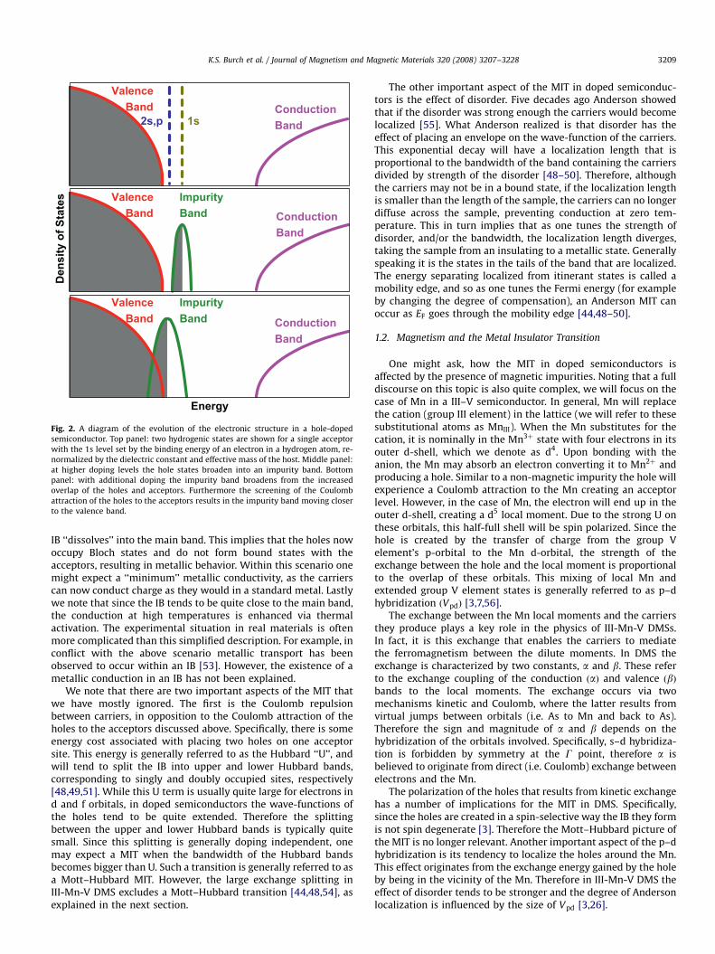
At very low doping levels and in the limit T ! 0, the holesdonated by the acceptors occupy hydrogenic bound states. Thismeans the doped semiconductor will still be an insulator (i.e. zerodc conductivity, sdc, in the limit of zero temperature). Early in thestudy of doped semiconductors, Mott pointed out that these statesare modified as the dopant density is increased. With additionaloverlap the states will start to broaden into an ‘‘impurity band’’(IB) [52]. Initially the IB will be near the 1s state of the originalacceptor and its width will be defined, in part, by the averageoverlap of the holes on different acceptor sites (see Fig. 2). Since,generally speaking, there is no exchange splitting in non-magneticsemiconductors the IB will be half-filled, therefore one mightexpect metallic behavior as soon as an IB is well formed. However,the separation of the IB from the VB indicates that there is stillsome Coulomb attraction between the holes and the acceptors.This implies that at zero temperature a bound state can always beformed and the material remains an insulator. Furthermore theCoulomb repulsion between the holes as well as the disorderinevitable in any doped system will likely lead to localization ofthe hole states.
The metallic transport in doped semiconductors is believed tooccur via the assumption that once the Coulomb attractionbetween the holes and the acceptors is completely screened the
ARTICLE IN PRESS
2s,p 1s
Valence Band Conduction
Band
Energy
ImpurityBand
Valence Band Conduction
Band
Den
sity
of S
tate
s ImpurityBand
Valence Band Conduction
Band
Fig. 2. A diagram of the evolution of the electronic structure in a hole-doped
semiconductor. Top panel: two hydrogenic states are shown for a single acceptor
with the 1s level set by the binding energy of an electron in a hydrogen atom, re-
normalized by the dielectric constant and effective mass of the host. Middle panel:
at higher doping levels the hole states broaden into an impurity band. Bottom
panel: with additional doping the impurity band broadens from the increased
overlap of the holes and acceptors. Furthermore the screening of the Coulomb
attraction of the holes to the acceptors results in the impurity band moving closer
to the valence band.
K.S. Burch et al. / Journal of Magnetism and Magnetic Materials 320 (2008) 3207–3228 3209
IB ‘‘dissolves’’ into the main band. This implies that the holes nowoccupy Bloch states and do not form bound states with theacceptors, resulting in metallic behavior. Within this scenario onemight expect a ‘‘minimum’’ metallic conductivity, as the carrierscan now conduct charge as they would in a standard metal. Lastlywe note that since the IB tends to be quite close to the main band,the conduction at high temperatures is enhanced via thermalactivation. The experimental situation in real materials is oftenmore complicated than this simplified description. For example, inconflict with the above scenario metallic transport has beenobserved to occur within an IB [53]. However, the existence of ametallic conduction in an IB has not been explained.
We note that there are two important aspects of the MIT thatwe have mostly ignored. The first is the Coulomb repulsionbetween carriers, in opposition to the Coulomb attraction of theholes to the acceptors discussed above. Specifically, there is someenergy cost associated with placing two holes on one acceptorsite. This energy is generally referred to as the Hubbard ‘‘U’’, andwill tend to split the IB into upper and lower Hubbard bands,corresponding to singly and doubly occupied sites, respectively[48,49,51]. While this U term is usually quite large for electrons ind and f orbitals, in doped semiconductors the wave-functions ofthe holes tend to be quite extended. Therefore the splittingbetween the upper and lower Hubbard bands is typically quitesmall. Since this splitting is generally doping independent, onemay expect a MIT when the bandwidth of the Hubbard bandsbecomes bigger than U. Such a transition is generally referred to asa Mott–Hubbard MIT. However, the large exchange splitting inIII-Mn-V DMS excludes a Mott–Hubbard transition [44,48,54], asexplained in the next section.
The other important aspect of the MIT in doped semiconduc-tors is the effect of disorder. Five decades ago Anderson showedthat if the disorder was strong enough the carriers would becomelocalized [55]. What Anderson realized is that disorder has theeffect of placing an envelope on the wave-function of the carriers.This exponential decay will have a localization length that isproportional to the bandwidth of the band containing the carriersdivided by strength of the disorder [48–50]. Therefore, althoughthe carriers may not be in a bound state, if the localization lengthis smaller than the length of the sample, the carriers can no longerdiffuse across the sample, preventing conduction at zero tem-perature. This in turn implies that as one tunes the strength ofdisorder, and/or the bandwidth, the localization length diverges,taking the sample from an insulating to a metallic state. Generallyspeaking it is the states in the tails of the band that are localized.The energy separating localized from itinerant states is called amobility edge, and so as one tunes the Fermi energy (for exampleby changing the degree of compensation), an Anderson MIT canoccur as EF goes through the mobility edge [44,48–50].
1.2. Magnetism and the Metal Insulator Transition
One might ask, how the MIT in doped semiconductors isaffected by the presence of magnetic impurities. Noting that a fulldiscourse on this topic is also quite complex, we will focus on thecase of Mn in a III–V semiconductor. In general, Mn will replacethe cation (group III element) in the lattice (we will refer to thesesubstitutional atoms as MnIII). When the Mn substitutes for thecation, it is nominally in the Mn3þ state with four electrons in itsouter d-shell, which we denote as d4. Upon bonding with theanion, the Mn may absorb an electron converting it to Mn2þ andproducing a hole. Similar to a non-magnetic impurity the hole willexperience a Coulomb attraction to the Mn creating an acceptorlevel. However, in the case of Mn, the electron will end up in theouter d-shell, creating a d5 local moment. Due to the strong U onthese orbitals, this half-full shell will be spin polarized. Since thehole is created by the transfer of charge from the group Velement’s p-orbital to the Mn d-orbital, the strength of theexchange between the hole and the local moment is proportionalto the overlap of these orbitals. This mixing of local Mn andextended group V element states is generally referred to as p–dhybridization ðVpdÞ [3,7,56].
The exchange between the Mn local moments and the carriersthey produce plays a key role in the physics of III-Mn-V DMSs.In fact, it is this exchange that enables the carriers to mediatethe ferromagnetism between the dilute moments. In DMS theexchange is characterized by two constants, a and b. These referto the exchange coupling of the conduction ðaÞ and valence ðbÞbands to the local moments. The exchange occurs via twomechanisms kinetic and Coulomb, where the latter results fromvirtual jumps between orbitals (i.e. As to Mn and back to As).Therefore the sign and magnitude of a and b depends on thehybridization of the orbitals involved. Specifically, s–d hybridiza-tion is forbidden by symmetry at the G point, therefore a isbelieved to originate from direct (i.e. Coulomb) exchange betweenelectrons and the Mn.
The polarization of the holes that results from kinetic exchangehas a number of implications for the MIT in DMS. Specifically,since the holes are created in a spin-selective way the IB they formis not spin degenerate [3]. Therefore the Mott–Hubbard picture ofthe MIT is no longer relevant. Another important aspect of the p–dhybridization is its tendency to localize the holes around the Mn.This effect originates from the exchange energy gained by the holeby being in the vicinity of the Mn. Therefore in III-Mn-V DMS theeffect of disorder tends to be stronger and the degree of Andersonlocalization is influenced by the size of Vpd [3,26].

ARTICLE IN PRESS
K.S. Burch et al. / Journal of Magnetism and Magnetic Materials 320 (2008) 3207–32283210
The tendency of the holes to localize around the Mn also hasimportant implications for the electronic structure of the III-Mn-VDMS. Specifically the binding energy of the hole will not onlyinclude its Coulomb attraction to the Mn nucleus but also thestrength of Vpd. Therefore the IB tends to be significantly furtheraway from the VB than in other p-type III–V semiconductors [57].Another interesting implication of the hybridization between theholes and the Mn local moment is its effect on the nature of thestates in the IB. In particular, it has been suggested that this IB willnot originate only from the states taken from the VB (primarilyp-like states of the group V element), but the IB may also acquired-orbital character from the Mn. The degree of Mn character in theIB will be determined by the strength of Vpd [31,32,58–61]. Sincethe IB is no longer simply derived from VB states, this suggeststhat if the hybridization is strong enough the standard picture ofan IB that merges back into the main band upon the MIT[44,48–50] may need to be modified. This concept can be checkedby tuning the lattice constant (and in turn the hybridizationbetween Mn and the group V element), while simultaneouslymonitoring the strength of the exchange and examining theelectronic structure. As we will detail, optical studies suggest thatthe exchange is stronger in materials with smaller latticeconstants. Furthermore the IB appears to persist on the metallicside of the MIT in some of these compounds (see Section 3.1).Provided Vpd is strong enough, then the Mn d states end up insidethe band gap of the semiconductor, such that the hole remains ina Mn d-level. This implies that for strong enough Vpd, Mn remainsin the d4 configuration (see Sections 5.2 and 5.3).
2. In1�xMnxAs
Munekata and collaborators were the first to overcome theapparent intrinsic doping limits of Mn in III–V semiconductors bygrowing In1�xMnxAs under non-equilibrium conditions using lowtemperature molecular beam epitaxy (LT-MBE) [24]. This quicklyled to the first realization by Ohno et al. of a ferromagnetic III–VDMS [62]. It was also found that the samples could be prepared asn-type or p-type depending on growth conditions, however, onlythe p-type films exhibited ferromagnetic behavior. InAs has thelargest lattice constant of all of the III-Mn-V systems, and there-fore should have the smallest value of exchange (see Section 1.2).The ferromagnetic transition temperatures ðTCÞ of In1�xMnxAscompounds tend to be somewhat lower than in other III-Mn-Vs(i.e. TCo90 K) [63,64].
2.1. Cyclotron resonance in In1�xMnxAs
Since determining the nature of the holes in III-Mn-V DMS is akey to understanding the physics underlying their magnetic order,cyclotron resonance (CR) experiments emerged as an importantprobe of these compounds. In fact, the first CR experiments insemiconductors were also the first verification of the validity ofthe quasi-particle concept, which is a cornerstone of the Fermiliquid theory. In these measurements, the microwave absorptionwas monitored in Ge [65]. In this case the carriers were opticallyexcited into the conduction and VBs resulting in strong absorptionat the appropriate cyclotron frequencies ðocÞ. The cyclotronfrequency depends directly on the band mass mB of the quasi-particles (oc ¼ eB=mBc), where e is the free electron charge, B theapplied magnetic field, and c is the speed of light. Therefore bymeasuring the absorption at a fixed frequency and sweeping themagnetic field (note that the external radiation must propagatealong the direction of applied magnetic field) one will observe anabsorption at a B determined by mB. Thus Dresslhaus et al.’sobservation of a cyclotron absorption at fields much higher than
what would be expected for free electrons, demonstrated that thecarriers in Ge and Si moved with a band mass significantly smallerthan me.
It is interesting to note that despite the potential importance ofcyclotron measurements to the understanding of III-Mn-Vmagnetic semiconductors, these experiments were not reporteduntil 2002. So far CR has only been observed in In1�xMnxAs. Whilethis might seem surprising, one must keep in mind that for a CRpeak to be observed the condition: oc41=t must be satisfied,where 1=t is the scattering rate of the carriers. Since III-Mn-Vmaterials contain significant numbers of defects, overcoming theoc41=t condition requires very large magnetic fields (between50 and 500 T). Another useful aspect of CR experiments is that thescattering rate can be determined from the width of theabsorption peak. The CR of In1�xMnxAs was first measured in ann-type, paramagnetic sample [66]. A resonant feature that shiftsto lower B and broadens as the amount of Mn is increased wasobserved in this experiment. These results indicated a reductionof the electron band mass (approximately 25% for x ¼ 0:12) andincreased disorder. While this study did not directly address thenature of the carriers that mediate the ferromagnetism inIn1�xMnxAs, it was able to determine the value of the exchangethrough direct comparison with theoretical predictions.
In general it is expected that the exchange integrals N0aðbÞwillaffect the shape of the conduction (valence) band as well as theband gap. Therefore the band mass of the carriers that reside inthese bands will be sensitive to the strength of the exchange. Sincethe initial CR measurements only determined the electron mass inn-type In1�xMnxAs, one might expect these measurements areonly sensitive to a. However, since InAs has a fairly small bandgap, there is strong mixing between the conduction and VB states.It is also important to note that in the k � p theory, the mass in agiven band is proportional to the band gap (due to the amount ofmixing of s and p states). To take these effects into account atheoretical model based on a k � p approach including the effectsof a and b [30] was used to explain the data of Fumagalli et al. Theresults of this model fit the data well, and suggest that theprimary effect of the exchange is to reduce the band gap, therebyreducing the band mass. Indeed measurements of the mid-infrared (MIR) absorption (see Section 2.2) confirmed a reductionin the band gap with the introduction of Mn [30]. Interestingly theexperimental results could only be properly modeled by settinga ¼ 0:5 eV and b ¼ �1:0 eV.
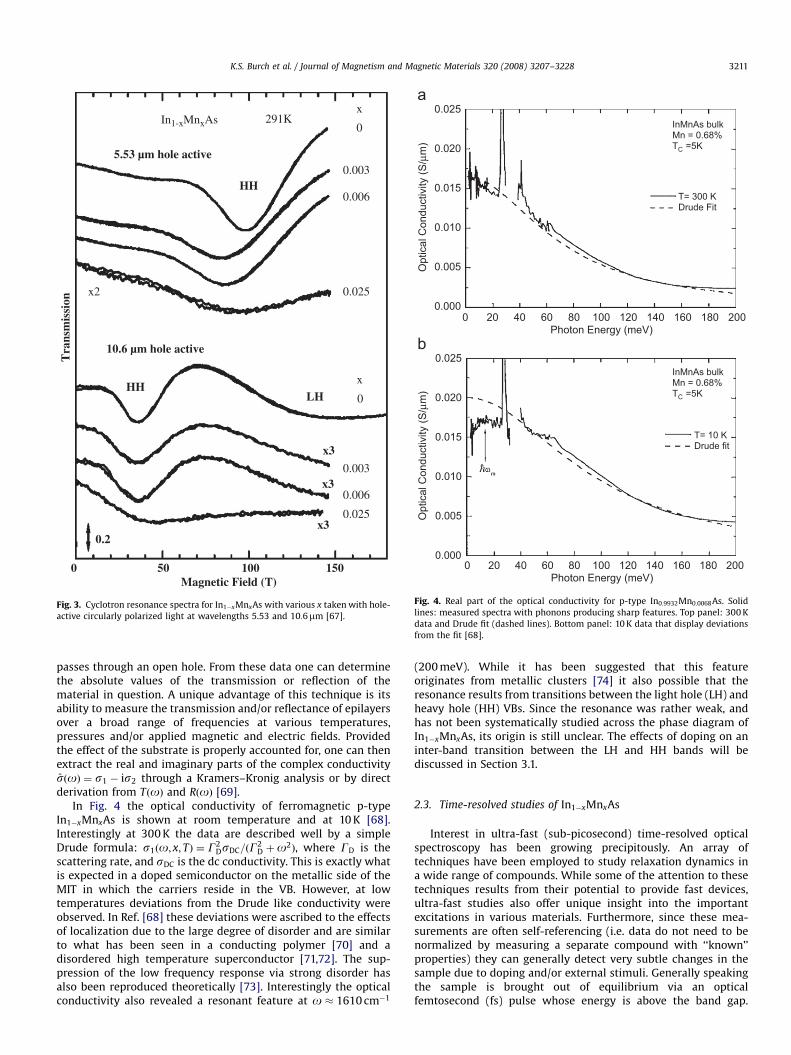
Given the small value of the hybridization in In1�xMnxAs, onemight expect the holes to reside in the valance band. Experi-mental confirmation of this expectation by means of CR measure-ments of p-type In1�xMnxAs was exceedingly difficult since holestend to have larger masses than electrons. Indeed, the firstmeasurements of hole CR in In1�xMnxAs, shown in Fig. 3, requiredfields up to 500 T, and were performed at multiple wavelengths[67]. These comprehensive studies revealed that the carriershave masses only consistent with conduction in the InAs VB,and determined the cyclotron mobilities between 800 and200 cm2=Vs. Interestingly, unlike the n-type case, the mass didnot depend on Mn doping. This also suggests that the carriers arep-type and not strongly effected by the p–d hybridization.
2.2. Optical conductivity of In1�xMnxAs
Infrared spectroscopy is another extremely powerful tool forstudying the properties of III-Mn-V DMS. In these experimentsone detects the intensity of the light from a spectrometer that iseither transmitted through or reflected from the sample on thesubstrate and then normalizes it by the intensity of the light thatpasses through or is reflected from an equivalent substrate or
ARTICLE IN PRESS
In1-xMnxAs 291Kx
0
0.003
0.006
0.025
5.53 µm hole active
10.6 µm hole active
x2
HH
HHLH 0
x
0.003
0.006
0.025
x3
x3
x30.2
0Magnetic Field (T)
Tra
nsm
issi
on
15010050
Fig. 3. Cyclotron resonance spectra for In1�xMnxAs with various x taken with hole-
active circularly polarized light at wavelengths 5.53 and 10:6mm [67].
0.025
0.020
0.015
0.010
0.000
0.005
0.025
0.020
0.015
0.010
0.000
0.005
Opt
ical
Con
duct
ivity
(S/μ
m)
Opt
ical
Con
duct
ivity
(S/μ
m)
0Photon Energy (meV)
Photon Energy (meV)
T= 300 KDrude Fit
T= 10 KDrude fit
InMnAs bulkMn = 0.68%TC =5K
InMnAs bulkMn = 0.68%TC =5K
20018016014012010080604020
0 20018016014012010080604020
Fig. 4. Real part of the optical conductivity for p-type In0:9932Mn0:0068As. Solid
lines: measured spectra with phonons producing sharp features. Top panel: 300 K
data and Drude fit (dashed lines). Bottom panel: 10 K data that display deviations
from the fit [68].
K.S. Burch et al. / Journal of Magnetism and Magnetic Materials 320 (2008) 3207–3228 3211
passes through an open hole. From these data one can determinethe absolute values of the transmission or reflection of thematerial in question. A unique advantage of this technique is itsability to measure the transmission and/or reflectance of epilayersover a broad range of frequencies at various temperatures,pressures and/or applied magnetic and electric fields. Providedthe effect of the substrate is properly accounted for, one can thenextract the real and imaginary parts of the complex conductivitysðoÞ ¼ s1 � is2 through a Kramers–Kronig analysis or by directderivation from TðoÞ and RðoÞ [69].
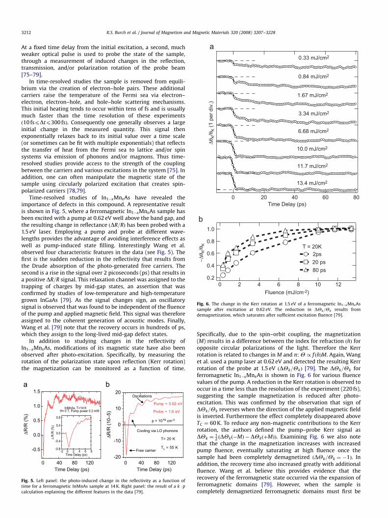
In Fig. 4 the optical conductivity of ferromagnetic p-typeIn1�xMnxAs is shown at room temperature and at 10 K [68].Interestingly at 300 K the data are described well by a simpleDrude formula: s1ðo; x; TÞ ¼ G2
DsDC=ðG2D þo2Þ, where GD is the
scattering rate, and sDC is the dc conductivity. This is exactly whatis expected in a doped semiconductor on the metallic side of theMIT in which the carriers reside in the VB. However, at lowtemperatures deviations from the Drude like conductivity wereobserved. In Ref. [68] these deviations were ascribed to the effectsof localization due to the large degree of disorder and are similarto what has been seen in a conducting polymer [70] and adisordered high temperature superconductor [71,72]. The sup-pression of the low frequency response via strong disorder hasalso been reproduced theoretically [73]. Interestingly the opticalconductivity also revealed a resonant feature at o � 1610 cm�1
(200 meV). While it has been suggested that this featureoriginates from metallic clusters [74] it also possible that theresonance results from transitions between the light hole (LH) andheavy hole (HH) VBs. Since the resonance was rather weak, andhas not been systematically studied across the phase diagram ofIn1�xMnxAs, its origin is still unclear. The effects of doping on aninter-band transition between the LH and HH bands will bediscussed in Section 3.1.
2.3. Time-resolved studies of In1�xMnxAs
Interest in ultra-fast (sub-picosecond) time-resolved opticalspectroscopy has been growing precipitously. An array oftechniques have been employed to study relaxation dynamics ina wide range of compounds. While some of the attention to thesetechniques results from their potential to provide fast devices,ultra-fast studies also offer unique insight into the importantexcitations in various materials. Furthermore, since these mea-surements are often self-referencing (i.e. data do not need to benormalized by measuring a separate compound with ‘‘known’’properties) they can generally detect very subtle changes in thesample due to doping and/or external stimuli. Generally speakingthe sample is brought out of equilibrium via an opticalfemtosecond (fs) pulse whose energy is above the band gap.
ARTICLE IN PRESS
−Δθ K
/θK
Fluence (mJ/cm-2)
T = 20K 2ps 20 ps 80 ps
ΔθK/θ
K (1
per
div
.)Time Delay (ps)
0.33 mJ/cm2
0.84 mJ/cm2
1.67 mJ/cm2
3.34 mJ/cm2
6.68 mJ/cm2
10.0 mJ/cm2
11.7 mJ/cm2
13.4 mJ/cm2
806040200
1.0
0.8
0.6
0.4
0.2121086420
Fig. 6. The change in the Kerr rotation at 1.5 eV of a ferromagnetic In1�xMnxAs
sample after excitation at 0.62 eV. The reduction in DYk=Yk results from
demagnetization, which saturates after sufficient excitation fluence [79].
K.S. Burch et al. / Journal of Magnetism and Magnetic Materials 320 (2008) 3207–32283212
At a fixed time delay from the initial excitation, a second, muchweaker optical pulse is used to probe the state of the sample,through a measurement of induced changes in the reflection,transmission, and/or polarization rotation of the probe beam[75–79].
In time-resolved studies the sample is removed from equili-brium via the creation of electron–hole pairs. These additionalcarriers raise the temperature of the Fermi sea via electron–electron, electron–hole, and hole–hole scattering mechanisms.This initial heating tends to occur within tens of fs and is usuallymuch faster than the time resolution of these experimentsð10 fspDtp300 fsÞ. Consequently one generally observes a largeinitial change in the measured quantity. This signal thenexponentially relaxes back to its initial value over a time scale(or sometimes can be fit with multiple exponentials) that reflectsthe transfer of heat from the Fermi sea to lattice and/or spinsystems via emission of phonons and/or magnons. Thus time-resolved studies provide access to the strength of the couplingbetween the carriers and various excitations in the system [75]. Inaddition, one can often manipulate the magnetic state of thesample using circularly polarized excitation that creates spin-polarized carriers [78,79].
Time-resolved studies of In1�xMnxAs have revealed theimportance of defects in this compound. A representative resultis shown in Fig. 5, where a ferromagnetic In1�xMnxAs sample hasbeen excited with a pump at 0.62 eV well above the band gap, andthe resulting change in reflectance ðDR=RÞ has been probed with a1.5 eV laser. Employing a pump and probe at different wave-lengths provides the advantage of avoiding interference effects aswell as pump-induced state filling. Interestingly Wang et al.observed four characteristic features in the data (see Fig. 5). Thefirst is the sudden reduction in the reflectivity that results fromthe Drude absorption of the photo-generated free carriers. Thesecond is a rise in the signal over 2 picoseconds (ps) that results ina positive DR=R signal. This relaxation channel was assigned to thetrapping of charges by mid-gap states, an assertion that wasconfirmed by studies of low-temperature and high-temperaturegrown InGaAs [79]. As the signal changes sign, an oscillatorysignal is observed that was found to be independent of the fluenceof the pump and applied magnetic field. This signal was thereforeassigned to the coherent generation of acoustic modes. Finally,Wang et al. [79] note that the recovery occurs in hundreds of ps,which they assign to the long-lived mid-gap defect states.
In addition to studying changes in the reflectivity ofIn1�xMnxAs, modifications of its magnetic state have also beenobserved after photo-excitation. Specifically, by measuring therotation of the polarization state upon reflection (Kerr rotation)the magnetization can be monitored as a function of time.
-20
-10
0
10
20
Probe = 1.6 eV
T= 20 K
Tc = 55 K
Pump = 0.62 eV
p = 1019 cm-3
ΔR
/R (%
)
Time Delay (ps)
InMnAs, T=14 K H= 0 T, Pump power 5.2 mW
0.8
0.4
0.0
-0.4
-0.8
Δ R
/R (%
)
86420-2Time Delay (ps)
Free carrier
Cooling via LO phonons
Oscillations1.5
1.0
0.5
0.0
-0.5
12080400Time Delay (ps)
12080400
ΔR/R
(10–
5)
Fig. 5. Left panel: the photo-induced change in the reflectivity as a function of
time for a ferromagnetic InMnAs sample at 14 K. Right panel: the result of a k � p
calculation explaining the different features in the data [79].
Specifically, due to the spin–orbit coupling, the magnetization(M) results in a difference between the index for refraction ð ~nÞ foropposite circular polarizations of the light. Therefore the Kerrrotation is related to changes in M and n: Y / f ð ~nÞM. Again, Wanget al. used a pump laser at 0.62 eV and detected the resulting Kerrrotation of the probe at 1.5 eV ðDYk=YkÞ [79]. The DYk=Yk forferromagnetic In1�xMnxAs is shown in Fig. 6 for various fluencevalues of the pump. A reduction in the Kerr rotation is observed tooccur in a time less than the resolution of the experiment (220 fs),suggesting the sample magnetization is reduced after photo-excitation. This was confirmed by the observation that sign ofDYk=Yk reverses when the direction of the applied magnetic fieldis inverted. Furthermore the effect completely disappeared aboveTC ¼ 60 K. To reduce any non-magnetic contributions to the Kerrrotation, the authors defined the pump–probe Kerr signal asDYk ¼
12 ðDYkð�MÞ �DYkðþMÞÞ. Examining Fig. 6 we also note
that the change in the magnetization increases with increasedpump fluence, eventually saturating at high fluence once thesample had been completely demagnetized ðDYk=Yk ¼ �1Þ. Inaddition, the recovery time also increased greatly with additionalfluence. Wang et al. believe this provides evidence that therecovery of the ferromagnetic state occurred via the expansion offerromagnetic domains [79]. However, when the sample iscompletely demagnetized ferromagnetic domains must first be
ARTICLE IN PRESS
K.S. Burch et al. / Journal of Magnetism and Magnetic Materials 320 (2008) 3207–3228 3213
nucleated before the recovery can begin. It is interesting to notethat despite the extensive work on the ultra-fast properties ofIn1�xMnxAs, all effects observed so far in this compound appear toresult from heating. Regardless, In1�xMnxAs could be very usefulfor magneto-optical storage devices.
2.4. Optical manipulation of magnetism in In1�xMnxAs
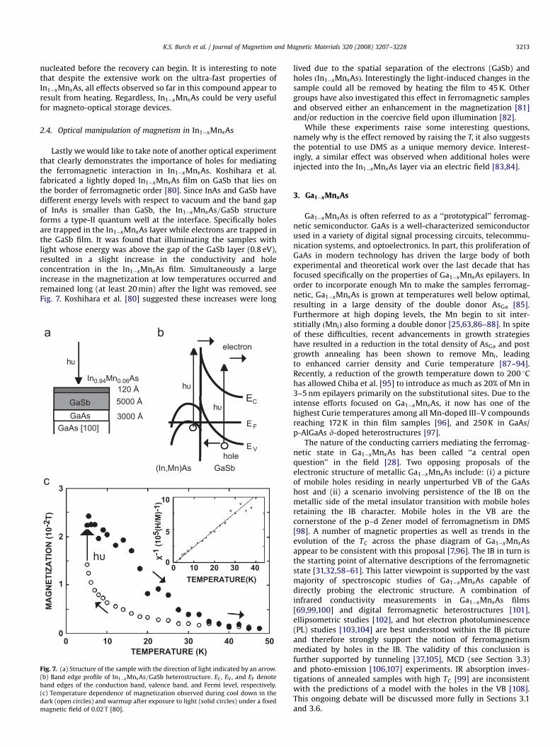
Lastly we would like to take note of another optical experimentthat clearly demonstrates the importance of holes for mediatingthe ferromagnetic interaction in In1�xMnxAs. Koshihara et al.fabricated a lightly doped In1�xMnxAs film on GaSb that lies onthe border of ferromagnetic order [80]. Since InAs and GaSb havedifferent energy levels with respect to vacuum and the band gapof InAs is smaller than GaSb, the In1�xMnxAs=GaSb structureforms a type-II quantum well at the interface. Specifically holesare trapped in the In1�xMnxAs layer while electrons are trapped inthe GaSb film. It was found that illuminating the samples withlight whose energy was above the gap of the GaSb layer (0.8 eV),resulted in a slight increase in the conductivity and holeconcentration in the In1�xMnxAs film. Simultaneously a largeincrease in the magnetization at low temperatures occurred andremained long (at least 20 min) after the light was removed, seeFig. 7. Koshihara et al. [80] suggested these increases were long
GaAsGaAs [100]
GaSb
In0.94Mn0.06As120 Å5000 Å
3000 Å
hυ
(In,Mn)As GaSb
hυ
hυ
hole
electron
EC
E F
E V
TEMPERATURE (K)
MA
GN
ETIZ
ATI
ON
(10-
2 T)
0
1
2
3
0 10 20
TEMPERATURE(K)
χ-1
(105
(H/M
)-1)
0 10 200
5
10
hυ
504030
4030
Fig. 7. (a) Structure of the sample with the direction of light indicated by an arrow.
(b) Band edge profile of In1�xMnxAs=GaSb heterostructure. EC, EV, and EF denote
band edges of the conduction band, valence band, and Fermi level, respectively.
(c) Temperature dependence of magnetization observed during cool down in the
dark (open circles) and warmup after exposure to light (solid circles) under a fixed
magnetic field of 0.02 T [80].
lived due to the spatial separation of the electrons (GaSb) andholes ðIn1�xMnxAsÞ. Interestingly the light-induced changes in thesample could all be removed by heating the film to 45 K. Othergroups have also investigated this effect in ferromagnetic samplesand observed either an enhancement in the magnetization [81]and/or reduction in the coercive field upon illumination [82].
While these experiments raise some interesting questions,namely why is the effect removed by raising the T, it also suggeststhe potential to use DMS as a unique memory device. Interest-ingly, a similar effect was observed when additional holes wereinjected into the In1�xMnxAs layer via an electric field [83,84].
3. Ga1�xMnxAs
Ga1�xMnxAs is often referred to as a ‘‘prototypical’’ ferromag-netic semiconductor. GaAs is a well-characterized semiconductorused in a variety of digital signal processing circuits, telecommu-nication systems, and optoelectronics. In part, this proliferation ofGaAs in modern technology has driven the large body of bothexperimental and theoretical work over the last decade that hasfocused specifically on the properties of Ga1�xMnxAs epilayers. Inorder to incorporate enough Mn to make the samples ferromag-netic, Ga1�xMnxAs is grown at temperatures well below optimal,resulting in a large density of the double donor AsGa [85].Furthermore at high doping levels, the Mn begin to sit inter-stitially ðMniÞ also forming a double donor [25,63,86–88]. In spiteof these difficulties, recent advancements in growth strategieshave resulted in a reduction in the total density of AsGa and postgrowth annealing has been shown to remove Mni, leadingto enhanced carrier density and Curie temperature [87–94].Recently, a reduction of the growth temperature down to 200 1Chas allowed Chiba et al. [95] to introduce as much as 20% of Mn in3–5 nm epilayers primarily on the substitutional sites. Due to theintense efforts focused on Ga1�xMnxAs, it now has one of thehighest Curie temperatures among all Mn-doped III–V compoundsreaching 172 K in thin film samples [96], and 250 K in GaAs/p-AlGaAs d-doped heterostructures [97].
The nature of the conducting carriers mediating the ferromag-netic state in Ga1�xMnxAs has been called ‘‘a central openquestion’’ in the field [28]. Two opposing proposals of theelectronic structure of metallic Ga1�xMnxAs include: (i) a pictureof mobile holes residing in nearly unperturbed VB of the GaAshost and (ii) a scenario involving persistence of the IB on themetallic side of the metal insulator transition with mobile holesretaining the IB character. Mobile holes in the VB are thecornerstone of the p–d Zener model of ferromagnetism in DMS[98]. A number of magnetic properties as well as trends in theevolution of the TC across the phase diagram of Ga1�xMnxAsappear to be consistent with this proposal [7,96]. The IB in turn isthe starting point of alternative descriptions of the ferromagneticstate [31,32,58–61]. This latter viewpoint is supported by the vastmajority of spectroscopic studies of Ga1�xMnxAs capable ofdirectly probing the electronic structure. A combination ofinfrared conductivity measurements in Ga1�xMnxAs films[69,99,100] and digital ferromagnetic heterostructures [101],ellipsometric studies [102], and hot electron photoluminescence(PL) studies [103,104] are best understood within the IB pictureand therefore strongly support the notion of ferromagnetismmediated by holes in the IB. The validity of this conclusion isfurther supported by tunneling [37,105], MCD (see Section 3.3)and photo-emission [106,107] experiments. IR absorption inves-tigations of annealed samples with high TC [99] are inconsistentwith the predictions of a model with the holes in the VB [108].This ongoing debate will be discussed more fully in Sections 3.1and 3.6.

ARTICLE IN PRESS
K.S. Burch et al. / Journal of Magnetism and Magnetic Materials 320 (2008) 3207–32283214
3.1. Broad-band optical studies of Ga1�xMnxAs
Spectroscopic ellipsometry experiments were pivotal in estab-lishing the electronic structure of standard semiconductors [40].Spectroscopic ellipsometry is particularly advantageous for thestudies of materials because the optical constants can bemeasured directly without recourse to Kramers–Kronig analysis.In addition one can often obtain information on oxide content andepilayer thicknesses. Ellipsometric studies of Ga1�xMnxAs focusedon the transformations upon Mn doping of the dielectricconstants ð�ðoÞ ¼ �1ðoÞ þ i�2ðoÞÞ above the band gap of the GaAshost [102]. A brief inspection of Fig. 8 shows unmistakablesimilarity in the gross features of the ellipsometric data betweenpristine GaAs and heavily doped epilayers with Mn concentrationsexceeding 7%. The characteristic structure in the spectra of �1ðoÞand �2ðoÞ are produced by inter-band transitions associatedwith van Hove singularities in the joint density of states labeledin Fig. 8 using a standard notation [40]. The band structure ofGa1�xMnxAs, including these transitions and important symmetrydirections is shown in Fig. 9. Importantly, E1, E00 and E2 features of
4
2
0
-2
-4
L Δ
+Δ1
Λ Γ
Γ8Γ6
Γ6
X
S.O
Mn A
Mn d5/d6
Mn d5/d4
E2
E0E0E1E1
L.H.H.H.
4
2
0
-2
-4
Ene
rgy
(eV
)
Wavevector k
Fig. 9. Left: GaAs band structure and relevant critical point transitions reproduced fro
while the lowest conduction band is labeled G6. The valence bands have been labeled as
filled ðd5=d4Þ and empty ðd5=d6
Þ levels are shown in gray, and the acceptor Mn A is das
L-point corresponds to the 111 direction and the X-point to the 001 direction. Right: th
-10
0
10
20
1
0
5
10
15
20
25
30
Energy (eV)
ε 1 GaAs Lt-GaAs Ga0.983Mn0.017As Ga0.972Mn0.028As Ga0.960Mn0.040As Ga0.948Mn0.052As Ga0.934Mn0.066As
ε 2
E2
E0
E1+ΔΔΔΔ1E1
E0
Energy (eV)
5432
1 5432 1 5432
1 5432
Fig. 8. The real and imaginary part of the dielectric function determined from
ellipsometric measurements at 292 K for a series of Ga1�xMnxAs thin films with
various concentrations of Mn. The plot also displays the optical constants for the
GaAs substrate and an LT-GaAs film. The critical points are labeled in the
conventional way and are primarily indicative of specific k-points. A broadening of
the E0 and E1 transitions with Mn doping is observed as well as the blue-shifting of
E1 feature (right panel). We also note the apparent lack of change in E00 and E2
transitions [102].
the GaAs host can all be recognized in the ellipsometry data forheavily doped Ga1�xMnxAs samples. This result attests to thequality of the Ga1�xMnxAs samples. Indeed, the above character-istic features are known to be wiped out in disordered semi-conductors [109].
Burch et al. [102] quantitatively studied the evolution of thecritical points with doping via an analysis of the second derivativespectra. This approach has the advantage of amplifying the subtlefeatures of the optical constants upon taking their derivatives.A significant blue-shifting of the E1 critical point was observed,while the position of all other critical points was unaffected by thepresence of Mn. The blue-shifting of E1 was attributed to thehybridization of the Mn IB with the GaAs VB [102]. Since the E1
critical point originates from transitions near the L-point (i.e. inthe 111 direction), the authors suggested that Vpd is k-dependent,which was recently confirmed by a combined experimental andtheoretical study of the electronic structure around a local Mnatom [111]. Since the Mn–As bond is along the 111 crystal-lographic direction (see Fig. 9), Vpd should be the strongest nearthe L-point [38,102].
It should be noted that Zhang and Das Sarma have recentlyshown that if Fermi energy resided in the VB, then a significantred-shifting of the fundamental band gap should be observed.Specifically, the Coulomb interaction between the holes wouldlead to a re-normalization of the critical points [28]. However, inMn-doped samples the fundamental band gap of GaAs ðE0Þ wasnot detected in the ellipsometry experiments, though this is notdue to the Mn doping per se. In fact the E0 structure is not seen isGaAs without any Mn when it is grown at low temperature.
The ellipsometry results presented in Ref. [102] provideadditional insights into the broadening of the band gap of GaAsgrown at low temperatures. In previous studies of these samples itwas determined that the broadening was, in part, the result oftransitions either beginning (in the case of n-type LT-GaAs) orending (in the case of p-type Ga1�xMnxAs) in the AsGa impuritystates [69]. Additional information provided by the �ðo41:5 eVÞ,suggested that the broadening of the fundamental gap also theresults from a relaxation of the requirement of momentumconservation. This relaxation is due to the presence of impuritiesthat provide additional scattering mechanisms. Since transitionsare no longer required to be direct, states in the VB that are not atthe zone center can contribute to transitions which end at thezone center. Ultimately this results in a broadening of transitionsand a transfer of spectral weight from higher energies to lowerones, as is seen in Fig. 8. We note that a similar result is found inGaAs damaged by ion-implantation [112]. Nonetheless, as dis-cussed in Section 3.3, MCD studies suggest that the fundamental
Ene
rgy
(eV
)
m Ref. [110]. The upper conduction bands are labeled as G7;8 based on symmetry,
HH for heavy-hole, LH for light-hole, and SO for split-off. Taken from Ref. [61], Mn d
hed-gray. The dispersion of the Mn acceptor level is also taken from Ref. [61]. The
e Ga1�xMnxAs unit cell with the important symmetry directions labeled.

ARTICLE IN PRESS
K.S. Burch et al. / Journal of Magnetism and Magnetic Materials 320 (2008) 3207–3228 3215
band gap of Ga1�xMnxAs only slightly blue-shifts with doping incontradiction to predictions of the VB scenario.
We now turn our attention to studies of the optical constantsbelow the fundamental band gap of the GaAs host. As pointed outabove, Mn doping leads to the formation of a metallic statein Ga1�xMnxAs films [25]. A counterpart infrared effect is adramatic change of the optical conductivity throughout theentire frequency range within the band gap of the GaAs host.These changes were first investigated by Nagai et al. [113] whoexamined the absorption coefficient. This study was later followedby an analysis of the optical conductivity of Ga1�xMnxAs by Singleyet al. [69,100]. Most recently, a comprehensive study of both asgrown and annealed films has been reported by Burch et al. [99](see Fig. 10). With the exception of one work, all Ga1�xMnxAssamples investigated so far using infrared methods were preparedusing LT-MBE. The only exception is the work of Seo et al. [114] infilms obtained using implantation of Mn ions into a GaAs film.
Ferromagnetic films of Ga1�xMnxAs grown by MBE reveal twonew features in the intra-gap conductivity. The first is a broadresonance initially centered at approximately 2000 cm�1, whosecenter energy is doping dependent. The second key feature is thepresence of finite conductivity in the limit of o! 0, signalingmetallic behavior. The oscillator strength of both featuresincreases with additional Mn doping. The primary impact ofannealing is to further increase the spectral weight of these twofeatures while their frequency dependence remains mostly
0
100
200
300
400
500
600102 103 104 102 103 104
ωp2=
p/m*
Lorentzian fit Drude fit Total fit Data
ω0
ω0
x=0.073annealed
x=0.052annealed
x=0.052
T= 7K
x=0.052
x=0.028x=0.040
σ 1(Ω
-1cm
-1)
x=0.073
Frequency (cm-1)
EF
Ene
rgy
Momentum
LH
HHEF
Fig. 10. (Bottom panels) Diagrams of the electronic structure of Ga1�xMnxAs
assuming EF lies in the light hole (LH) and heavy hole (HH) bands. (Left-bottom) at
low x, a transition occurs between the HH and LH bands. (Right-bottom) as the
carrier density is increased, EF moves farther into the LH and HH bands, causing
the transition to blue-shift. Top panels: the real part of the conductivity for a series
of Ga1�xMnxAs samples studied. An increase in s1ðoÞ occurs with larger Mn
concentration x and/or annealing. Top-right panel shows the results of fitting
s1ðoÞ for the annealed, x ¼ 0:052 sample using a Drude–Lorentz model [99].
unchanged. Due to the reduction in defect concentration, anneal-ing results in a slope in the conductivity for oo200 cm�1 asprescribed by the simple Drude model [99].
An observation of a resonance in the MIR is consistent witheither of the two fundamentally different views of the electronicstructure of Ga1�xMnxAs. Specifically assigning mobile holes atthe Fermi energy ðEFÞ to the IB or to the VB of the GaAs host willproduce a MIR feature. Indeed, if the holes reside in the IB the MIRresonance results from transitions between the IB and VB[27,31,32,36,58,59,115]. The 2000 cm�1 mode clearly seen in thetop-left panel of Fig. 10 occurs close to Lyman transitionsproduced by dilute concentrations of Mn in GaAs single crystals[116]. However, if EF lied in the VB of the GaAs host, then oneexpects a MIR resonance to result from transitions between theLH and HH bands. This latter interpretation was originallyproposed by Nagai et al. [113] and was followed up by calculationsincluding the role of disorder and a more realistic band structure[73,108,117]. In fact, calculations of the optical conductivitycarried out within the VB framework reproduce the shape of theexperimental data. Nevertheless one can discriminate betweenthe two scenarios by monitoring the doping dependence of theposition of the MIR peak.
As illustrated in the bottom panels of Fig. 10 the VB pictureimplies hardening of the resonance with increasing doping. Thisnatural conclusion is supported by the calculations of Sinova et al.within the VB scenario [108]. However, data reported by Burchet al. show a pronounced softening of the MIR resonance that isonly consistent with the IB model (see Fig. 2) [99]. Further supportfor the IB scenario originates from an analysis of the opticaleffective masses associated with the free carrier absorption. Thesemasses inferred from the oscillator strength sum rule yield m� onthe order of 10 times me [69,99,100]. These high masses should becontrasted with the VB mass (�0:38me [118]). Thus, metallicGa1�xMnxAs epilayers reveal the behavior in stark contrast to theexpectations of the VB scenario.
Jungwirth et al. [119] have proposed that the red-shift of theMIR resonance in Fig. 10 can be anticipated as a consequence ofincreased screening in samples with enhanced metalicity. Theauthors find support for this statement with finite-size exact-diagonalization calculations originally reported in Ref. [73]. Thesecalculations indeed show that a minute red-shift may occur insamples after a large reduction in disorder. A much morepronounced effect in these calculations is a dramatic narrowingof the MIR resonance that is required to reproduce a barelynoticeable red-shift. This is not consistent with experimentsrevealing red-shift without any significant modifications of thelineform. Furthermore, the data do not uncover any apparentempirical relationship between the position of the resonance andsDC that are anticipated within the framework of a proposal byJungwirth et al. [119]. On these grounds, we conclude that thedoping trends seen in the broad-band studies of electromagneticresponse of Ga1�xMnxAs cannot be reconciled with the calcula-tions based on the VB scenario.
It is worth pointing out that only the VB scenario of theelectronic response of Ga1�xMnxAs has reached the sophisticationrequired for detailed comparison with existing optical experi-ments. Considerably less effort has been dedicated so far to thetheoretical exploration of the properties implied by the IB picture.It remains to be seen if this latter picture can sustain similarexperimental scrutiny going beyond qualitative discussion ofproperties implied by the IB. As we will argue below a realisticpicture of electronic and magnetic properties of Ga1�xMnxAs mustaccount for coexistence of extended and localized properties ofMn-induced holes: a task that is beyond the existing theoreticalapproaches. We will return to the discussion of these issues inSection 3.6.
ARTICLE IN PRESS
A(2)ΔA0
σ- σ-R
aman
Inte
nsity
(a.u
.)
C
B
A
-Δex +Δex+Δex+Δex+Δex
(1)ΔA0
(2)ΔA0
(1)ΔA0
4Δd
3Δd
2ΔdΔd
σ+ σ -
*10
-1/2
+1/2
-5/2
-3/23d
(1)ΔA0
(2)ΔA0 +1
-1mF=0,±1
F=1
0σ- σ +
σ+ σ+
2Δd-h
sample B
a
b
c
605040302010
K.S. Burch et al. / Journal of Magnetism and Magnetic Materials 320 (2008) 3207–32283216
Ferromagnetism at high transition temperatures inGa1�xMnxAs occurs at extremely high Mn doping levels close tothe boundary where Mn begins to form clusters in the GaAs host.It is therefore important to address the issue of whether theoptical properties discussed above represent the intrinsic electro-magnetic response of Ga1�xMnxAs with Mn primarily enteringsubstitutionally in the GaAs lattice. This issue is particularlyimportant since some of the characteristic absorption featuresseen in Fig. 10 are consistent with the suggestion of amorphousMnAs clusters imbedded in low temperature grown GaAs(LT-GaAs). It has been reported that implantation of Mn ions inLT-GaAs films result in MnAs clusters that produce a resonantstructure reminiscent of the optical conductivity of Ga1�xMnxAsfilms grown by MBE [114]. However, in the implanted films theresonance is centered around 0.8 eV, and therefore appears to beinconsistent with what is found in the films grown by MBE. Finallywe note that if the feature seen in the MIR were due to metallicclusters inside the GaAs matrix, the resonance would be centered
at op=ffiffiffiffiffiffiffiffiffiffiffiffiffiffiffiffiffi2�h
1 þ 1q
where op is the plasma frequency of the metallic
cluster [114], which is proportional to the carrier density divided
by their mass, and �h1 is the dielectric constant of the host.
Therefore the red-shifting with doping would result from one oftwo unlikely scenarios: a decrease in op of the metallic spheres or
an increase in the dielectric constant.
0
C
B
+Δe+Δe
lase
r
4Δd3Δd
Raman Shift (cm-1)
Δe=geμBB+1/2
45403530252015105
Fig. 11. Raman spectra of Ga1�xMnxAs samples A (NMn ¼ 6� 1017 cm�3), B
(NMn ¼ 8� 1017 cm�3) and C (NMn ¼ 3:5� 1018 cm�3) measured in resonance
with the acceptor-exciton energy level. (a) The 2Dd2h feature in sample B is related
to the transition between the F ¼ 1 and 2 acceptor states at 0 (solid line) and 8 T.
(b) and (c) Stokes Raman spectra at 10 T for two circular polarization geometries,
labels are explained in the text. The inset in (b) shows the splitting of the F ¼ 1
acceptor ground state into Zeeman sub-levels. The inset in (c) illustrates the origin
of the satellite resonance labeled De in a two-step Raman process [120].
3.2. Light scattering studies of Ga1�xMnxAs
Inelastic light scattering has proven to be a useful techniquefor studying bosonic modes in a broad range of materials. Ingeneral a laser polarized along a specific crystallographic directionis reflected off the surface of a sample. The incoming photonsundergo a scattering event wherein they either absorb (Stokes) oremit (anti-Stokes) a boson in the sample, resulting in an energyshift of the reflected photon. By measuring a specific polarizationof the reflected light, one can select out different modes via theoptical selection rules. This technique, often called Ramanscattering, has measured the charge state of the Mn ion as afunction of x in Ga1�xMnxAs.
The first such study was performed on paramagneticGa1�xMnxAs single crystals grown by the Czochralski technique,
with Mn concentrations of 0:623:5� 1018 cm�3 [120]. Theauthors focused on spin-flip Raman scattering (SFRS) whereinthe spin of either the total angular momentum of the hole and Mncomplex or just that of the d-shell itself is changed. One expectsthe ground state of the total angular momentum of the Mn–hole
complex to be F ¼ jSd � Jhj ¼ 1, where Sd ¼52 is the total angular
momentum of the Mn d-shell and Jh ¼32 for the holes. This should
lead to features in the Raman spectra due to transitions from thejF ¼ 1;mF ¼ �1i level to the jF ¼ 2;mF ¼ �2i and jF ¼ 2;mF ¼ �1istates. In Fig. 11(a) a typical Raman spectra is shown with afeature due to a change in the angular momentum of the Mn–holecomplex from F ¼ 1 to 2 at 2Dd2h. It should be noted that theenergy of this resonance depends on the p–d exchange strength.
Interestingly by using different polarization configurations inmagnetic field additional features were observed in the Ramanspectra (see Fig. 11(b)). The center energy of these new resonancesshift linearly in field and tend to zero as the applied field isremoved. Spin flips of the acceptor that conserve the total angular
momentum are observed as two broad features labeled ð1;2ÞDA0
and shift with applied magnetic field as ð1;2Þ � gA0mBB, where
gA0¼ 2:74 is the g-factor of the acceptor, and mB the Bohr
magneton. The difference in their energy is related to whether
the flip is between states of DmF ¼ �1 or DmF ¼ �2. In the
samples with heavier doping levels these features disappear dueto the formation of the IB. However, the sharp features in thespectra labeled nDd, with n ¼ 1;2; . . . ; remain in samples withlarger Mn content and gain satellite features seen on the Stokesside (labeled þDe and Dex) and anti-Stokes side (at �Dex) withlarger Mn content. These resonances result from transitionswithin the Mn d-shell due to its interactions with the excitonsðDexÞ and photo-excited electrons ðþDeÞ created by the laser.Therefore one observes the flipping of the Mn spins Dd as well asthe exciton ðDexÞ and its electron ðDeÞ. Furthermore the number ofDd resonances depend on the number of Mn ions seen by theexciton. The field dependence of De and Dex is characteristic ofexcitons experiencing the external and exchange fields, andindicate the Mn ion is in a d5 state.
A later Raman study of MBE grown films focused on the effectsof increasing the Mn density. The 2Dd2h resonance was onlyobserved in samples with lower doping levels and its intensitywas significantly temperature dependent, which results fromthermal activation of the holes from the F ¼ 1 to F ¼ 2 statesand/or to the VB [121]. In addition, the intra-d-shell resonancewas observed in the samples with small Mn levels, but only above50 K, and its intensity was found to drop above 150 K. Thistemperature dependence is likely the result of the holes being

ARTICLE IN PRESS
K.S. Burch et al. / Journal of Magnetism and Magnetic Materials 320 (2008) 3207–3228 3217
tightly bound to the Mn at low temperatures, resulting in spinflips of the Mn–hole complex only. At higher temperatures theholes are thermally activated and spin-flips of the Mn ion emerge.Interestingly in the samples with heavier doping levels of Mn, the2Dd2h resonances disappeared and a new feature appeared at D2.This D2 feature was only observed for T490 K. From itstemperature and polarization dependence, Sapega et al. [121]conclude D2 is a transition within the Mn 5T2 levels that are splitby the dynamic Jahn–Teller effect. Such a transition is onlypossible if the Mn is in a d4 configuration, and therefore thesestudies suggest that with increasing concentration, the Mn goesfrom being in a d5 to d4 state. Furthermore Sapega et al. concludedthat the holes begin in acceptor levels with angular momentumJh ¼
32 but broaden into an IB.
Two recent Raman studies of Ga1�xMnxAs have taken analternate approach to the spectra [122,123]. They focused on theRaman spectra near the longitudinal (LO) and transverse (TO)optically active phonon modes. Both observed a mode due to acoupling between the LO phonon and free carrier plasmons, fromwhich they can extract the carrier densities. This technique isquite powerful as it can determine the carrier density accuratelywithout needing to apply large magnetic fields, as is required inHall measurements. Interestingly, one of these studies alsoobserved a shifting in the LO and TO modes, which they attributedto the alloying effect of Mn [123].
3.3. Magneto-optical studies of Ga1�xMnxAs
Insights into the exchange mechanism between the holes andlocal moments in DMS have been supplied by studies of theirmagneto-optical properties. Magneto-circular dichroism (MCD)measurements provide access to the Zeeman splitting of theconduction and VBs, such that the strength and nature of theexchange is determined [2]. In addition, magneto-optical techniqueshave been used to examine the domain structure and its evolutionupon magnetization reversal in Ga1�xMnxAs [124,125]. Further-more, it has been shown the magneto-optics are also quite powerfulfor studying the in-plane magnetization dynamics. Indeed, magne-to-linear dichroism where the difference between the absorption orreflection of the light polarized parallel and perpendicular to themagnetization direction delivers direct access to the size anddirection of the in-plane magnetization component [126,127].
Perhaps the most powerful aspect of magneto-optical experi-ments lies in their ability to discriminate which electronic statesstrongly hybridize with the local moments [2,47]. Specifically, anMCD signal at a given energy indicates a difference between thespin up and spin down bands involved in the optical transition,which results from their hybridization with the local moments.This is particularly useful since an MCD signal at the fundamentalgap of the host semiconductor provides a highly reliable measureof intrinsic ferromagnetism. Indeed, if clusters of another phaseexist within the sample, they will be detected by measurements ofthe magnetic moment of the sample, but they will not result in aspin splitting of the host material bands. This is due to the factthat the moments of the secondary phase do not hybridize withthe host states. Therefore performing MCD measurements inaddition to standard magnetization measurements is critical fordemonstrating a material is truly a DMS and not simply a two-phase compound [47,128]. As discussed below, by measuring theMCD signal, one can quantify the strength of the hybridizationbetween the states mediating the ferromagnetism and the localmoments, as well as determine whether it is ferromagnetic orantiferromagnetic.
Magneto-optical experiments are generally performed in aFaraday configuration (light propagates parallel to the external
magnetic field and perpendicular to the sample). One thenmeasures either the difference in the absorption or reflection ofthe left and right circularly polarized light. The earliest magneto-optical studies of Ga1�xMnxAs focused on the MCD spectra, whichwe define as MCD ¼ ða� � aþÞ=ða� þ aþÞ, where aþð�Þ are theabsorptions for right(left) circularly polarized light. It should benoted that many of these studies were conducted in reflection anddefined MCD as ðR� � RþÞ=ðR� þ RþÞ, where Rþð�Þ are the reflectioncoefficients for right(left) circularly polarized light. The MCDspectra are quite useful as they can be related to the s–d and p–dexchange constants, for instance in reflection [46]:
MCD / �gexcmBBþ N0ða� bÞSZðT ;BÞ
R
dR
do, (1)
where gexc is the excitonic g-factor, and SZðT;BÞ is the averagevalue of the Mn spin per Mn ion, R is the reflectance and o is thefrequency at which the measurement is made. Therefore the MCDspectra provides a measurement of both the strength and nature(i.e. antiferromagnetic or ferromagnetic) of the exchange betweenlocal moments and the electrons/holes in the system. However, itshould be noted that this approach assumes a single componentin the spectra and relies on a knowledge of the frequencydependence of the reflectance/absorption.
Due to the importance of the value of the exchange splitting tomodels of the ferromagnetism in DMS, the MCD spectra ofGa1�xMnxAs have been extensively studied as a function of dopingand/or temperature [128–137]. Initially this vast array of experi-ments produced a range of exchange values �1:0pN0bp2:5.These initial studies lead some to believe the value of theexchange changed sign with increased Mn concentrations and/orcarrier densities. Furthermore, the MCD signal seen in ferromag-netic Ga1�xMnxAs samples was quite surprising since it waspositive, suggesting that the p–d exchange is ferromagnetic,rather than antiferromagnetic as in all II-Mn-VI compounds[2,130]. Numerous explanations were put forward to explain thechange in the sign of the MCD as well as the apparentferromagnetic exchange [130,132–134,138,139]. Nonetheless, itshould be noted that the original studies spanned a large range ofcarrier and Mn densities. Furthermore the derivation of theexchange constants as well as the explanations of its sign anddoping dependence generally assumed the MCD spectra resultedfrom a single optical transition (i.e. only between two bands).
The origin of this apparent confusion has recently beenclarified by the systematic MCD data studies of Chakarvortyet al. [129] and Ando et al. [136,137]. Representative results arepresented in Fig. 12, where the carrier density increases as onemoves from the top to bottom panels. The spectra in the top panelfor a very small doping level ðx ¼ 0:0005Þ correspond well withthat observed in GaAs, namely a sharp feature near thefundamental gap that changes sign as a function of energy.However, upon increasing the Mn and/or carrier density, thespectra appear to broaden and reveal a broad positive MCD signal.
Two studies of the MCD spectra of Ga1�xMnxAs have pointedout that the data contain two features with opposite sign and verydifferent shapes [128,136,137]. Namely a broad positive MCDsignal is observed around 1.9 eV, the amplitude of which scaleswith the magnetization and doping level. This is not surprising inlight of Eq. (1), which suggests the MCD signal should beproportional to the magnetization times a temperature, frequencyand magnetic field independent term (i.e. MCD / �N0ða� bÞ�hSZðT ;BÞi). Furthermore, Beschooten et al. showed one couldremove the broad background by collapsing the spectra. Specifi-cally they divided the MCD results by their value at 1.85 eV, uponwhich a sharp feature emerged near the fundamental band gap ofGaAs (E0 critical point). This resonance is shown as function oftemperature for the x ¼ 0:053 sample in the left panel of Fig. 13,

ARTICLE IN PRESS
1.91.4Energy (eV)
x(Mn)=0.053
T=5K
T=100K B=1T;T=5K
x(Mn)=
0.01:Si0.010.0350.053-0.3
-0.2
-0.1
0.0
MC
D (a
.u.)
1.81.71.61.51.4 1.81.71.61.5Energy (eV)
a b
Fig. 13. MCD spectra for Ga1�xMnxAs, all curves are obtained by dividing by their
value at 1.85 eV, then subtracting the data at T4TC. (a) T dependence of the x ¼
0:053 sample. (b) x dependence at 5 K and 1 T [128].
Photon energy (eV)0
MC
D (m
deg)
-10
40
0
6 K1 T
(Cd,Mn)Te
(Ga,Mn)As
0
0
E1+
1
E0
E0
E1
32 4
+
3
1
0
Fig. 14. MCD spectrum of paramagnetic (main panel) Ga0:996Mn0:004 at 6 K and
Cd0:92Mn0:08Te at 15 K and 1 T. Critical points for GaAs and CdTe are labeled. The
horizontal scale of the inset has been adjusted, such that the E0 and E0 þD0 critical
points overlap in the two materials [136,137].
a
b
c
d
e
Fig. 12. Evolution of the MCD spectra taken at T ¼ 1:8 K and in a magnetic field
B ¼ 5:0 T. Samples with x ¼ 0:0005 and 0.012 are paramagnetic and samples with
x ¼ 0:002, 0.014, and 0.016 are ferromagnetic, with TC’s of 2, 18, and 26 K,
respectively. The x ¼ 0:012 sample was grown at lower temperature than the other
samples, resulting in a much higher compensation level. The horizontal line
represents the zero level for the MCD signal. All five layers had nominally the same
thicknesses of 0:3mm [129].
K.S. Burch et al. / Journal of Magnetism and Magnetic Materials 320 (2008) 3207–32283218
where high temperature normalized MCD spectra have beensubtracted from the scaled MCD. Interestingly this additionalresonance only emerges below TC and has the opposite sign as the1.9 eV broad feature. Ando et al. have recently pointed out that thepolarity and shape of the MCD spectra near the E0 and E0 þ D0
critical points in dilute Ga1�xMnxAs samples closely resemblesthat of Cd1�xMnxTe (see Fig. 14). Furthermore, this negative MCDsignal from the fundamental band gap appears to remain to thehighest doping levels and slightly blue-shift (see right panel ofFig. 13). Ando et al. also demonstrated that the broad positive‘‘background’’ in the MCD signal extends well below thefundamental band gap of GaAs ðoo0:6 eVÞ, from which they
concluded that this positive signal must originate from the Mn-induced IB [136,137]. This assertion has recently been confirmedby theoretical calculations of the MCD signal resulting from theMn-induced IB [140].
The MCD results therefore appear to be in concert with theother techniques that suggest the ferromagnetism in Ga1�xMnxAsis mediated by holes in a Mn-induced IB, containing a significantportion of the Mn d-states. Specifically, if the IB states originatedfrom the Mn d-shell, then one would expect these states to have aferromagnetic exchange with the local moment that is muchstronger than that of the VB, as indicated by the large and positiveMCD spectra they induce. Furthermore, the lack of a Moss–Burstein shift of the fundamental band gap of Ga1�xMnxAs supportsthe notion of holes in the IB and not the VB. Lastly, since the IBresults from atoms that are somewhat randomly placed in thelattice, one might expect that any features they produce would berather broad in energy. In addition, it should be noted that recentab initio calculations also suggest the sign and shape of the MCDspectra are sensitive to the defects in Ga1�xMnxAs (i.e. AsGa andMni) [29]. Interestingly, X-ray MCD is also effected by defects inGa1�xMnxAs [141,142]. These calculations imply a careful study ofthe magneto-optical spectra of Ga1�xMnxAs upon annealingwould uncover the intrinsic contributions to the MCD spectra.
Before closing this section we would also like to discusstwo studies of the magneto-optical properties of Ga1�xMnxAs=AlyGa1�yAs quantum wells. In both experiments the barrierheight, determined by the Al concentration, was fixed while thewidth of the Ga1�xMnxAs layer was varied [143,144]. Typically aclear blue-shifting of the spectra was seen with decreasing wellwidth. This blue-shifting was attributed to the formation of sub-bands due to the confinement of the holes in the Ga1�xMnxAslayers. Specifically as the well width is reduced the holes are moretightly bound and the sub-bands move lower in energy. Thisassertion was confirmed by calculations based on the Kronig–Penney model. We also note that the overall strength of the MCDspectra grew with decreased well width, which may result froman enhanced p–d exchange due to the greater confinement of theholes.

ARTICLE IN PRESS
GaAs:Mn(Ga,Mn)As
1LO
0
1.50.00
0.05
0.10
0.15
0.20
8
10
12
14
2
e-A
0 Mn
(arb
. uni
ts)
T=5K
1
ρ l
A1
Photon Energy (eV)1.91.81.71.6
K.S. Burch et al. / Journal of Magnetism and Magnetic Materials 320 (2008) 3207–3228 3219
3.4. Photoluminescence in Ga1�xMnxAs
In a typical PL study, electrons are excited via a laser with anenergy that is at or above the band gap. These excited electronsthen relax towards the zone center of the conduction band viaemission of optical and/or acoustic phonons. The excited electronseventually recombine with holes either in the VB or defect states,leading to the emission of light at energies below the excitationenergy. In general defects in semiconductors tend to haverather large cross sections for recombination, therefore lumines-cence spectra allow for accurate determination of defect levels.However, the defects are also rather good traps for the photo-excited electrons, therefore they can also lead to a quenchingof the signal. Nonetheless PL has proven to be a powerfultechnique for determining the electronic structure of dopedsemiconductors [40].
The first studies of the PL spectra of Ga1�xMnxAs focused onsamples prepared by metal-organic vapor phase epitaxy (MOVPE).The measured PL spectra shown on the left side of Fig. 15 displaytwo sharp peaks that result from defects in the buffer layer usedin the growth, namely a donor to bound exciton transition at1.514 eV ðD0X) and a free to bound transition (FB) due to CAs at1.495 eV [145]. The broad emission lines around 1.41 eV resultfrom inter-band transitions in the Ga1�xMnxAs layer and displayphonon replicas (marked as LO in Fig. 15). Due to the opticalselection rules, transitions between the conduction and VBs emitcircularly polarized light, whose sense (i.e. left versus right) isrelated to the spin of the conduction electron and VB holeinvolved in the transition. Therefore by monitoring the splitting ofemission lines of left and right circularly polarized light, one candetermine the Zeeman splitting of the conduction and VBs. In anon-magnetic semiconductor this splitting ðDEPLÞ will be linear infield ðDEPL ¼ gexcmBBÞ, where gexc is the excitonic g-factor.However, in a DMS there will be a nonlinear response due tothe exchange splitting. Specifically, DEPL ¼ gexcmBBþ xMn � N0
ða� bÞhSzi, where xMn is the percentage of Mn local momentsand hSzi is the average value of the magnetization of the Mnmoments. By fitting the field dependence of the splitting of sþ=s�of Ga1�xMnxAs, the authors determined N0b ¼ 2:5 eV in theirparamagnetic sample whereas they found N0b ¼ �0:28 eV in theirferromagnetic sample. This change in sign with doping appears tobe consistent with the MCD results outlined in Section 3.3, andlikely results from a change in the origin of the states involved inthe emission.
1.2
PL
inte
nsity
(arb
. uni
ts)
Magnetic field (T)
LO
DAP
Energy (eV)
FB
D0X
LO
ferromagneticGa1- xMnxAs
Ga1- xMnxAsparamagnetic
T=8K
1.514
1.516
1.518
1.520 paramagn. ferromagn.
σ+ : solid
σ- : open
Ene
rgy
(eV
)
0
0.00
2.00
4.00
6.00 1 (para) 2 3 (ferro)
E(σ+
)-E
( σ- )
(meV
)
86421.5a
b
c1.41.3
Fig. 15. (a) Photoluminescence spectra taken from Ref. [145], for a ferromagnetic
and paramagnetic Ga1�xMnxAs layer grown by MOVPE. (b) Energy position of the
Pl for left and right circularly polarized light as a function of magnetic field B.
(c) Zeeman splitting versus field for the different samples. All spectra are taken at
T ¼ 2 K.
This work was followed up by measurements of the PL inGa1�xMnxAs=Al0:4Ga0:6As quantum wells [146,147]. These sampleswere carefully prepared such that their defect content wasminimized. In fact, Poggio et al. [146] and Myers et al. [147]specifically identified a peak in their PL spectra due to Mni,providing a unique opportunity to monitor the electroniccontribution and concentration of this important defect. Interest-ingly the Zeeman splitting of a narrower peak in the PL spectrawas found to track the magnetic field and well width (i.e.thickness of the Ga1�xMnxAs layer) expected for HHs. Thereforethe authors attribute this peak to HH–exciton recombination andattempted to determine N0b from its splitting in magnetic field.However, they found that the splitting was highly nonlinear withapplied magnetic field and samples with larger Mn concentrationscould not be fit well.
In addition to attempts to extract the exchange constants,luminescence studies have also been used to explore the intrinsicelectronic structure of Ga1�xMnxAs. A particularly powerful tool ishot-electron photoluminescence (HPL) where the excitation iswell above the fundamental band gap, such that the excitedelectrons have a kinetic energy ð_k2=2m�Þ much bigger than theirthermal energy ðkBTÞ. The power of this technique is twofold. First,HPL generally leads to a large polarization of the emission, easingthe determination of exchange constants. More importantly itprovides a unique ability to measure the separation of theimpurity level from the VB. This assertion is explained in the leftpanel of Fig. 16 where a schematic of the HPL process is shown.Specifically, since the electrons have _k2=2m�4kBT they have asignificant probability to recombine with holes at the Fermi levelbefore emitting phonons to relax towards the G point [103,104].Therefore the onset of HPL signal occurs at an energy: _o0 ¼
_oexc � EA � Ehh, where _oexc is the excitation energy, EA is theacceptor binding energy, and Ehh is the HH kinetic energy. Thistechnique was recently exploited to uncover the nature of theholes in Ga1�xMnxAs [103,104]. As shown in the right panelof Fig. 16, using a He–Ne (632.8 nm) laser to excite their samples,
sh
hh
lh
A0(MnA)
1.3
0
2
4
6
0
0B1
A1
0 EG+
Δ
Ln [I
nten
sity
]
Photon Energy (eV)
1LO
lase
r
R1
1.91.81.71.61.51.4
Fig. 16. Left panel: schematic of HPL spectroscopy. The vertical arrow on the right
shows excitation of the electrons from the valence band to the conduction band.
The luminescence transitions from the point of creation and after emission of an
LO phonon are indicated by vertical down arrows. The horizontal dashed line on
the right presents mono-energetic distribution of the acceptor states in doping
regime. Right panel: HPL spectra of samples in order of increasing manganese
content: R1, A1, and B1 that were excited with He–Ne laser (1.96 eV) at T ¼ 5 K. The
arrows labeled as 0 and 1 LO indicate the energy for recombination of electrons
from the point of generation and after emission of 1 LO phonon, respectively. The
recombination of equilibrium electrons with holes bound to Mn acceptor is
marked by the arrow e� A0Mn. Peaks labeled as 1 and 2 are the first and second LO
replica of the e� A0Mn. The PL band related to the recombination of holes in the
spin–orbit split-off band with the Mn double donor is labeled as EG þ D [103,104].

ARTICLE IN PRESS
.) 1.55eV
K.S. Burch et al. / Journal of Magnetism and Magnetic Materials 320 (2008) 3207–32283220
Sapega et al. found a significant separation between the onset ofthe luminescence and excitation energy. This indicates that theholes reside in an IB for concentrations as high x ¼ 0:04.Furthermore it confirms the infra-red results that indicate areduction in the separation between the IB and the VB upon anincrease in Mn doping levels [99].
This powerful technique also provides other important insightsinto the physics of Ga1�xMnxAs. Specifically if some holes reside inthe VB due to thermal excitation, one expects to see a signal at theexcitation energy at high temperatures, as was observed in allsamples studied. Nonetheless, with increasing doping levels,emission at the excitation energy appeared at smaller tempera-tures. Thus the energy required for thermal activation is reducedwith an increase in Mn concentration. This confirms the results ofthe optical conductivity studies that indicate a reduction in theseparation between IB and VB with increasing doping concentra-tion (see Section 3.1). Furthermore it was found that thepolarization of the emitted light was close to that of the excita-tion laser, indicating that the optical selection rules involvedin the recombination at the band gap were not relaxedsignificantly by disorder. This is consistent with the observationof an MCD signal at the band gap observed in Ga1�xMnxAs(see Section 3.3).
Sapega et al. also studied the polarization of the HPL spectraðrc ¼ ðI
þ� I�Þ=ðIþ þ I�ÞÞ as a function of magnetic field in the
Faraday geometry [103,104]. They found that the data for aparamagnetic sample with a Mn concentration of 5� 1017 cm�3
were well explained by a model wherein the holes are anti-ferromagnetically coupled to the Mn spins. This behavior wasalso exhibited by ferromagnetic samples at temperatures wellabove their respective TC. However, at low temperatures theferromagnetic samples displayed a quick onset of polarizationwith field, but the polarization did not saturate at the highestfields measured (10 T). The authors were able to successfullyexplain this behavior in a model where the samples were mostlyferromagnetic with about 30% of each film remaining paramag-netic. This conclusion is supported by a recent MCD study thatalso observed ferromagnetic and paramagnetic behavior [134].However, both studies were performed in as-grown films, not inannealed samples. Nonetheless, the saturation values of thepolarization were still much smaller in the ferromagnetic samplesthan what was observed in the paramagnetic samples. Theauthors suggest this effect originates from the splitting of the IBstates of different angular momentum. They also argue that suchsplitting is a natural result of the strain inherent in Ga1�xMnxAsthin films. This apparent two-component behavior confirmspredictions of models in the IB limit, where the disorder resultsin a distribution of exchange values throughout the system[58,148–150].
30x10-3
20
10
0
spin
com
pone
nt (a
.u
3000200010000time (ps)
1.77eV
Ga0.94Mn0.06Asτspin=500ps
95K,0.2T
Fig. 17. Time evolution of the extracted magnetization (the open circles were
determined from DY and DZ at 1.55 eV, and the open squares are from DY and DZat 1.77 eV). The data are normalized to their value at the maximum point. A
positive signal indicates demagnetization. A solid line shows a result obtained
using the three-temperature model considering thermal diffusion [151,152].
3.5. Time-resolved studies of Ga1�xMnxAs
Given its potential in magneto-optical devices, it is notsurprising that the majority of time-resolved studies ofGa1�xMnxAs have focused on light-induced changes in themagnetization (M). The first such study involved a two-color(probe energy ¼ 1:55 eV, pump energy ¼ 3:20 eV) time-resolvedKerr rotation (TRKR), with a pump fluence corresponding to 6:2�1019 cm�3 injected carriers [151,152]. We note that in generalTRKR measurements are performed with the magnetization in thesample plane ( x
!direction) whereas the pump induces and the
probe measures a magnetic moment normal to the plane( z!
direction). Following this approach in an annealedGa0:94Mn0:06As sample with a TC ¼ 110 K Kojima et al. determinedthe rotation of the polarization state of the reflected light ðDYÞ as
well as the relative change in the intensity of the two linearpolarizations, often referred to as the ellipticity ðDZÞ [151,152].
Since the ellipticity and rotation are both proportional to M,the pump-induced changes can be written as
DðY;ZÞ � f ðY;ZÞDMðtÞ þ DfY;ZM, (2)
where fY;Z are functions dependent on the optical constants of thematerial at the wavelength being probed. Since changes in M arelikely to be slow, the initial changes in DY and DZ are dominatedby the second terms in Eq. (2). In accord with this assertion,Kojima et al. found that in the first few ps CDY ¼ DZ, indicatingCDfY ¼ Df Z [151,152]. Thus one can determine the pump-inducedchange in magnetization via ðCDfY �Df ZÞDMðtÞ ¼ CDyðtÞ �DZðtÞ.The resulting change in magnetization as a function of time isshown in Fig. 17. Similar to InxMn1�xAs (see Section 2.3), thedemagnetization in GaxMn1�xAs occurs over a long time (500 ps).
While this long time scale could be indicative of a weakcoupling between the carriers and the Mn, Kojima et al. suggestedit results from GaxMn1�xAs being half-metallic (i.e. only one spinpopulation exists at the Fermi energy) [151,152]. Specifically if thesystem is half-metallic, spin flips are difficult and therefore thespecific heat of the spin system is rather low. It has recently beenshown by Wang et al. that this long time constant can bereproduced via theoretical calculations if one assumes weakspin–lattice coupling [79]. In particular, the laser pulse heats thehole and spin baths, which cool by exchanging heat with thelattice. Therefore the phonons must escape from the laser spotbefore the sample returns to equilibrium.
A complimentary analysis of the time-resolved magneto-optical spectra of Ga1�xMnxAs was also employed. Mitsumoriet al. measured the TRKR spectra for a ‘‘lightly’’ ðx ¼ 0:011Þ and‘‘heavily doped’’ ðx ¼ 0:068Þ sample [153]. In this case the pumpand probe were degenerate at 1.579 eV and the change inreflectance ðDR=RÞ that resulted from the pump beam was alsomeasured. In both samples, above TC a fast rise in the inducedreflectance was observed that exponentially decayed within �25 ps regardless of the incoming pump polarization. Simulta-neously a change in the Kerr signal was seen that also decayedexponentially with a similar time constant. However, the sign ofthe induced change in the Kerr signal depended on the polariza-tion of the incoming light. These results indicate that the changein the Kerr signal is a product of the spin polarization of thephoto-induced carriers.
Interestingly, below TC a different behavior was detected. Inboth samples below their respective Curie temperatures, twoexponentials were seen in the TRKR signal. The fast exponential in
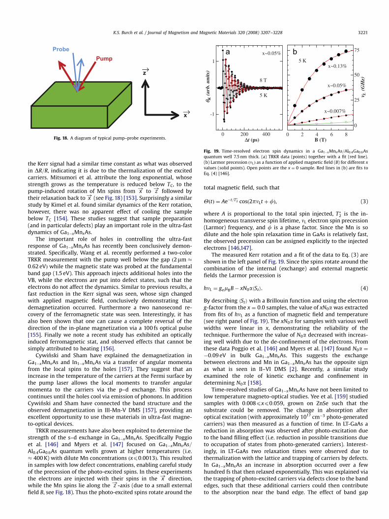
ARTICLE IN PRESS
ν L (
GH
z)
θ K (a
rb. u
nits
)
Δt (ps)
x~0.05%
8 T
5 K
5 Kx~0.13%
x~0.05%
x~0.007%
B (T)0
-1
1
75
50
25
0
86420400200
a b
Fig. 19. Time-resolved electron spin dynamics in a Ga1�xMnxAs=Al0:4Ga0:6As
quantum well 7.5 nm thick. (a) TRKR data (points) together with a fit (red line).
(b) Larmor precession ðnLÞ as a function of applied magnetic field (B) for different x
values (solid points). Open points are the x ¼ 0 sample. Red lines in (b) are fits to
Eq. (4) [146].
ProbePump
z
x
→
→
Fig. 18. A diagram of typical pump–probe experiments.
K.S. Burch et al. / Journal of Magnetism and Magnetic Materials 320 (2008) 3207–3228 3221
the Kerr signal had a similar time constant as what was observedin DR=R, indicating it is due to the thermalization of the excitedcarriers. Mitsumori et al. attribute the long exponential, whosestrength grows as the temperature is reduced below TC, to thepump-induced rotation of Mn spins from x
!to z!
followed bytheir relaxation back to x
!(see Fig. 18) [153]. Surprisingly a similar
study by Kimel et al. found similar dynamics of the Kerr rotation,however, there was no apparent effect of cooling the samplebelow TC [154]. These studies suggest that sample preparation(and in particular defects) play an important role in the ultra-fastdynamics of Ga1�xMnxAs.
The important role of holes in controlling the ultra-fastresponse of Ga1�xMnxAs has recently been conclusively demon-strated. Specifically, Wang et al. recently performed a two-colorTRKR measurement with the pump well below the gap ð2mm �0:62 eVÞ while the magnetic state was probed at the fundamentalband gap (1.5 eV). This approach injects additional holes into theVB, while the electrons are put into defect states, such that theelectrons do not affect the dynamics. Similar to previous results, afast reduction in the Kerr signal was seen, whose sign changedwith applied magnetic field, conclusively demonstrating thatdemagnetization occurred. Furthermore a two nanosecond re-covery of the ferromagnetic state was seen. Interestingly, it hasalso been shown that one can cause a complete reversal of thedirection of the in-plane magnetization via a 100 fs optical pulse[155]. Finally we note a recent study has exhibited an opticallyinduced ferromagnetic stat, and observed effects that cannot besimply attributed to heating [156].
Cywinski and Sham have explained the demagnetization inGa1�xMnxAs and In1�xMnxAs via a transfer of angular momentafrom the local spins to the holes [157]. They suggest that anincrease in the temperature of the carriers at the Fermi surface bythe pump laser allows the local moments to transfer angularmomenta to the carriers via the p–d exchange. This processcontinues until the holes cool via emission of phonons. In additionCywinski and Sham have connected the band structure and theobserved demagnetization in III-Mn-V DMS [157], providing anexcellent opportunity to use these materials in ultra-fast magne-to-optical devices.
TRKR measurements have also been exploited to determine thestrength of the s–d exchange in Ga1�xMnxAs. Specifically Poggioet al. [146] and Myers et al. [147] focused on Ga1�xMnxAs=Al0:4Ga0:6As quantum wells grown at higher temperatures (i.e.� 400 K) with dilute Mn concentrations ðxp0:0013Þ. This resultedin samples with low defect concentrations, enabling careful studyof the precession of the photo-excited spins. In these experimentsthe electrons are injected with their spins in the x
!direction,
while the Mn spins lie along the z!
-axis (due to a small externalfield B, see Fig. 18). Thus the photo-excited spins rotate around the
total magnetic field, such that
YðtÞ ¼ Ae�t=T�2 cosð2pnLt þfÞ, (3)
where A is proportional to the total spin injected, T�2 is the in-homogeneous transverse spin lifetime, nL electron spin precession(Larmor) frequency, and f is a phase factor. Since the Mn is sodilute and the hole spin relaxation time in GaAs is relatively fast,the observed precession can be assigned explicitly to the injectedelectrons [146,147].
The measured Kerr rotation and a fit of the data to Eq. (3) areshown in the left panel of Fig. 19. Since the spins rotate around thecombination of the internal (exchange) and external magneticfields the Larmor precession is
hnL ¼ gemBB� xN0ahSzi. (4)
By describing hSzi with a Brillouin function and using the electrong-factor from the x ¼ 0:0 samples, the value of xN0a was extractedfrom fits of hnL as a function of magnetic field and temperature(see right panel of Fig. 19). The xN0a for samples with various wellwidths were linear in x, demonstrating the reliability of thetechnique. Furthermore the value of N0a decreased with increas-ing well width due to the de-confinement of the electrons. Fromthese data Poggio et al. [146] and Myers et al. [147] found N0a ¼�0:09 eV in bulk Ga1�xMnxAs. This suggests the exchangebetween electrons and Mn in Ga1�xMnxAs has the opposite signas what is seen in II–VI DMS [2]. Recently, a similar studyexamined the role of kinetic exchange and confinement indetermining N0a [158].
Time-resolved studies of Ga1�xMnxAs have not been limited tolow temperature magneto-optical studies. Yee et al. [159] studiedsamples with 0:008pxp0:059, grown on ZnSe such that thesubstrate could be removed. The change in absorption afteroptical excitation (with approximately 1017 cm�3 photo-generatedcarriers) was then measured as a function of time. In LT-GaAs areduction in absorption was observed after photo-excitation dueto the band filling effect (i.e. reduction in possible transitions dueto occupation of states from photo-generated carriers). Interest-ingly, in LT-GaAs two relaxation times were observed due tothermalization with the lattice and trapping of carriers by defects.In Ga1�xMnxAs an increase in absorption occurred over a fewhundred fs that then relaxed exponentially. This was explained viathe trapping of photo-excited carriers via defects close to the bandedges, such that these additional carriers could then contributeto the absorption near the band edge. The effect of band gap
ARTICLE IN PRESS
K.S. Burch et al. / Journal of Magnetism and Magnetic Materials 320 (2008) 3207–32283222
re-normalization was also excluded since the increase in absorp-tion did not depend on the probe wavelength.
3.6. Origin of the states near the Fermi level in Ga1�xMnxAs
An essential issue for descriptions of the properties ofGa1�xMnxAs is whether the states at the Fermi energy in metallicsamples are best described in terms of VB holes of the GaAs hostor if these states preserve IB character. A resolution of the issue isneeded for the in-depth understanding of carrier mediatedferromagnetism in this prototypical III–V ferromagnet and alsofor assessment of its potential for spintronics device concepts. Inorder to resolve this issue, systematic transport and spectroscopicexperiments have been carried out by many research teamsworldwide and we believe emerging trends overviewed inSections 3.1–3.4 allow one to draw a number of firm conclusions.It should be noted that the nature of electronic transport inheavily disordered and compensated semiconductors is anextremely complicated problem even when all relevant impuritiesare non-magnetic [48,49,51,160]. While a cursory survey of theliterature on Ga1�xMnxAs may suggest strong disagreements inthe community on the IB versus VB controversy, a deeperinspection of published works uncovers emerging consensus onmany substantive matters.
First, it is uniformly agreed that the properties of Ga1�xMnxAsin the immediate vicinity of the MIT (i.e. x ’ 0:02) are bestunderstood within the IB scenario. Importantly, ferromagnetism isregistered on both the insulating and the metallic side of thetransition [161,162]. The survival of ferromagnetism in theinsulating samples clearly shows that band like transport of holesin the VB is not necessary to produce long-range spin order inthe system. Second, proponents of either of the two points ofview appear to agree on the fact that in metallic samples theVB states overlap with the IB states in the low doping regime[27,31,32,36,38,59,61,101,106,107,119,148,161,163–169]. In this re-gime, a canonical form of activated electronic transport is neitherexpected theoretically nor is it experimentally observed [49,51].At the same time many features of the dc transport and magneto-transport data in Ga1�xMnxAs point to deviations from the Fermiliquid picture of mobile holes in the VB. For example, the latterpicture is not consistent with a non-monotonic behavior of theresistivity both in the limit of the lowest T and in the vicinity ofthe Curie temperature [39,165,169–171].
The totality of spectroscopic data discussed in Sections 3.1–3.4support the view that the IB states preserve their identity derivedfrom the d-character of Mn dopants even in the regime in whichthese states overlap with the VB on the metallic side of themetal–insulator transition. Conventional wisdom of heavily dopedsemiconductors teaches us that on the metallic side of thetransition the IB and the host band merge into one inseparableband (see Section 1.2). It is worth pointing out that this picturehas been developed primarily for non-magnetic dopants and is atvariance with the rich physics of resonant states formed bymagnetic impurities in metals. Remarkable manifestations ofthese resonant impurity states include various anomalies of theresistivity as well as a dramatic enhancement of the effective massof mobile charges compared to the band structure values [172].Furthermore, the optical effective masses in Ga1�xMnxAs,inferred from the oscillator strength analysis of infrared data(see Section 3.1), yield m� on the order of 10 times me, [69,99,100]a result recently confirmed by studies of the mobility ofGa1�x�yMnxAsBey [203]. These high masses should be contrastedwith the value �0:38me determined from transport of holesintroduced by non-magnetic dopants into the VB [118]. The aboveexperiments and many additional findings reviewed in this paper
are therefore best described within the framework of the Mn-induced IB formed within the band gap of the GaAs host.
Holes in Ga1�xMnxAs uncover an intriguing dichotomy: finitevalues of the dc conductivity in the limit of T ! 0 unequivocallyestablish metallic transport due to extended states and yet otherproperties including a MIR resonance in the optical conductivitymeasurements are best understood in terms of transitionsinvolving the bound impurity states. In addition, the dc transportis quite exotic and is characterized by much lower mobility thanin In1�xMnxAs (see Refs. [86,99,169]) along with weak localizationeffects [171]. Ohno and Dietl [173] have discussed this ratherexotic character of III-Mn-V systems in the context of the so-called‘‘two-fluid model’’ of transport in conventional disorderedsemiconductors intended to reconcile the coexistence of band-like and impurity-like properties [160]. While such a model is anintriguing possibility, its realization requires nearly phase sepa-rated character of the studied materials near the MIT boundary.Furthermore, the materials should become more homogeneous asthe carrier density is increased (as the samples become moremetallic). Nonetheless the experimental findings reported heresuggest the electronic behavior of samples with the highest TC
values reported to date are best understood in the IB scenario. Inaddition, no local probes have uncovered such effects inGa1�xMnxAs [105,163,174–178]. We therefore believe that holesat the Fermi energy in ferromagnetic and metallic Ga1�xMnxAs arelikely to be described by the IB scenario. Nonetheless, furtheroptical experiments in samples where the disorder, Mn andcarrier densities are independently tuned would help to solve thiscontroversy.
4. Ga1�xMnxP
TMs in GaP have been the subject of extensive studies thatexamined the evolution of the electronic structure with differentTM (see Ref. [23] and references therein). Interestingly in diluteGa1�xMnxP the Lyman series corresponding to acceptors bound tothe Mn have a large binding energy (400 meV) [23,179]. Thissuggests the Mn acceptor state is both unconventional and that ametallic state will be exceedingly difficult to produce. In fact,there have been no reports of a metallic state in Ga1�xMnxP.Nonetheless, due to its close lattice matching with Si, Ga1�xMnxPmay turn out to be a particularly fruitful avenue for incorporatingDMS in well established semiconductor technologies [180]. Earlyreports of growth by MBE and ion-implantation [181] suggested amagnetic state in Ga1�xMnxP with a TC exceeding room tempera-ture, however, these reports remain unconfirmed and did notestablish the nature of the carriers mediating the ferromagneticstate. Recently Ga1�xMnxP has been prepared by ion-implantationwith a maximum x � 0:06 and TC � 60 K. This study found thatthe samples were always insulating and that the Curie tempera-ture was reduced by co-doping with the donor Te [182].
In order to establish the nature of the bound holes inGa1�xMnxP, Scarpulla et al. performed optical absorption andphotoconductivity measurements [182]. The absorption spectra ofa Ga0:94Mn0:06P:Te sample is shown in Fig. 20, where a peak isobserved centered near 400 meV, the location of the Mn impuritylevel. The absence of other spectral features suggests the Fermilevel is in the Mn IB and has not crossed into the GaP VB. Tofurther confirm that the holes reside in the Mn-induced IB, theauthors measured the dc conductivity induced by optical excita-tion at low temperatures. In Fig. 20 this photoconductivityspectrum for the Ga0:94Mn0:06P sample is displayed along withthe spectrum for the incident light. The onset for the photo-conductivity data is clearly higher in energy than the incidentlight, indicating the holes reside in bound states that are

ARTICLE IN PRESS
200A
bsor
banc
e (a
.u.)
Energy (meV)0
Phot
ocon
duct
ivity
(a.u
.)
Energy (meV)600500400300125100755025
Fig. 20. Left panel: (dashed line) incident intensity (red lines) photoconductivity
of a Ga1�xMnxP sample. Right panel: 10 K absorption spectra of Ga1�xMnxP sample
compensated with Te. Sharp features in the absorption are due to GaP phonon
features [182].
K.S. Burch et al. / Journal of Magnetism and Magnetic Materials 320 (2008) 3207–3228 3223
separated by roughly � 26 meV from the conducting states in theVB. This value corresponds well with the size of the gapdetermined from the thermal activation energy of the resistivity(31 meV). By co-doping with the donor Te, the Fermi energy wasmoved deeper into the Mn-induced IB and the gap increased[182]. Lastly, the size of the gap between the Fermi energy andextended states ð26 meV � 300 KÞ indicates that localized holesmediate the ferromagnetism.
0.5102
103
104
105
ρESR~ 2x 1018cm-3
Ab
sorp
tio
n c
oef
fici
ent
(cm
-1)
Photon Energy (eV)
GaN:Mn (Mn3+)
ρESR~ 3x 1019cm-3GaN:Mn:Si (Mn2+)
3.53.02.52.01.51.0
Fig. 21. Optical absorption of Ga1�xMnxN samples before and after Si co-doping.
Only the Ga1�xMnxN sample reveals features at 1.5 eV and above 1.8 eV, indicating
EF is above the Mn d-levels in Ga1�xMnxN:Si [185].
5. Ga1�xMnxN
For the last decade there has been growing interest in wideband gap, group III-nitrides, for their potential use in high power/temperature electronics, solar-blind UV detectors and blue/green/UV light emitting diodes [180]. In addition, Dietl et al. suggestedGa1�xMnxN should posses a TC well exceeding room temperaturebased upon a mean field model of ferromagnetism in DMS [98].This has led to a flurry of research on Ga1�xMnxN resulting in itsgrowth by multiple methods including plasma assisted MBE[183–186], MOVPE [187,188], nebulized spray pyrolysis [189], ion-implantation [190], the ammonothermal method [191,192], andbulk crystals grown by the high pressure technique [193]. In manyof these reports ferromagnetic behavior has been claimed to existat or above room temperature along with the correspondingsignatures of a carrier mediated magnetic state, such as theanomalous Hall effect [180]. However, others have either reportedferromagnetism at only very low temperatures [183] or haveprovided evidence that the high TC ferromagnetism originatesfrom clusters [190,192,194,195]. Therefore it is not surprising thatto date there is no consensus on whether ferromagnetism inGa1�xMnxN is intrinsic or due to a secondary phase in the GaNhost. Nonetheless, a consensus has emerged regarding the effectsof the Mn dopant on the GaN band structure. Therefore ourdiscussion will focus on studies elucidating the changes in theGaN band structure due to the Mn impurity.
Before discussing the optical properties, we address a keymaterials growth issue that has emerged in the course of attemptsto produce ferromagnetic Ga1�xMnxN. Due to the lack ofcommercially available GaN substrates, Ga1�xMnxN is often grownon lattice mismatched substrates (e.g. SiC, Si, and sapphire). Whilethis is advantageous for the incorporation of GaN-based devicesinto standard electronics, it also results in a large dislocationdensity. Therefore as-grown GaN generally has a very highnumber of charged defects resulting in a very high electrondensity [180]. As a result, Ga1�xMnxN is usually found to be n-typeand must be co-doped with Mg to be made p-type.
5.1. Absorption spectra of Ga1�xMnxN
Some of the earliest data indicating that Mn formed a deepacceptor level in Ga1�xMnxN were optical absorption spectra[74,187,188]. A typical spectrum is shown in Fig. 21, where twoprominent features are observed, one centered at 1.5 eV and theother with an onset around 2.0 eV. From these spectra it wasinitially believed that Mn produced an acceptor level approxi-mately 1.4 eV above the VB of Ga1�xMnxN. Specifically, the lowerenergy peak was assigned to optical transitions of electrons fromthe VB to the Mn acceptor level. The higher energy resonance wasthen assigned to transitions from the acceptor level to theGa1�xMnxN conduction band [187,188,196]. Support for the notionthat the holes in Ga1�xMnxN do not reside in the VB was alsoprovided by an extensive study of the band gap. In particular itwas shown that the small changes in the band gap could beattributed to structural changes from the Mn and not theMoss–Burstein effect [197].
It was quickly realized that the original assignment of the1.4 and 2.0 eV features did not explain the wealth of data thatemerged. In particular, if the assignment was correct, one mightexpect that adding electrons to the system would fill the Mn IB,such that the lower energy transition (from the VB), would nolonger be possible. At the same time one would also expect thatadding donors to the system would also result in an increase inthe spectral weight of the higher energy transition. However, itwas soon shown that co-doping Ga1�xMnxN with Si (i.e. addingelectrons) resulted in a removal of spectral weight from bothfeatures (see Fig. 21) [185]. Furthermore, spectra taken at lowtemperatures revealed a significant sharpening of the lowerenergy feature and not the higher energy resonance. In fact, atlow temperatures one can resolve phonon-replicas of the lowerenergy resonance (i.e. resonances that involve the main transitionplus the emission of an optical phonon). This indicates that thetwo features have significantly different origins.
An alternate interpretation of the data soon emerged. Namelythat the Mn d-levels lie in the gap of GaN with the upper most EG
level approximately 2.1 eV above the VB. Therefore the 2.0 eVfeature results from transitions between the VB and the Mn 5Elevel, while the lower energy absorption was attributed to internalMn transitions between the 5T2 and 5E levels [185,195]. Such anassignment helps to explain a number of the results describedabove. Specifically, the sharpness of the low energy feature results

ARTICLE IN PRESS
0.5
1.0
1.5
2.0
320Magnetic field [mT]
EP
R a
mp
litu
de
No
rmal
ized
EP
R a
mp
litu
de
[arb
un
its]
Illumination energy (eV)
GaN:Mn,Mg
T=6KB || c, X-band
dark Mn2+ resonance illumination with
2.0-3.5eV light
3.02.52.01.51.0
360340
Fig. 22. Inset: EPR spectra of Mn2þ (d5) Ga1�xMnxN before (dashed lines) and after
(solid lines) illumination at 2.0 eV. Main panel: strength of the EPR ðd5Þ signal as a
function of illumination energy, indicating the charge state of the Mn only changes
for light greater than 2.0 eV [193].
K.S. Burch et al. / Journal of Magnetism and Magnetic Materials 320 (2008) 3207–32283224
from the fact that it involves transitions between two narrowbands with much smaller bandwidth than the valence orconduction bands. This scenario also explains the evolution ofboth resonances upon adding electrons to the system. Electronparamagnetic resonance (EPR) experiments have also helped toresolve the origin of these features. Specifically, EPR experimentsrevealed that the Mn-induced absorption features were onlyobserved in samples wherein the Mn was in a 3+ charge state(i.e. d4) and disappeared in samples where the Mn was in a2þ (i.e. d5) configuration [185,195]. Additionally, an increase inthe EPR signal of the Mn2þ
ðd5Þ was observed when the samples
were illuminated with light [193]. However, as shown in Fig. 22,this effect only occurred for light with energies above 2.0 eV,indicating that the absorption at lower energies did not involve achange in the charge state of the Mn. Therefore the EPR resultsconfirm the assertion that the optical absorption observed below2.0 eV only involves transitions on the Mn atom. Whereas forabsorption above 2.0 eV, the transitions result in an increase in thenumber of electrons on the Mn atom, which is consistent with atransition from the VB to the Mn d-level.
Fig. 23. Center energy of absorption features in a Ga0:97Mn0:03N layer as a function
of the magnetic field in Faraday and the Voigt configurations. The symbol size is
proportional to the intensity of the feature [198].
5.2. Magneto-optics of Ga1�xMnxN
A number of groups have studied the magneto-opticalresponse of Ga1�xMnxN using a variety of techniques. The earlieststudies of the MCD of Ga1�xMnxN were done by Ando [194]wherein no ferromagnetic component was observed. This stronglysuggested that the room temperature ferromagnetism is not anintrinsic property of the Ga1�xMnxN samples studied. Later, workby Ferrand et al. did register an MCD signal from which theyextracted a Zeeman splitting that was proportional to themagnetization at low temperatures. They were therefore able toextract a measure of the exchange constants: N0ða� bÞ ¼ 0:2 eV[184]. While this value is low, one should note that the MCDfeatures were quite broad, and at the band gap two features wereoverlapped. Nonetheless, the fact that the low temperature MCDsignal was observed at the fundamental band gap of GaN indicatesthat the low temperature ferromagnetism is indeed intrinsic andnot due to the formation of second phase [47].
In addition to the MCD work mentioned above, two groupshave also measured the change in absorption with appliedmagnetic field. The first such study by Wolos et al. focused on
the effects of magnetic field on the 1.4 eV feature, where smallshifts in the zero-phonon line (ZPL) were seen with appliedmagnetic field. However, at 7 T a sudden jump occurred, afterwhich a gradual shift of the peak continued. Interestingly littleeffect of magnetic field was observed in the Voight configuration.This behavior is completely at odds with what one would expect ifthe transition originated in the VB, providing further evidencethat the 1.4 eV feature results from Mn d to d transitions. Toconfirm this assignment Wolos et al. solved a model for the Mnlevels that accounted for crystal field splitting, a static Jahn–Tellerdistortion, the trigonal crystal field, the spin–orbit interaction andthe Zeeman splitting of the levels [199]. In this model oneassumes that the ZPL results from transitions between 5T2 and 5Estates. From spin–orbit coupling, the states can then be labeledwith magnetic numbers ms ¼ 2;1;0;�1;2, the energies of whichwill have different field dependencies. Therefore the calculationsuggests that at small fields the shifts seen in the absorptionare primarily due to the Zeeman effect. However, at larger fieldstwo of the levels cross, leading to a jump in the energy of theresonance [199].
The hypothesis of the dominant role of internal Mn transitionswas later confirmed by Marcet et al., who studied the magneto-optical absorption at much lower dopings, such that the disorderwas minimized [198]. From their spectra, one clearly observesthree peaks in the absorption that only exist at certain magneticfield values and orientations. The different peak positions areshown in Fig. 23, indicating that the apparent jump in the spectraobserved in the earlier study [199] is due to a shift in spectralweight from the L1 to L2 transitions. In Fig. 24 we show therelevant energy level scheme as calculated by Marcet et al. thatexplains the origin of the three transitions and their fielddependence [198].
5.3. Luminescence of Ga1�xMnxN
As described above luminescence studies can be quite power-ful due to their ability to investigate defect levels and the well-defined selection rules involved in the emission of light. We firstfocus on the mid-gap PL, performed by Korotkov et al., whereinregardless of the excitation wavelength a feature with a number ofreplicas was seen around 1.0 eV [187,188]. Interestingly thisfeature also appeared to be rather long-lived (i.e. exponentialdecay with characteristic time: t � 75ms). It has been shown thatin as-grown Ga1�xMnxN a strong, albeit broad emission was seen
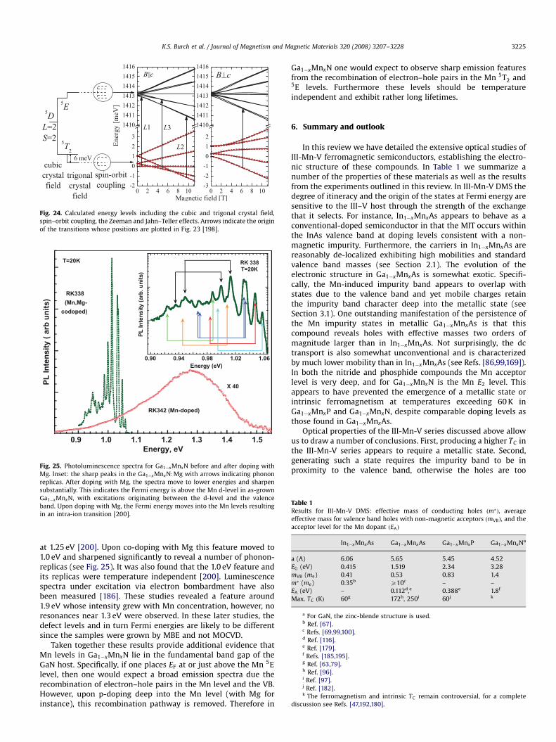
ARTICLE IN PRESS
Table 1Results for III-Mn-V DMS: effective mass of conducting holes ðm�Þ, average
effective mass for valence band holes with non-magnetic acceptors ðmVBÞ, and the
acceptor level for the Mn dopant ðEAÞ
In1�xMnxAs Ga1�xMnxAs Ga1�xMnxP Ga1�xMnxNa
a (A) 6.06 5.65 5.45 4.52
EG (eV) 0.415 1.519 2.34 3.28
mVB (me) 0.41 0.53 0.83 1.4
m� (me) 0.35bX10c – –
EA (eV) – 0.112d,e 0.388e 1.8f
Max. TC ðKÞ 60g 172h, 250i 60j k
a For GaN, the zinc-blende structure is used.b Ref. [67].c Refs. [69,99,100].d Ref. [116].e Ref. [179].f Refs. [185,195].g Ref. [63,79].h Ref. [96].i Ref. [97].j Ref. [182].k The ferromagnetism and intrinsic TC remain controversial, for a complete
discussion see Refs. [47,192,180].
0.9
PL In
tens
ity (
arb
units
)
Energy, eV
RK342 (Mn-doped)
RK338 (Mn,Mg-
codoped)
X 40
T=20K
0.90
PL In
tens
ity (a
rb. u
nits
)
Energy (eV)
RK 338T=20K
1.51.41.31.21.11.0
1.061.020.980.94
Fig. 25. Photoluminescence spectra for Ga1�xMnxN before and after doping with
Mg. Inset: the sharp peaks in the Ga1�xMnxN:Mg with arrows indicating phonon
replicas. After doping with Mg, the spectra move to lower energies and sharpen
substantially. This indicates the Fermi energy is above the Mn d-level in as-grown
Ga1�xMnxN, with excitations originating between the d-level and the valence
band. Upon doping with Mg, the Fermi energy moves into the Mn levels resulting
in an intra-ion transition [200].
g
Fig. 24. Calculated energy levels including the cubic and trigonal crystal field,
spin–orbit coupling, the Zeeman and Jahn–Teller effects. Arrows indicate the origin
of the transitions whose positions are plotted in Fig. 23 [198].
K.S. Burch et al. / Journal of Magnetism and Magnetic Materials 320 (2008) 3207–3228 3225
at 1.25 eV [200]. Upon co-doping with Mg this feature moved to1.0 eV and sharpened significantly to reveal a number of phonon-replicas (see Fig. 25). It was also found that the 1.0 eV feature andits replicas were temperature independent [200]. Luminescencespectra under excitation via electron bombardment have alsobeen measured [186]. These studies revealed a feature around1.9 eV whose intensity grew with Mn concentration, however, noresonances near 1.3 eV were observed. In these later studies, thedefect levels and in turn Fermi energies are likely to be differentsince the samples were grown by MBE and not MOCVD.
Taken together these results provide additional evidence thatMn levels in Ga1�xMnxN lie in the fundamental band gap of theGaN host. Specifically, if one places EF at or just above the Mn 5Elevel, then one would expect a broad emission spectra due therecombination of electron–hole pairs in the Mn level and the VB.However, upon p-doping deep into the Mn level (with Mg forinstance), this recombination pathway is removed. Therefore in
Ga1�xMnxN one would expect to observe sharp emission featuresfrom the recombination of electron–hole pairs in the Mn 5T2 and5E levels. Furthermore these levels should be temperatureindependent and exhibit rather long lifetimes.
6. Summary and outlook
In this review we have detailed the extensive optical studies ofIII-Mn-V ferromagnetic semiconductors, establishing the electro-nic structure of these compounds. In Table 1 we summarize anumber of the properties of these materials as well as the resultsfrom the experiments outlined in this review. In III-Mn-V DMS thedegree of itineracy and the origin of the states at Fermi energy aresensitive to the III–V host through the strength of the exchangethat it selects. For instance, In1�xMnxAs appears to behave as aconventional-doped semiconductor in that the MIT occurs withinthe InAs valence band at doping levels consistent with a non-magnetic impurity. Furthermore, the carriers in In1�xMnxAs arereasonably de-localized exhibiting high mobilities and standardvalence band masses (see Section 2.1). The evolution of theelectronic structure in Ga1�xMnxAs is somewhat exotic. Specifi-cally, the Mn-induced impurity band appears to overlap withstates due to the valence band and yet mobile charges retainthe impurity band character deep into the metallic state (seeSection 3.1). One outstanding manifestation of the persistence ofthe Mn impurity states in metallic Ga1�xMnxAs is that thiscompound reveals holes with effective masses two orders ofmagnitude larger than in In1�xMnxAs. Not surprisingly, the dctransport is also somewhat unconventional and is characterizedby much lower mobility than in In1�xMnxAs (see Refs. [86,99,169]).In both the nitride and phosphide compounds the Mn acceptorlevel is very deep, and for Ga1�xMnxN is the Mn E2 level. Thisappears to have prevented the emergence of a metallic state orintrinsic ferromagnetism at temperatures exceeding 60 K inGa1�xMnxP and Ga1�xMnxN, despite comparable doping levels asthose found in Ga1�xMnxAs.
Optical properties of the III-Mn-V series discussed above allowus to draw a number of conclusions. First, producing a higher TC inthe III-Mn-V series appears to require a metallic state. Second,generating such a state requires the impurity band to be inproximity to the valence band, otherwise the holes are too

ARTICLE IN PRESS
0.002
0.00
0.25
0.50
0.75
1.00
1.25
1.50
1.75
2.00
InAs
InPGaAs
AlAsGaP
GaN
E A (e
V)
1/a(7/2) (Angstroms-7/2)
InsulatorMetal
0.0050.0040.003
Fig. 26. Acceptor level for dilute Mn in III–V compounds ðEAÞ versus the inverse
lattice spacing ð1=a7=2Þ. As the hybridization between d and p-orbitals is increased,
approximated via 1=a7=2, the impurity level moves deeper into the band gap,
reducing the likelihood of a metallic state. Data taken from Ref. [202] and those
indicated in Table 1.
K.S. Burch et al. / Journal of Magnetism and Magnetic Materials 320 (2008) 3207–32283226
strongly localized around the Mn. As suggested theoretically[36,57,59,168], this separation is effected by the strength of thehybridization between Mn d electrons and the p-orbitalsof its neighbors, an assertion recently confirmed by studies ofGaMnBeAs and GaMnAsP [203]. This indicates that this keyparameter can be tuned by choosing the appropriate III–V host, aquite novel aspect of these compounds. Indeed, from a simpletight-binding picture, one would expect the hybridization to beinversely proportional to the lattice constant (i.e. Vpd / 1=a7=2)[201]. To explore this possibility in Fig. 26 we plot the acceptorlevel in the dilute limit versus 1=a7=2 for various III–V hosts. Asshown in the figure, not only is the electronic structure effected bythe strength of Vpd, as measured by the lattice constant, but thisimportant parameter also controls the degree of itineracy of theholes.
Before concluding we would like to make some remarks on thefuture of this exciting field. The studies outlined here clearlydemonstrate a strong connection between the magnetism andoptical properties of III-Mn-V semiconductors. They also establisha unique role for the III–V host in combination with a TM dopant.Specifically, the trends established here for III-Mn-V DMS could beemployed to engineer a desired combination of magnetic,transport and optical properties. Furthermore, a number ofavailable controls including light illumination, electric and/magnetic fields enable manipulation of the interplay betweenthe properties of III-Mn-V semiconductors. Nonetheless the widearray of potential magneto-optical devices these compoundstherefore offer, still remains to be fully exploited.
In addition to the applications of III-Mn-V yet to beimplemented, there are also a number of open scientific questionsthat need to be studied. First and foremost, the nature andstrength of the exchange constants in the phosphorus andnitrogen based III-Mn-V semiconductors should be established.Second, a detailed mapping of the broad band (i.e. far and mid-infrared) magneto-optical response of these compounds mayproduce useful insights into the nature of the states in the As andP based III-Mn-V DMS, as well as produce magneto-optical devicesin this range. Lastly, a realistic picture of the MIT in III-Mn-V DMSwould help reveal the connections between their magnetic andelectronic properties.
Acknowledgments
We are grateful for numerous discussions with K. Alberi,O.D. Dubon, M.E. Flatte, J.K. Furdyna, B. Lee, X. Liu, A. MacDonald,A.J. Millis, S. Das Sarma, M.A. Scarpulla, J. Sinova, J.-M. Tang, andC. Timm. We are especially en-debited to S. Crooker, L. Cywinski,M.P. Kennett, and E.J. Singley for careful reading of this manu-script. K.S.B. acknowledges support from the Los Alamos NationalLaboratory LDRD and the Center for Integrated Nanotechnologies.D.N.B. appreciates support from ONR Award N00014-07-1-347.
References
[1] J. Schneider, Defects in Semiconductors II, North-Holland, New York, 1983,p. 225.
[2] J.K. Furdyna, J. Appl. Phys. 64 (4) (1988) R29.[3] T. Dietl, Sem. Sci. Tech. 17 (4) (2002) 377.[4] A.H. MacDonald, P. Schiffer, N. Samarth, Nat. Mater. 4 (2005) 195.[5] H. Ohno, J. Magn. Magn. Mater. 200 (1–3) (1999) 110.[6] B. Clerjaud, J. Phys. C 18 (19) (1985) 3615.[7] T. Jungwirth, J. Sinova, J. Masek, J. Kucera, A.H. MacDonald, Rev. Mod. Phys.
78 (3) (2006) 809.[8] S.A. Wolf, D.D. Awschalom, R.A. Buhrman, J.M. Daughton, S. von Molnar,
M.L. Roukes, A.Y. Chtchelkanova, D.M. Treger, Science 294 (5546) (2001) 1488.[9] I. Zutic, J. Fabian, S. Das Sarma, Rev. Mod. Phys. 76 (2) (2004) 323.
[10] D.D. Awschalom, M.E. Flatte, Nat. Phys. 3 (3) (2007) 153.[11] E. Grochowski, R. Halem, IBM Syst. J. 42 (2) (2003) 338.[12] C.P. Weber, N. Gedik, J.E. Moore, J. Orenstein, J. Stephens, D.D. Awschalom,
Nature 437 (7063) (2005) 1330.[13] J. Stephens, J. Berezovsky, J.P. McGuire, L.J. Sham, A.C. Gossard, D.D. Awschalom,
Phys. Rev. Lett. 93 (9) (2004) 097602.[14] J.M. Kikkawa, J.A. Gupta, I. Malajovich, D.D. Awschalom, Physica E 9 (1)
(2001) 194.[15] G. Salis, Y. Kato, K. Ensslin, D.C. Driscoll, A.C. Gossard, D.D. Awschalom,
Nature 414 (6864) (2001) 619.[16] Y.K. Kato, R.C. Myers, A.C. Gossard, D.D. Awschalom, Science 306 (5703)
(2004) 1910.[17] S.A. Crooker, M. Furis, X. Lou, C. Adelmann, D. Smith, C.J. Palmstrom,
P. Crowell, Science 309 (5744) (2005) 2191.[18] J. Zak, E.R. Moog, C. Liu, S.D. Bader, J. Magn. Magn. Mater. 89 (1–2) (1990)
107.[19] S.V. Kravchenko, M.P. Sarachik, Rep. Prog. Phys. 67 (1) (2004) 1.[20] F.D.M. Haldane, P.W. Anderson, Phys. Rev. B 13 (6) (1976) 2553.[21] N. Brandt, V. Moshchalkov, Adv. Phys. 33 (1984) 193.[22] T. Dietl, Handbook on Semiconductors, vol. 3b, North-Holland, Amsterdam,
1994, p. 1327 (Chapter 17).[23] V. Singh, A. Zunger, Phys. Rev. B 31 (6) (1985) 3729.[24] H. Munekata, H. Ohno, S. von Molnar, A. Segmuller, L.L. Chang, L. Esaki, Phys.
Rev. Lett. 63 (17) (1989) 1849.[25] H. Ohno, A. Shen, F. Matsukura, A. Oiwa, A. Endo, S. Katsumoto, Y. Iye, Appl.
Phys. Lett. 69 (3) (1996) 363.[26] C. Timm, J. Phys. Condens. Matter 15 (50) (2003) R1865.[27] P. Mahadevan, A. Zunger, Phys. Rev. B 69 (11) (2004) 115211.[28] Y. Zhang, S. Das Sarma, Phys. Rev. B 72 (12) (2005) 125303.[29] S. Picozzi, A. Continenza, M. Kim, A.J. Freeman, Phys. Rev. B 73 (23) (2006)
235207.[30] G.D. Sanders, Y. Sun, F.V. Kyrychenko, C.J. Stanton, G.A. Khodaparast,
M.A. Zudov, J. Kono, Y.H. Matsuda, N. Miura, H. Munekata, Phys. Rev. B 68(16) (2003) 165205.
[31] G. Alvarez, E. Dagotto, Phys. Rev. B 68 (4) (2003) 045202.[32] S. Sanvito, P. Ordejon, N.A. Hill, Phys. Rev. B 63 (16) (2001) 165206.[33] J. Fernandez-Rossier, C. Piermarocchi, P. Chen, A.H. MacDonald, L.J. Sham,
Phys. Rev. Lett. 93 (12) (2004) 127201.[34] B. Lee, X. Cartoixa, N. Trivedi, R.M. Martin, Disorder enhanced spin
polarization in diluted magnetic semiconductors, cond-mat/0702567.[35] C. Zhou, M.P. Kennett, X. Wan, M. Berciu, R.N. Bhatt, Phys. Rev. B (Condens.
Matter Mater. Phys.) 69 (14) (2004) 144419.[36] M.A. Majidi, J. Moreno, M. Jarrell, R.S. Fishman, K. Aryanpour, Phys. Rev. B 74
(11) (2006) 115205.[37] J.-M. Tang, M.E. Flatte, Phys. Rev. Lett. 92 (4) (2004) 047201.[38] G.A. Fiete, G. Zarand, K. Damle, C. Pascu Moca, Phys. Rev. B (Condens. Matter
Mater. Phys.) 72 (4) (2005) 045212.[39] E.H. Hwang, S. Das Sarma, Phys. Rev. B (Condens. Matter Mater. Phys.) 72 (3)
(2005) 035210.[40] P. Yu, M. Cardona, Fundamentals of Semiconductors, Springer, Berlin, 1996.[41] D.N. Basov, T. Timusk, Rev. Mod. Phys. 77 (2) (2005) 721.[42] L. Degiorgi, Rev. Mod. Phys. 71 (3) (1999) 687.[43] Y. Okimoto, Y. Tokura, J. Superconductivity 13 (2000) 271–284.[44] M. Imada, A. Fujimori, Y. Tokura, Rev. Mod. Phys. 70 (4) (1998) 1039.[45] S. Dordevic, D. Basov, Ann. Phys. 15 (7–8) (2006) 545.[46] K. Ando, K. Takahashi, T. Okuda, M. Umehara, Phys. Rev. B 46 (1992) 12289.
ARTICLE IN PRESS
K.S. Burch et al. / Journal of Magnetism and Magnetic Materials 320 (2008) 3207–3228 3227
[47] K. Ando, Science 312 (5782) (2006) 1883.[48] N. Mott, E. Davis, Electronic Processes in Non-Crystalline Materials,
Clarendon Press, Oxford, 1979.[49] A.L. Efros, B.I. Shklovskiı, Electronic Properties of Doped Semiconductors,
Springer Series in Solid-State Sciences, Springer, Berlin, 1984.[50] P.A. Lee, T.V. Ramakrishnan, Rev. Mod. Phys. 57 (2) (1985) 287.[51] R.F. Milligan, G.A. Thomas, Annu. Rev. Phys. Chem. 36 (1985) 139.[52] N. Mott, Can. J. Phys. 34 (12A) (1956) 1356.[53] S. Liu, K. Karrai, F. Dunmore, H.D. Drew, R. Wilson, G.A. Thomas, Phys. Rev. B
48 (15) (1993) 11394.[54] P. Coleman, AIP Conf. Proc. (629) (2002) 79.[55] P.W. Anderson, Phys. Rev. 109 (5) (1958) 1492.[56] B.E. Larson, K.C. Hass, H. Ehrenreich, A.E. Carlsson, Phys. Rev. B 37 (8) (1988)
4137.[57] A.K. Bhattacharjee, C.B.A. la Guillaume, Solid State Commun. 113 (1)
(1999) 17.[58] M. Berciu, R.N. Bhatt, Phys. Rev. B 69 (4) (2004) 045202.[59] A. Chattopadhyay, S. Das Sarma, A.J. Millis, Phys. Rev. Lett. 87 (22) (2001)
227202.[60] S.C. Erwin, A.G. Petukhov, Phys. Rev. Lett. 89 (22) (2002) 227201.[61] O. Rader, C. Pampuch, A.M. Shikin, W. Gudat, J. Okabayashi, T. Mizokawa,
A. Fujimori, T. Hayashi, M. Tanaka, A. Tanaka, A. Kimura, Phys. Rev. B 69 (7)(2004) 075202.
[62] H. Ohno, H. Munekata, T. Penney, S. von Molnar, L.L. Chang, Phys. Rev. Lett.68 (17) (1992) 2664.
[63] H. Ohno, J. Crystal Growth 251 (1–4) (2003) 285.[64] T. Schallenberg, H. Munekata, Appl. Phys. Lett. 89 (2006) 042507.[65] G. Dresselhaus, A.F. Kip, C. Kittel, Phys. Rev. 98 (2) (1955) 368.[66] M.A. Zudov, J. Kono, Y.H. Matsuda, T. Ikaida, N. Miura, H. Munekata,
G.D. Sanders, Y. Sun, C.J. Stanton, Phys. Rev. B 66 (16) (2002) 161307.[67] Y.H. Matsuda, G.A. Khodaparast, M.A. Zudov, J. Kono, Y. Sun, F.V. Kyrychenko,
G.D. Sanders, C.J. Stanton, N. Miura, S. Ikeda, Y. Hashimoto, S. Katsumoto,H. Munekata, Phys. Rev. B 70 (19) (2004) 195211.
[68] K. Hirakawa, A. Oiwa, H. Munekata, Phys. E Low-dimensional Syst.Nanostructures 10 (1–3) (2001) 215.
[69] E.J. Singley, K.S. Burch, R. Kawakami, J. Stephens, D.D. Awschalom, D.N. Basov,Phys. Rev. B 68 (16) (2003) 165204.
[70] K. Lee, A.J. Heeger, Y. Cao, Phys. Rev. B 48 (20) (1993) 14884.[71] D.N. Basov, A.V. Puchkov, R.A. Hughes, T. Strach, J. Preston, T. Timusk,
D.A. Bonn, R. Liang, W.N. Hardy, Phys. Rev. B 49 (17) (1994) 12165.[72] M. Dumm, S. Komiya, Y. Ando, D.N. Basov, Phys. Rev. Lett. 91 (7) (2003)
077004.[73] S.-R.E. Yang, J. Sinova, T. Jungwirth, Y.P. Shim, A.H. MacDonald, Phys. Rev. B
67 (4) (2003) 045205.[74] S.S.A. Seo, M.W. Kim, Y.S. Lee, T.W. Noh, Y.D. Park, G.T. Thaler, M.E. Overberg,
C.R. Abernathy, S.J. Pearton, Appl. Phys. Lett. 82 (26) (2003) 4749.[75] A.J. Taylor, R.D. Averitt, J. Demsar, A.I. Lobad, J.L. Sarrao, S.A. Trugman,
Physica B Condens. Matter 312–313 (2002) 640.[76] R.H.M. Groeneveld, R. Sprik, A. Lagendijk, Phys. Rev. B 51 (17) (1995) 11433.[77] N. Bloembergen, Rev. Mod. Phys. 71 (2) (1999) S283.[78] D. Young, J. Gupta, E. Johnston-Halperin, R. Epstein, Y. Kato, D. Awschalom,
Semiconductor Sci. Technol. 17 (4) (2002) 275.[79] J. Wang, C. Sun, Y. Hashimoto, J. Kono, G.A. Khodaparast, L. Cywinski,
L.J. Sham, G.D. Sanders, C.J. Stanton, H. Munekata, J. Phys. Condens. Matter 18(31) (2006) R501.
[80] S. Koshihara, A. Oiwa, M. Hirasawa, S. Katsumoto, Y. Iye, C. Urano, H. Takagi,H. Munekata, Phys. Rev. Lett. 78 (24) (1997) 4617.
[81] X. Liu, W.L. Lim, L.V. Titova, T. Wojtowicz, M. Kutrowski, K.J. Yee,M. Dobrowolska, J.K. Furdyna, S.J. Potashnik, M.B. Stone, P. Schiffer,I. Vurgaftman, J.R. Meyer, Phys. E Low-dimensional Syst. Nanostructures20 (3–4) (2004) 370.
[82] A. Oiwa, T.S. Upinski, H. Munekata, Appl. Phys. Lett. 78 (4) (2001) 518.[83] H. Ohno, D. Chiba, F. Matsukura, T. Omiya, T. Dietl, Y. Ohno, K. Ontani, Nature
408 (2000) 944.[84] D. Chiba, M. Yamanouchi, F. Matsukura, H. Ohno, Science 301 (2003) 943.[85] R.C. Myers, B.L. Sheu, A.W. Jackson, A.C. Gossard, P. Schiffer, N. Samarth, D.D.
Awschalom, Phys. Rev. B (Condens. Matter Mater. Phys.) 74 (15) (2006)155203.
[86] Y. Iye, A. Oiwa, A. Endo, S. Katsumoto, F. Matsukura, A. Shen, H. Ohno,H. Munekata, Mater. Sci. Eng. B 63 (1–2) (1999) 88.
[87] K.W. Edmonds, P. Boguslawski, K.Y. Wang, R.P. Campion, S.N. Novikov,N.R.S. Farley, B.L. Gallagher, C.T. Foxon, M. Sawicki, T. Dietl, M. BuongiornoNardelli, J. Bernholc, Phys. Rev. Lett. 92 (3) (2004) 037201.
[88] K.M. Yu, W. Walukiewicz, T. Wojtowicz, I. Kuryliszyn, X. Liu, Y. Sasaki,J.K. Furdyna, Phys. Rev. B 65 (20) (2002) 201303.
[89] K.W. Edmonds, K.Y. Wang, R.P. Campion, A.C. Neumann, C.T. Foxon,B.L. Gallagher, P.C. Main, Appl. Phys. Lett. 81 (16) (2002) 3010.
[90] T. Hayashi, Y. Hashimoto, S. Katsumoto, Y. Iye, Appl. Phys. Lett. 78 (12) (2001)1691.
[91] S.J. Potashnik, K.C. Ku, S.H. Chun, J.J. Berry, N. Samarth, P. Schiffer, Appl. Phys.Lett. 79 (10) (2001) 1495.
[92] M.B. Stone, K.C. Ku, S.J. Potashnik, B.L. Sheu, N. Samarth, P. Schiffer, Appl.Phys. Lett. 83 (22) (2003) 4568.
[93] W. Limmer, A. Koeder, S. Frank, V. Avrutin, W. Schoch, R. Sauer, K. Zuern,J. Eisenmenger, P. Ziemann, E. Peiner, A. Waag, Phys. Rev. B 71 (20) (2005)205213.
[94] V. Stanciu, O. Wilhelmsson, U. Bexell, M. Adell, J. Sadowski, J. Kanski,P. Warnicke, P. Svedlindh, Phys. Rev. B 72 (12) (2005) 125324.
[95] D. Chiba, Y. Nishitani, F. Matsukura, H. Ohno, Appl. Phys. Lett. 90 (12) (2007)122503.
[96] T. Jungwirth, K.Y. Wang, J. Masek, K.W. Edmonds, J. Konig, J. Sinova, M. Polini,N.A. Goncharuk, A.H. MacDonald, M. Sawicki, A.W. Rushforth, R.P. Campion,L.X. Zhao, C.T. Foxon, B.L. Gallagher, Phys. Rev. B 72 (16) (2005) 165204.
[97] A.M. Nazmul, T. Amemiya, Y. Shuto, S. Sugahara, M. Tanaka, Phys. Rev. Lett.95 (1) (2005) 017201.
[98] T. Dietl, H. Ohno, F. Matsukura, J. Cibert, D. Ferrand, Science 287 (5455)(2000) 1019.
[99] K.S. Burch, D.B. Shrekenhamer, E.J. Singley, J. Stephens, B.L. Sheu, R.K. Kawakami,P. Schiffer, N. Samarth, D.D. Awschalom, D.N. Basov, Phys. Rev. Lett. 97 (8)(2006) 087208.
[100] E.J. Singley, R. Kawakami, D.D. Awschalom, D.N. Basov, Phys. Rev. Lett. 89 (9)(2002) 097203.
[101] K.S. Burch, E.J. Singley, J. Stephens, R.K. Kawakami, D. Awschalom, D. Basov,Phys. Rev. B 71 (12) (2005) 125340.
[102] K. Burch, J. Stephens, R. Kawakami, D. Awschalom, D. Basov, Phys. Rev. B 70(20) (2004) 205208.
[103] V.F. Sapega, M. Moreno, M. Ramsteiner, L. Daweritz, K.H. Ploog, Phys. Rev.Lett. 94 (13) (2005) 137401.
[104] V.F. Sapega, M. Ramsteiner, O. Brandt, L. Daweritz, K.H. Ploog, Phys. Rev. B 73(23) (2006) 235208.
[105] A.M. Yakunin, A.Y. Silov, P.M. Koenraad, J.H. Wolter, W.V. Roy, J.D. Boeck,J.-M. Tang, M.E. Flatte, Phys. Rev. Lett. 92 (21) (2004) 216806.
[106] J. Okabayashi, A. Kimura, O. Rader, T. Mizokawa, A. Fujimori, T. Hayashi,M. Tanaka, Phys. Rev. B 64 (12) (2001) 125304.
[107] J. Okabayashi, A. Kimura, O. Rader, T. Mizokawa, A. Fujimori, T. Hayashi,M. Tanaka, Phys. E Low-dimensional Syst. Nanostructures 10 (1–3) (2001) 192.
[108] J. Sinova, T. Jungwirth, S.-R.E. Yang, J. Kucera, A.H. MacDonald, Phys. Rev. B 66(4) (2002) 041202.
[109] M. Erman, J.B. Theeten, P. Chambon, S.M. Kelso, D.E. Aspnes, J. Appl. Phys. 56(10) (1984) 2664.
[110] P. Lautenschlager, M. Garriga, S. Logothetidis, M. Cardona, Phys. Rev. B 35(1987) 9174.
[111] D. Kitchen, A. Richardella, J.-M. Tang, M.E. Flatte, A. Yazdani, Nature 442(7101) (2006) 436.
[112] M. Erman, J. Theeten, P. Chambon, S. Kelso, D. Aspnes, J. Appl. Phys. 56 (1984)2664.
[113] Y. Nagai, T. Kunimoto, K. Nagasaka, H. Nojri, M. Motokawa, F. Matsukura,T. Dietl, H. Ohno, Jpn. J. Appl. Phys. 40 (11) (2001) 6231.
[114] S.S.A. Seo, T.W. Noh, Y.-W. Kim, J.D. Lim, Y.D. Park, Y.S. Kim, Z.G. Khim,H.C. Jeon, T.W. Kang, S.J. Pearton, J. Appl. Phys. 95 (12) (2004) 8172.
[115] E.H. Hwang, A.J. Millis, S. Das Sarma, Phys. Rev. B 65 (23) (2002) 233206.[116] R.A. Chapman, W.G. Hutchinson, Phys. Rev. Lett. 18 (12) (1967) 443.[117] R. Aguado, M.P. Lopez-Sancho, J. Sinova, L. Brey, Phys. Rev. B 70 (19) (2004)
195201.[118] W. Songprakob, R. Zallen, D.V. Tsu, W.K. Liu, J. Appl. Phys. 91 (1) (2002)
171.[119] T. Jungwirth, J. Sinova, A.H. MacDonald, B.L. Gallagher, V. Novak, K.W.
Edmonds, A.W. Rushforth, R.P. Campion, C.T. Foxon, L. Eaves, E. Olejnık,J. Masek, S.-R.E. Yang, J. Wunderlich, C. Gould, L.W. Molenkamp, T. Dietl,H. Ohno, Phys. Rev. B (Condens. Matter Mater. Phys.) 76 (12) (2007) 125206.
[120] V.F. Sapega, T. Ruf, M. Cardona, Solid State Commun. 114 (11) (2000) 573.[121] V.F. Sapega, M. Moreno, M. Ramsteiner, L. Daweritz, K. Ploog, Phys. Rev. B 66
(7) (2002) 075217.[122] M.J. Seong, S.H. Chun, H.M. Cheong, N. Samarth, A. Mascarenhas, Phys. Rev. B
66 (3) (2002) 033202.[123] W. Limmer, M. Glunk, S. Mascheck, A. Koeder, D. Klarer, W. Schoch,
K. Thonke, R. Sauer, A. Waag, Phys. Rev. B 66 (20) (2002) 205209.[124] U. Welp, V.K. Vlasko-Vlasov, X. Liu, J.K. Furdyna, T. Wojtowicz, Phys. Rev. Lett.
90 (16) (2003) 167206.[125] L. Thevenard, L. Largeau, O. Mauguin, G. Patriarche, A. Lemaıtre, N. Vernier,
J. Ferre, Phys. Rev. B (Condens. Matter Mater. Phys.) 73 (19) (2006) 195331.[126] G.P. Moore, J. Ferre, A. Mougin, M. Moreno, L. Daweritz, J. Appl. Phys. 94 (7)
(2003) 4530.[127] A.V. Kimel, G.V. Astakhov, A. Kirilyuk, G.M. Schott, G. Karczewski, W. Ossau,
G. Schmidt, L.W. Molenkamp, T. Rasing, Phys. Rev. Lett. 94 (22) (2005)227203.
[128] B. Beschoten, P.A. Crowell, I. Malajovich, D.D. Awschalom, F. Matsukura,A. Shen, H. Ohno, Phys. Rev. Lett. 83 (15) (1999) 3073.
[129] R. Chakarvorty, S. Shen, K.J. Yee, T. Wojtowicz, R. Jakiela, A. Barcz, X. Liu,J.K. Furdyna, M. Dobrowolska, Appl. Phys. Lett. 91 (17) (2007) 171118.
[130] J. Szczytko, W. Mac, A. Stachow, A. Twardowski, P. Becla, J. Tworzydlo, SolidState Commun. 99 (12) (1996) 927.
[131] K. Ando, T. Hayashi, M. Tanaka, A. Twardowski, J. Appl. Phys. 83 (11) (1998)6548.
[132] J. Szczytko, W. Mac, A. Twardowski, F. Matsukura, H. Ohno, Phys. Rev. B 59(20) (1999) 12935.
[133] T. Hartmann, S. Ye, P.J. Klar, W. Heimbrodt, M. Lampalzer, W. Stolz, T. Kurz,A. Loidl, H.-A. Krug von Nidda, D. Wolverson, J.J. Davies, H. Overhof, Phys.Rev. B 70 (23) (2004) 233201.
[134] K.J. Yee, R. Chakarvorty, W.L. Lim, X. Liu, M. Kutrowski, L.V. Titova,T. Wojtowicz, J.K. Furdyna, M. Dobrowolska, J. Superconductivity 18 (1)(2005) 131.

ARTICLE IN PRESS
K.S. Burch et al. / Journal of Magnetism and Magnetic Materials 320 (2008) 3207–32283228
[135] R. Lang, A. Winter, H. Pascher, H. Krenn, X. Liu, J.K. Furdyna, Phys. Rev. B 72(2) (2005) 024430.
[136] K. Ando, H. Saito, K.C. Agarwal, M.C. Debnath, V. Zayets, cond-mat 0710.2587, 2007.
[137] K. Ando, H. Saito, K.C. Agarwal, M.C. Debnath, V. Zayets, Phys. Rev. Lett. 100(6) (2008) 067204.
[138] T. Komori, T. Ishikawa, T. Kuroda, J. Yoshino, F. Minami, S. Koshihara, Phys.Rev. B 67 (11) (2003) 115203.
[139] J. Szczytko, W. Bardyszewski, A. Twardowski, Phys. Rev. B 64 (7) (2001)075306.
[140] J.-M. Tang, M.E. Flatte, condmat 0806.1753, (2008).[141] F. Kronast, R. Ovsyannikov, A. Vollmer, H.A. Durr, W. Eberhardt, P. Imperia,
D. Schmitz, G.M. Schott, C. Ruester, C. Gould, G. Schmidt, K. Brunner,M. Sawicki, L.W. Molenkamp, Phys. Rev. B (Condens. Matter Mater. Phys.) 74(23) (2006) 235213.
[142] D. Wu, D.J. Keavney, R. Wu, E. Johnston-Halperin, D.D. Awschalom, J. Shi,Phys. Rev. B (Condens. Matter Mater. Phys.) 71 (15) (2005) 153310.
[143] A. Oiwa, R. Moriya, Y. Kashimura, H. Munekata, J. Magn. Magn. Mater.272–276 (2004) 2016.
[144] H. Shimizu, M. Tanaka, J. Appl. Phys. 91 (10) (2002) 7487.[145] W. Heimbrodt, T. Hartmann, P.J. Klar, M. Lampalzer, W. Stolz, K. Volz,
A. Schaper, W. Treutmann, H.A.K. von Nidda, A. Loidl, T. Ruf, V.F. Sapega,Physica E 10 (1–3) (2001) 175.
[146] M. Poggio, R.C. Myers, N.P. Stern, A.C. Gossard, D.D. Awschalom, Phys. Rev. B72 (23) (2005) 235313.
[147] R.C. Myers, M. Poggio, N.P. Stern, A.C. Gossard, D.D. Awschalom, Phys. Rev.Lett. 95 (1) (2005) 017204.
[148] M.P. Kennett, M. Berciu, R.N. Bhatt, Phys. Rev. B 65 (11) (2002) 115308.[149] S. Das Sarma, E.H. Hwang, A. Kaminski, Phys. Rev. B 67 (15) (2003) 155201.[150] A. Kaminski, S. Das Sarma, Phys. Rev. Lett. 88 (24) (2002) 247202.[151] E. Kojima, R. Shimano, Y. Hashimoto, S. Katsumoto, Y. Iye, M. Kuwata-
Gonokami, Phys. Rev. B 68 (19) (2003) 193203.[152] E. Kojima, J.B. Heroux, R. Shimano, Y. Hashimoto, S. Katsumoto, Y. Iye,
M. Kuwata-Gonokami, Photo-induced demagnetization and polaron bindingenergy increase observed by mid-infrared pump–probe spectroscopy inferromagnetic ga$_{0.94}$mn$_{0.06}$as, cond-mat/0408030.
[153] Y. Mitsumori, A. Oiwa, T. Slupinski, H. Maruki, Y. Kashimura, F. Minami,H. Munekata, Phys. Rev. B 69 (3) (2004) 033203.
[154] A.V. Kimel, G.V. Astakhov, G.M. Schott, A. Kirilyuk, D.R. Yakovlev,G. Karczewski, W. Ossau, G. Schmidt, L.W. Molenkamp, T. Raising, Phys.Rev. Lett. 92 (2004) 237203.
[155] G.V. Astakhov, A.V. Kimel, G.M. Schott, A.A. Tsvetkov, A. Kirilyuk, D.R. Yakovlev,G. Karczewski, W. Ossau, G. Schmidt, L.W. Molenkamp, T. Rasing, Appl. Phys.Lett. 86 (15) (2005) 152506.
[156] J. Wang, I. Cotoros, K.M. Dani, X. Liu, J.K. Furdyna, D.S. Chemla, Phys. Rev.Lett. 98 (21) (2007) 217401.
[157] L. Cywinski, L.J. Sham, Phys. Rev. B 76 (2007) 045205.[158] N.P. Stern, R.C. Myers, M. Poggio, A.C. Gossard, D.D. Awschalom, Phys. Rev. B
(Condens. Matter Mater. Phys.) 75 (4) (2007) 045329.[159] K.J. Yee, D. Lee, X. Liu, W.L. Lim, M. Dobrowolska, J.K. Furdyna, Y.S. Lim,
K.G. Lee, Y.H. Ahn, D.S. Kim, J. Appl. Phys. 98 (11) (2005) 113509.[160] M.A. Paalanen, R.N. Bhatt, Phys. B Condens. Matter 169 (1–4) (1991) 223.[161] A. Van Esch, L. Van Bockstal, J. De Boeck, G. Verbanck, A.S. van Steenbergen,
P.J. Wellmann, B. Grietens, R. Bogaerts, F. Herlach, G. Borghs, Phys. Rev. B 56(20) (1997) 13103.
[162] Y. Satoh, D. Okazawa, A. Nagashima, J. Yoshino, Phys. E Low-dimensionalSyst. Nanostructures 10 (1–3) (2001) 196.
[163] G. Mahieu, P. Condette, B. Grandidier, J.P. Nys, G. Allan, D. Stievenard,P. Ebert, H. Shimizu, M. Tanaka, Appl. Phys. Lett. 82 (5) (2003) 712.
[164] O. Thomas, O. Makarovsky, A. Patane, L. Eaves, R.P. Campion, K.W. Edmonds,C.T. Foxon, B.L. Gallagher, Appl. Phys. Lett. 90 (8) (2007) 082106.
[165] S. Russo, T.M. Klapwijk, W. Schoch, W. Limmer, Phys. Rev. B (Condens. MatterMater. Phys.) 75 (3) (2007) 033308.
[166] L. Bergqvist, P.A. Korzhavyi, B. Sanyal, S. Mirbt, I.A. Abrikosov, L. Nordstrom,E.A. Smirnova, P. Mohn, P. Svedlindh, O. Eriksson, Phys. Rev. B 67 (20) (2003)205201.
[167] A.A. Burkov, L. Balents, Phys. Rev. Lett. 91 (5) (2003) 057202.[168] F. Popescu, Y. Yildirim, G. Alvarez, A. Moreo, E. Dagotto, Phys. Rev. B
(Condens. Matter Mater. Phys.) 73 (7) (2006) 075206.[169] C.P. Moca, B.L. Sheu, N. Samarth, P. Schiffer, B. Janko, G. Zarand, condmat
0705. 2016, (2007).
[170] H.T. He, C.L. Yang, W.K. Ge, J.N. Wang, X. Dai, Y.Q. Wang, Appl. Phys. Lett. 87(16) (2005) 162506.
[171] L.P. Rokhinson, Y. Lyanda-Geller, Z. Ge, S. Shen, X. Liu, M. Dobrowolska,J.K. Furdyna, Phys. Rev. B (Condens. Matter Mater. Phys.) 76 (16) (2007) 161201.
[172] A. Hewson, The Kondo Problem to Heavy Fermions, Cambridge UniversityPress, Cambridge, 1997.
[173] H. Ohno, T. Dietl, J. Magn. Magn. Mat. 320 (2008) 1293.[174] J.N. Gleason, M.E. Hjelmstad, V.D. Dasika, R.S. Goldman, S. Fathpour,
S. Charkrabarti, P.K. Bhattacharya, Appl. Phys. Lett. 86 (1) (2005) 011911.[175] J.M. Sullivan, G.I. Boishin, L.J. Whitman, A.T. Hanbicki, B.T. Jonker, S.C. Erwin,
Phys. Rev. B 68 (23) (2003) 235324.[176] B. Grandidier, J.P. Nys, C. Delerue, D. Stievenard, Y. Higo, M. Tanaka, Appl.
Phys. Lett. 77 (24) (2000) 4001.[177] T. Tsuruoka, N. Tachikawa, S. Ushioda, F. Matsukura, K. Takamura, H. Ohno,
Appl. Phys. Lett. 81 (15) (2002) 2800.[178] A. Mikkelsen, L. Ouattara, H. Davidsson, E. Lundgren, J. Sadowski,
O. Pacherova, Appl. Phys. Lett. 85 (20) (2004) 4660.[179] E. Tarhan, I. Miotkowski, S. Rodriguez, A.K. Ramdas, Phys. Rev. B 67 (19)
(2003) 195202.[180] S.J. Pearton, C.R. Abernathy, M.E. Overberg, G.T. Thaler, D.P. Norton,
N. Theodoropoulou, A.F. Hebard, Y.D. Park, F. Ren, J. Kim, L.A. Boatner,J. Appl. Phys. 93 (1) (2003).
[181] M.E. Overberg, B.P. Gila, G.T. Thaler, C.R. Abernathy, S.J. Pearton,N.A. Theodoropoulou, K.T. McCarthy, S.B. Arnason, A.F. Hebard, S.N.G. Chu,R.G. Wilson, J.M. Zavada, Y.D. Park, J. Vac. Sci. Technol. B Microelectron.Nanometer Struct. 20 (3) (2002) 969.
[182] M.A. Scarpulla, B.L. Cardozo, R. Farshchi, W.M.H. Oo, M.D. McCluskey,K.M. Yu, O.D. Dubon, Phys. Rev. Lett. 95 (20) (2005) 207204.
[183] K. Edmonds, S.V. Novikov, M. Sawicki, R. Campion, C.R. Staddon,A.D. Giddings, L.X. Zhao, K.Y. Wang, T. Dietl, C.T. Foxon, B.L. Gallagher, Appl.Phys. Lett. 86 (15) (2005) 152114.
[184] D. Ferrand, S. Marcet, W. Pacuski, E. Gheeraert, P. Kossacki, J.A. Gaj, J. Cibert,C. Deparis, H. Mariette, C. Morhain, J. Superconductivity 18 (1) (2005) 15.
[185] T. Graf, M. Gjukic, M.S. Brandt, M. Stutzmann, O. Ambacher, Appl. Phys. Lett.81 (27) (2002) 5159.
[186] A.Y. Polyakov, A.V. Govorkov, N.B. Smirnov, N.Y. Pashkova, G.T. Thaler,M.E. Overberg, R. Frazier, C.R. Abernathy, S.J. Pearton, J. Kim, F. Ren, J. Appl.Phys. 92 (9) (2002) 4989.
[187] R.Y. Korotkov, J.M. Gregie, B. Han, B.W. Wessels, Phys. B Condens. Matter308–310 (2001) 18.
[188] R.Y. Korotkov, J.M. Gregie, B.W. Wessels, Phys. B Condens. Matter 308–310(2001) 30.
[189] K. Sardar, A.R. Raju, B. Bansal, V. Venkataraman, C.N.R. Rao, Solid StateCommun. 125 (1) (2003) 55.
[190] Y. Shon, Y.H. Kwon, S.U. Yuldashev, J.H. Leem, C.S. Park, D.J. Fu, H.J. Kim,T.W. Kang, X.J. Fan, Appl. Phys. Lett. 81 (10) (2002) 1845.
[191] M. Zajac, R. Doradzinski, J. Gosk, J. Szczytko, M. Lefeld-Sosnowska,M. Kaminska, A. Twardowski, M. Palczewska, E. Grzanka, W. Gebicki, Appl.Phys. Lett. 78 (9) (2001) 1276.
[192] M. Zajac, J. Gosk, E. Grzanka, M. Kaminska, A. Twardowski, B. Strojek,T. Szyszko, S. Podsiadlo, J. Appl. Phys. 93 (8) (2003) 4715.
[193] A. Wolos, M. Palczewska, M. Zajac, J. Gosk, M. Kaminska, A. Twardowski,M. Bockowski, I. Grzegory, S. Porowski, Phys. Rev. B 69 (11) (2004) 115210.
[194] K. Ando, Appl. Phys. Lett. 82 (1) (2003) 100.[195] T. Graf, M. Gjukic, M. Hermann, M.S. Brandt, M. Stutzmann, L. Gorgens,
J.B. Philipp, O. Ambacher, J. Appl. Phys. 93 (12) (2003) 9697.[196] R.Y. Korotkov, J.M. Gregie, B.W. Wessels, Appl. Phys. Lett. 80 (10) (2002) 1731.[197] L.L. Guo, W.Z. Shen, Y.H. Zhang, J. Appl. Phys. 99 (2006) 113533.[198] S. Marcet, D. Ferrand, D. Halley, S. Kuroda, H. Mariette, E. Gheeraert,
F.J. Teran, M.L. Sadowski, R.M. Galera, J. Cibert, Phys. Rev. B 74 (12) (2006)125201.
[199] A. Wolos, A. Wysmolek, M. Kaminska, A. Twardowski, M. Bockowski,I. Grzegory, S. Porowski, M. Potemski, Phys. Rev. B 70 (24) (2004) 245202.
[200] B. Han, R.Y. Korotkov, B.W. Wessels, M.P. Ulmer, Appl. Phys. Lett. 84 (26)(2004) 5320.
[201] W. Harrison, Electronic Structure and the Properties of Solids, DoverPublications, New York, 1989.
[202] J.M. Langer, C. Delerue, M. Lannoo, H. Heinrich, Phys. Rev. B 38 (11) (1988)7723.
[203] K. Alberi, K.M. Yu, P.R. Stone, O.D. Dubon, W. Walukiewicz, T. Wojtowicz,X. Liu, J.K. Furdyna, Phys. Rev. B 78 (2008) 075201.