topic 7 designing a digital telecom rectifier · closing the feedback loop using numerically ......
TRANSCRIPT

Topic 7
Designing a Digital Telecom Rectifier


7-1
Designing a Digital Telecom Rectifier Mark Hagen, Texas Instruments
ABSTRACT
The design of a 1000-W universal AC input to 48-VDC output power supply is described. This power supply consists of an interleaved Power Factor Correction (PFC) stage and a phase shifted full bridge (PSFB) DC/DC converter, all controlled by a single UCD9501 DSP controller. The design steps leading to the development of the control effort for the DSP are outlined and compared to the equivalent steps for an analog design. The full bridge DC/DC converter serves as an instructive example of implementing a digital design, and allows comparing and contrasting with a conventional analog design.
I. INTRODUCTION This paper describes the implementation details for a digitally controlled AC-DC switching power supply design. Digital in this sense describes closing the feedback loop using numerically calculated compensation to determine the power stage control effort (duty cycle or phase). This design is meant as a reference or starting point for developing a DSP controlled power supply.
Key features of this design are: • Universal AC input voltage, 85-265 VRMS,
47 Hz -65 Hz • 48-V output, 1000-W maximum output power • Full digital control of all current and voltage
loops • Controlled by a single primary-side ground-
referenced digital controller • 2-Phase interleaved boost power factor
correction (PFC) stage with control of current sharing between phases
• Isolated phase shifted full-bridge DC/DC stage • 100-kHz PFC PWM and 200-kHz DC/DC
PWM • Overvoltage and overcurrent protection for
both PFC and DC-DC stages • Output short circuit protection • Input undervoltage lockout • Software configurable parameters • Software adjustable soft-start on both PFC and
DC/DC
There are many reasons to consider using a digital controller for a power supply. By using linear digital signal processing techniques, a zero-drift zero-tolerance compensator can be developed, the performance of which will be comparable to an analog compensator. However, in concert with this digital compensator, a digital controller allows: • Sophisticated fault detection using multi-
valued Analog-to Digital Converter (ADC) readings instead of comparators
• The capability to support a wider voltage and load range than analog such as switching the compensator frequency response between Discontinuous Mode (DCM) and (Continuous Current Mode (CCM)
• A completely programmable soft-start and start-up sequence
• Simplified long-timeframe control processes such as load-sharing and deadband control without the need for large-valued analog timing components
• Diagnostic data logging • Self-measurement of performance metrics • A single processor for communication and
control

7-2
II. DIGITAL DESIGN STEPS The natural design process for a digital power
supply flows from the design of the analog power stages to the signal conditioning circuits, to the digital hardware, and finally to the firmware.
1. Choose the topology for each power stage. In
making this choice, keep in mind the sampled nature of the digital control loop. For instance, average current mode control or a voltage mode loop may be easier to implement than a peak current control loop, given the desired ADC sample rate and PWM frequency for a given design.
2. Choose the location for the microprocessor: primary side or secondary side. There are advantages and disadvantages of each. Placing the processor on the secondary side allows direct ADC measurements of the output voltages and also allows direct digital communication to other equipment in a system. Placing the processor on the primary side allows non-isolated drive to the power MOSFETs and direct connection to the multiple signals required to implement power factor correction.
3. Define the gate drive circuits that translate the 3.3-V CMOS outputs of the processor to the 8-V to 15-V low impedance signals needed to drive the MOSFET gates.
4. Define the signal conditioning circuits that bring analog voltage and current measurements within the dynamic range of the ADC inputs.
5. Choose the configuration of the timing hardware that implements the PWM signals, ADC strobe and interrupt service routine (ISR) timing. For a highly flexible processor like the UCD9501, this can be a sizeable but very important task. By carefully configuring the hardware timing resources in the processor, the firmware overhead needed to manage complex PWM waveforms can be greatly minimized. So the time taken to consider the construction of the PWM signals and their interaction with the ADC strobe timing and the ISR strobe timing will be greatly rewarded.
6. Architect the firmware. Once the decision on PWM timing and ADC and ISR sample rate timings has been made, partition the work of digital compensation and overall power system management into specific blocks of code. The critical computations that require low latency are placed at the beginning of the ISR. (More specifically, critical compensation computations are placed in the ISR such that they can be calculated as soon as the ADC results are available.) The less critical computations are placed at the end of the ISR. This relegates the asynchronous tasks such as serial communication, start-up and shut-down into the background loop. The background loop, which consists of a while-forever loop at the end of the C-language function main( ), is interrupted by the ISR code. If there are no tasks pending, the background loop can include an "idle" command which places the processor in a reduced power state until the next ISR event occurs. The time-critical interrupt service routine (ISR) is normally written in assembly language so that the use of efficient, specialized DSP op-codes can be optimized. To facilitate this effort for digital power, Texas Instruments provides a library of assembly language macros. These macros implement compensator and filter blocks that are highly optimized for speed.
7. Write the firmware and debug the system. Closing the loop digitally offers several advantages when bringing up a system for debug. Each stage can be enabled separately either by sending the processor a serial command or by modifying the code through the emulator/code development system. Loops can easily be run open-loop, usually by simply commenting out a single line of code. Finally, sophisticated diagnostics can be developed in the code. For instance, including an array configured as a circular buffer allows the firmware to collect and store the exact signal waveform values that may have generated an error event.

7-3
III. DIGITAL RECTIFIER OVERVIEW
A. Topology Choice The target power level chosen for this design
is 1000 W. At this power level, a 2-phase interleaved PFC stage and a phase-shifted zero voltage switching (ZVS) full-bridge DC/DC stage are considered suitable in delivering the required power efficiently. Moreover, a DSP’s ability to adaptively control the PFC current share and also the ZVS dead times over wide operating loads offers further advantages for this topology choice.
Once the topology has been chosen, select a PWM frequency for each stage. In this case, the DC/DC full bridge stage is designed for a 200-kHz PWM frequency, while the current loop of the PFC stage is designed for a 100-kHz PWM frequency.
B. Digital Controller Choice and Placement Given the defined PWM frequencies, the
needed digital processor speed, expressed in million instructions per second (MIPS) can be estimated. To control the two fast loops (i.e., those for PFC current and 48-V voltage feedback), including the slower PFC voltage loop, and fault management and communication tasks, 30-50 MIPS are required. This assumes that the processor has single-cycle multiply-accumulate (MAC) capability. The UCD9501 controller (based on the TMS320F280x DSP) is one such processor. It is capable of 100 MIPS, has a 32-bit precision MAC and can drive up to eight separate PWM outputs.
With regard to placement, referencing the DSP to primary-side ground minimizes the amount of isolation required to drive the gate signals and feedback signals. In this configuration, only the DC/DC output voltage need traverse the primary/secondary isolation boundary.
For this design, the processor is physically placed on a small footprint daughter card, which plugs into the main power board vertically. The daughter card contains the clock and bias supply circuits needed to operate the processor. This has the side benefit of improving the robustness of the controller in noisy high-voltage high-current power applications.
C. Interface Signals and Conditioning The 48-V output voltage is isolated from the
primary-side referenced DSP. So, to provide feedback signals to the processor, precision isolation circuits are developed. The voltage feedback uses a linear opto-coupler circuit, while the current feedback uses a current transformer to sense phase-shifted full-bridge (PSFB) input current.
The digital processor controls all aspects of the two power stages. To do so, it must control all power switches (PFC and DC/DC) and the in-rush relay. To close control loops and manage the system, the processor must measure various voltages and currents from the power stage. The system block diagram in Fig. 1 indicates the key control signals and all the feedback signals used by the processor. Table I is a summary of these signals. In addition to these signals, other auxiliary PWM signals are used as DACs to set over-voltage and over-current trip points, which are used by fault detecting comparators. Each comparator output drives a trip-zone input to the digital controller, providing cycle-by-cycle fault protection.
D. PWM System Timing The main job of any switchmode power
controller, be it analog or digital, is to generate the PWM gate signal(s). For an analog controller, the architecture of the logic to generate the gate signals has already been done by the IC designer. For a digital controller such as the UCD9501, it is up to the user to decide how to architect the PWM timing system. Although this requires more work to understand and configure than a fixed architecture analog controller, it also offers the opportunity to solve unique timing challenges. It can even be changed ‘on the fly’ by the control program to respond to changing input or load conditions.
The UCD9501 processor contains three versatile timebase/PWM engines, each with two PWM outputs. It also contains two pulse width capture units that can be configured to output a PWM signal. This amounts to eight PWM outputs that can be digitally controlled. A related DSP IC, the TMS320x2806/8, has six timebase/PWM engines and four capture units for a total of 16 PWM outputs.

7-4
FILTER Inrush Relay
VAC
+IPFC
ePWM1A ePWM1B
VOUT
ePWM2A
ePWM2B
ePWM3A
ePWM3B
VOUTIphBIphA
RS-232CAN
SCI orI2C Bus
ADC
I/O COMMSF280xDSP
PWM
Primary Side Controller
Fig. 1. Simplified schematic showing key control and feedback signals.
TABLE I.
Signal Description I/O
VOUT(P) DC/DC Output voltage (control feedback signal) Input - analog
IPRI DC/DC primary side current (control feedback signal) Input - analog
VBOOST PFC boost output voltage (control feedback signal) Input - analog
VAC AC line voltage (monitoring and PFC algorithm) or, alternatively, rectified line voltage
Input - analog
IPFC PFC current (control feedback signal) Input - analog
IphA PFC phase A current (current share control feedback signal) Input - analog
IphB PFC phase B current (current share control feedback signal) Input - analog
ePWM1A PWM control for PFC phase A Output
ePWM1B PWM control for PFC phase B Output
ePWM2A PWM control for ZVS full bridge left leg / high-side Output
ePWM2B PWM control for ZVS full bridge left leg / low-side Output
ePWM3A PWM control for ZVS full bridge right / high-side Output
ePWM3B PWM control for ZVS full bridge right leg / low-side Output
IRR In-Rush Relay digital Output control at start-up. Output

7-5
Deciding how to allocate these timing and PWM resources is a key consideration in implementing a digitally-controlled power supply design.
For the digital telecom rectifier, the ePWM1 hardware time base is used to generate the PWM and ADC strobe timings for the PFC circuit. Hardware blocks ePWM2 and ePWM3 are used to generate the PWM, ADC strobe and ISR interrupt timings for the DC/DC bridge circuit. All three PWM blocks are synchronized by an internal synchronization signal and individually programmable phase adjust registers. To describe the operation of the timing signals, we will first provide a brief overview of the ePWM hardware, then describe how it is configured.
E. ePWM Timebase Unit Fig. 2. shows the major blocks in each ePWM
module in the UCD9501 controller. The heart of the system is the Time-base counter. This is a 16-bit counter that can be configured as either a ramp counter or as an up/down counter. Events are timed by writing to compare registers that generate an event when the counter equals the value in the compare register. The three most important compare registers are the timebase period register (TBPRD), and the compare-A and compare-B registers (CMPA, CMPB). The action qualifier block defines what events occur when the value of the main counter equals the value in each of these registers.
Action qualifier
(AQ)
Time-base (TB)
Dead band (DB)
Counter compare (CC)
Trip zone (TZ)
Event trigger and interrupt
(ET)
PWM chopper
(PC)
TZ1 to TZ6
TBPRD shadow (16)
TBPRD active (16)
CTR = PRD
CTR = ZERO
CTR = CMPA
CTR = CMPB
CTR_Dir
TBCTL[SWFSYNC] (software forced sync)
TBPHS active (16)
Counter UP/DWN
(16 bit)
TBCTR active (16)
Sync in/out select MUX
S0 S1
CMPA active (16)
CMPA shadow (16)
CMPB active (16)
CMPB shadow (16)
EPWMxA
EPWMxB
EPWMxSOCB
EPWMxSOCA
EPWMxINT
EPWMxSYNCI
EPWMxSYNCO
TBCTL[SWFSYNC]
CTR_PRD
TBCTL[CNTLDE]
CTR_Dir
CTR = ZERO
CTR = CMPA
CTR = CMPB
16
16
16
16
16
16
Phasecontrol
EPWMxTZINT
CTR=ZERO
Fig. 2. ePWM subsystem blocks.

7-6
To configure the proper polarity for each PWM output, the action qualifier block is initialized by the control program. The conditions that can cause a change in the PWM output signal are as follows:
Event Condition Description CTR = PRD Counter register value equal to
period register value CTR = Zero Counter equal to zero CTR = CMPA Counter equal to compare-A
register value CTR = CMPB Counter equal to compare-B
register value S/W force Asynchronous event initiated by
software (CPU) via control register bits
Counter direction Action can be qualified by whether the counter is counting up or counting down
When one of these conditions occurs, the output is programmed to one of four states as follows:
Action Type Description Set High Set output A or B to a high level Clear Low Set output A or B to a low level Toggle Set output A or B to a low if
currently set to a high. Set output A or B to a high if currently set to a low
Do Nothing Keep outputs A or B at same level as currently set.
In addition to the two PWM outputs, the ePWM timebase can generate timing for the interrupt service routine (ISR) and the ADC start strobe(s). In addition to the two PWM outputs, the ePWM timebase can generate timing for the interrupt service routine (ISR) and the ADC start strobe(s). The event trigger (ET) block performs the function of assigning the ISR and ADC strobes. The same event conditions, CNT=Zero, CNT=CMPA, etc., can be programmed to generate an interrupt or one of the two start of convert (SOC) signals for the ADC. As you can see, the UCD9501 offers a tremendous amount of flexibility in designing the PWM/ADC/IRS timing sequence.
PFC Gate Timing Configuration Fig. 3 shows the configuration of the ePWM1
timebase unit to control the PFC section of the power supply. Since the stage has an interleaved topology, two gate drive signals are required. Because the two on-time signals need to be 180° out of phase, configuring the timebase counter to operate in an up-down mode makes sense. Timebase Counter 1, Configured as an Up/Down Controller
PRD Threshold
CMPA ThresholdCMPB Threshold
count=0
Drive A
Drive B
GateDrive A
GateDrive B
Fig. 3. PFC gate drive signal generation.
The ePWM timing logic runs at the 100 MHz system clock rate. Since the desired PWM timing for each phase of the interleaved PFC circuit is 100 kHz, there should be 1000 clocks in a full period of the timer. Therefore, the timebase period register is set to a value of 500. This means that the timebase counter operates by counting up to 500 and counting back down to 0 during each interleaved PWM cycle.
Values are written to the two compare registers so that when the timebase counter is above CMPA the PWMA output is high, and when the timebase counter is below CMPB the PWMB output is high. In this way, the two PWM outputs are always 180° out-of-phase, and only one register need be written for each interleaved phase to update the control effort.
Full-Bridge Gate Timing Configuration The DC/DC full -bridge generates an AC
voltage across the transformer by driving each side of the bridge with a constant frequency, 50% duty cycle waveform and then shifting the phase between the right side and the left side of the bridge. The bridge has four MOSFETs to drive. In addition, a variable deadtime is needed between the turn-on gate drive pulse of the high-side FET and the low-side FET for each half of the bridge.

7-7
Resulting Transformer Voltage
Top Left
Bottom Left
Commanded Phase
Top Right
Bottom Right
Time Base Counter 3
Time Base Counter 2PRD Threshold
CMPA Threshold
CMPB Threshold
count=0
PRD Threshold
count=0
PM3A Output
PM3B Output
PWM2A Output
PWM2B Output
Fig. 4. Full-bridge gate drive signal generation.
To achieve this, the ePWM2 and ePWM3
timebase units are configured to drive each half of the bridge. ePMW2 drives the left side of the bridge and ePWM3 drives the right side of the bridge.
Fig. 4 shows the timing for the two timebase units. The PRD and CMPA registers for both ePWM2 and ePWM3 are set to generate a 200-kHz signal. To do this, the PRD register is set to 499 (the ramp counts from 0-499) and the CMPA register is set to 249 (½ of the ramp period). Then the action qualifier register is configured so that the PWM output for the ePMW unit goes high at a ramp count of zero and then goes low when the ramp counter value counts past the CMPA threshold. The phase between the two
timebase units is controlled by the TBPHS3 register. Writing a value to this register forces the timebase3 main counter to the TBPHS3 value each time it receives a sync pulse. The synchronization pulse for timebase3 occurs each time timebase2 resets from the period count back to a count of 0.
To produce the deadband time between each FET switch transition, the deadband block of the ePWM module is used. The deadband block accepts as input the CMPA generated signal and, from this, generates the A and B output for the ePWM module. The register bit assignments to configure the PWM signal action and the deadband time are shown in the following code fragment:
7-8
// Action qualifier registers // right bridge side // Set output A high on CNT=0, low on CNT>CMPA EPwm2Regs.AQCTLA.bit.ZRO = AQ_SET; // cnt=0 EPwm2Regs.AQCTLA.bit.CAU = AQ_CLEAR; // cnt=CMPA, rise EPwm2Regs.AQCTLA.bit.PRD = AQ_NO_ACTION; // cnt=period EPwm2Regs.AQCTLA.bit.CAD = AQ_NO_ACTION; // cnt=CMPA, fall EPwm2Regs.AQCTLA.bit.CBU = AQ_NO_ACTION; // cnt=CMPB, rise0 EPwm2Regs.AQCTLA.bit.CBD = AQ_NO_ACTION; // cnt=CMPB, fall EPwm2Regs.AQCTLB = 0; // left bridge side // Set output A high on CNT=0, low on CNT>CMPA EPwm3Regs.AQCTLA.bit.ZRO = AQ_SET; // cnt=0 EPwm3Regs.AQCTLA.bit.CAU = AQ_CLEAR; // cnt=CMPA, rise EPwm3Regs.AQCTLA.bit.PRD = AQ_NO_ACTION; // cnt=period EPwm3Regs.AQCTLA.bit.CAD = AQ_NO_ACTION; // cnt=CMPA, fall EPwm3Regs.AQCTLA.bit.CBU = AQ_NO_ACTION; // cnt=CMPB, rise0 EPwm3Regs.AQCTLA.bit.CBD = AQ_NO_ACTION; // cnt=CMPB, fall EPwm3Regs.AQCTLB = 0; // no action // Deadband configuration EPwm2Regs.DBCTL.bit.POLSEL = DB_ACTV_HIC; // Active High Complementary EPwm2Regs.DBCTL.bit.OUT_MODE = DB_FULL_ENABLE; // Dead band fully enabled EPwm2Regs.DBRED = 10; // Initial Rising edge delay EPwm2Regs.DBFED = 10; // Initial Falling edge delay // Event trigger select register // PWM2 is used to generate the main interrupt controlling the DPS routines. EPwm2Regs.ETSEL.bit.SOCAEN = 0; // Disable SOCA pulse EPwm2Regs.ETSEL.bit.SOCBEN = 0; // Disable SOCB pulse EPwm2Regs.ETSEL.bit.INTEN = 1; // Interrupt EPwm2Regs.ETSEL.bit.INTSEL = ET_CTRU_CMPB; // Trigger on cnt>CMPB EPwm2Regs.ETPS.bit.INTPRD = ET_1ST; // Generate int on first event EPwm2Regs.ETCLR.bit.INT = 1; // Clear the INT flag allowing interrupts.
F. ADC Strobe Timing
PFC ADC Timing The PFC converter uses average current mode
to control the input current. To facilitate this, the input current is sampled by the ADC at the midpoint of the on-time for each FET. As shown in Fig. 3, this occurs when the timebase counter = 0 and when the timebase counter = PRD. So we need to generate a start-of-convert pulse for ADC sequencer A (SOCA) at each of these time points. This is accomplished by updating the register EPwm1Regs.ETSEL.bit.SOCASEL on each interrupt.
Next, the phase of ePWM2 with respect to ePWM1 is set so that the PFC ADC measurements complete before the bridge measurements begin. To adjust the phase of ePWM2 to allow time for the PFC ADC measurements, the TBPHS2 register is initialized to a value of
PeriodPhasePeriodTBPHS ×−=2 (1)
where
• Phase is a fraction of the PWM period. Shows the amount of time to allow for the PFC ADC measurements. Referring to Table II., by delaying the ePWM2
time base by 1240 ns (by writing 124 to the TBPHS2 register), the PFC ADC readings complete before the earliest DC/DC measurements are triggered.
7-9
Now that the phase relationship of the ePWM timebase blocks is set, we can assign the outputs of the ePWM modules.
TABLE II. PFC ADC TIMING
ADC clock frequency 12.5 MHz 80 nsec
Event trigger to ADC strobe delay 2.5 clks 200 nsec
sample and hold time 1 clks 80 nsec
ADC pipeline for first result (IIN) 4 clks 320 nsec
Conversion time each successive ADC (IfetA) 2 clks 160 nsec
Conversion time (IfetB) 2 clks 160 nsec
Conversion time (VIN) 2 clks 160 nsec
Conversion time (VOUT) 2 clks 160 nsec
Total 15.5 clks 1240 nsec
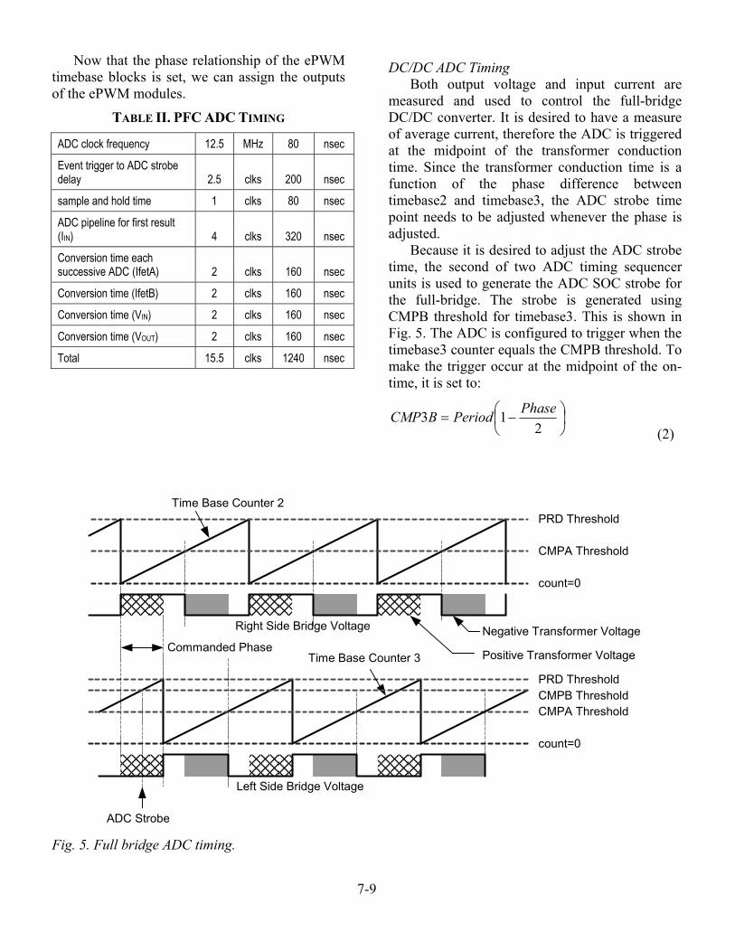
DC/DC ADC Timing Both output voltage and input current are
measured and used to control the full-bridge DC/DC converter. It is desired to have a measure of average current, therefore the ADC is triggered at the midpoint of the transformer conduction time. Since the transformer conduction time is a function of the phase difference between timebase2 and timebase3, the ADC strobe time point needs to be adjusted whenever the phase is adjusted.
Because it is desired to adjust the ADC strobe time, the second of two ADC timing sequencer units is used to generate the ADC SOC strobe for the full-bridge. The strobe is generated using CMPB threshold for timebase3. This is shown in Fig. 5. The ADC is configured to trigger when the timebase3 counter equals the CMPB threshold. To make the trigger occur at the midpoint of the on-time, it is set to:
⎟⎠⎞
⎜⎝⎛ −=
213 PhasePeriodBCMP
(2)
Right Side Bridge Voltage
Commanded PhaseTime Base Counter 3
Time Base Counter 2PRD Threshold
CMPA Threshold
CMPA Threshold
count=0
PRD Threshold
count=0
Positive Transformer Voltage
Left Side Bridge Voltage
ADC Strobe
Negative Transformer Voltage
CMPB Threshold
Fig. 5. Full bridge ADC timing.

7-10
IV. PHASE SHIFTED FULL BRIDGE POWER STAGE
This stage consists of the power MOSFETs Q21/Q22/Q23/Q24, main transformer T21, resonant inductor Llk, current sense transformer T22, output rectifiers D21/D22/D23/D24, output filter inductor L21 and output filter capacitor C21. This stage converts the dc bus voltage to a regulated 48V output. As indicated in Fig. 6, one signal measurement is needed to implement the control algorithm. This is the output voltage Vo, measured with an opto-coupler based isolated voltage sensing circuit. The dc bus source current Isw is measured for implementing current limiting.
The converter is controlled by the single voltage feedback loop. The system parameters used in this design are: • Output power POUT=1000 W • DC bus voltage VBUS =385 V • Switching frequency fSW=200 kHz • Voltage loop sampling frequency fS = 200 kHz • L21=8 μH • Llk=15 μH • C21=3 × 330 μF
The IR2110 gate driver IC was chosen because it features 600-V isolation on the high-side driver, which allows the high-side MOSFET to be driven directly from the driver.
The instantaneous signals VOUT and ISW are sensed and conditioned by the voltage and current sense circuits. The sensed signals are then fed back to the DSP via two ADC channels, ADCINB1 and ADCINB0, respectively. The sampling frequency for these signals is 200 kHz. The digitized sensed output voltage VOUT is then compared to the desired reference voltage VREF. The difference signal (VREF - VOUT) is then applied to the voltage loop controller G1. The digitized output of the controller G1, indicated as Vu, is used to generate the appropriate phase shift for the PWM signals applied to the diagonal switch pairs. The phase shift modulator block Pm is used to translate this control output into the phase shift information needed by the on-chip PWM hardware.
A. Output Voltage Sensing Circuit One feature of a digital power supply is the
ability to program a setpoint for the output voltage. For an isolated supply, this also poses a challenge. Typically, opto-coupler devices are used to bridge from secondary ground-referenced circuits to primary ground-referenced circuits. In a typical analog supply, the setpoint reference is compared with the output voltage feedback signal on the secondary side, and an amplified error voltage is transmitted through the opto-coupler. In this case, variation in opto-coupler gain will be compensated by the overall loop gain.
However, for a power supply with a digital feedback loop, we can calculate the error signal inside the processor so that setpoint can be programmed. Therefore, for an implementation like the telecom rectifier described here, in which the processor is on the primary side, a coupling circuit that has very little gain variation is required. The circuit shown in Fig. 7 is such a circuit. This circuit uses a HCNR200 opto-coupler that contains an LED and two photo detectors. The two photo detectors are split between the secondary and primary sides of the circuit.
This circuit delivers low gain variation by placing the LED-photo diode transfer function gain within the feedback loop of an operational amplifier. The analysis of the circuit proceeds as follows:
( )2
1
1R
vvvi
Avv
iGiiRvv
bberL
ab
Loptoo
omeasa
−−=
−=
=−=
(3)
Where Gopto is the LED-photo diode transfer current gain, A is the open loop gain of the op-amp and va, vb and vr are defined in Fig. 7.

7-11
D21 D23
T21
L21
C21
D22 D24
RL
ePWM2-A
ePWM2-B
ADCinB-1
PmG1++
_
VUVERR
VOUT
ADCinB-0
ePWM3-A
ePWM3-B
ISW
VREF
Digital Controller
IR2110
IR2110
T22
VO
+
VBUS
ISW Q23
Q24
Q21
Q22
LLK
Fig. 6. Simplified DC/DC converter stage implementation.
RF 56.2 kΩ
10 pF
R2301 Ω
0.1 μF
18.2 kΩiL
10 pF
R11 MΩ
11 V
VMEAS
iOiO'
VFBopto-PD2
iO
opto-PD1
Va Vb
OPA244
opto-LED
+
Fig. 7. Isolated, linear voltage feedback circuit.

7-12
Then
( )
( )omeasberopto
aberopto
o
iARAvvvR
G
AvvvR
Gi
12
2
−+−=
+−=
(5)
Solving for io
( ) ( )measopto
optober
opto
optoo v
RAGRAG
vvRAGR
Gi
1212 ++−
+=
For A>>1, this simplifies to
1Rvi meas
o = (6)
Assuming that the two photo-diodes are closely matched, the current gain from the LED to each diode should be matched as well. Therefore io' = io. For the output operational-amplifier.
f
fbo R
vi =' (7)
Then substituting io and solving for vfb yields the formula for the voltage gain of the linear opto-coupler circuit:
measf
fb vRR
v1
= (8)
For the telecom rectifier, R1=1.0 M and Rf=56.2 kΩ (both are 0.5% tolerance, yielding a gain tolerance of 0.7%). Therefore the transfer gain is 0.0562V/V. At vmeas=48 V, this generates 2.70 V at the 0 V to 3 V ADC input.
B. Calculation of Compensation Coefficients The voltage controller G1 is defined as a
second-order lead-lag compensator. It is implemented as a two-pole two-zero difference equation with coefficients:
22
11
22
110
1)(1 −−
−−
−−++
==zazazbzbb
EvUvzG (9)
To calculate the compensator coefficients, the desired continuous-time poles and zeros are defined along with a desired gain, and then converted to the discrete time domain using the bi-linear transformation.
TABLE III. COEFFICIENTS
gain 50 dB @ 1 kHz poles 0.01 Hz (near zero) 50 kHz (lag freq) zeros 800 Hz (lead freq) 1 MHz (> sample freq.)
A PC program has been developed that
accepts either the continuous-time lead-lag poles and zeros or the discrete-time difference equation coefficients as input, and downloads them to the hardware controller.
The implementation of the voltage loop controller is done as an assembly language macro. Expressed in terms of sample times, it has the following form:
)2(070.5)1(08026.0)(15.5)2(1202.0)1(1202.1)(
−−−++−−−=
nenenenununu
vvv
vvv
(10)
where
• uv(n) is the voltage controller output • ev(n) is the voltage error signal (VREF - VOUT).
Fig. 8 shows the transfer function of the
compensator. It shows a pole near zero forming the integrator, a zero at 800 Hz and another pole at 50 kHz forming the lead-lag compensation.
f - Frequency - Hz
-80
-60
-20
-100
Phas
e - d
egre
es
-40
-20
0
-40
40
60
20
10 100 1000 10 k 100 k
Gai
n - d
b
0
Fig. 8. DC/DC compensator frequency response.

7-13
Fig. 9. PC application for calculating compensator coefficients.
C. Calculation of Deadband Times For the phase shifted ZVS full-bridge
converter, the resonant transition time in each leg of the converter is different and, therefore, requires differing dead-times between the top and bottom switches. This is set by the on-chip dead-
band unit. The resonant transition time for the converter leg in which the two switches transition states (ON/OFF) after every power transfer cycle varies with load current. Therefore, variable dead-time is needed to extend ZVS operation to wide load range. This is achieved by constructing a look-up table with suitable dead-time values for different loads, and then adjusting accordingly during the runtime operation of the converter.
The load power can be estimated from the input power, based on the input dc bus voltage and current (ISW) information. The same DSP controls both the PFC and the DC/DC stages, so has access to the dc bus voltage data needed to estimate input power.
D. Gate Drive Safety Circuits
Trip Zones To provide safety over and above software
control, the UCD9501 features up to 6 trip zone inputs. The signals connected to these inputs are programmably routed to one or more of the PWM outputs. When a trip zone event occurs, the PWM output is disabled according to the logic described in Fig. 10.
Clear
Set
Sync
TripLogic
TZCTL[TZB]
TZCTL[TZB]
ePWMxB
ePWMxA
Trip
TZCTL[CBC]CTR=zero
TZFRC[CBC]TZ1TZ2TZ3TZ4TZ5TZ6
ePWMxA
ePWMxB
CBC Int
TZSEL[CBC1 to CBC6]
Latch cyc-by-cycmode (CBC)
Sync
TripTZCTL[OSHT]
TZFRC[OSHT]TZ1TZ2TZ3TZ4TZ5TZ6
TZSEL[OSTH1 to OSTH6]
Async Trip
OSHT int
Clear
SetLatch one-shotmode (OSHT)
Fig. 10. Trip zone enable logic.

7-14
DC/DC Full Bridge Trip Zone Safety Both the output voltage and input current are
monitored for the DC/DC converter. In each case, a PWM DAC is formed by driving current into a capacitor using the Enhanced Capture (eCAP) unit in the DSP as a PWM.
The behavior of this PWM DAC is described in Fig. 11 and in the following equations: At equilibrium, the current flowing into and out of the capacitor is equal. Therefore,
( )C
TDRv
CDT
Rvi
TC
IT
CI
sosoc
edischedisch
echech
−=⎟⎟
⎠
⎞⎜⎜⎝
⎛−
=
144
argarg
argarg
(11)
rearranging: DiRv co 4= The ripple is:
( )2
4
4
4
DDCTi
CDT
RIDRi
CDT
Rv
iv
scsc
soco
−=⎟⎟⎠
⎞⎜⎜⎝
⎛−=
⎟⎟⎠
⎞⎜⎜⎝
⎛−=Δ
(12)
(D-D2) is a maximum at D=0.5 where (D-D2) = 1/4.
Therefore,
CFiv
s
co 4=Δ
(13)
So for a desired maximum ripple of 1 mV, PWM frequency of 200 kHz, and 100 nF capacitor, the charge current should be 80 μA. Now, to set the maximum output voltage to ~3 V, set R4 to 37.4 kΩ. The charge current is defined as
( )beec vVRR
RR
ii −+
== 3.321
1
3
1 (14)
Therefore
cbe
c
iRvViRRR
33.3
312 −−= (15)
Setting R1 = R3 = 1.0k yields R2 = 31.6 kΩ. Given vbe temperature coefficient of -2.5 mV/°C,
( )[ ]
( )mVRR
RRRD
dtdv
TmVvVRR
RRRDv
o
beo
5.2
5.2
21
1
3
4
3.321
1
3
4
+=
+−+
= (16)
( )CmVDdtdvo °= /9.2
(17)
This yields ~3 LSBs/°C.
R11 kΩ
R31 kΩ
R231.6 kΩ
PWMOUT
Q1
Q2
Q2N3906Q2N3906
C1100 nF
R437.4 kΩ
VOUT
3V3
Fig. 11. Threshold setting PWM DAC.
V. SOFTWARE DESIGN
A. Overview The rectifier software is partitioned between C
and assembly code. The system consists of a background loop in C language, and a single ISR (interrupt service routine) in assembly language. This enables small tight code within the main high speed control ISR whilst allowing flexible high-level language for less critical tasks in the background loop (e.g., serial port handling, start-up/shut down management, fault management, and diagnostics). The ISR is subdivided into four time-slices by a simple time-slice manager state-machine. Although simple, this approach is efficient and very deterministic, ensuring all sampling and task execution occurs at known sub-multiples of the ISR frequency.

7-15
For this design, the ISR frequency chosen is 200 kHz. Fig. 13. shows the 200-kHz ISR with time-slices TS1, TS2, TS3 and TS4. Fig. 12 shows a flow diagram for the background loop.
MAIN
Initialization
28xx Device (i.e. system) levelPeripheral level
System levelFramework (ISR)
Interrupts
Startup/shutdownInstrumentation
Communications
Background Loop
Fig. 12. Background loop.
in outincr
SLEW_LIMIT 1DCDC_VloopRefSlewedDCDC_Vloop_ref
DCDC_VloopSlewRate
ref outfeedback
CNTL_2P2Z 1DCDC_PhaseCmd
DCDC_voltage_sample(AdcSeq2[0])
PSFB_DRV 2
ADC_SEQ2_DRVin out
(ADC ch8)(ADC ch9)
AdcSeq2[ ] buffer
phase TBPH3cmpB3
(TB3 phase reg.)(ADC Seq2 SOC)
Fig. 13. DC/DC macro blocks and pointer variable interconnections.
B. ISR Control Function The ISR is responsible for the main control
loops associated with the PFC and DC/DC stages. Because any computational delay introduces phase loss in the closed loop transfer function. Critical functions in the ISR are implemented as assembly language macros. These macros pass data from one block to the next by the use of a virtual net. In this way the functions can be thought of as wired together to pass data. In reality, each virtual net is simply a global variable, referenced within the macro with a pointer.
Fig. 13 shows a graphical model of the DC/DC control loop function. Each gray block represents an assembly macro and each named connecting line represents a pointer-based virtual net.
FW_Isr
Code executed every ISR cell
TS 2 TS 3TS 1 TS 4
50 kHz 50 kHz 50 kHz 50 kHz
Execute onTime Slice 1
PFC_CONTROLLERRead PFC phase A
current
Execute onTime Slice 2
UPDATE_PFC_ISHARERead PFC phase B
current
Execute onTime Slice 3
PFC_CONTROLLER
Execute onTime Slice 1
CALC_INV_VAVG2DATA_BUFFER
(debug only)
Return
200 kHz
Fig. 14. High-level ISR view.

7-16
VI. COMPARISON OF DIGITAL CONTROL TO ANALOG CONTROL
The UCC3895 is an industry-standard zero voltage switching full-bridge controller. It features the following: • Programmable output turn-on delay • Adaptive delay set • Bi-directional oscillator synchronization • Voltage-mode, peak current-mode, or average
current-mode control • Programmable soft-start/soft-stop and chip
disable via a single pin • 0% to 100% duty-cycle control • 7-MHz error amplifier • Operation to 1-MHz clock frequency • Typical 5-mA operating current at 500 kHz • Very low 150-μA current during UVLO
In the following section, these features are compared and contrasted with their digital implementation.
A. Programmable Output Turn-on Delay Analog Controller: The analog input DELAB
programs the dead time between switching of OUTA and OUTB, and DELCD programs the dead time between OUTC and OUTD. This delay is introduced between complementary outputs in the same leg of the external bridge. DELAB and DELCD are set by resistors. In operation DELAB sets the deadband time for the leading edge of each on-time when a differential voltage is applied to the transformer primary and DELCD sets the deadband time for the trailing edge of each on-time.
Digital controller: The deadband time is independently programmable for each of four events. 1. Leading edge of a positive differential voltage
across the transformer. 2. Leading edge of a negative differential voltage
across the transformer. 3. Trailing edge of a positive differential voltage
across the transformer. 4. Trailing edge of a negative differential voltage
across the transformer.
Each adjustment has a resolution of 10 ns ±0.01 ns.
B. Adaptive Delay Set
Analog Controller This function sets the ratio between the
maximum and minimum programmed output-delay dead time. When the ADS pin is directly connected to the CS pin, no delay modulation occurs. The maximum delay modulation occurs when ADS is grounded. In this case, delay time is four times longer when CS = 0 than when CS = 2.0 V (the peak-current threshold).
Digital Controller The sampled input current is used to define a
pointer into a look-up table. The output of the lookup table is four deadband times which are a function of converter current. The values in the table can be fixed during product development, computed during manufacturing test, or calculated based on self calibration.
C. Oscillator Synchronization Analog Controller: When used as an output,
SYNC can be used as a clock, which is the same as the device’s internal clock. When used as an input, SYNC overrides the chip’s internal oscillator and act as its clock signal. This feature allows synchronization of multiple power supplies.
Digital Controller SYNC-IN and SYNC-OUT pins are
implemented in the UCD9501 digital controller. These pins allow synchronization of the PWM units. SYNC-IN is connected to the ePMW1 time base. Additionally the timebase phase register, TBPHS1, can be used to adjust the phase of the controller outputs relative to the sync pulse, This allows multiple converter circuits to be phase offset with 10 ns resolution.

7-17
D. Voltage-Mode, Peak Current-Mode, or Average Current-Mode Control
Analog Controller The inverting input of the PWM Comparator
(RAMP) pin receives either the CT waveform in voltage and average current-mode controls, or the current signal (plus slope compensation) in peak current-mode control.
Digital Controller Either average current mode or voltage mode
operation is available. Peak current mode requires additional external hardware to implement. Fig. 15 shows one such example. Another example is to use a gate driver IC with an integral comparator and such as the UCD72xx drivers from Texas Instruments.
+
+
Trip Zone In
LP339
OPA350
SPI InterfaceDAC7811
PWMDriver Out ISW
RCS
Fig. 15. Peak current control circuit.
E. Programmable Soft-start/Soft-stop and Chip Disable
Analog Controller Disable Mode: A rapid shutdown of the chip is
accomplished by externally forcing the SS/DISB pin below 0.5 V, externally forcing REF below 4 V, or if VDD drops below the undervoltage lockout threshold.
If an overcurrent fault is sensed, a soft-stop is initiated. In this mode, SS/DISB sinks a constant current of (10 × IRT). The soft-stop continues until SS/DISB falls below 0.5 V. When any of these faults are detected, all outputs are forced to ground immediately.
Soft-start Mode. After a fault or disable condition has passed, VDD is above the start threshold, and/or SS/DISB falls below 0.5 V during a soft-stop, SS/DISB switches to a soft-start mode. The pin then sources current, equal to IRT. A user-selected resistor/capacitor combination on SS/DISB determines the soft start time constant.
Digital Controller Soft-start and soft-stop functions are
implemented by slew rate limiting any change to the setpoint reference. The slew rate itself is programmed, allowing different start or stop profiles for different events. To minimize transients, the firmware queries the current output voltage level before starting (or restarting after a fault) and sets the setpoint reference to the measured value before slewing to the desired final output voltage value.
F. Phase Shift Control Duty Cycle Range
Analog Controller 0% to 100% control is provided.
Digital Controller Limits on the amount of phase shift between
each half of the bridge can be adjusted by the firmware depending on the operating mode. For the present firmware version, the duty cycle limits are set to 5% and 95%.
G. Error Amplifier
Analog Controller BW = 7 MHz (typ), VOFFSET = 7 mV
Digital Controller BW set by Nyquist frequency (1/2 sample
rate). ADC offset = 4 LSB, corresponding to ~3 mV.
H. PWM Frequency
Analog Controller Operation to 1 MHz.
Digital Controller DC/DC loop control takes ~50 clock ticks, so
theoretical maximum PWM frequency is 2 MHz.

7-18
I. Current Requirements
Analog Controller Typical 5-mA operating current at 500 kHz.
150-μA during UVLO.
Digital Controller Maximum operating current is 260 mA at
1.8 V and 70 mA at 3.3 V (700 mW) Halt mode current is 120 μA at 1.8 V and 150 μA at 3.3 V (0.7 mW).
VII. TEST MEASUREMENTS Fig. 16. and Fig 17. are scope traces of the
primary voltage and current in the DC/DC bridge.
T - Time - 1 ms/div0
100
200
300
400
V WH
AT -
Wha
t Vol
tage
- V
Fig. 16. DC/DC bridge voltages.
T - Time - 1 ms/div
-200
0
200
400
-400V WH
AT -
Wha
t Vol
tage
- V
Fig 17. DC/DC transformer voltage and bridge input current.
The waveforms in Fig. 18. through Fig. 20. are signal traces captured by the digital controller.
IMEAS & ICMD
T - Time - 5 ms/div
VIN
- In
put V
olta
ge -
VI -
Cur
rent
- A
VBOOSTAC VIN
200
300
6
400
100
4
2
0
Fig. 18. PFC voltage and current waveforms.
Fig. 19. PFC start-up waveforms.

7-19
Fig. 20. DC/DC start-up waveforms.
As a diagnostic tool, random access memory (RAM) in the controller that is not used to generate the control effort, communication and other functions is allocated as a trace buffer. This buffer is simply a C-language array. In the digital telecom rectifier example the array is organized and is a four element wide by 2048 element deep array. Once every two to N ISR sample times, four variables are stored in the array and the array pointer is incremented.
Another valuable configuration of the trace buffer is to use it to capture a fault event. To do this set the trace buffer to free-run, (i.e. continually writing four variables to the buffer array and resetting the array pointer to the beginning each time it reaches the end of the array.) Then set the buffer control logic to stop on a fault event.
With this function enabled, infrequent events can be captured. This could be very valuable if the fault only occurs in the end-user system.
VIII. SUMMARY We have shown the details of the design of a
digitally controlled AC/DC power supply. The process of developing the design were broken down into seven steps, starting with defining the topology and ending with writing and debugging the digital controller firmware.
Digital control of a phase shifted full bridge is compared to analog. Digital control allows much more flexibility in defining start-up sequences and fault detection, but requires solid understanding of the effects of sampling on the feedback signals.
REFERENCES
[1] UCC3895 data sheet (SLUS157)
[2] UCD9501 datasheet (SPRS275)
[3] Fundamentals of Power Electronics, Erickson & Maksimović, 2001 Kluwer Academic Publishers
[4] Understanding Boost Power Stages in Switchmode Power Supplies, March 1999, Application Note, TI Literature Number (SLVA061)
[5] TMS320x280x DSP Analog-to-Digital Converter (ADC) Reference Guide, TI Literature Number (SPRU716)
[6] TMS320x280x Enhanced Pulse Width Modulator (ePWM) Module Reference Guide, TI Literature Number: (SPRU791)
[7] Average Current Mode Control of Switching Power Supplies, Unitrode Application Note U-140, TI Literature Number (SLUA079)
