tms320c674x/omap-l1x processor mmc/sd card … · 18 mmc memory clock control register...
TRANSCRIPT

TMS320C674x/OMAP-L1x ProcessorMultimedia Card (MMC)/Secure Digital (SD) Card Controller
User's Guide
Literature Number: SPRUFM2B
August 2010

2 SPRUFM2B–August 2010
Copyright © 2010, Texas Instruments Incorporated

Preface ....................................................................................................................................... 71 Introduction ........................................................................................................................ 9
1.1 Purpose of the Peripheral .............................................................................................. 9
1.2 Features .................................................................................................................. 9
1.3 Functional Block Diagram .............................................................................................. 9
1.4 Supported Use Case Statement ..................................................................................... 10
1.5 Industry Standard(s) Compliance Statement ....................................................................... 10
2 Architecture ...................................................................................................................... 112.1 Clock Control ........................................................................................................... 12
2.2 Signal Descriptions .................................................................................................... 13
2.3 Protocol Descriptions .................................................................................................. 14
2.4 Data Flow in the Input/Output FIFO ................................................................................. 16
2.5 Data Flow in the Data Registers (MMCDRR and MMCDXR) .................................................... 17
2.6 FIFO Operation During Card Read Operation ..................................................................... 18
2.7 FIFO Operation During Card Write Operation ..................................................................... 20
2.8 Reset Considerations .................................................................................................. 20
2.9 Initialization ............................................................................................................. 22
2.10 Interrupt Support ....................................................................................................... 25
2.11 DMA Event Support ................................................................................................... 26
2.12 Power Management ................................................................................................... 26
2.13 Emulation Considerations ............................................................................................. 26
3 Procedures for Common Operations .................................................................................... 273.1 Card Identification Operation ......................................................................................... 27
3.2 MMC/SD Mode Single-Block Write Operation Using CPU ....................................................... 30
3.3 MMC/SD Mode Single-Block Write Operation Using the EDMA ................................................ 32
3.4 MMC/SD Mode Single-Block Read Operation Using the CPU .................................................. 32
3.5 MMC/SD Mode Single-Block Read Operation Using EDMA ..................................................... 34
3.6 MMC/SD Mode Multiple-Block Write Operation Using CPU ..................................................... 34
3.7 MMC/SD Mode Multiple-Block Write Operation Using EDMA ................................................... 36
3.8 MMC/SD Mode Multiple-Block Read Operation Using CPU ..................................................... 36
3.9 MMC/SD Mode Multiple-Block Read Operation Using EDMA ................................................... 38
3.10 SDIO Card Function ................................................................................................... 38
4 Registers .......................................................................................................................... 394.1 MMC Control Register (MMCCTL) .................................................................................. 40
4.2 MMC Memory Clock Control Register (MMCCLK) ................................................................ 41
4.3 MMC Status Register 0 (MMCST0) ................................................................................. 42
4.4 MMC Status Register 1 (MMCST1) ................................................................................. 44
4.5 MMC Interrupt Mask Register (MMCIM) ............................................................................ 45
4.6 MMC Response Time-Out Register (MMCTOR) .................................................................. 47
4.7 MMC Data Read Time-Out Register (MMCTOD) .................................................................. 48
4.8 MMC Block Length Register (MMCBLEN) .......................................................................... 49
4.9 MMC Number of Blocks Register (MMCNBLK) .................................................................... 50
3SPRUFM2B–August 2010 Table of Contents
Copyright © 2010, Texas Instruments Incorporated

www.ti.com
4.10 MMC Number of Blocks Counter Register (MMCNBLC) ......................................................... 50
4.11 MMC Data Receive Register (MMCDRR) .......................................................................... 51
4.12 MMC Data Transmit Register (MMCDXR) .......................................................................... 51
4.13 MMC Command Register (MMCCMD) .............................................................................. 52
4.14 MMC Argument Register (MMCARGHL) ........................................................................... 54
4.15 MMC Response Registers (MMCRSP0-MMCRSP7) ............................................................. 55
4.16 MMC Data Response Register (MMCDRSP) ...................................................................... 57
4.17 MMC Command Index Register (MMCCIDX) ...................................................................... 57
4.18 SDIO Control Register (SDIOCTL) .................................................................................. 58
4.19 SDIO Status Register 0 (SDIOST0) ................................................................................. 59
4.20 SDIO Interrupt Enable Register (SDIOIEN) ........................................................................ 60
4.21 SDIO Interrupt Status Register (SDIOIST) ......................................................................... 60
4.22 MMC FIFO Control Register (MMCFIFOCTL) ..................................................................... 61
Appendix A Revision History ...................................................................................................... 62
4 Contents SPRUFM2B–August 2010
Copyright © 2010, Texas Instruments Incorporated

www.ti.com
List of Figures
1 MMC/SD Card Controller Block Diagram ................................................................................ 9
2 MMC/SD Controller Interface Diagram ................................................................................. 11
3 MMC Configuration and SD Configuration Diagram .................................................................. 12
4 MMC/SD Controller Clocking Diagram ................................................................................. 13
5 MMC/SD Mode Write Sequence Timing Diagram .................................................................... 14
6 MMC/SD Mode Read Sequence Timing Diagram .................................................................... 15
7 FIFO Operation Diagram ................................................................................................. 16
8 Little-Endian Access to MMCDXR/MMCDRR from the CPU or the EDMA........................................ 17
9 FIFO Operation During Card Read Diagram .......................................................................... 19
10 FIFO Operation During Card Write Diagram........................................................................... 21
11 MMC Card Identification Procedure..................................................................................... 28
12 SD Card Identification Procedure ....................................................................................... 29
13 MMC/SD Mode Single-Block Write Operation ......................................................................... 31
14 MMC/SD Mode Single-Block Read Operation......................................................................... 33
15 MMC/SD Multiple-Block Write Operation............................................................................... 35
16 MMC/SD Mode Multiple-Block Read Operation ....................................................................... 37
17 MMC Control Register (MMCCTL) ...................................................................................... 40
18 MMC Memory Clock Control Register (MMCCLK).................................................................... 41
19 MMC Status Register 0 (MMCST0) ..................................................................................... 42
20 MMC Status Register 1 (MMCST1) ..................................................................................... 44
21 MMC Interrupt Mask Register (MMCIM)................................................................................ 45
22 MMC Response Time-Out Register (MMCTOR) ...................................................................... 47
23 MMC Data Read Time-Out Register (MMCTOD) ..................................................................... 48
24 MMC Block Length Register (MMCBLEN) ............................................................................. 49
25 MMC Number of Blocks Register (MMCNBLK) ....................................................................... 50
26 MMC Number of Blocks Counter Register (MMCNBLC)............................................................. 50
27 MMC Data Receive Register (MMCDRR).............................................................................. 51
28 MMC Data Transmit Register (MMCDXR) ............................................................................. 51
29 MMC Command Register (MMCCMD) ................................................................................. 52
30 Command Format ......................................................................................................... 53
31 MMC Argument Register (MMCARGHL)............................................................................... 54
32 MMC Response Register 0 and 1 (MMCRSP01) ..................................................................... 55
33 MMC Response Register 2 and 3 (MMCRSP23) ..................................................................... 55
34 MMC Response Register 4 and 5 (MMCRSP45) ..................................................................... 55
35 MMC Response Register 6 and 7 (MMCRSP67) ..................................................................... 55
36 MMC Data Response Register (MMCDRSP).......................................................................... 57
37 MMC Command Index Register (MMCCIDX).......................................................................... 57
38 SDIO Control Register (SDIOCTL)...................................................................................... 58
39 SDIO Status Register 0 (SDIOST0)..................................................................................... 59
40 SDIO Interrupt Enable Register (SDIOIEN)............................................................................ 60
41 SDIO Interrupt Status Register (SDIOIST)............................................................................. 60
42 MMC FIFO Control Register (MMCFIFOCTL) ......................................................................... 61
5SPRUFM2B–August 2010 List of Figures
Copyright © 2010, Texas Instruments Incorporated

www.ti.com
List of Tables
1 MMC/SD Controller Pins Used in Each Mode ......................................................................... 13
2 MMC/SD Mode Write Sequence ........................................................................................ 14
3 MMC/SD Mode Read Sequence ........................................................................................ 15
4 Description of MMC/SD Interrupt Requests............................................................................ 25
5 Multimedia Card/Secure Digital (MMC/SD) Card Controller Registers............................................. 39
6 MMC Control Register (MMCCTL) Field Descriptions................................................................ 40
7 MMC Memory Clock Control Register (MMCCLK) Field Descriptions ............................................. 41
8 MMC Status Register 0 (MMCST0) Field Descriptions............................................................... 42
9 MMC Status Register 1 (MMCST1) Field Descriptions............................................................... 44
10 MMC Interrupt Mask Register (MMCIM) Field Descriptions ......................................................... 45
11 MMC Response Time-Out Register (MMCTOR) Field Descriptions................................................ 47
12 MMC Data Read Time-Out Register (MMCTOD) Field Descriptions............................................... 48
13 MMC Block Length Register (MMCBLEN) Field Descriptions....................................................... 49
14 MMC Number of Blocks Register (MMCNBLK) Field Descriptions ................................................. 50
15 MMC Number of Blocks Counter Register (MMCNBLC) Field Descriptions ...................................... 50
16 MMC Data Receive Register (MMCDRR) Field Descriptions ....................................................... 51
17 MMC Data Transmit Register (MMCDXR) Field Descriptions ....................................................... 51
18 MMC Command Register (MMCCMD) Field Descriptions ........................................................... 52
19 Command Format ......................................................................................................... 53
20 MMC Argument Register (MMCARGHL) Field Descriptions......................................................... 54
21 R1, R3, R4, R5, or R6 Response (48 Bits) ............................................................................ 56
22 R2 Response (136 Bits) .................................................................................................. 56
23 MMC Data Response Register (MMCDRSP) Field Descriptions ................................................... 57
24 MMC Command Index Register (MMCCIDX) Field Descriptions ................................................... 57
25 SDIO Control Register (SDIOCTL) Field Descriptions ............................................................... 58
26 SDIO Status Register 0 (SDIOST0) Field Descriptions .............................................................. 59
27 SDIO Interrupt Enable Register (SDIOIEN) Field Descriptions ..................................................... 60
28 SDIO Interrupt Status Register (SDIOIST) Field Descriptions ...................................................... 60
29 MMC FIFO Control Register (MMCFIFOCTL) Field Descriptions................................................... 61
30 Document Revision History .............................................................................................. 62
6 List of Tables SPRUFM2B–August 2010
Copyright © 2010, Texas Instruments Incorporated

PrefaceSPRUFM2B–August 2010
Read This First
About This Manual
This manual describes the multimedia card (MMC)/secure digital (SD) card controller. The MMC/SD cardis used in a number of applications to provide removable data storage. The MMC/SD controller providesan interface to external MMC and SD cards. The MMC/SD protocol performs the communication betweenthe MMC/SD controller and MMC/SD card(s).
Notational Conventions
This document uses the following conventions.
• Hexadecimal numbers are shown with the suffix h. For example, the following number is 40hexadecimal (decimal 64): 40h.
• Registers in this document are shown in figures and described in tables.
– Each register figure shows a rectangle divided into fields that represent the fields of the register.Each field is labeled with its bit name, its beginning and ending bit numbers above, and itsread/write properties below. A legend explains the notation used for the properties.
– Reserved bits in a register figure designate a bit that is used for future device expansion.
Related Documentation From Texas Instruments
The following documents describe the TMS320C674x Digital Signal Processors (DSPs) and OMAP-L1xApplications Processors. Copies of these documents are available on the Internet at www.ti.com. Tip:Enter the literature number in the search box provided at www.ti.com.
The current documentation that describes the DSP, related peripherals, and other technical collateral, isavailable in the C6000 DSP product folder at: www.ti.com/c6000.
SPRUGM5 — TMS320C6742 DSP System Reference Guide. Describes the C6742 DSP subsystem,system memory, device clocking, phase-locked loop controller (PLLC), power and sleep controller(PSC), power management, and system configuration module.
SPRUGJ0 — TMS320C6743 DSP System Reference Guide. Describes the System-on-Chip (SoC)including the C6743 DSP subsystem, system memory, device clocking, phase-locked loopcontroller (PLLC), power and sleep controller (PSC), power management, and system configurationmodule.
SPRUFK4 — TMS320C6745/C6747 DSP System Reference Guide. Describes the System-on-Chip(SoC) including the C6745/C6747 DSP subsystem, system memory, device clocking, phase-lockedloop controller (PLLC), power and sleep controller (PSC), power management, and systemconfiguration module.
SPRUGM6 — TMS320C6746 DSP System Reference Guide. Describes the C6746 DSP subsystem,system memory, device clocking, phase-locked loop controller (PLLC), power and sleep controller(PSC), power management, and system configuration module.
SPRUGJ7 — TMS320C6748 DSP System Reference Guide. Describes the C6748 DSP subsystem,system memory, device clocking, phase-locked loop controller (PLLC), power and sleep controller(PSC), power management, and system configuration module.
SPRUG84 — OMAP-L137 Applications Processor System Reference Guide. Describes theSystem-on-Chip (SoC) including the ARM subsystem, DSP subsystem, system memory, deviceclocking, phase-locked loop controller (PLLC), power and sleep controller (PSC), powermanagement, ARM interrupt controller (AINTC), and system configuration module.
7SPRUFM2B–August 2010 Preface
Copyright © 2010, Texas Instruments Incorporated

Related Documentation From Texas Instruments www.ti.com
SPRUGM7 — OMAP-L138 Applications Processor System Reference Guide. Describes theSystem-on-Chip (SoC) including the ARM subsystem, DSP subsystem, system memory, deviceclocking, phase-locked loop controller (PLLC), power and sleep controller (PSC), powermanagement, ARM interrupt controller (AINTC), and system configuration module.
SPRUFK9 — TMS320C674x/OMAP-L1x Processor Peripherals Overview Reference Guide. Providesan overview and briefly describes the peripherals available on the TMS320C674x Digital SignalProcessors (DSPs) and OMAP-L1x Applications Processors.
SPRUFK5 — TMS320C674x DSP Megamodule Reference Guide. Describes the TMS320C674x digitalsignal processor (DSP) megamodule. Included is a discussion on the internal direct memory access(IDMA) controller, the interrupt controller, the power-down controller, memory protection, bandwidthmanagement, and the memory and cache.
SPRUFE8 — TMS320C674x DSP CPU and Instruction Set Reference Guide. Describes the CPUarchitecture, pipeline, instruction set, and interrupts for the TMS320C674x digital signal processors(DSPs). The C674x DSP is an enhancement of the C64x+ and C67x+ DSPs with addedfunctionality and an expanded instruction set.
SPRUG82 — TMS320C674x DSP Cache User's Guide. Explains the fundamentals of memory cachesand describes how the two-level cache-based internal memory architecture in the TMS320C674xdigital signal processor (DSP) can be efficiently used in DSP applications. Shows how to maintaincoherence with external memory, how to use DMA to reduce memory latencies, and how tooptimize your code to improve cache efficiency. The internal memory architecture in the C674xDSP is organized in a two-level hierarchy consisting of a dedicated program cache (L1P) and adedicated data cache (L1D) on the first level. Accesses by the CPU to the these first level cachescan complete without CPU pipeline stalls. If the data requested by the CPU is not contained incache, it is fetched from the next lower memory level, L2 or external memory.
SD is a trademark of SanDisk Corporation.
8 Read This First SPRUFM2B–August 2010
Copyright © 2010, Texas Instruments Incorporated

Statusand
registersFIFO
CLKdivider
MMC/SDinterface
MMC/SDcardinterface
CPU
DMA requests
Interrupts
User's GuideSPRUFM2B–August 2010
Multimedia Card (MMC)/Secure Digital (SD) CardController
1 Introduction
This document describes the multimedia card (MMC)/secure digital (SD) card controller.
1.1 Purpose of the Peripheral
A number of applications use the multimedia card (MMC)/secure digital (SD) card to provide removabledata storage. The MMC/SD card controller provides an interface to external MMC and SD cards. Thecommunication between the MMC/SD card controller and MMC/SD card(s) is performed according to theMMC/SD protocol.
1.2 Features
The MMC/SD card controller has the following features:• Supports interface to multimedia cards (MMC)• Supports interface to secure digital (SD) memory cards• Ability to use the MMC/SD protocol and Secure Digital Input Output (SDIO) protocol• Programmable frequency of the clock that controls the timing of transfers between the MMC/SD
controller and memory card• 512-bit read/write FIFO to lower system overhead• Signaling to support enhanced direct memory access (EDMA) transfers (slave)• 20 MHz maximum clock to MMC• 25 MHz maximum clock to SD
1.3 Functional Block Diagram
The MMC/SD card controller transfers data between the CPU and the EDMA controller on one side andthe MMC/SD card on the other side, as shown in Figure 1. This means you have a choice of performingdata transfers using the CPU or EDMA as a mechanism to move data between the device memory andthe FIFO. The CPU and the EDMA controller can read from or write to the data in the card by accessingthe registers in the MMC/SD controller.
Figure 1. MMC/SD Card Controller Block Diagram
9SPRUFM2B–August 2010 Multimedia Card (MMC)/Secure Digital (SD) Card Controller
Copyright © 2010, Texas Instruments Incorporated

Introduction www.ti.com
1.4 Supported Use Case Statement
The MMC/SD card controller supports the following user cases:• MMC/SD card identification• MMC/SD single-block read using CPU• MMC/SD single-block read using EDMA• MMC/SD single-block write using CPU• MMC/SD single-block write using EDMA• MMC/SD multiple-block read using CPU• MMC/SD multiple-block read using EDMA• MMC/SD multiple-block write using CPU• MMC/SD multiple-block write using EDMA
1.5 Industry Standard(s) Compliance Statement
The MMC/SD card controller supports the following industry standards (with the exception noted below):
• MMC (Multimedia Card) Specification v4.0• SD (Secure Digital) Physical Layer Specification v1.1• SDIO (Secure Digital Input Output) Specification v2.0
The information in this document assumes that you are familiar with these standards.
The MMC/SD controller does not support the SPI mode of operation.
10 Multimedia Card (MMC)/Secure Digital (SD) Card Controller SPRUFM2B–August 2010
Copyright © 2010, Texas Instruments Incorporated

Native packets
Nativesignals
CMD
DAT0, DAT0-3,or DAT0-7
CLK
EDMA
CPU
Memory
MMCs or SD cards
MMC/SDcontroller
www.ti.com Architecture
2 Architecture
The MMC/SD controller uses the MMC/SD protocol to communicate with the MMC/SD cards. You canconfigure the MMC/SD controller to work as an MMC or SD controller, based on the type of card thecontroller is communicating with. Figure 2 summarizes the MMC/SD mode interface. Figure 3 illustrateshow the controller interfaces to the cards in MMC/SD mode.
In the MMC/SD mode, the MMC controller supports one or more MMC/SD cards. Regardless of thenumber of cards connected, the MMC/SD controller selects one by using identification broadcast on thedata line. The following MMC/SD controller pins are used:• MMCSD_CMD: This pin is used for two-way communication between the connected card and the
MMC/SD controller. The MMC/SD controller transmits commands to the card and the memory carddrives responses to the commands on this pin.
• MMCSD_DAT0, MMCSD_DAT0-3, or MMCSD_DAT0-7: MMC cards only use one data line (DAT0),four data lines (DAT0-3), or eight data lines (DAT0-7), and SD cards use one data line (DAT0) or fourdata lines (DAT0-3). The number of MMCSD_DAT pins (the data bus width) is set by the WIDTH bit inthe MMC control register (MMCCTL), see Section 4.1).
• MMCSD_CLK: This pin provides the clock to the memory card from the MMC/SD controller.
Figure 2. MMC/SD Controller Interface Diagram
11SPRUFM2B–August 2010 Multimedia Card (MMC)/Secure Digital (SD) Card Controller
Copyright © 2010, Texas Instruments Incorporated

CLK
CMD
DAT0
DAT1
DAT2
DAT3
DAT4
DAT5
DAT6
DAT7
CLK
CMD
DAT0
DAT1
DAT2
DAT3
DAT4
DAT5
DAT6
DAT7
MMC/SD controller MMC card (8-bit mode)
MMC configuration
CLK
CMD
DAT0
CLK
CMD
DAT0
MMC/SD controller MMC and SD (1-bit mode)
MMC/SD configuration
MMC/SD configuration
CLK
CMD
DAT0
DAT1
DAT2
DAT3
DAT4
DAT5
DAT6
DAT7
CLK
CMD
DAT0
DAT1
DAT2
DAT3
MMC/SD controller MMC and SD (4-bit mode)
DAT1
DAT2
DAT3
DAT4
DAT5
DAT6
DAT7
Architecture www.ti.com
Figure 3. MMC Configuration and SD Configuration Diagram
2.1 Clock Control
There are two clocks, the function clock and the memory clock, in the MMC/SD controller (Figure 4).
The function clock determines the operational frequency of the MMC/SD controller and is the input clockto the MMC/SD card(s).
12 Multimedia Card (MMC)/Secure Digital (SD) Card Controller SPRUFM2B–August 2010
Copyright © 2010, Texas Instruments Incorporated

MMCCLK(CLKRT)
Function clock forMMC/SD controller
MMC/SD controller
MMC/SDinput clock card
MMC/SD
Memory clockon CLK pin
www.ti.com Architecture
The memory clock appears on the MMCSD_CLK pin of the MMC/SD controller interface. The memoryclock controls the timing of communication between the MMC/SD controller and the connected memorycard. The memory clock is generated by dividing the function clock in the MMC/SD controller. Thedivide-down value is set by CLKRT bits in the MMC memory clock control register (MMCCLK) and isdetermined by the following equation:
memory clock frequency = function clock frequency/(2 × (CLKRT + 1))
Figure 4. MMC/SD Controller Clocking Diagram
(1) Maximum memory clock frequency in MMC card can be 20 MHz.
(2) Maximum memory clock frequency in SD card can be 50 MHz.
2.2 Signal Descriptions
Table 1 shows the MMC/SD controller pins that each mode uses. The MMC/SD protocol uses the clock,command (two-way communication between the MMC controller and memory card), and data(MMCSD_DAT0, MMCSD_DAT0-3, or MMCSD_DAT0-7 for MMC card; MMCSD_DAT0 orMMCSD_DAT0-3 for SD card) pins.
Table 1. MMC/SD Controller Pins Used in Each Mode
Function
MMC and SD (1-bit mode) MMC and SD (4-bit mode) MMC (8-bit mode)Pin Type (1) Communications Communications Communication
MMCSD_CLK O Clock line Clock line Clock line
MMCSD_CMD I/O Command line Command line Command line
MMCSD_DAT0 I/O Data line 0 Data line 0 Data line 0
MMCSD_DAT1 I/O (Not used) Data line 1 Data line 1
MMCSD_DAT2 I/O (Not used) Data line 2 Data line 2
MMCSD_DAT3 I/O (Not used) Data line 3 Data line 3
MMCSD_DAT4 I/O (Not used) Data line 4
MMCSD_DAT5 I/O (Not used) Data line 5
MMCSD_DAT6 I/O (Not used) Data line 6
MMCSD_DAT7 I/O (Not used) Data line 7(1) I = input to the MMC controller; O = output from the MMC controller.
13SPRUFM2B–August 2010 Multimedia Card (MMC)/Secure Digital (SD) Card Controller
Copyright © 2010, Texas Instruments Incorporated

2 CRC bytesBusylow
Startbit
Endbit
Startbit
Endbit
CMD
Data
CLK
Architecture www.ti.com
2.3 Protocol Descriptions
The MMC/SD controller follows the MMC/SD protocol for completing any kind of transaction with themultimedia card and secure digital cards. For more detailed information, refer to the supported MMC andSD specifications in Section 1.5.
2.3.1 MMC/SD Mode Write Sequence
Figure 5 and Table 2 show the signal activity when the MMC/SD controller is in the MMC/SD mode and iswriting data to a memory card. The same block length must be defined in the MMC/SD controller and inthe memory card before initiating a data write. In a successful write protocol sequence, the following stepsoccur:• The MMC/SD controller requests the CSD content.• The card receives the command and sends the content of the CSD register as its response.• If the desired block length, WRITE_BL_LEN value, is different from the default value determined from
the response, the MMC/SD controller sends the block length command.• The card receives the command and sends responses to the command.• The MMC/SD controller requests the card to change states from standby to transfer.• The card receives the command and sends responses to the command.• The MMC/SD controller sends a write command to the card.• The card receives the command and sends responses to the command.• The MMC/SD controller sends a block of data to the card.• The card sends the CRC status to the MMC/SD controller.• The card sends a low BUSY bit until all of the data has been programmed into the flash memory inside
the card.
Figure 5. MMC/SD Mode Write Sequence Timing Diagram
Table 2. MMC/SD Mode Write Sequence
Portion of theSequence Description
WR CMD Write command: A 6-byte WRITE_BLOCK command token is sent from the CPU to the card.
CMD RSP Command response: The card sends a 6-byte response of type R1 to acknowledge the WRITE_BLOCK to theCPU.
DAT BLK Data block: The CPU writes a block of data to the card. The data content is preceded by one start bit and isfollowed by two CRC bytes and one end bit.
CRC STAT CRC status: The card sends a one byte CRC status information, which indicates to the CPU whether the data hasbeen accepted by the card or rejected due to a CRC error. The CRC status information is preceded by one startbit and is followed by one end bit.
BSY BUSY bit: The CRC status information is followed by a continuous stream of low busy bits until all of the data hasbeen programmed into the flash memory on the card.
14 Multimedia Card (MMC)/Secure Digital (SD) Card Controller SPRUFM2B–August 2010
Copyright © 2010, Texas Instruments Incorporated

Startbit
Endbit
CMD
Data
CLK
1 transfersource bit
2 CRCbytes
www.ti.com Architecture
2.3.2 MMC/SD Mode Read Sequence
Figure 6 and Table 3 show the signal activity when the MMC controller is in the MMC/SD mode and isreading data from a memory card. The same block length must be defined in the MMC controller and inthe memory card before initiating a data read. In a successful read protocol sequence, the following stepsoccur:• The MMC/SD controller requests for the CSD content.• The card receives the command and sends the content of the CSD register as its response.• If the desired block length, READ_BL_LEN value, is different from the default value determined from
the response, the MMC/SD controller sends the block length command.• The card receives the command and sends responses to the command.• The MMC/SD controller requests the card to change state from stand-by to transfer.• The card receives the command and sends responses to the command.• The MMC/SD controller sends a read command to the card.• The card drives responses to the command.• The card sends a block of data to the CPU.
Figure 6. MMC/SD Mode Read Sequence Timing Diagram
Table 3. MMC/SD Mode Read Sequence
Portion of theSequence Description
RD CMD Read command: A 6-byte READ_SINGLE_BLOCK command token is sent from the CPU to the card.
CMD RSP Command response: The card sends a response of type R1 to acknowledge the READ_SINGLE_BLOCKcommand to the CPU.
DAT BLK Data block: The card sends a block of data to the CPU. The data content is preceded by a start bit and is followedby two CRC byte and an end bit.
15SPRUFM2B–August 2010 Multimedia Card (MMC)/Secure Digital (SD) Card Controller
Copyright © 2010, Texas Instruments Incorporated

8-bit x 64(512-bit)
FIFO
EDMA event256 or 512 bits
EDMA event256 or 512 bits
EDMA eventthe end of atransfer
Pointer incrementor decrease
FIFO
WriteEDMArequest
is created
Pointer incrementor decrease
FIFO
Read
CPU/EDMA reads/writes
16-bit DXRshifter
16-bit DRRshifter
16-bit DXR 16-bit DRR
DXR DRR
Transmission of data
Step 1:Step 2:Step 3:Step 4:
Set FIFO resetSet FIFO directionEDMA driven transactionCPU driven transaction:Fill the FIFO by writing toMMCDXR (only first time)or every 256 or 512-bitstransmitted and DXRDYINTinterrupt is generated
Step 5:Step 6:
EDMA send xmit dataIf DXR ready is active,FIFO -> 16-bit DXR
Reception of data
Step 1:Step 2:Step 3:
Set FIFO resetSet FIFO directionIf DRR ready is active,16-bit DRR -> FIFO
Step 4:Step 5:
EDMA driven transactionDRRDYINT interrupt occurwhen FIFO every 256 or512-bits of data receivedby FIFO
Step 6: EDMA read reception data
Architecture www.ti.com
2.4 Data Flow in the Input/Output FIFO
The MMC/SD controller contains a single 512-bit FIFO, organized as 8-bit × 64 entries, that is used forboth reading data from the memory card and writing data to the memory card (see Figure 7). Theconversion from the 32-bit bus to the byte format of the FIFO follows the little-endian convention (detailsare provided in later sections). The read and write FIFOs act as an interim location to store datatransferred from/to the card momentarily via the CPU or EDMA. The FIFO includes logic to generateEDMA events and interrupts based on the amount of data in the FIFO and a programmable number ofbytes received/transmitted. Flags are set when the FIFO is full or empty.
A high-level operational description is as follows:• Data is written to the FIFO through the MMC data transmit register (MMCDXR). Data is read from the
FIFO through the MMC data receive register (MMCDRR). This is true for both the CPU and EDMAdriven transactions; however, for the EDMA transaction, the EDMA access to the FIFO is transparent.
• The ACCWD bits in the MMC FIFO control register (MMCFIFOCTL) determines the behavior of theFIFO full (FIFOFUL) and FIFO empty (FIFOEMP) status flags in the MMC status register 1 (MMCST1):
– If ACCWD = 00b:
• FIFO full is active when the write pointer + 4 > read pointer• FIFO empty is active when the write pointer - 4 < read pointer
– If ACCWD = 01b:
• FIFO full is active when the write pointer + 3 > read pointer• FIFO empty is active when the write pointer - 3 < read pointer
– If ACCWD = 10b:
• FIFO full is active when the write pointer + 2 > read pointer• FIFO empty is active when the write pointer - 2 < read pointer
– If ACCWD = 11b:
• FIFO full is active when the write pointer + 1 > read pointer• FIFO empty is active when the write pointer - 1 < read pointer
Figure 7. FIFO Operation Diagram
16 Multimedia Card (MMC)/Secure Digital (SD) Card Controller SPRUFM2B–August 2010
Copyright © 2010, Texas Instruments Incorporated

1st
2nd
3rd
4th
3
4th 3rd 2nd 1st
Support byten = ”1111”
Support byten = ”0111”
3rd
2nd
1st
3
3rd 2nd 1st
Support byten = ”0011”
1st
2nd
3
2nd 1st
0
Support byten = ”0001”
1st
3
1st
0
0
0
FIFO MMCDRR or MMCDXR registers
www.ti.com Architecture
2.5 Data Flow in the Data Registers (MMCDRR and MMCDXR)
The CPU or EDMA controller can read 32 bits at a time from the FIFO by reading the MMC data receiveregister (MMCDRR) and write 32 bits at a time to the FIFO by writing to the MMC data transmit register(MMCDXR). However, since the memory card is an 8-bit device, it transmits or receives one byte at atime. Figure 8 shows how the data size is handled by the data registers in little-endian mode.
Figure 8. Little-Endian Access to MMCDXR/MMCDRR from the CPU or the EDMA
17SPRUFM2B–August 2010 Multimedia Card (MMC)/Secure Digital (SD) Card Controller
Copyright © 2010, Texas Instruments Incorporated

Architecture www.ti.com
2.6 FIFO Operation During Card Read Operation
2.6.1 EDMA Reads
The FIFO controller manages the activities of reading the data in from the card and issuing EDMA readevents. Each time an EDMA read event is issued, an EDMA read request interrupt generates.
Figure 9 provides details of the FIFO controllers operation. As data is received from the card, it is read intothe FIFO. When the number of bytes of data received is equal to the level set by the FIFOLEV bits inMMCFIFOCTL, an EDMA read event is issued and new EDMA events are disabled until the EDMA isdone with the transfer issued by the current event. Data is read from the FIFO by way of MMCDRR. TheFIFO controller continues to read in data from the card while checking for the EDMA event to occur or forthe FIFO to become full. Once the EDMA event finishes, new EDMA events are enabled. If the FIFO fillsup, the FIFO controller stops the MMC/SD controller from reading any more data until the FIFO is nolonger full.
An EDMA read event generates when the last data arrives, as determined by the MMC block lengthregister (MMCBLEN) and the MMC number of blocks register (MMCNBLK) settings. This EDMA eventflushes all of the data that was read from the card from the FIFO.
Each time an EDMA read event generates, an interrupt (DRRDYINT) generates and the DRRDY bit in theMMC status register 0 (MMCST0) is also set.
2.6.2 CPU Reads
The system CPU can also directly read the card data by reading the MMC data receive register(MMCDRR). The MMC/SD peripheral supports reads that are 1-, 2-, 3-, or 4-bytes wide as, shown inFigure 8.
As data is received from the card, it is read into the FIFO. When the number of bytes of data received isequal to the level set by the FIFOLEV bits in MMCFIFOCTL, a DRRDYINT interrupt is issued and theDRRDY bit in the MMC status register 0 (MMCST0) is set. Upon receiving the interrupt, the CPU quicklyreads out the bytes received (equal to the level set by the FIFOLEV bits). A DRRDYINT interrupt alsogenerates when the last data arrives as determined by the MMC block length register (MMCBLEN) andthe MMC numbers of blocks register (MMCNBLK) settings.
18 Multimedia Card (MMC)/Secure Digital (SD) Card Controller SPRUFM2B–August 2010
Copyright © 2010, Texas Instruments Incorporated

FIFO Check1/Start
FIFOfull?
Counter=FIFOLEV
?
Yes
No
Capture data,no DMA pending
Increment counter
No
Yes
Generate DMA
Reset counter
FIFO check 2
Yes
No
?full
FIFO
No
=FIFOLEV?
Counter
Increment counter
DMACapture data,
done?
DMANo
Yes
Yes
Yes
Generate DMA
Reset counter
Idle, DMA pending
DMANodone
?
www.ti.com Architecture
Figure 9. FIFO Operation During Card Read Diagram
19SPRUFM2B–August 2010 Multimedia Card (MMC)/Secure Digital (SD) Card Controller
Copyright © 2010, Texas Instruments Incorporated
Architecture www.ti.com
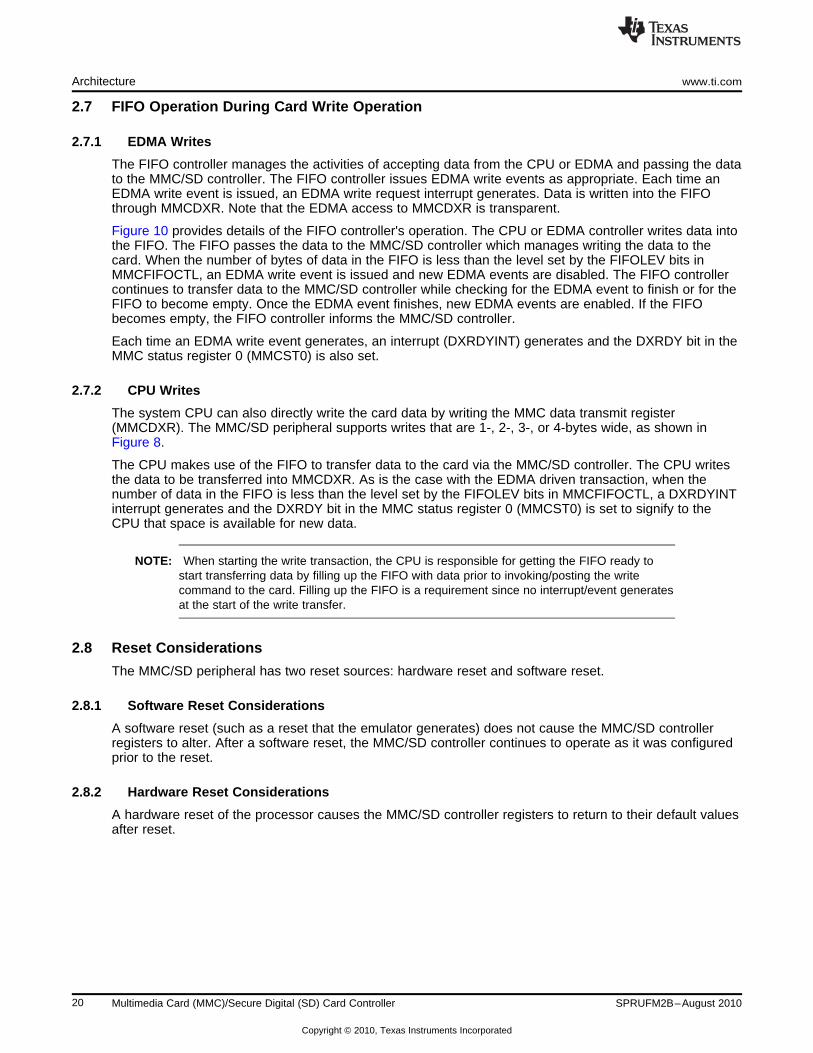
2.7 FIFO Operation During Card Write Operation
2.7.1 EDMA Writes
The FIFO controller manages the activities of accepting data from the CPU or EDMA and passing the datato the MMC/SD controller. The FIFO controller issues EDMA write events as appropriate. Each time anEDMA write event is issued, an EDMA write request interrupt generates. Data is written into the FIFOthrough MMCDXR. Note that the EDMA access to MMCDXR is transparent.
Figure 10 provides details of the FIFO controller's operation. The CPU or EDMA controller writes data intothe FIFO. The FIFO passes the data to the MMC/SD controller which manages writing the data to thecard. When the number of bytes of data in the FIFO is less than the level set by the FIFOLEV bits inMMCFIFOCTL, an EDMA write event is issued and new EDMA events are disabled. The FIFO controllercontinues to transfer data to the MMC/SD controller while checking for the EDMA event to finish or for theFIFO to become empty. Once the EDMA event finishes, new EDMA events are enabled. If the FIFObecomes empty, the FIFO controller informs the MMC/SD controller.
Each time an EDMA write event generates, an interrupt (DXRDYINT) generates and the DXRDY bit in theMMC status register 0 (MMCST0) is also set.
2.7.2 CPU Writes
The system CPU can also directly write the card data by writing the MMC data transmit register(MMCDXR). The MMC/SD peripheral supports writes that are 1-, 2-, 3-, or 4-bytes wide, as shown inFigure 8.
The CPU makes use of the FIFO to transfer data to the card via the MMC/SD controller. The CPU writesthe data to be transferred into MMCDXR. As is the case with the EDMA driven transaction, when thenumber of data in the FIFO is less than the level set by the FIFOLEV bits in MMCFIFOCTL, a DXRDYINTinterrupt generates and the DXRDY bit in the MMC status register 0 (MMCST0) is set to signify to theCPU that space is available for new data.
NOTE: When starting the write transaction, the CPU is responsible for getting the FIFO ready tostart transferring data by filling up the FIFO with data prior to invoking/posting the writecommand to the card. Filling up the FIFO is a requirement since no interrupt/event generatesat the start of the write transfer.
2.8 Reset Considerations
The MMC/SD peripheral has two reset sources: hardware reset and software reset.
2.8.1 Software Reset Considerations
A software reset (such as a reset that the emulator generates) does not cause the MMC/SD controllerregisters to alter. After a software reset, the MMC/SD controller continues to operate as it was configuredprior to the reset.
2.8.2 Hardware Reset Considerations
A hardware reset of the processor causes the MMC/SD controller registers to return to their default valuesafter reset.
20 Multimedia Card (MMC)/Secure Digital (SD) Card Controller SPRUFM2B–August 2010
Copyright © 2010, Texas Instruments Incorporated

FIFO Check 1 / Start
FIFOempty
?
Counter=FIFOLEV
?
Yes
No
Send data,no DMA pending
Increment counter
No
Yes
Generate DMA
Reset counter
FIFO check 2
Yes
No
?emptyFIFO
No
=FIFOLEV?
Counter
Increment counter
DMA pendingSend data,
done?
DMANo
Yes
Yes
Yes
Generate DMA
Reset counter
Idle, DMA pending
DMANodone
?
www.ti.com Architecture
Figure 10. FIFO Operation During Card Write Diagram
21SPRUFM2B–August 2010 Multimedia Card (MMC)/Secure Digital (SD) Card Controller
Copyright © 2010, Texas Instruments Incorporated

Architecture www.ti.com
2.9 Initialization
2.9.1 MMC/SD Controller Initialization
The general procedure for initializing the MMC/SD controller is given in the following steps. Details aboutthe registers or register bit fields to be configured in the MMC/SD mode are in the subsequentsubsections.
1. Place the MMC/SD controller in its reset state by setting the CMDRST bit and DATRST bit in the MMCcontrol register (MMCCTL). You can set other bits in MMCCTL after reset.
2. Write the required values to other registers to complete the MMC/SD controller configuration.3. Clear the CMDRST bit and the DATRST bit in MMCCTL to release the MMC/SD controller from its
reset state. It is recommended not to rewrite the values that are written to the other bits of MMCCTL in.
4. Enable the MMCSD_CLK pin so that the memory clock is sent to the memory card by setting theCLKEN bit in the MMC memory clock control register (MMCCLK).
NOTE: The MMC/SD cards require a clock frequency of 400 kHz or less for the card initializationprocedure. Make sure that the memory clock confirms this requirement. Once cardinitialization completes, you can adjust the memory clock up to the lower of the cardcapabilities or the maximum frequency that is supported.
2.9.2 Initializing the MMC Control Register (MMCCTL)
The bits in the MMC control register (MMCCTL) affect the operation of the MMC/SD controller. Thesubsections that follow help you decide how to initialize each of control register bits.
In the MMC/SD mode, the MMC/SD controller must know how wide the data bus must be for the memorycard that is connected. If an MMC card is connected, specify a 1-bit data bus (WIDTH = 0 in MMCCTL); ifan SD card is connected, specify a 4-bit data bus (WIDTH = 1 in MMCCTL).
To place the MMC/SD controller in its reset state and disable it, set the CMDRST bit and DATRST bit inMMCCTL. The first step of the MMC/SD controller initialization process is to disable both sets of logic.When initialization is complete, but before you enable the MMCSD_CLK pin, clear the CMDRST bit andDATRST bit in MMCCTL to enable the MMC/SD controller.
2.9.3 Initializing the Clock Controller Registers (MMCCLK)
A clock divider in the MMC/SD controller divides-down the function clock to produce the memory clock.Load the divide-down value into the CLKRT bits in the MMC memory clock control register (MMCCLK).The divide-down value is determined by the following equation:
memory clock frequency = function clock frequency/(2 × (CLKRT + 1)), when DIV4 = 0 in MMCCLK
memory clock frequency = function clock frequency/(4 × (CLKRT + 1)), when DIV4 = 1 in MMCCLK
The CLKEN bit in MMCCLK determines whether the memory clock appears on the MMCSD_CLK pin. Ifyou clear the CLKEN to 0, the memory clock is not provided except when required.
2.9.4 Initialize the Interrupt Mask Register (MMCIM)
The bits in the MMC interrupt mask register (MMCIM) individually enable or disable the interrupt requests.To enable the associated interrupt request, set the corresponding bit in MMCIM. To disable the associatedinterrupt request, clear the corresponding bit. Load zeros into the bits that are not used in the MMC/SDmode.
22 Multimedia Card (MMC)/Secure Digital (SD) Card Controller SPRUFM2B–August 2010
Copyright © 2010, Texas Instruments Incorporated

www.ti.com Architecture
2.9.5 Initialize the Time-Out Registers (MMCTOR and MMCTOD)
Specify the time-out period for responses using the MMC response time-out register (MMCTOR) and thetime-out period for reading data using the MMC data read time-out register (MMCTOD).
When the MMC/SD controller sends a command to a memory card, it must often wait for a response. TheMMC/SD controller can wait indefinitely or up to 255 memory clock cycles. If you load 0 into MMCTOR,the MMC/SD controller waits indefinitely for a response. If you load a nonzero value into MMCTOR, theMMC/SD controller stops waiting after the specified number of memory clock cycles and then sets aresponse time-out flag (TOUTRS) in the MMC status register 0 (MMCST0). If you enable the associatedinterrupt request, the MMC/SD controller also sends an interrupt request to the CPU.
When the MMC/SD controller requests data from a memory card, it can wait indefinitely for that data or itcan stop waiting after a programmable number of cycles. If you load 0 into MMCTOD, the MMC/SDcontroller waits indefinitely. If you load a nonzero value into MMCTOD, the MMC/SD controller waits thespecified number of memory clock cycles and then sets a read data time-out flag (TOUTRD) in MMCST0.If you enable the associated interrupt request, the MMC/SD controller also sends an interrupt request tothe CPU.
2.9.6 Initialize the Data Block Registers (MMCBLEN and MMCNBLK)
Specify the number of bytes in a data block in the MMC block length register (MMCBLEN) and the numberof blocks in a multiple-block transfer in the MMC number of blocks register (MMCNBLK).
You must define the size for each block of data transferred between the MMC/SD controller and a memorycard in MMCBLEN. The valid size depends on the type of read/write operations. A length of 0 bytes isprohibited.
For multiple-block transfers, you must specify how many blocks of data are to be transferred between theMMC/SD controller and a memory card. You can specify an infinite number of blocks by loading 0 intoMMCNBLK. When MMCNBLK = 0, the MMC/SD controller continues to transfer data blocks until thetransferring is stopped with a STOP_TRANSMISSION command. To transfer a specific number of blocks,load MMCNBLK with a value from 1 to 65 535.
2.9.7 Monitoring Activity in the MMC/SD Mode
This section describes registers and specific register bits that you can use to obtain the status of theMMC/SD controller in the MMC/SD mode. You can determine the status of the MMC/SD controller byreading the bits in the MMC status register 0 (MMCST0) and MMC status register 1 (MMCST1).
2.9.7.1 Determining Whether New Data is Available in MMCDRR
The MMC/SD controller sets the DRRDY bit in MMCST0 when the data in the FIFO is greater than thethreshold set in the MMC FIFO control register (MMCFIFOCTL). If the interrupt request is enabled(EDRRDY = 1 in MMCIM), the processor is notified of the event by an interrupt. A read of the MMC datareceive register (MMCDDR) clears the DRRDY flag.
2.9.7.2 Verifying that MMCDXR is Ready to Accept New Data
The MMC/SD controller sets the DXRDY bit in MMCST0 when the amount of data in the FIFO is less thanthe threshold set in the MMC FIFO control register (MMCFIFOCTL). If the interrupt request is enabled(EDXRDY = 1 in MMCIM), the CPU is notified of the event by an interrupt.
2.9.7.3 Checking for CRC Errors
The MMC/SD controller sets the CRCRS, CRCRD, and CRCWR bits in MMCST0 in response to thecorresponding CRC errors of command response, data read, and data write. If the interrupt request isenabled (ECRCRS/ECRCRD/ECRCWR = 1 in MMCIM), the CPU is notified of the CRC error by aninterrupt.
23SPRUFM2B–August 2010 Multimedia Card (MMC)/Secure Digital (SD) Card Controller
Copyright © 2010, Texas Instruments Incorporated

Architecture www.ti.com
2.9.7.4 Checking for Time-Out Events
The MMC/SD controller sets the TOUTRS and TOUTRD bits in MMCST0 in response to thecorresponding command response or data read time-out event. If the interrupt request is enabled(ETOUTRS/ETOUTRD = 1 in MMCIM), the CPU is notified of the event by an interrupt.
2.9.7.5 Determining When a Response/Command is Done
The MMC/SD controller sets the RSPDNE bit in MMCST0 when the response is done; or in the case ofcommands that do not require a response, when the command is done. If the interrupt request is enabled(ERSPDNE = 1 in MMCIM), the CPU is also notified.
2.9.7.6 Determining Whether the Memory Card is Busy
The card sends a busy signal either when waiting for an R1b-type response or when programming the lastwrite data into its flash memory. The MMC/SD controller has two flags to notify you whether the memorycard is sending a busy signal. The two flags are complements of each other:• The BSYDNE flag in MMCST0 is set if the card did not send or is not sending a busy signal when the
MMC/SD controller is expecting a busy signal (BSYEXP = 1 in MMCCMD). The interrupt by this bit isenabled by a corresponding interrupt enable bit (EBSYDNE = 1 in MMCIM).
• The BUSY flag in MMCST1 is set when a busy signal is received from the card.
2.9.7.7 Determining Whether a Data Transfer is Done
The MMC/SD controller sets the DATDNE bit in MMCST0 when all of the bytes of a data transfer havebeen transmitted/received. The DATDNE bit is polled to determine when to stop writing to the datatransmit register (for a write operation) or when to stop reading from the data receive register (for a readoperation). The CPU is also notified of the time-out event by an interrupt if the interrupt request is enabled(EDATDNE = 1 in MMCIM).
2.9.7.8 Determining When Last Data has Been Written to Card (SanDisk SD cards)
Some SanDisk brand SD™ cards exhibit a behavior that requires a multiple-block write command toterminate with a STOP (CMD12) command before the data write sequence completes. To enable supportof this function, the transfer done interrupt (TRNDNE) is provided. Set the ETRNDNE bit in MMCIM toenable the TRNDNE interrupt. This interrupt is issued when the last byte of data (as defined byMMCNBLK and MMCBLEN) is transferred from the FIFO to the output shift register. The CPU shouldrespond to this interrupt by sending a STOP command to the card. This interrupt differs from DATDNE bytiming. DATDNE does not occur until after the CRC and memory programming are complete.
2.9.7.9 Checking For a Data Transmit Empty Condition
During transmission, a data value is passed from the MMC data transmit register (MMCDXR) to the datatransmit shift register. The data is then passed from the shift register to the memory card one bit at a time.The DXEMP bit in MMCST1 indicates when the shift register is empty.
Typically, the DXEMP bit is not used to control data transfers; rather, it is checked during recovery from anerror condition. There is no interrupt associated with the DXEMP bit.
2.9.7.10 Checking for a Data Receive Full Condition
During reception, the data receive shift register accepts a data value one bit at a time. The entire value isthen passed from the shift register to the MMC data receive register (MMCDRR). The DRFUL bit inMMCST1 indicates that when the shift register is full no new bits can be shifted in from the memory card.
The DRFUL bit is not typically used to control data transfers; rather, it is checked during recovery from anerror condition. There is no interrupt associated with the DRFUL bit.
2.9.7.11 Checking the Status of the MMCSD_CLK Pin
Read the CLKSTP bit in MMCST1 to determine whether the memory clock has been stopped on theMMCSD_CLK pin.
24 Multimedia Card (MMC)/Secure Digital (SD) Card Controller SPRUFM2B–August 2010
Copyright © 2010, Texas Instruments Incorporated

www.ti.com Architecture
2.9.7.12 Checking the Remaining Block Count During a Multiple-Block Transfer
During a transfer of multiple data blocks, the MMC number of blocks counter register (MMCNBLC)indicates how many blocks are remaining to be transferred. The MMCNBLC is a read-only register.
2.10 Interrupt Support
2.10.1 Interrupt Events and Requests
The MMC/SD controller generates the interrupt requests described in Table 4. When an interrupt eventoccurs, its flag bit is set in the MMC status register 0 (MMCST0). If the enable bits corresponding to eachflag are set in the MMC interrupt mask register (MMCIM), an interrupt request generates. All suchrequests are multiplexed to a single MMC/SD interrupt request from the MMC/SD peripheral to the CPU.
The MMC/SD interrupts are part of the maskable CPU interrupts. One CPU interrupt is associated withMMC functions and one CPU interrupt is associated with SD functions (see your device-specific datamanual for details). The interrupt service routine (ISR) for the MMC/SD interrupt can determine the eventthat caused the interrupt by checking the bits in MMCST0. When MMCST0 is read, all register bitsautomatically clear. During a middle of data transfer, the DXRDY and DRRDY bits are set during every256-bit or 512-bit transfer, depending on the MMC FIFO control register (MMCFIFOCTL) setting.Performing a write and a read in response to the interrupt generated by the FIFO automatically clears thecorresponding interrupt bit/flag.
NOTE: You must be aware that an emulation read of the status register clears the interrupt statusflags. To avoid inadvertently clearing the flag, be careful while monitoring MMCST0 via thedebugger.
Table 4. Description of MMC/SD Interrupt Requests
InterruptRequest Interrupt Event
TRNDNEINT For read operations: The MMC/SD controller has received the last byte of data (before CRC check).
For write operations: The MMC/SD controller has transferred the last word of data to the output shift register.
DATEDINT An edge was detected on the MMCSD_DAT3 pin.
DRRDYINT MMCDRR is ready to be read (data in FIFO is above threshold).
DXRDYINT MMCDXR is ready to transmit new data (data in FIFO is less than threshold).
CRCRSINT A CRC error was detected in a response from the memory card.
CRCRDINT A CRC error was detected in the data read from the memory card.
CRCWRINT A CRC error was detected in the data written to the memory card.
TOUTRSINT A time-out occurred while the MMC controller was waiting for a response to a command.
TOUTRDINT A time-out occurred while the MMC controller was waiting for the data from the memory card.
RSPDNEINT For a command that requires a response: The MMC controller has received the response without a CRC error.
For a command that does not require a response: The MMC controller has finished sending the command.
BSYDNEINT The memory card stops or is no longer sending a busy signal when the MMC controller is expecting a busy signal.
DATDNEINT For read operations: The MMC controller has received data without a CRC error.
For write operations: The MMC controller has finished sending data.
25SPRUFM2B–August 2010 Multimedia Card (MMC)/Secure Digital (SD) Card Controller
Copyright © 2010, Texas Instruments Incorporated

Architecture www.ti.com
2.10.2 Interrupt Multiplexing
The interrupts from the MMC/SD peripheral to the CPU are not multiplexed with any other interruptsource.
2.11 DMA Event Support
The MMC/SD controller is capable of generating EDMA events for both read and write operations in orderto request service from an EDMA controller. Based on the FIFO threshold setting, the EDMA event signalsgenerate every time 256-bit or 512-bit data is transferred from the FIFO.
2.12 Power Management
You can put the MMC/SD peripheral in reduced-power modes to conserve power during periods of lowactivity. The processor power and sleep controller (PSC) controls the power management of the MMC/SDperipheral. The PSC acts as a master controller for power management for all of the peripherals on thedevice. For detailed information on power management procedures using the PSC, see yourdevice-specific System Reference Guide.
2.13 Emulation Considerations
The MMC/SD peripheral is not affected by emulation halt events (such as breakpoints).
26 Multimedia Card (MMC)/Secure Digital (SD) Card Controller SPRUFM2B–August 2010
Copyright © 2010, Texas Instruments Incorporated

www.ti.com Procedures for Common Operations
3 Procedures for Common Operations
3.1 Card Identification Operation
Before the MMC/SD controller starts data transfers to or from memory cards in the MMC/SD native mode,it must first identify how many cards are present on the bus and configure them. For each card thatresponds to the ALL_SEND_CID broadcast command, the controller reads that card’s unique cardidentification address (CID) and then assigns it a relative address (RCA). This address is much shorterthan the CID and the MMC/SD controller uses this address to identify the card in all future commands thatinvolve the card.
Only one card completes the response to ALL_SEND_CID at any one time. The absence of any responseto ALL_SEND_CID indicates that all cards have been identified and configured.
NOTE: The following steps assume that the MMC/SD controller is configured to operate in MMC orSD mode, and the memory clock frequency on the MMCSD_CLK pin is set for 400 kHz orless.
The procedure for a card identification operation is issued in open-drain bus mode for both MMC and SDcards.
3.1.1 MMC Card Identification Procedure
The MMC card identification procedure is:
1. Use the MMC command register (MMCCMD) to issue the GO_IDLE_STATE (CMD0) command to theMMC cards. Using MMCCMD to issue the CMD0 command puts all cards (MMC and SD) in the idlestate and no response from the cards is expected.
2. Use MMCCMD to issue the SEND_OP_CMD (CMD1) command with the voltage range supported (R3response, if it is successful; R1b response, if the card is expected to be busy). Using MMCCMD toissue the CMD1 command allows the host to identify and reject cards that do not match the VDDrange that the host supports.
3. If the response in Step 2 is R1b (that is, the card is still busy due to power up), then return to Step 2. Ifthe card is not busy, go to Step 4.
4. Use MMCCMD to send the ALL_SEND_CID (CMD2) command (R2 response is expected) to the MMCcards. Using MMCCMD to send the CMD2 command notifies all cards to send their unique cardidentification (CID) number. There should only be one card that successfully sends its full CID numberto the host. The successful card goes into the identification state and does not respond to thiscommand again.
5. Use MMCMD to issue the SET_RELATIVE_ADDR (CMD3) command (R1 response is expected) inorder to assign an address that is shorter than the CID number that will be used in the future toaddress the card in the future data transfer mode.
NOTE: This command is only addressed to the card that successfully sent its CID number in step 4.This card now goes into standby mode. This card also changes its output drivers fromopen-drain to push-pull. It stops replying to the CMD2 command, allowing for theidentification of other cards.
6. Repeat Step 4 and Step 5 to identify and assign relative addresses to all remaining cards until no cardresponds to the CMD1 command. No card responding within 5 memory clock cycles indicates that allcards have been identified and the MMC card identification procedure terminates.
The sequence of events in this operation is shown in Figure 11.
27SPRUFM2B–August 2010 Multimedia Card (MMC)/Secure Digital (SD) Card Controller
Copyright © 2010, Texas Instruments Incorporated

CommandGO_IDLE_STATE
SEND_OP_CONDCommand
Busy (still in pwr up)Response
OCR in R3Response
CMD2 CID in R2
ALL_SEND_CID
Response
Command
SET_RELATIVE_ADDR
Card status in R1Response
Command
MMC controller
registerregister content
MMC controller
If MMC card has not powered
up fully yet need to re-issue
CMD1 later. If card is ready,
continue will send its OCR.
Identify card by requesting all
cards to send their CID and for
the successful card that sends
it CID, request its RCA.
Continue the CID request and
RCA until all cards are identified.
When there are no more cards to
be identified, there will be no
response and a timeout will be
used to signify the end of the SD
identification process.
Procedures for Common Operations www.ti.com
Figure 11. MMC Card Identification Procedure
3.1.2 SD Card Identification Procedure
The SD card identification procedure is:
1. Use the MMC command register (MMCCMD) to issue the GO_IDLE_STATE (CMD0) command to theMMC cards. Using MMCMD to issue the CMD0 command puts all cards (MMC and SD) in the idlestate and no response from the cards is expected.
2. Use MMCCMD to issue the APP_CMD (CMD55) command (R1 response is expected) to indicate thatthe command that follows is an application command.
3. Use MMCCMD to send the SD_SEND_OP_COND (ACMD41) command with the voltage rangesupported (R3 response is expected) to SD cards. Using MMCCMD to send the ACMD41 commandallows the host to identify and reject cards that do not match the VDD range that the host supports.
4. Use MMCCMD to send the ALL_SEND_CID (CMD2) command (R2 response is expected) to the MMCcards. Using MMCCMD to send the CMD2 command notifies all cards to send their unique cardidentification (CID) number. There should only be one card that successfully sends its full CID numberto the host. The successful card goes into identification state and does not respond to this commandagain.
5. Use MMCMD to issue the SEND_RELATIVE_ADDR (CMD3) command (R1 response is expected) inorder to ask the card to publish a new relative address for future use to address the card in datatransfer mode.
NOTE: This command is only addressed to the card that successfully sent its CID number in step 4.This card now goes into standby mode. This card also changes its output drivers fromopen-drain to push-pull. It stops replying to the CMD2 command, allowing for theidentification of other cards.
28 Multimedia Card (MMC)/Secure Digital (SD) Card Controller SPRUFM2B–August 2010
Copyright © 2010, Texas Instruments Incorporated

CommandGO_IDLE_STATE
APP_CMDCommand
Card status in R1Response
SD controller
registerregister content
SD controller
Identify card by requesting all
cards to send their CID and for
the successful card that sends
it CID, request its RCA.
Continue the CID request and
RCA until all cards are identified.
When there are no more cards to
be identified, there will be no
response and a timeout will be
used to signify the end of the SD
identification process.
SD_APP_OP_CONDCommand
ResponseOCR in R3
SEND_RELATIVE_ADDR
CMD3 RCA in R6Response
Command
CMD2 CID in R2
ALL_SEND_CID
Response
Command
www.ti.com Procedures for Common Operations
6. Repeat Step 4 and Step 5 to identify and retrieve relative addresses from all remaining SD cards untilno card responds to the CMD2 command. No card responding within 5 memory clock cycles indicatesthat all cards have been identified and the MMC card and the identification procedure terminates.
The sequence of events in this operation is shown in Figure 12.
Figure 12. SD Card Identification Procedure
29SPRUFM2B–August 2010 Multimedia Card (MMC)/Secure Digital (SD) Card Controller
Copyright © 2010, Texas Instruments Incorporated

Procedures for Common Operations www.ti.com
3.2 MMC/SD Mode Single-Block Write Operation Using CPU
To perform a single-block write, the block length must be 512 bytes and the same length needs to be setin both the MMC/SD controller and the memory card. The procedure for this operation is:
1. Write the card’s relative address to the MMC argument registers (MMCARGH and MMCARGL). Loadthe higher part of the address to MMCARGH and the low part of the address to MMCARGL.
2. Use the MMC command register (MMCCMD) to send the SELECT/DESELECT_CARD broadcastcommand. This selects the addressed card and deselects the others.
3. Write the destination start address to the MMC argument registers. Load the high part to theMMCARGH register and the low part to MMCARGL.
4. Read the card CSD to determine the card’s maximum block length.5. Use MMCCMD to send the SET_BLOCKLEN command (if the block length is different than the length
used in the previous operation). The block length must be a multiple of 512 bytes and less then themaximum block length specified in the CSD.
6. Reset the FIFO (FIFORST bit in MMCFIFOCTL).7. Set the FIFO direction to transmit (FIFODIR bit in MMCFIFOCTL).8. Set the access width (ACCWD bits in MMCFIFOCTL).9. Enable the MMC interrupt.10. Enable the DXRDYINT interrupt.11. Write the first 32 bytes of the data block to the data transmit register (MMCDXR).12. Use MMCCMD to send the WRITE_BLOCK command to the card.13. Set the DMATRIG bit in MMCCMD to trigger the first data transfer.14. Wait for the MMC interrupt.15. Use the MMC status register 0 (MMCST0) to check for errors and the status of the FIFO. If all of the
data has not been written and if the FIFO is not full, go to Step 16. If all of the data has been written,stop.
16. Write the next n bytes (this depends on the setting of the FIFOLEV bit in MMCFIFOCTL: 0 = 32 bytes,1 = 64 bytes) of the data block to the MMC data transmit register (MMCDXR) and return to Step 14.
The sequence of events in this operation is shown in Figure 13.
30 Multimedia Card (MMC)/Secure Digital (SD) Card Controller SPRUFM2B–August 2010
Copyright © 2010, Texas Instruments Incorporated

ARG HIGHRCA ADDRESS HIGH
STATUS 0
NEXT DATA BYTEDATA TX
MMC controller
register content
MMC controller
register
RCA ADDRESS LOWARG LOW
SEL/DESEL. CARDCOMMAND
Select one card with relative
card address (RCA) while
de−selecting the other cards
FIRST DATA BYTE
BLK ADDRESS LOW
BLK ADDRESS HIGH
DATA TX
ARG LOW
ARG HIGH
WRITE BLOCKCOMMAND
Load starting block address
into the high and low argument
registers. Load the first byte of
the transfer. Start writing one
block of data. Only 512 byte
block length is permitted.
Is CRCWR = 1?
Is DATDNE = 1?Is DXRDY = 1?
Check CRCWR bit for any
write CRC errors.
Check DATDNE bit to see if the
transfer is done. If not, then...
Check DXRDY bit to see the
data transmit register is ready
for the next byte.
Load the data transmit registerwith the next byte.
www.ti.com Procedures for Common Operations
Figure 13. MMC/SD Mode Single-Block Write Operation
31SPRUFM2B–August 2010 Multimedia Card (MMC)/Secure Digital (SD) Card Controller
Copyright © 2010, Texas Instruments Incorporated

Procedures for Common Operations www.ti.com
3.3 MMC/SD Mode Single-Block Write Operation Using the EDMA
To perform a single-block write, the block length must be 512 bytes and the same length must be set inboth the MMC/SD controller and the card.
The procedure for this operation is as follows:
1. Write the card’s relative address to the MMC argument registers (MMCARGH and MMCARGL). Loadthe high part of the address to MMCARGH and the low part of the address to MMCARGL.
2. Read the card CSD to determine the card's maximum block length.3. Use the MMC command register (MMCCMD) to send the SET_BLOCKLEN command (if the block
length is different than the length used in the previous operation). The block length must be a multipleof 512 bytes and less then the maximum block length specified in the CSD.
4. Reset the FIFO (FIFORST bit in MMCFIFOCTL).5. Set the FIFO direction to transmit (FIFODIR bit in MMCFIFOCTL).6. Set the access width (ACCWD bits in MMCFIFOCTL).7. Set the FIFO threshold (FIFOLEV bit in MMCFIFOCTL).8. Set up the DMA (DMA size must be greater than or equal to the FIFOLEV setting).9. Use MMCCMD to send the WRITE _BLOCK command to the card.10. Set the DMATRIG bit in MMCCMD to trigger the first data transfer.11. Wait for the DMA sequence to complete or for the DATADNE flag in the MMC status register 0
(MMCST0) to be set.12. Use MMCST0 to check for errors.
3.4 MMC/SD Mode Single-Block Read Operation Using the CPU
To perform a single-block read, the same block length must be set in both the MMC/SD controller and thecard.
The procedure for this operation is as follows:
1. Write the card’s relative address to the MMC argument registers (MMCARGH and MMCARGL). Loadthe high part of the address to MCARGH and the low part of the address to MMCARGL.
2. Use the MMC command register (MMCCMD) to send the SELECT/DESELECT_CARD broadcastcommand. This selects the addressed card and deselects the others.
3. Write the source start address to the MMC argument registers. Load the high part to MMCARGH andthe low part to MMCARGL.
4. Read card CSD to determine the card's maximum block length.5. Use MMCCMD to send the SET_BLOCKLEN command (if the block length is different than the length
used in the previous operation). The block length must be a multiple of 512 bytes and less then themaximum block length specified in the CSD.
6. Reset the FIFO (FIFORST bit in MMCFIFOCTL).7. Set the FIFO direction to receive (FIFODIR bit in MMCFIFOCTL).8. Set the access width (ACCWD bits in MMCFIFOCTL).9. Set the FIFO threshold (FIFOLEV bit in MMCFIFOCTL).10. Enable the MMC interrupt.11. Enable the DRRDYINT interrupt.12. Use MMCCMD to send the READ_SINGLE_BLOCK command.13. Set the DMATRIG bit in MMCCMD to trigger the first data transfer.14. Wait for the MMC interrupt.15. Use the MMC status register 0 (MMCST0) to check for errors and the status of the FIFO. If the FIFO is
not empty, go to Step 16. If the all of the data has been read, stop.16. Read the next n bytes of data (this depends on the setting of the FIFOLEV bit in MMCFIFOCTL:
0 = 32 bytes, 1 = 64 bytes) from the MMC data receive register (MMCDRR) and return to Step 14.
The sequence of events in this operation is shown in Figure 14.
32 Multimedia Card (MMC)/Secure Digital (SD) Card Controller SPRUFM2B–August 2010
Copyright © 2010, Texas Instruments Incorporated

ARG HIGHRCA ADDRESS HIGH
STATUS 0
NEXT DATA BYTEDATA RX
MMC controller
register content
MMC controller
register
RCA ADDRESS LOWARG LOW
SEL/DESEL. CARDCOMMAND
Select one card with relativecard address (RCA) while
de−selecting the other cards
SET_BLOCKLEN
BLK ADDRESS LOW
BLK ADDRESS HIGH
DATA TX
ARG LOW
ARG HIGH
READ_SINGLE_BLOCKCOMMAND
Load starting block address
into the high and low argument
registers. Load blocklength register. Start reading
one block of data.
Is CRCRD = 1?
Is DRRDY = 1?Is DATDNE = 1?
Is TOUTRD = 1?
Check TOUTRD bit to verify
that read operation has not
timed out.
Check CRCRD bit for any
read CRC errors.Check DATDNE bit to see if
transfer is done. If not, then...
Check DRRDY bit to see the
data receive register has
received a new byte.
Read the new byte from the
data receiver register.
www.ti.com Procedures for Common Operations
Figure 14. MMC/SD Mode Single-Block Read Operation
33SPRUFM2B–August 2010 Multimedia Card (MMC)/Secure Digital (SD) Card Controller
Copyright © 2010, Texas Instruments Incorporated

Procedures for Common Operations www.ti.com
3.5 MMC/SD Mode Single-Block Read Operation Using EDMA
To perform a single-block read, the same block length needs to be set in both the MMC/SD controller andthe card. The procedure for this operation is:
1. Write the card’s relative address to the MMC argument registers (MMCARGH and MMCARGL). Loadthe high part of the address to MMCARGH and the low part of the address to MMCARGL.
2. Read card CSD to determine the card's maximum block length.3. Use the MMC command register (MMCCMD) to send the SET_BLOCKLEN command (if the block
length is different than the length used in the previous operation). The block length must be a multipleof 512 bytes and less then the maximum block length specified in the CSD.
4. Reset the FIFO (FIFORST bit in MMCFIFOCTL).5. Set the FIFO direction to receive (FIFODIR bit in MMCFIFOCTL).6. Set the access width (ACCWD bits in MMCFIFOCTL).7. Set the FIFO threshold (FIFOLEV bit in MMCFIFOCTL).8. Set up DMA (DMA size needs to be greater than or equal to FIFOLEV setting).9. Use MMCCMD to send the READ _BLOCK command to the card.10. Set the DMATRIG bit in MMCCMD to trigger the first data transfer.11. Wait for DMA sequence to complete.12. Use the MMC status register 0 (MMCST0) to check for errors.
3.6 MMC/SD Mode Multiple-Block Write Operation Using CPU
NOTE: This procedure uses a STOP_TRANSMISSION command to end the block transfer. Thisassumes that the value in the MMC number of blocks counter register (MMCNBLK) is 0. Amultiple-block operation terminates itself if you load MMCNBLK with the exact number ofblocks you want transferred.
To perform a multiple-block write, the same block length needs to be set in both the MMC/SD controllerand the card.
The procedure for this operation is:
1. Write the card’s relative address to the MMC argument registers (MMCARGH and MMCARGL). Loadthe high part of the address to MMCARGH and the low part of the address to MMCARGL.
2. Read card CSD to determine the card's maximum block length.3. Use the MMC command register (MMCCMD) to send the SET_BLOCKLEN command (if the block
length is different than the length used in the previous operation). The block length must be a multipleof 512 bytes and less then the maximum block length specified in the CSD.
4. Reset the FIFO (FIFORST bit in MMCFIFOCTL).5. Set the FIFO direction to transmit (FIFODIR bit in MMCFIFOCTL).6. Set the access width (ACCWD bits in MMCFIFOCTL).7. Set the FIFO threshold (FIFOLEV bit in MMCFIFOCTL).8. Enable the MMC interrupt.9. Enable DXRDYINT interrupt.10. Write the first 32 bytes of the data block to the MMC data transmit register (MMCDXR).11. Use MMCCMD to send the WRITE_MULTI_BLOCK command to the card.12. Set the DMATRIG bit in MMCCMD to trigger the first data transfer.13. Wait for MMC interrupt.14. Use the MMC status register 0 (MMCST0) to check for errors and to determine the status of the FIFO.
If more bytes are to be written and the FIFO is not full, go to Step 15. If the all of the data has beenwritten, go to Step 16.
15. Write the next n bytes (depends on setting of FIFOLEV in MMCFIFOCTL: 0 = 32 bytes, 1 = 64 bytes)of the data block to MMCDXR, and return to Step 13.
16. Use MMCCMD to send the STOP_TRANSMISSION command.
34 Multimedia Card (MMC)/Secure Digital (SD) Card Controller SPRUFM2B–August 2010
Copyright © 2010, Texas Instruments Incorporated

ARG HIGHRCA ADDRESS HIGH
STATUS 0
NEXT DATA BYTEDATA TX
MMC controller
register content
MMC controller
register
RCA ADDRESS LOWARG LOW
SEL/DESEL. CARDCOMMAND
Select one card with relative
card address (RCA) while
de−selecting the other cards.
SET_BLOCKLEN
BLK ADDRESS LOW
BLK ADDRESS HIGH
COMMAND
ARG LOW
ARG HIGH
READ_SINGLE_BLOCKCOMMAND
Load starting block address
into the high and low argument
registers. Load block
length register. Start the
operation by loading a
Is CRCWR = 1?
Is DXRDY = 1?
READ_SINGLE_BLOCK
command into the command
register.
Check CRCWR bit for any write
CRC errors.
Check DXRDY to see if a new
byte can be put in MMCDXR
register.
STOP_TRANSMISSIONCOMMAND
Terminate the multiple−block
write operation.
www.ti.com Procedures for Common Operations
The sequence of events in this operation is shown in Figure 15.
Figure 15. MMC/SD Multiple-Block Write Operation
35SPRUFM2B–August 2010 Multimedia Card (MMC)/Secure Digital (SD) Card Controller
Copyright © 2010, Texas Instruments Incorporated

Procedures for Common Operations www.ti.com
3.7 MMC/SD Mode Multiple-Block Write Operation Using EDMA
To perform a multiple-block write, the same block length needs to be set in both the MMC/SD controllerand the card. The procedure for this operation is:
1. Write the card’s relative address to the MMC argument registers (MMCARGH and MMCARGL). Loadthe high part of the address to MMCARGH and the low part of the address to MMCARGL.
2. Read card CSD to determine the card's maximum block length.3. Use the MMC command register (MMCCMD) to send the SET_BLOCKLEN command (if the block
length is different than the length used in the previous operation). The block length must be a multipleof 512 bytes and less then the maximum block length specified in the CSD.
4. Reset the FIFO (FIFORST bit in MMCFIFOCTL).5. Set the FIFO direction to transmit (FIFODIR bit in MMCFIFOCTL).6. Set the FIFO threshold (FIFOLEV bit in MMCFIFOCTL).7. Set the access width (ACCWD bits in MMCFIFOCTL).8. Set up DMA (DMA size needs to be greater than or equal to FIFOLEV setting).9. Use MMCCMD to send the WRITE_MULTI_BLOCK command to the card.10. Set the DMATRIG bit in MMCCMD to trigger the first data transfer.11. Wait for DMA sequence to complete or the DATADNE flag in the MMC status register 0 (MMCST0) is
set.12. Use MMCST0 to check for errors.13. Use MMCCMD to send the STOP_TRANSMISSION command.
3.8 MMC/SD Mode Multiple-Block Read Operation Using CPU
NOTE: This procedure uses a STOP_TRANSMISSION command to end the block transfer. Thisassumes that the value in the MMC number of blocks counter register (MMCNBLK) is 0. Amultiple-block operation terminates itself if you load MMCNBLK with the exact number ofblocks you want transferred.
To perform a multiple-block read, the same block length needs to be set in both the MMC/SD controllerand the card.
The procedure for this operation is:
1. Write the card’s relative address to the MMC argument registers (MMCARGH and MMCARGL). Loadthe high part of the address to MMCARGH and the low part of the address to MMCARGL.
2. Read card CSD to determine the card's maximum block length.3. Use the MMC command register (MMCCMD) to send the SET_BLOCKLEN command (if the block
length is different than the length used in the previous operation). The block length must be a multipleof 512 bytes and less then the maximum block length specified in the CSD.
4. Reset the FIFO (FIFORST bit in MMCFIFOCTL).5. Set the FIFO direction to receive (FIFODIR bit in MMCFIFOCTL).6. Set FIFO threshold (FIFOLEV bit in MMCFIFOCTL).7. Set the access width (ACCWD bits in MMCFIFOCTL).8. Enable the MMC interrupt.9. Enable DRRDYINT interrupt.10. Use MMCCMD to send the READ_MULT_BLOCKS command.11. Set the DMATRIG bit in MMCCMD to trigger the first data transfer.12. Wait for MMC interrupt.13. Use the MMC status register 0 (MMCST0) to check for errors and to determine the status of the FIFO.
If FIFO is not empty and more bytes are to be read, go to Step 14. If the all of the data has been read,go to Step 15.
14. Read n bytes (depends on setting of FIFOLEV in MMCFIFOCTL: 0 = 32 bytes, 1 = 64 bytes) of datafrom the MMC data receive register (MMCDRR) and return to Step 10.
15. Use MMCCMD to send the STOP_TRANSMISSION command.
36 Multimedia Card (MMC)/Secure Digital (SD) Card Controller SPRUFM2B–August 2010
Copyright © 2010, Texas Instruments Incorporated

ARG HIGHRCA ADDRESS HIGH
STATUS 0
NEXT DATA BYTEDATA RX
MMC controllerregister content
MMC controllerregister
RCA ADDRESS LOWARG LOW
SEL/DESEL. CARDCOMMAND
Select one card with relativecard address (RCA) whilede−selecting the other cards.
SET_BLOCKLEN
BLK ADDRESS LOW
BLK ADDRESS HIGH
COMMAND
ARG LOW
ARG HIGH
READ_MULT_BLOCKCOMMAND
Load starting block addressinto the high and low argumentregisters. Load blocklength register with the blocklength value. Start the operation by
Is CRCRD = 1?Is DRRDY = 1?
loading a READ_MULTIPLE_BLOCKcommand into the commandregister.
Check TOUTRD bit to verifythat the read operation has nottimed−out. Check CRCRD bit forany read CRC errors. Check DRRDYto see if a new byte is in the data
STOP_TRANSMISSIONCOMMAND
Terminate the multiple−blockread operation.
Is TOUTRD = 1?
receive register.
www.ti.com Procedures for Common Operations
The sequence of events in this operation is shown in Figure 16.
Figure 16. MMC/SD Mode Multiple-Block Read Operation
37SPRUFM2B–August 2010 Multimedia Card (MMC)/Secure Digital (SD) Card Controller
Copyright © 2010, Texas Instruments Incorporated

Procedures for Common Operations www.ti.com
3.9 MMC/SD Mode Multiple-Block Read Operation Using EDMA
To perform a multiple-block read, the same block length must be set in both the MMC/SD controller andthe card.
The procedure for this operation is as follows:
1. Write the card’s relative address to the MMC argument registers (MMCARGH and MMCARGL). Loadthe high part of the address to MMCARGH and the low part of the address to MMCARGL.
2. Read card CSD to determine the card's maximum block length.3. Use the MMC command register (MMCCMD) to send the SET_BLOCKLEN command (if the block
length is different than the length used in the previous operation). The block length must be a multipleof 512 bytes and less then the maximum block length specified in the CSD.
4. Reset the FIFO (FIFORST bit in MMCFIFOCTL).5. Set the FIFO direction to receive (FIFODIR bit in MMCFIFOCTL).6. Set the FIFO threshold (FIFOLEV bit in MMCFIFOCTL).7. Set the access width (ACCWD bits in MMCFIFOCTL).8. Set up DMA (DMA size needs to be greater than or equal to FIFOLEV setting).9. Use MMCCMD to send the READ_MULTI_BLOCK command to the card.10. Set the DMATRIG bit in MMCCMD to trigger the first data transfer.11. Wait for DMA sequence to complete.12. Use the MMC status register 0 (MMCST0) to check for errors.13. Use MMCCMD to send the STOP_TRANSMISSION command.
3.10 SDIO Card Function
To support the SDIO card, the following features are available in the MMC/SD controller:
• Read wait operation request• Interrupt to CPU at the start of read wait operation• Interrupt to CPU at the detection of SDIO interrupt
When in 1-bit mode and the transfer clock (memory clock) is off, this peripheral cannot recognize an SDIOinterrupt from SD_DATA1 line. Two options are available to deal with this situation:
1. Do not turn off the memory clock in 1-bit mode. The clock is enabled by the CLKEN bit in the MMCmemory clock control register (MMCCLK).
2. If the memory clock needs to be turned off, physically connect a GPIO signal and SD_DATA1, and usethe GPIO as an external interrupt input. When the memory clock is enabled, disable the GPIO interruptand enable the SDIO interrupt. When the memory clock is disabled, enable the GPIO interrupt anddisable the SDIO interrupt by software.
3.10.1 SDIO Control Register (SDIOCTL)
The SDIO card control register (SDIOCTL) is used to configure the read wait operation using theSD_DATA2 line.
3.10.2 SDIO Status Register 0 (SDIOST0)
The SDIO card status register 0 (SDIOST0) is used to check the status of the SD_DATA1 signal, checkthe status of being in an interrupt period, or check the status of being in a read wait operation.
3.10.3 SDIO Interrupt Control Registers (SDIOIEN, SDIOIST)
The SDIO card controller issues an interrupt to the CPU when the read wait operation starts or when anSDIO interrupt is detected on the SD_DATA1 line.
Interrupt flags of each case are checked with the SDIO interrupt status register (SDIOIST). To issue anactual interrupt to the CPU, enabling each interrupt in the SDIO interrupt enable register (SDIOIEN) isrequired.
38 Multimedia Card (MMC)/Secure Digital (SD) Card Controller SPRUFM2B–August 2010
Copyright © 2010, Texas Instruments Incorporated

www.ti.com Registers
When both interrupts are enabled, they are both reported to the CPU as an interrupt (whether one or bothoccurred). The interrupt(s) that occurred are determined by reading SDIOIST.
4 Registers
Table 5 lists the memory-mapped registers for the multimedia card/secure digital (MMC/SD) cardcontroller. See your device-specific data manual for the memory address of these registers.
Table 5. Multimedia Card/Secure Digital (MMC/SD) Card Controller Registers
Offset Acronym Register Description Section
0h MMCCTL MMC Control Register Section 4.1
4h MMCCLK MMC Memory Clock Control Register Section 4.2
8h MMCST0 MMC Status Register 0 Section 4.3
Ch MMCST1 MMC Status Register 1 Section 4.4
10h MMCIM MMC Interrupt Mask Register Section 4.5
14h MMCTOR MMC Response Time-Out Register Section 4.6
18h MMCTOD MMC Data Read Time-Out Register Section 4.7
1Ch MMCBLEN MMC Block Length Register Section 4.8
20h MMCNBLK MMC Number of Blocks Register Section 4.9
24h MMCNBLC MMC Number of Blocks Counter Register Section 4.10
28h MMCDRR MMC Data Receive Register Section 4.11
2Ch MMCDXR MMC Data Transmit Register Section 4.12
30h MMCCMD MMC Command Register Section 4.13
34h MMCARGHL MMC Argument Register Section 4.14
38h MMCRSP01 MMC Response Register 0 and 1 Section 4.15
3Ch MMCRSP23 MMC Response Register 2 and 3 Section 4.15
40h MMCRSP45 MMC Response Register 4 and 5 Section 4.15
44h MMCRSP67 MMC Response Register 6 and 7 Section 4.15
48h MMCDRSP MMC Data Response Register Section 4.16
50h MMCCIDX MMC Command Index Register Section 4.17
64h SDIOCTL SDIO Control Register Section 4.18
68h SDIOST0 SDIO Status Register 0 Section 4.19
6Ch SDIOIEN SDIO Interrupt Enable Register Section 4.20
70h SDIOIST SDIO Interrupt Status Register Section 4.21
74h MMCFIFOCTL MMC FIFO Control Register Section 4.22
39SPRUFM2B–August 2010 Multimedia Card (MMC)/Secure Digital (SD) Card Controller
Copyright © 2010, Texas Instruments Incorporated

Registers www.ti.com
4.1 MMC Control Register (MMCCTL)
The MMC control register (MMCCTL) is used to enable or configure various modes of the MMC controller.Set or clear the DATRST and CMDRST bits at the same time to reset or enable the MMC controller.
The MMC control register (MMCCTL) is shown in Figure 17 and described in Table 6.
Figure 17. MMC Control Register (MMCCTL)31 16
Reserved
R-0
15 11 10 9 8
Reserved PERMDX PERMDR WIDTH1
R-0 R/W-0 R/W-0 R-0
7 6 5 3 2 1 0
DATEG Reserved WIDTH0 CMDRST DATRST
R/W-0 R-0 R/W-0 R/W-0 R/W-0
LEGEND: R/W = Read/Write; R = Read only; -n = value after reset
Table 6. MMC Control Register (MMCCTL) Field Descriptions
Bit Field Value Description
31-11 Reserved 0 Reserved
10 PERMDX Endian select when writing.
0 Little endian is selected.
1 Big endian is selected.
9 PERMDR Endian select when reading.
0 Little endian is selected.
1 Big endian is selected.
8 WIDTH1 0-3h Data bus width 1 (MMC mode only). Used in conjunction with the WIDTH0 bit.
0 Data bus has 1 bit (only MMCSD_DAT0 is used).
1h Data bus has 4 bits (only MMCSD_DAT0-3 are used).
2h Data bus has 8 bits (MMCSD_DAT0-7 are used).
3h Reserved
7-6 DATEG 0-3h MMCSD_DAT3 edge detection select.
0 MMCSD_DAT3 edge detection is disabled.
1h MMCSD_DAT3 rising-edge detection is enabled.
2h MMCSD_DAT3 falling-edge detection is enabled.
3h MMCSD_DAT3 rising-edge and falling-edge detections are enabled.
5-3 Reserved 0 Reserved
2 WIDTH0 0-3h Data bus width 0 (MMC mode only). Used in conjunction with the WIDTH1 bit.
1 CMDRST CMD logic reset.
0 CMD line portion is enabled.
1 CMD line portion is disabled and in reset state.
0 DATRST DAT logic reset.
0 DAT line portion is enabled.
1 DAT line portion is disabled and in reset state.
40 Multimedia Card (MMC)/Secure Digital (SD) Card Controller SPRUFM2B–August 2010
Copyright © 2010, Texas Instruments Incorporated

www.ti.com Registers
4.2 MMC Memory Clock Control Register (MMCCLK)
The MMC memory clock control register (MMCCLK) is used to:• Select whether the MMCSD_CLK pin is enabled or disabled (CLKEN bit).• Select how much the function clock is divided-down to produce the memory clock (CLKRT bits). When
the MMCSD_CLK pin is enabled, the MMC controller drives the memory clock on this pin to control thetiming of communications with attached memory cards. For more details about clock generation, seeSection 2.1.
The MMC memory clock control register (MMCCLK) is shown in Figure 18 and described in Table 7.
Figure 18. MMC Memory Clock Control Register (MMCCLK)31 16
Reserved
R-0
15 10 9 8 7 0
Reserved DIV4 CLKEN CLKRT
R-0 R/W-0 R/W-0 R/W−FFh
LEGEND: R/W = Read/Write; R = Read only; -n = value after reset
Table 7. MMC Memory Clock Control Register (MMCCLK) Field Descriptions
Bit Field Value Description
31-10 Reserved 0 Reserved
9 DIV4 DIV4 option
0 MMC clock = function clock/2 × (CLKRT + 1)
1 MMC clock = function clock/4 × (CLKRT + 1)
8 CLKEN MMCSD_CLK pin enable
0 MMCSD_CLK pin is disabled and fixed low
1 The MMCSD_CLK pin is enabled; it shows the memory clock signal.
7-0 CLKRT 0−FFh Clock rate. Use this field to set the divide-down value for the memory clock. The function clock isdivided down as follows to produce the memory clock:memory clock frequency = function clock frequency/(2 × (CLKRT + 1) )
41SPRUFM2B–August 2010 Multimedia Card (MMC)/Secure Digital (SD) Card Controller
Copyright © 2010, Texas Instruments Incorporated

Registers www.ti.com
4.3 MMC Status Register 0 (MMCST0)
The MMC status register 0 (MMCST0) records specific events or errors. The transition from 0 to 1 on eachbit in MMCST0 can cause an interrupt signal to be sent to the CPU. If an interrupt is desired, set thecorresponding interrupt enable bit in the MMC interrupt mask register (MMCIM).
In most cases, when a status bit is read, it is cleared. The two exceptions are the DRRDY bit and theDXRDY bit; these bits are cleared only in response to the functional events described for them in Table 8,or in response to a hardware reset.
The MMC status register 0 (MMCST0) is shown in Figure 19 and described in Table 8.
NOTE: 1) As the command portion and the data portion of the MMC/SD controller are independent,any command such as CMD0 (GO_IDLE_STATE) or CMD12 (STOP_TRANSMISSION) canbe sent to the card, even during block transfer. In this situation, the data portion detects thisand waits, releasing the busy state only when the command sent was R1b (to be specific,command with BSYEXP bit), otherwise it continues transferring data.
2) Bit 12 (TRNDNE) indicates that the last byte of a transfer has been completed. Bit 0(DATDNE) occurs at end of a transfer, but not until the CRC check and programming hascompleted.
Figure 19. MMC Status Register 0 (MMCST0)31 16
Reserved
R-0
15 14 13 12 11 10 9 8
Reserved CCS TRNDNE DATED DRRDY DXRDY Reserved
R-0 R-0 R-0 RC-0 R-0 R-1 R-0
7 6 5 4 3 2 1 0
CRCRS CRCRD CRCWR TOUTRS TOUTRD RSPDNE BSYDNE DATDNE
R-0 R-0 R-0 R-0 R-0 R-0 R-0 R-0
LEGEND: R = Read only; RC = Cleared to 0 when read; -n = value after reset
Table 8. MMC Status Register 0 (MMCST0) Field Descriptions
Bit Field Value Description
31-14 Reserved 0 Reserved
13 CCS Command completion signal
0 Command completion signal is not completed.
1 Command completion signal is completed.
12 TRNDNE Transfer done.
0 No data transfer is done.
1 Data transfer of specified length is done.
11 DATED MMCSD_DAT3 edge detected. DATED is cleared when read by CPU.
0 An MMCSD_DAT3 edge has not been detected.
1 An MMCSD_DAT3 edge has been detected.
10 DRRDY Data receive ready. DRRDY is cleared to 0 when the DAT logic is reset (DATRST = 1 in MMCCTL),when a command is sent with data receive/transmit clear (DCLR = 1 in MMCCMD), or when data isread from the MMC data receive register (MMCDRR).
0 MMCDRR is not ready.
1 MMCDRR is ready. New data has arrived and can be read by the CPU or by the DMA controller.
42 Multimedia Card (MMC)/Secure Digital (SD) Card Controller SPRUFM2B–August 2010
Copyright © 2010, Texas Instruments Incorporated

www.ti.com Registers
Table 8. MMC Status Register 0 (MMCST0) Field Descriptions (continued)
Bit Field Value Description
9 DXRDY Data transmit ready. DXRDY is set to 1 when the DAT logic is reset (DATRST = 1 in MMCCTL), when acommand is sent with data receive/transmit clear (DCLR = 1 in MMCCMD), or when data is written tothe MMC data transmit register (MMCDXR).
0 MMCDXR is not ready.
1 MMCDXR is ready. The data in MMCDXR has been transmitted; MMCDXR can accept new data fromthe CPU or from the DMA controller.
8 Reserved 0 Reserved
7 CRCRS Response CRC error.
0 A response CRC error has not been detected.
1 A response CRC error has been detected.
6 CRCRD Read-data CRC error.
0 A read-data CRC error has not been detected.
1 A read-data CRC error has been detected.
5 CRCWR Write-data CRC error.
0 A write-data CRC error has not been detected.
1 A write-data CRC error has been detected.
4 TOUTRS Response time-out event.
0 A response time-out event has not occurred.
1 A time-out event has occurred while the MMC controller was waiting for a response to a command.
3 TOUTRD Read-data time-out event.
0 A read-data time-out event has not occurred.
1 A time-out event has occurred while the MMC controller was waiting for data.
2 RSPDNE Command/response done.
0 No receiving response is done.
1 Response successfully has received or command has sent without response.
1 BSYDNE Busy done.
0 No busy releasing is done.
1 Released from busy state or expected busy is not detected.
0 DATDNE Data done
0 The data has not been fully transmitted.
1 The data has been fully transmitted.
43SPRUFM2B–August 2010 Multimedia Card (MMC)/Secure Digital (SD) Card Controller
Copyright © 2010, Texas Instruments Incorporated

Registers www.ti.com
4.4 MMC Status Register 1 (MMCST1)
The MMC status register 1 (MMCST1) records specific events or errors. There are no interruptsassociated with these events or errors.
The MMC status register 1 (MMCST1) is shown in Figure 20 and described in Table 9.
Figure 20. MMC Status Register 1 (MMCST1)31 16
Reserved
R-0
15 8
Reserved
R-0
7 6 5 4 3 2 1 0
Reserved FIFOFUL FIFOEMP DAT3ST DRFUL DXEMP CLKSTP BUSY
R-0 R-0 R-0 R-0 R-0 R-0 R-1 R-0
LEGEND: R = Read only; -n = value after reset
Table 9. MMC Status Register 1 (MMCST1) Field Descriptions
Bit Field Value Description
31-7 Reserved 0 Reserved
6 FIFOFUL FIFO is full.
0 FIFO is not full.
1 FIFO is full.
5 FIFOEMP FIFO is empty.
0 FIFO is not empty.
1 FIFO is empty.
4 DAT3ST MMCSD_DAT3 status.
0 The signal level on the MMCSD_DAT3 pin is a logic-low level.
1 The signal level on the MMCSD_DAT3 pin is a logic-high level.
3 DRFUL Data receive register (MMCDRR) is full.
0 A data receive register full condition is not detected. The data receive shift register is not full.
1 A data receive register full condition is detected. The data receive shift register is full. No new bits canbe shifted in from the memory card.
2 DXEMP Data transmit register (MMCDXR) is empty.
0 A data transmit register empty condition is not detected. The data transmit shift register is not empty.
1 A data transmit register empty condition is detected. The data transmit shift register is empty. No bitsare available to be shifted out to the memory card.
1 CLKSTP Clock stop status.
0 MMCSD_CLK is active. The memory clock signal is being driven on the pin.
1 MMCSD_CLK is held low because of a manual stop (CLKEN = 0 in MMCCLK), receive shift register isfull, or transmit shift register is empty.
0 BUSY Busy.
0 No busy signal is detected.
1 A busy signal is detected (the memory card is busy).
44 Multimedia Card (MMC)/Secure Digital (SD) Card Controller SPRUFM2B–August 2010
Copyright © 2010, Texas Instruments Incorporated

www.ti.com Registers
4.5 MMC Interrupt Mask Register (MMCIM)
The MMC interrupt mask register (MMCIM) is used to enable (bit = 1) or disable (bit = 0) status interrupts.If an interrupt is enabled, the transition from 0 to 1 of the corresponding interrupt bit in the MMC statusregister 0 (MMCST0) can cause an interrupt signal to be sent to the CPU.
The MMC interrupt mask register (MMCIM) is shown in Figure 21 and described in Table 10.
Figure 21. MMC Interrupt Mask Register (MMCIM)31 16
Reserved
R-0
15 14 13 12 11 10 9 8
Reserved ECCS ETRNDNE EDATED EDRRDY EDXRDY Reserved
R-0 R/W-0 R/W-0 R/W-0 R/W-0 R/W-0 R-0
7 6 5 4 3 2 1 0
ECRCRS ECRCRD ECRCWR ETOUTRS ETOUTRD ERSPDNE EBSYDNE EDATDNE
R/W-0 R/W-0 R/W-0 R/W-0 R/W-0 R/W-0 R/W-0 R/W-0
LEGEND: R/W = Read/Write; R = Read only; -n = value after reset
Table 10. MMC Interrupt Mask Register (MMCIM) Field Descriptions
Bit Field Value Description
31-14 Reserved 0 Reserved
13 ECCS Command completion signal interrupt enable.
0 Command completion signal interrupt is disabled.
1 Command completion signal interrupt is enabled.
12 ETRNDNE Transfer done (TRNDNE) interrupt enable.
0 Transfer done interrupt is disabled.
1 Transfer done interrupt is enabled.
11 EDATED MMCSD_DAT3 edge detect (DATED) interrupt enable.
0 MMCSD_DAT3 edge detect interrupt is disabled.
1 MMCSD_DAT3 edge detect interrupt is enabled.
10 EDRRDY Data receive register ready (DRRDY) interrupt enable.
0 Data receive register ready interrupt is disabled.
1 Data receive register ready interrupt is enabled.
9 EDXRDY Data transmit register (MMCDXR) ready interrupt enable.
0 Data transmit register ready interrupt is disabled.
1 Data transmit register ready interrupt is enabled.
8 Reserved 0 Reserved
7 ECRCRS Response CRC error (CRCRS) interrupt enable.
0 Response CRC error interrupt is disabled.
1 Response CRC error interrupt is enabled.
6 ECRCRD Read-data CRC error (CRCRD) interrupt enable.
0 Read-data CRC error interrupt is disabled.
1 Read-data CRC error interrupt is enabled.
5 ECRCWR Write-data CRC error (CRCWR) interrupt enable.
0 Write-data CRC error interrupt is disabled.
1 Write-data CRC error interrupt is disabled.
45SPRUFM2B–August 2010 Multimedia Card (MMC)/Secure Digital (SD) Card Controller
Copyright © 2010, Texas Instruments Incorporated
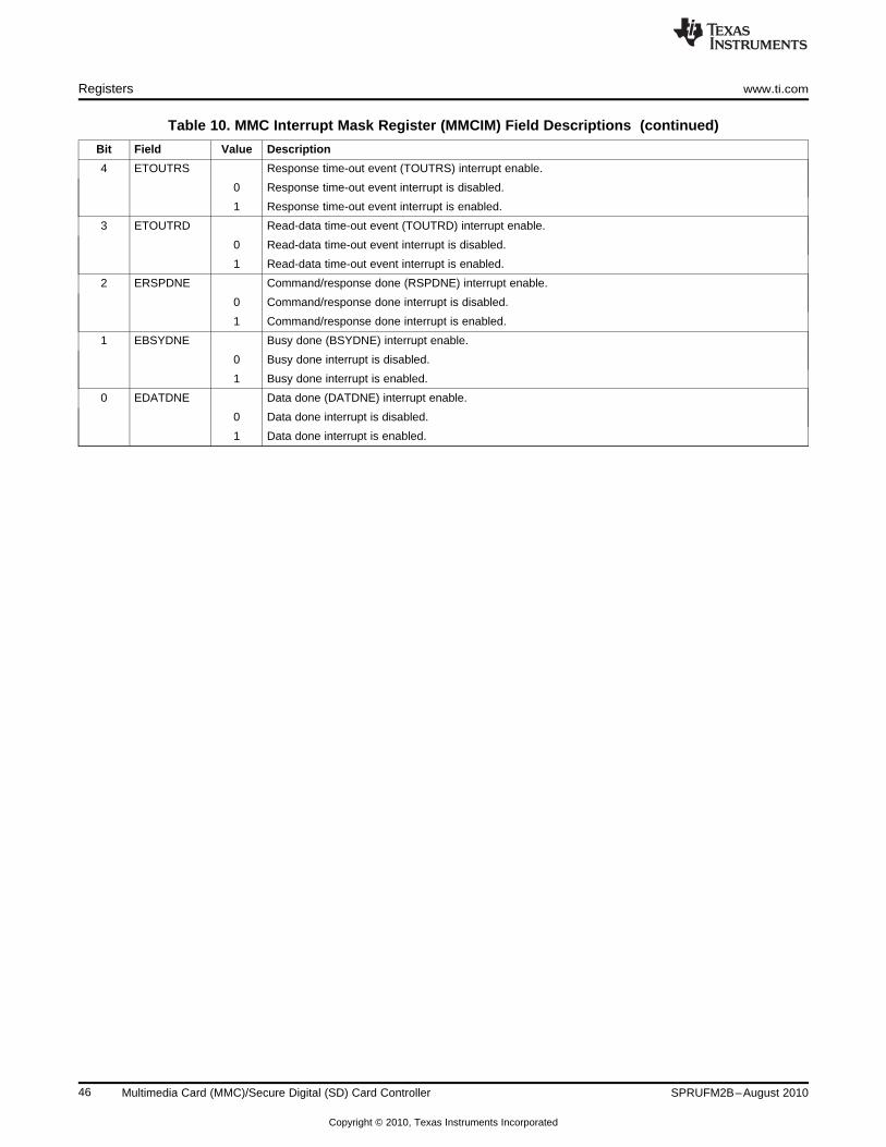
Registers www.ti.com
Table 10. MMC Interrupt Mask Register (MMCIM) Field Descriptions (continued)
Bit Field Value Description
4 ETOUTRS Response time-out event (TOUTRS) interrupt enable.
0 Response time-out event interrupt is disabled.
1 Response time-out event interrupt is enabled.
3 ETOUTRD Read-data time-out event (TOUTRD) interrupt enable.
0 Read-data time-out event interrupt is disabled.
1 Read-data time-out event interrupt is enabled.
2 ERSPDNE Command/response done (RSPDNE) interrupt enable.
0 Command/response done interrupt is disabled.
1 Command/response done interrupt is enabled.
1 EBSYDNE Busy done (BSYDNE) interrupt enable.
0 Busy done interrupt is disabled.
1 Busy done interrupt is enabled.
0 EDATDNE Data done (DATDNE) interrupt enable.
0 Data done interrupt is disabled.
1 Data done interrupt is enabled.
46 Multimedia Card (MMC)/Secure Digital (SD) Card Controller SPRUFM2B–August 2010
Copyright © 2010, Texas Instruments Incorporated

www.ti.com Registers
4.6 MMC Response Time-Out Register (MMCTOR)
The MMC response time-out register (MMCTOR) defines how long the MMC controller waits for aresponse from a memory card before recording a time-out condition in the TOUTRS bit of the MMC statusregister 0 (MMCST0). If the corresponding ETOUTRS bit in the MMC interrupt mask register (MMCIM) isset, an interrupt is generated when the TOUTRS bit is set in MMCST0. If a memory card should require alonger time-out period than MMCTOR can provide, a software time-out mechanism can be implemented.
The MMC response time-out register (MMCTOR) is shown in Figure 22 and described in Table 11.
Figure 22. MMC Response Time-Out Register (MMCTOR)31 18 17 16
Reserved TOD_25_16
R-0 R/W-0
15 8 7 0
TOD_25_16 TOR
R/W-0 R/W-0
LEGEND: R/W = Read/Write; R = Read only; -n = value after reset
Table 11. MMC Response Time-Out Register (MMCTOR) Field Descriptions
Bit Field Value Description
31-18 Reserved 0 Reserved
17-8 TOD_25_16 0-3FFh Data read time-out count upper 10 bits. Used in conjunction with the TOD_15_0 bits inMMCTOD to form a 26-bit count (1 CLK clock cycle to 67 108 863 CLK clock cycles). SeeMMCTOD (Section 4.7).
0 No time out
1h-3FF FFFFh 1 CLK clock cycle to 67 108 863 CLK clock cycles
7-0 TOR 0-FFh Time-out count for response.
0 No time out
1h-FFh 1 CLK clock cycle to 255 CLK clock cycles
47SPRUFM2B–August 2010 Multimedia Card (MMC)/Secure Digital (SD) Card Controller
Copyright © 2010, Texas Instruments Incorporated

Registers www.ti.com
4.7 MMC Data Read Time-Out Register (MMCTOD)
The MMC data read time-out register (MMCTOD) defines how long the MMC controller waits for the datafrom a memory card before recording a time-out condition in the TOUTRD bit of the MMC status register 0(MMCST0). If the corresponding ETOUTRD bit in the MMC interrupt mask register (MMCIM) is set, aninterrupt is generated when the TOUTRD bit is set in MMCST0. If a memory card should require a longertime-out period than MMCTOD can provide, a software time-out mechanism can be implemented.
The MMC data read time-out register (MMCTOD) is shown in Figure 23 and described in Table 12.
Figure 23. MMC Data Read Time-Out Register (MMCTOD)31 16
Reserved
R-0
15 0
TOD_15_0
R/W-0
LEGEND: R/W = Read/Write; R = Read only; -n = value after reset
Table 12. MMC Data Read Time-Out Register (MMCTOD) Field Descriptions
Bit Field Value Description
31-16 Reserved 0 Reserved
15-0 TOD_15_0 0-FFFFh Data read time-out count. Used in conjunction with the TOD_25_16 bits in MMCTOR toform a 26-bit count (1 CLK clock cycle to 67 108 863 CLK clock cycles). See MMCTOR(Section 4.6).
0 No time out
1h-3FF FFFFh 1 CLK clock cycle to 67 108 863 CLK clock cycles
48 Multimedia Card (MMC)/Secure Digital (SD) Card Controller SPRUFM2B–August 2010
Copyright © 2010, Texas Instruments Incorporated

www.ti.com Registers
4.8 MMC Block Length Register (MMCBLEN)
The MMC block length register (MMCBLEN) specifies the data block length in bytes. This value mustmatch the block length setting in the memory card.
The MMC block length register (MMCBLEN) is shown in Figure 24 and described in Table 13.
NOTE: The BLEN bits value must be the same as the CSD register settings in the MMC/SD card.To be precise, it should match the value of the READ_BL_LEN field for read, orWRITE_BL_LEN field for write.
Figure 24. MMC Block Length Register (MMCBLEN)31 16
Reserved
R-0
15 12 11 0
Reserved BLEN
R-0 R/W-200h
LEGEND: R/W = Read/Write; R = Read only; -n = value after reset
Table 13. MMC Block Length Register (MMCBLEN) Field Descriptions
Bit Field Value Description
31-12 Reserved 0 Reserved
11−0 BLEN 1h−FFFh Block length. This field is used to set the block length, which is the byte count of a data block. Thevalue 0 is prohibited.
49SPRUFM2B–August 2010 Multimedia Card (MMC)/Secure Digital (SD) Card Controller
Copyright © 2010, Texas Instruments Incorporated

Registers www.ti.com
4.9 MMC Number of Blocks Register (MMCNBLK)
The MMC number of blocks register (MMCNBLK) specifies the number of blocks for a multiple-blocktransfer.
The MMC number of blocks register (MMCNBLK) is shown in Figure 25 and described in Table 14.
Figure 25. MMC Number of Blocks Register (MMCNBLK)31 16
Reserved
R-0
15 0
NBLK
R/W-0
LEGEND: R/W = Read/Write; R = Read only; -n = value after reset
Table 14. MMC Number of Blocks Register (MMCNBLK) Field Descriptions
Bit Field Value Description
31-16 Reserved 0 Reserved
15-0 NBLK 0-FFFFh Number of blocks. This field is used to set the total number of blocks to be transferred.
0 Infinite number of blocks. The MMC controller reads/writes blocks of data until aSTOP_TRANSMISSION command is written to the MMC command register (MMCCMD).
1h−FFFFh n blocks. The MMC controller reads/writes only n blocks of data, even if theSTOP_TRANSMISSION command has not been written to the MMC command register(MMCCMD).
4.10 MMC Number of Blocks Counter Register (MMCNBLC)
The MMC number of blocks counter register (MMCNBLC) is a down-counter for tracking the number ofblocks remaining to be transferred during a multiple-block transfer.
The MMC number of blocks counter register (MMCNBLC) is shown in Figure 26 and described inTable 15.
Figure 26. MMC Number of Blocks Counter Register (MMCNBLC)31 16
Reserved
R-0
15 0
NBLC
R-FFFFh
LEGEND: R/W = Read/Write; R = Read only; -n = value after reset
Table 15. MMC Number of Blocks Counter Register (MMCNBLC) Field Descriptions
Bit Field Value Description
31-16 Reserved 0 Reserved
15-0 NBLC 0−FFFFh Read this field to determine the number of blocks remaining to be transferred.
50 Multimedia Card (MMC)/Secure Digital (SD) Card Controller SPRUFM2B–August 2010
Copyright © 2010, Texas Instruments Incorporated

www.ti.com Registers
4.11 MMC Data Receive Register (MMCDRR)
The MMC data receive register (MMCDRR) is used for storing the received data from the MMC controller.The CPU or the DMA controller can read data from this register. MMCDRR expects the data inlittle-endian format.
The MMC data receive register (MMCDRR) is shown in Figure 27 and described in Table 16.
Figure 27. MMC Data Receive Register (MMCDRR)31 0
DRR
R/W-0
LEGEND: R/W = Read/Write; -n = value after reset
Table 16. MMC Data Receive Register (MMCDRR) Field Descriptions
Bit Field Value Description
31-0 DRR 0-FFFF FFFFh Data receive.
4.12 MMC Data Transmit Register (MMCDXR)
The MMC data transmit register (MMCDXR) is used for storing the data to be transmitted from the MMCcontroller to the memory card. The CPU or the DMA controller can write data to this register to betransmitted. MMCDXR expects the data in little-endian format.
The MMC data transmit register (MMCDXR) is shown in Figure 28 and described in Table 17.
Figure 28. MMC Data Transmit Register (MMCDXR)31 0
DXR
R/W-0
LEGEND: R/W = Read/Write; -n = value after reset
Table 17. MMC Data Transmit Register (MMCDXR) Field Descriptions
Bit Field Value Description
31-0 DXR 0-FFFF FFFFh Data transmit.
51SPRUFM2B–August 2010 Multimedia Card (MMC)/Secure Digital (SD) Card Controller
Copyright © 2010, Texas Instruments Incorporated

Registers www.ti.com
4.13 MMC Command Register (MMCCMD)
NOTE: Writing to the MMC command register (MMCCMD) causes the MMC controller to send theprogrammed command. Therefore, the MMC argument register (MMCARGHL) must beloaded properly before a write to MMCCMD.
The MMC command register (MMCCMD) specifies the type of command to be sent and defines theoperation (command, response, additional activity) for the MMC controller. The content of MMCCMD iskept after the transfer to the transmit shift register. The MMC command register (MMCCMD) is shown inFigure 29 and described in Table 18.
When the CPU writes to MMCCMD, the MMC controller sends the programmed command, including anyarguments in the MMC argument register (MMCARGHL). For the format of a command (index, arguments,and other bits), see Figure 30 and Table 19.
Figure 29. MMC Command Register (MMCCMD)31 24
Reserved
R-0
23 17 16
Reserved DMATRIG
R-0 R/W-0
15 14 13 12 11 10 9 8
DCLR INITCK WDATX STRMTP DTRW RSPFMT BSYEXP
R/W-0 R/W-0 R/W-0 R/W-0 R/W-0 R/W-0 R/W-0
7 6 5 0
PPLEN Reserved CMD
R/W-0 R-0 R/W-0
LEGEND: R/W = Read/Write; R = Read only; -n = value after reset
Table 18. MMC Command Register (MMCCMD) Field Descriptions
Bit Field Value Description
31-17 Reserved 0 Reserved
16 DMATRIG Data transfer triggering. (Read back as 0.)
0 Data transfer has not been triggered.
1 Data transfer is triggered.
15 DCLR Data receive/transmit clear. Use this bit to clear the data receive ready (DRRDY) bit and the datatransmit ready (DXRDY) bit in the MMC status register 0 (MMCST0) before a new read or writesequence. This clears any previous status.
0 Do not clear DRRDY and DXRDY bits in MMCST0.
1 Clear DRRDY and DXRDY bits in MMCST0.
14 INITCK Initialization clock cycles.
0 Do not insert initialization clock cycles.
1 Insert initialization clock cycles; insert 80 CLK cycles before sending the command specified in the CMDbits. These dummy clock cycles are required for resetting a card after power on.
13 WDATX Data transfer indicator.
0 There is no data transfer.
1 There is a data transfer associated with the command.
52 Multimedia Card (MMC)/Secure Digital (SD) Card Controller SPRUFM2B–August 2010
Copyright © 2010, Texas Instruments Incorporated

www.ti.com Registers
Table 18. MMC Command Register (MMCCMD) Field Descriptions (continued)
Bit Field Value Description
12 STRMTP Stream enable.
0 If WDATX = 1, the data transfer is a block transfer. The data transfer stops after the movement of theprogrammed number of bytes (defined by the programmed block size and the programmed number ofblocks).
1 If WDATX = 1, the data transfer is a stream transfer. Once the data transfer is started, the data transferdoes not stop until the MMC controller issues a stop command to the memory card.
11 DTRW Write enable.
0 If WDATX = 1, the data transfer is a read operation.
1 If WDATX = 1, the data transfer is a write operation.
10-9 RSPFMT 0-3h Response format (expected type of response to the command).
0 No response.
1h R1, R4, R5, or R6 response. 48 bits with CRC.
2h R2 response. 136 bits with CRC.
3h R3 response. 48 bits with no CRC.
8 BSYEXP Busy expected. If an R1b (R1 with busy) response is expected, set RSPFMT = 1h and BSYEXP = 1.
0 A busy signal is not expected.
1 A busy signal is expected.
7 PPLEN Push pull enable.
0 Push pull driver of CMD line is disabled (open drain).
1 Push pull driver of CMD line is enabled.
6 Reserved 0 Reserved.
5-0 CMD 0-3Fh Command index. This field contains the command index for the command to be sent to the memorycard.
Figure 30. Command Format47 46 45 40 39 24
Start Transmission Command index Argument, high part
23 8 7 1 0
Argument, low part CRC7 End
Table 19. Command Format
Bit Positionof Command Register Description
47 - Start bit
46 - Transmission bit
45-40 MMCCMD(5-0) Command index (CMD)
39-24 MMCARGHL Argument, high part (ARGH)
23-8 MMCARGHL Argument, low part (ARGL)
7-1 - CRC7
0 - End bit
53SPRUFM2B–August 2010 Multimedia Card (MMC)/Secure Digital (SD) Card Controller
Copyright © 2010, Texas Instruments Incorporated

Registers www.ti.com
4.14 MMC Argument Register (MMCARGHL)
NOTE: Do not modify the MMC argument register (MMCARGHL) while it is being used for anoperation.
The MMC argument register (MMCARGHL) specifies the arguments to be sent with the commandspecified in the MMC command register (MMCCMD). Writing to MMCCMD causes the MMC controller tosend a command; therefore, MMCARGHL must be configured before writing to MMCCMD. The content ofMMCARGHL is kept after the transfer to the shift register; however, modification to MMCARGHL is notallowed during a sending operation. For the format of a command, see Figure 30 and Table 19.
The MMC argument register (MMCARGHL) is shown in Figure 31 and described in Table 20.
Figure 31. MMC Argument Register (MMCARGHL)31 16
ARGH
R/W-0
15 0
ARGL
R/W-0
LEGEND: R/W = Read/Write; -n = value after reset
Table 20. MMC Argument Register (MMCARGHL) Field Descriptions
Bit Field Value Description
31-16 ARGH 0-FFFFh Argument, high part.
15-0 ARGL 0-FFFFh Argument, low part.
54 Multimedia Card (MMC)/Secure Digital (SD) Card Controller SPRUFM2B–August 2010
Copyright © 2010, Texas Instruments Incorporated

www.ti.com Registers
4.15 MMC Response Registers (MMCRSP0-MMCRSP7)
Each command has a preset response type. When the MMC controller receives a response, it is stored insome or all of the eight MMC response registers (MMCRSP7-MMCRSP0). The response registers areupdated as the responses arrive, even if the CPU has not read the previous contents.
As shown in Figure 32, Figure 33, Figure 34, and Figure 35 each of the MMC response registers holds upto 16 bits. Table 21 and Table 22 show the format for each type of response and which MMC responseregisters are used for the bits of the response. The first byte of the response is a command index byte andis stored in the MMC command index register (MMCCIDX).
Figure 32. MMC Response Register 0 and 1 (MMCRSP01)31 16
MMCRSP1
R/W-0
15 0
MMCRSP0
R/W-0
LEGEND: R/W = Read/Write; -n = value after reset
Figure 33. MMC Response Register 2 and 3 (MMCRSP23)31 16
MMCRSP3
R/W-0
15 0
MMCRSP2
R/W-0
LEGEND: R/W = Read/Write; -n = value after reset
Figure 34. MMC Response Register 4 and 5 (MMCRSP45)31 16
MMCRSP5
R/W-0
15 0
MMCRSP4
R/W-0
LEGEND: R/W = Read/Write; -n = value after reset
Figure 35. MMC Response Register 6 and 7 (MMCRSP67)31 16
MMCRSP7
R/W-0
15 0
MMCRSP6
R/W-0
LEGEND: R/W = Read/Write; -n = value after reset
55SPRUFM2B–August 2010 Multimedia Card (MMC)/Secure Digital (SD) Card Controller
Copyright © 2010, Texas Instruments Incorporated

Registers www.ti.com
Table 21. R1, R3, R4, R5, or R6 Response (48 Bits)
Bit Position of Response Register
47-40 MMCCIDX
39-24 MMCRSP7
23-8 MMCRSP6
7-0 MMCRSP5 (1)
- MMCRSP4-0(1) Bits 7-0 of the response are stored to bits 7-0 of MMCRSP5.
Table 22. R2 Response (136 Bits)
Bit Position of Response Register
135-128 MMCCIDX
127-112 MMCRSP7
111-96 MMCRSP6
95-80 MMCRSP5
79-64 MMCRSP4
63-48 MMCRSP3
47-32 MMCRSP2
31-16 MMCRSP1
15-0 MMCRSP0
56 Multimedia Card (MMC)/Secure Digital (SD) Card Controller SPRUFM2B–August 2010
Copyright © 2010, Texas Instruments Incorporated

www.ti.com Registers
4.16 MMC Data Response Register (MMCDRSP)
After the MMC controller sends a data block to a memory card, the return byte from the memory card isstored in the MMC data response register (MMCDRSP).
The MMC data response register (MMCDRSP) is shown in Figure 36 and described in Table 23.
Figure 36. MMC Data Response Register (MMCDRSP)31 16
Reserved
R-0
15 8 7 0
Reserved DRSP
R-0 R/W-0
LEGEND: R/W = Read/Write; R = Read only; -n = value after reset
Table 23. MMC Data Response Register (MMCDRSP) Field Descriptions
Bit Field Value Description
31-8 Reserved 0 Reserved
7-0 DRSP 0-FFh During a write operation (see Section 2.3.1), the CRC status token is stored in DRSP.
4.17 MMC Command Index Register (MMCCIDX)
The MMC command index register (MMCCIDX) stores the first byte of a response from a memory card.Table 21 and Table 22 show the format for each type of response.
The MMC command index register (MMCCIDX) is shown in Figure 37 and described in Table 24.
Figure 37. MMC Command Index Register (MMCCIDX)31 16
Reserved
R-0
15 8 7 6 5 0
Reserved STRT XMIT CIDX
R-0 R/W-0 R/W-0 R/W-0
LEGEND: R/W = Read/Write; R = Read only; -n = value after reset
Table 24. MMC Command Index Register (MMCCIDX) Field Descriptions
Bit Field Value Description
31-8 Reserved 0 Reserved
7 STRT 0-1 Start bit. When the MMC controller receives a response, the start bit is stored in STRT.
6 XMIT 0-1 Transmission bit. When the MMC controller receives a response, the transmission bit is stored in XMIT.
5-0 CIDX 0-3Fh Command index. When the MMC controller receives a response, the command index is stored in CIDX.
57SPRUFM2B–August 2010 Multimedia Card (MMC)/Secure Digital (SD) Card Controller
Copyright © 2010, Texas Instruments Incorporated

Registers www.ti.com
4.18 SDIO Control Register (SDIOCTL)
The SDIO control register (SDIOCTL) is shown in Figure 38 and described in Table 25.
Figure 38. SDIO Control Register (SDIOCTL)31 16
Reserved
R-0
15 2 1 0
Reserved RDWTCR RDWTRQ
R-0 R/W-0 R/W-0
LEGEND: R/W = Read/Write; R = Read only; -n = value after reset
Table 25. SDIO Control Register (SDIOCTL) Field Descriptions
Bit Field Value Description
31-2 Reserved 0 Reserved
1 RDWTCR Read wait enable for CRC error. To end the read wait operation, write 0 to RDWTRQ. (No need to clearRDWTCR).
0 Read wait is disabled.
1 Automatically start read wait on CRC error detection during multiple block read access and not the lastblock to be transferred. RDWTRQ is automatically set to 1.
0 RDWTRQ Read wait request. To end the read wait operation, write 0 to RDWTRQ.
0 End read wait operation and release MMCSD_DAT2.
1 Set a read wait request. Read wait operation starts 2 clocks after the end of the read data block.MMCIF asserts low level on MMCSD_DAT2 until RDWTRQ is cleared to 0.
58 Multimedia Card (MMC)/Secure Digital (SD) Card Controller SPRUFM2B–August 2010
Copyright © 2010, Texas Instruments Incorporated

www.ti.com Registers
4.19 SDIO Status Register 0 (SDIOST0)
The SDIO status register 0 (SDIOST0) is shown in Figure 39 and described in Table 26.
Figure 39. SDIO Status Register 0 (SDIOST0)31 16
Reserved
R-0
15 3 2 1 0
Reserved RDWTST INTPRD DAT1
R-0 R-0 R-0 R-1
LEGEND: R/W = Read/Write; R = Read only; -n = value after reset
Table 26. SDIO Status Register 0 (SDIOST0) Field Descriptions
Bit Field Value Description
31-3 Reserved 0 Reserved
2 RDWTST Read wait status.
0 Read wait operation not in progress.
1 Read wait operation in progress.
1 INTPRD Interrupt period.
0 Interrupt not in progress.
1 Interrupt in progress.
0 DAT1 This bit reflects the external state of the SD_DATA1 pin.
0 Logic-low level on the SD_DATA1 pin.
1 Logic-high level on the SD_DATA1 pin.
59SPRUFM2B–August 2010 Multimedia Card (MMC)/Secure Digital (SD) Card Controller
Copyright © 2010, Texas Instruments Incorporated

Registers www.ti.com
4.20 SDIO Interrupt Enable Register (SDIOIEN)
The SDIO interrupt enable register (SDIOIEN) is shown in Figure 40 and described in Table 27.
Figure 40. SDIO Interrupt Enable Register (SDIOIEN)31 16
Reserved
R-0
15 2 1 0
Reserved RWSEN IOINTEN
R-0 R/W-0 R/W-0
LEGEND: R/W = Read/Write; R = Read only; -n = value after reset
Table 27. SDIO Interrupt Enable Register (SDIOIEN) Field Descriptions
Bit Field Value Description
31-2 Reserved 0 Reserved
1 RWSEN Read wait interrupt enable.
0 Read wait interrupt is disabled.
1 Read wait interrupt is enabled.
0 IOINTEN SDIO card interrupt enable.
0 SDIO card interrupt is disabled.
1 SDIO card interrupt is enabled.
4.21 SDIO Interrupt Status Register (SDIOIST)
The SDIO interrupt status register (SDIOIST) is shown in Figure 41 and described in Table 28.
Figure 41. SDIO Interrupt Status Register (SDIOIST)31 16
Reserved
R-0
15 2 1 0
Reserved RWS IOINT
R-0 R/W1C-0 R/W1C-0
LEGEND: R/W = Read/Write; R = Read only; W1C = Write 1 to clear (writing 0 has no effect); -n = value after reset
Table 28. SDIO Interrupt Status Register (SDIOIST) Field Descriptions
Bit Field Value Description
31-2 Reserved 0 Reserved
1 RWS Read wait interrupt status. Write a 1 to clear this bit.
0 Read wait interrupt did not occur.
1 Read wait interrupt occurred. Read wait operation starts and read wait interrupt is enabled(RWSEN = 1 in SDIOIEN).
0 IOINT SDIO card interrupt status. Write a 1 to clear this bit.
0 SDIO card interrupt did not occur.
1 SDIO card interrupt occurred. SDIO card interrupt is detected and SDIO card interrupt is enabled(IOINTEN = 1 in SDIOIEN).
60 Multimedia Card (MMC)/Secure Digital (SD) Card Controller SPRUFM2B–August 2010
Copyright © 2010, Texas Instruments Incorporated

www.ti.com Registers
4.22 MMC FIFO Control Register (MMCFIFOCTL)
The MMC FIFO control register (MMCFIFOCTL) is shown in Figure 42 and described in Table 29.
Figure 42. MMC FIFO Control Register (MMCFIFOCTL)31 16
Reserved
R-0
15 5 4 3 2 1 0
Reserved ACCWD FIFOLEV FIFODIR FIFORST
R-0 R/W-0 R/W-0 R/W-0 R/W-0
LEGEND: R/W = Read/Write; R = Read only; -n = value after reset
Table 29. MMC FIFO Control Register (MMCFIFOCTL) Field Descriptions
Bit Field Value Description
31-5 Reserved 0 Reserved
4-3 ACCWD 0-3h Access width. Used by FIFO control to determine full/empty flag.
0 CPU/EDMA access width of 4 bytes.
1h CPU/EDMA access width of 3 bytes.
2h CPU/EDMA access width of 2 bytes.
3h CPU/EDMA access width of 1 byte.
2 FIFOLEV FIFO level. Sets the threshold level that determines when the EDMA request and the FIFO thresholdinterrupt are triggered.
0 EDMA request every 256 bits (32 bytes) sent/received.
1 EDMA request every 512 bits (64 bytes) sent/received.
1 FIFODIR FIFO direction. Determines if the FIFO is being written to or read from.
0 Read from FIFO.
1 Write to FIFO.
0 FIFORST FIFO reset. Resets the internal state of the FIFO.
0 FIFO reset is disabled.
1 FIFO reset is enabled.
61SPRUFM2B–August 2010 Multimedia Card (MMC)/Secure Digital (SD) Card Controller
Copyright © 2010, Texas Instruments Incorporated

www.ti.com
Appendix A Revision History
Table 30 lists the changes made since the previous version of this document.
Table 30. Document Revision History
Reference Additions/Modifications/Deletions
Section 1.5 Changed first and third bullets.
62 Revision History SPRUFM2B–August 2010
Copyright © 2010, Texas Instruments Incorporated

IMPORTANT NOTICE
Texas Instruments Incorporated and its subsidiaries (TI) reserve the right to make corrections, modifications, enhancements, improvements,and other changes to its products and services at any time and to discontinue any product or service without notice. Customers shouldobtain the latest relevant information before placing orders and should verify that such information is current and complete. All products aresold subject to TI’s terms and conditions of sale supplied at the time of order acknowledgment.
TI warrants performance of its hardware products to the specifications applicable at the time of sale in accordance with TI’s standardwarranty. Testing and other quality control techniques are used to the extent TI deems necessary to support this warranty. Except wheremandated by government requirements, testing of all parameters of each product is not necessarily performed.
TI assumes no liability for applications assistance or customer product design. Customers are responsible for their products andapplications using TI components. To minimize the risks associated with customer products and applications, customers should provideadequate design and operating safeguards.
TI does not warrant or represent that any license, either express or implied, is granted under any TI patent right, copyright, mask work right,or other TI intellectual property right relating to any combination, machine, or process in which TI products or services are used. Informationpublished by TI regarding third-party products or services does not constitute a license from TI to use such products or services or awarranty or endorsement thereof. Use of such information may require a license from a third party under the patents or other intellectualproperty of the third party, or a license from TI under the patents or other intellectual property of TI.
Reproduction of TI information in TI data books or data sheets is permissible only if reproduction is without alteration and is accompaniedby all associated warranties, conditions, limitations, and notices. Reproduction of this information with alteration is an unfair and deceptivebusiness practice. TI is not responsible or liable for such altered documentation. Information of third parties may be subject to additionalrestrictions.
Resale of TI products or services with statements different from or beyond the parameters stated by TI for that product or service voids allexpress and any implied warranties for the associated TI product or service and is an unfair and deceptive business practice. TI is notresponsible or liable for any such statements.
TI products are not authorized for use in safety-critical applications (such as life support) where a failure of the TI product would reasonablybe expected to cause severe personal injury or death, unless officers of the parties have executed an agreement specifically governingsuch use. Buyers represent that they have all necessary expertise in the safety and regulatory ramifications of their applications, andacknowledge and agree that they are solely responsible for all legal, regulatory and safety-related requirements concerning their productsand any use of TI products in such safety-critical applications, notwithstanding any applications-related information or support that may beprovided by TI. Further, Buyers must fully indemnify TI and its representatives against any damages arising out of the use of TI products insuch safety-critical applications.
TI products are neither designed nor intended for use in military/aerospace applications or environments unless the TI products arespecifically designated by TI as military-grade or "enhanced plastic." Only products designated by TI as military-grade meet militaryspecifications. Buyers acknowledge and agree that any such use of TI products which TI has not designated as military-grade is solely atthe Buyer's risk, and that they are solely responsible for compliance with all legal and regulatory requirements in connection with such use.
TI products are neither designed nor intended for use in automotive applications or environments unless the specific TI products aredesignated by TI as compliant with ISO/TS 16949 requirements. Buyers acknowledge and agree that, if they use any non-designatedproducts in automotive applications, TI will not be responsible for any failure to meet such requirements.
Following are URLs where you can obtain information on other Texas Instruments products and application solutions:
Products Applications
Amplifiers amplifier.ti.com Audio www.ti.com/audio
Data Converters dataconverter.ti.com Automotive www.ti.com/automotive
DLP® Products www.dlp.com Communications and www.ti.com/communicationsTelecom
DSP dsp.ti.com Computers and www.ti.com/computersPeripherals
Clocks and Timers www.ti.com/clocks Consumer Electronics www.ti.com/consumer-apps
Interface interface.ti.com Energy www.ti.com/energy
Logic logic.ti.com Industrial www.ti.com/industrial
Power Mgmt power.ti.com Medical www.ti.com/medical
Microcontrollers microcontroller.ti.com Security www.ti.com/security
RFID www.ti-rfid.com Space, Avionics & www.ti.com/space-avionics-defenseDefense
RF/IF and ZigBee® Solutions www.ti.com/lprf Video and Imaging www.ti.com/video
Wireless www.ti.com/wireless-apps
Mailing Address: Texas Instruments, Post Office Box 655303, Dallas, Texas 75265Copyright © 2010, Texas Instruments Incorporated