title : hv121x02-100 product specification · this specification is the property of boe hydis and...
TRANSCRIPT

PROPRIETARY NOTE THIS SPECIFICATION IS THE PROPERTY OF BOE HYDIS AND SHALL NOT BE REPRODUCED OR COPIED WITHOUT THE WRITTEN PERMISSION OF BOE HYDIS AND MUST BE RETURNED TO BOE HYDIS UPON ITS REQUEST.
TITLE : HV121X02-100 Product Specification
Rev. O
BOE HYDIS TECHNOLOGY
SPEC. NUMBER S864-1266
PRODUCT GROUP TFT-LCD PRODUCT
REV. O
ISSUE DATE 2006.01.25
PAGE 1 OF 22
B2005-C001-A (1/3) A4(210 X 297)

PRODUCT GROUP REV. ISSUE DATE
TFT-LCD PRODUCT O 2006.01.25
REVISION HISTORYREV. ECN NO. DESCRIPTION OF CHANGES DATE PREPARED
O - Initial Release 06.01.25 J.K.Han
PAGE SPEC. NUMBER
S864-1266 SPEC. TITLE
HV121X02-100 Product Specification 2 OF 22
B2005-C001-A (2/3) A4(210 X 297)

PRODUCT GROUP REV. ISSUE DATE
TFT-LCD PRODUCT O 2006.01.25
PAGE SPEC. NUMBER S864-1266
SPEC. TITLE HV121X02-100 Product Specification
3 OF 22
B2005-C001-A (3/3) A4(210 X 297)
Contents
No Item Page
1.0 General Description 4
2.0 Environmental absolute maximum ratings 5
3.0 Optical specifications 6
4.0 Electrical specifications 7
5.0 Interface connection 8
6.0 Signal timing specifications 9
7.0 Signal timing waveforms of interface signal 11
8.0 Input signals, basic display colors & gray scale of colors 12
9.0 Power sequence 13
10.0 Reliability test 14
11.0 Handling & cautions 16
12.0 Appendix 17
PRODUCT GROUP REV. ISSUE DATE
TFT-LCD PRODUCT O 2006.01.25
PAGE SPEC. NUMBER S864-1266
SPEC. TITLE HV121X02-100 Product Specification
4 OF 22
B2005-C001-A (3/3) A4(210 X 297)
1.0 GENERAL DESCRIPTION
1.1 Introduction
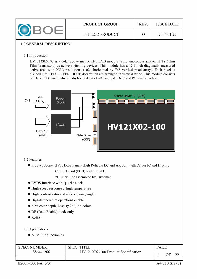
HV121X02-100 is a color active matrix TFT LCD module using amorphous silicon TFT's (Thin Film Transistors) as active switching devices. This module has a 12.1 inch diagonally measured active area with XGA resolutions (1024 horizontal by 768 vertical pixel array). Each pixel is divided into RED, GREEN, BLUE dots which are arranged in vertical stripe. This module consists of TFT-LCD panel, which Tabs bonded data D-IC and gate D-IC and PCB are attached.
1.2 Features
z Product Scope: HV121X02 Panel (High Reliable LC and AR pol.) with Driver IC and Driving
Circuit Board (PCB) without BLU
*BLU will be assembled by Customer.
z LVDS Interface with 1pixel / clock
z High-speed response at high temperature
z High contrast ratio and wide viewing angle
z High-temperature operations enable
z 6-bit color depth, Display 262,144 colors
z DE (Data Enable) mode only
z RoHS
1.3 Applications
z ATM / Car / Avionics
HV121X02-100 {Vjvu
LVDS 1CH (6bit)
w����G
i���� VDD
(3.3V) CN1Source Driver IC (COF)
Gate Driver IC(COF)
PRODUCT GROUP REV. ISSUE DATE
TFT-LCD PRODUCT O 2006.01.25
PAGE SPEC. NUMBER S864-1266
SPEC. TITLE HV121X02-100 Product Specification
5 OF 22
B2005-C001-A (3/3) A4(210 X 297)
1.4 General Specifications
The followings are general specifications at the model HV121X02-100.
Parameter Specification Unit Remark
Active area 245.76 (H) Ý 184.32 (V) mm
Number of pixels 1024(H) ϧ 768(V) pixels
Pixel pitch 0.24(H) ϧ 0.24(V) mm
Pixel arrangement RGB Vertical stripe -
Display mode Normally Black (FFS) -
Surface treatment Anti-Reflective (No Haze) -
Liquid Crystal clearing temperature
103 ఁ
Color filter Chromaticity x=0.312, y=0.342
CF Color Gamut 40 %
Panel Transmittance 5.91
(excluding the gain of the rear-polarizer)% Note. 1
Note 1) The Panel Transmittance as described above, will be obtained after electronics and back-light driving circuit are optimized to a panel.
2.0 ENVIRONMENTAL ABSOLUTE MAXIMUM RATINGS
The followings are maximum values which, if exceed, may cause faulty operation or damage to the unit.
Parameter Symbol Min Max Unit Remark
Operating Temperature TOP -20 +85 ଇ Note. 1
Note. 1) As compromised with Customer, T-CON, D-IC, Polarizer are excluded within the range
of guarantee for Operating Temperature. T-CON : 0 ~ 75ଇ, D-IC : -10 ~ 75ଇ, Polarizer : -20 ~ 80ଇ

PRODUCT GROUP REV. ISSUE DATE
TFT-LCD PRODUCT O 2006.01.25
PAGE SPEC. NUMBER S864-1266
SPEC. TITLE HV121X02-100 Product Specification
6 OF 22
B2005-C001-A (3/3) A4(210 X 297)
3.0 OPTICAL SPECIFICATIONS
3.1 Overview The test of Optical specifications shall be measured in a dark room (ambient luminance d 1 lux and temperature = 25r2ఁ) with the equipment of Luminance meter system (Goniometer system and TOPCON BM-5) and test unit shall be located at an approximate distance 50cm from the LCD surface at a viewing angle of T and I equal to 0q. We refer to TI=0 (=T3) as the 3 o’clock direction (the “right”), TI=90 (=T12) as the 12 o’clock direction (“upward”), TI=180 (=T9) as the 9 o’clock direction (“left”) and TI=270 (=T6) as the 6 o’clock direction (“bottom”). While scanning T and/or I, the center of the measuring spot on the display surface shall stay fixed. The test setup, geometry, and measurement location are shown in FIGURE 1, and FIGURE 2. (shown in Appendix)
3.2 Optical Specifications The measurement shall be executed after 30 minutes warm-up period.
[VDD=3.3V, Frame rate=60Hz, Clock=65MHz, Ta = 25±2 ]ଇ
Parameter Symbol Condition Min Typ Max Unit Remark
ԭ 3 89 90 Deg Horizontal
ԭ 9 89 90 Deg
ԭ 12 89 90 Deg
Viewing
Angle Vertical
ԭ 6
CR > 10
89 90 Deg
Note 1
Luminance contrast ratio CR - 450 - Note 2
Color Reproduction 40 45 - %
Response time
(at 45ఁ)
Ttotal
(Tr + Td) Ttotal - - 32 msec Note 3
Cross talk CT
ԭ = 0q
(Center)
Normal
Viewing
Angle - - 2.0 % Note 4
Note:
1. Viewing angle is the angle at which the contrast ratio is greater than 10. The viewing are determined for the horizontal or 3, 9 o’clock direction and the vertical or 6, 12 o’clock direction with respect to the optical axis which is normal to the LCD surface (see FIGURE 1 shown in Appendix).
2. Contrast measurements shall be made at viewing angle of ԭ = 0q and at the center of the LCD surface. Luminance shall be measured with all pixels in the view field set first to white, then to the dark (black) state. (See FIGURE 1 shown in Appendix) Luminance Contrast Ratio (CR) is defined mathematically.

PRODUCT GROUP REV. ISSUE DATE
TFT-LCD PRODUCT O 2006.01.25
PAGE SPEC. NUMBER S864-1266
SPEC. TITLE HV121X02-100 Product Specification
7 OF 22
B2005-C001-A (3/3) A4(210 X 297)
Luminance when displaying a white raster CR =
Luminance when displaying a black raster
3. The electro-optical response time measurements shall be made as FIGURE 2 shown in Appendix by switching the “data” input signal ON and OFF. The times needed for the luminance to change from 10% to 90% is Tr, and 90% to 10% is Td.
4. Cross-Talk of one area of the LCD surface by another shall be measured by comparing the luminance (YA) of a 25mm diameter area, with all display pixels set to a gray level, to the luminance (YB) of that same area when any adjacent area is driven dark. (See FIGURE 3 shown in Appendix).
4.0 ELECTRICAL SPECIFICATIONS
[Ta = 25±2 ]ଇ
Parameter Min Typ Max Unit Remark
Power Supply Voltage VDD 3.0 3.3 3.6 V
Power Supply Current IDD - 220 mA Note1
Power Consumption PD 0.7 1.1 W
Permissible Input Ripple Voltage VRF - - 100 mV VDD = 3.3V
High Level Differential Input
Threshold Voltage VIH - - +100 mV
Low Level Differential Input
Threshold Voltage VIL -100 - - mV
Vcm
= 1.2V typ.
Notes:
1. The supply voltage is measured and specified at the interface connector of LCM.
The current draw and power consumption specified is for VDD = 3.3V, Frame rate = 60 Hz and Clock frequency = 65MHz. Test Pattern of power supply current
a) Typ: Vertical color bar pattern
b) Max : Gray 28 @ Vertical 2 Skip line pattern
PRODUCT GROUP REV. ISSUE DATE
TFT-LCD PRODUCT O 2006.01.25
PAGE SPEC. NUMBER S864-1266
SPEC. TITLE HV121X02-100 Product Specification
8 OF 22
B2005-C001-A (3/3) A4(210 X 297)
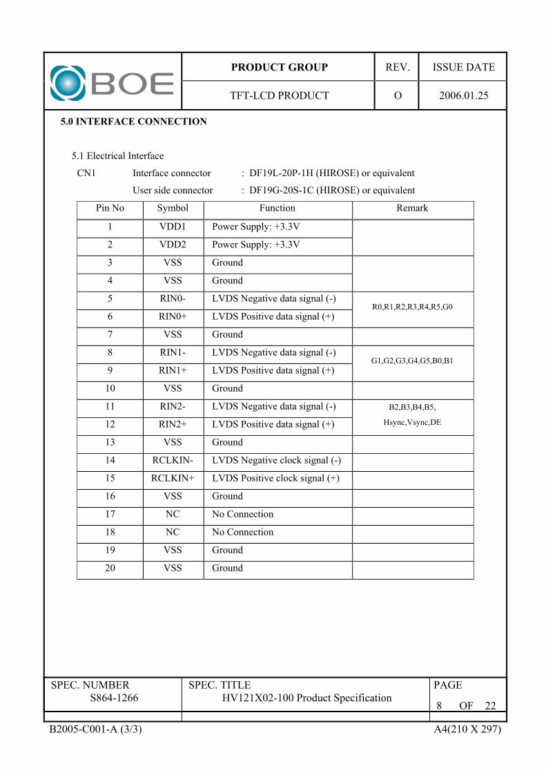
5.0 INTERFACE CONNECTION
5.1 Electrical Interface
CN1 Interface connector : DF19L-20P-1H (HIROSE) or equivalent
User side connector : DF19G-20S-1C (HIROSE) or equivalent
Pin No Symbol Function Remark
1 VDD1 Power Supply: +3.3V
2 VDD2 Power Supply: +3.3V
3 VSS Ground
4 VSS Ground
5 RIN0- LVDS Negative data signal (-)
6 RIN0+ LVDS Positive data signal (+) R0,R1,R2,R3,R4,R5,G0
7 VSS Ground
8 RIN1- LVDS Negative data signal (-)
9 RIN1+ LVDS Positive data signal (+) G1,G2,G3,G4,G5,B0,B1
10 VSS Ground
11 RIN2- LVDS Negative data signal (-)
12 RIN2+ LVDS Positive data signal (+)
B2,B3,B4,B5,
Hsync,Vsync,DE
13 VSS Ground
14 RCLKIN- LVDS Negative clock signal (-)
15 RCLKIN+ LVDS Positive clock signal (+)
16 VSS Ground
17 NC No Connection
18 NC No Connection
19 VSS Ground
20 VSS Ground
PRODUCT GROUP REV. ISSUE DATE
TFT-LCD PRODUCT O 2006.01.25
PAGE SPEC. NUMBER S864-1266
SPEC. TITLE HV121X02-100 Product Specification
9 OF 22
B2005-C001-A (3/3) A4(210 X 297)
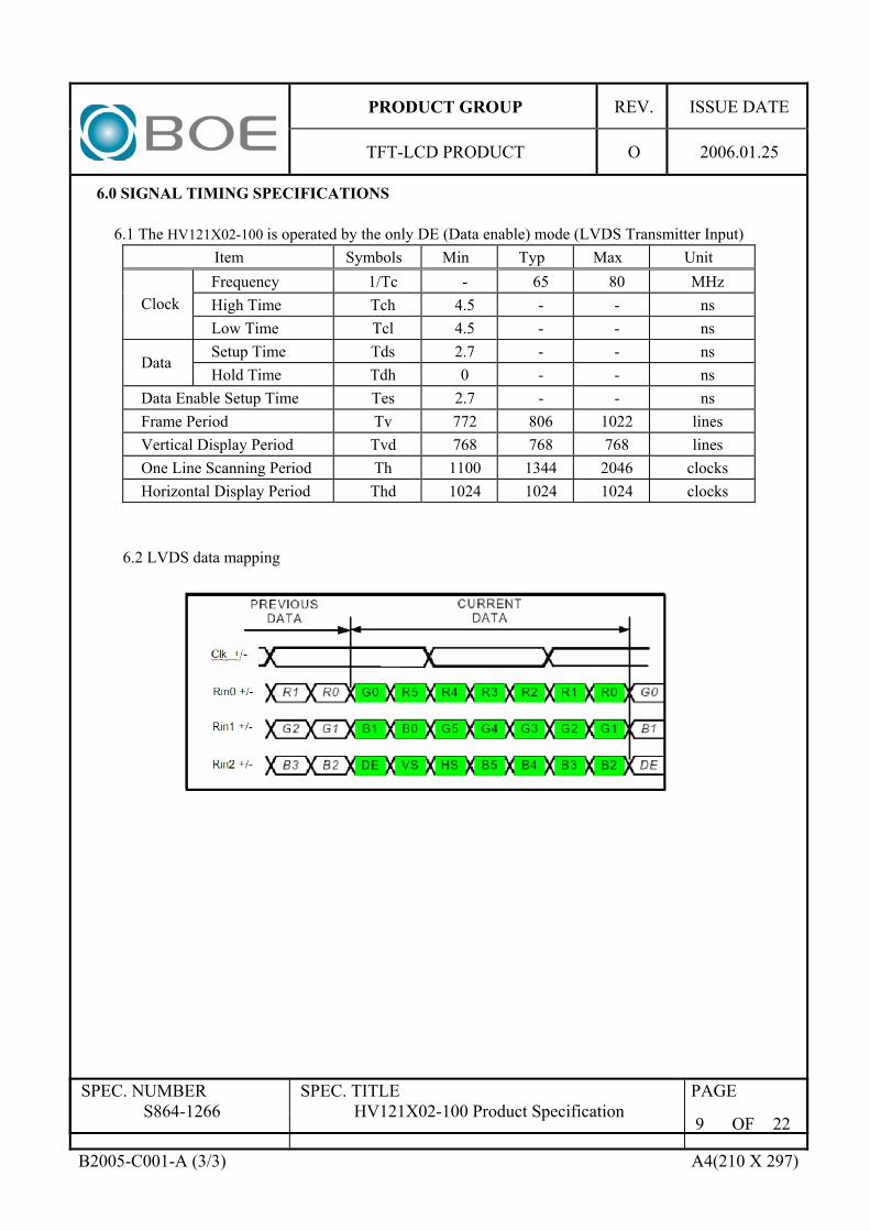
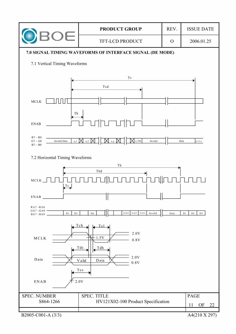
6.0 SIGNAL TIMING SPECIFICATIONS
6.1 The HV121X02-100 is operated by the only DE (Data enable) mode (LVDS Transmitter Input)
Item Symbols Min Typ Max Unit
Frequency 1/Tc - 65 80 MHz
High Time Tch 4.5 - - ns Clock
Low Time Tcl 4.5 - - ns
Setup Time Tds 2.7 - - ns Data
Hold Time Tdh 0 - - ns
Data Enable Setup Time Tes 2.7 - - ns
Frame Period Tv 772 806 1022 lines
Vertical Display Period Tvd 768 768 768 lines
One Line Scanning Period Th 1100 1344 2046 clocks
Horizontal Display Period Thd 1024 1024 1024 clocks
6.2 LVDS data mapping

PRODUCT GROUP REV. ISSUE DATE
TFT-LCD PRODUCT O 2006.01.25
PAGE SPEC. NUMBER S864-1266
SPEC. TITLE HV121X02-100 Product Specification
10 OF 22
B2005-C001-A (3/3) A4(210 X 297)
6.3 LVDS Rx interface timing parameter
The specification of the LVDS Rx interface timing parameter <LVDS Rx Interface Timing Specification>
Item Symbol Min Typ Max Unit Remark
CLKIN Period tRCIP 12.5 15.38 - nsec Input Data 0 tRIP1 -0.4 0.0 +0.4 nsec Input Data 1 tRIP0 1*tRICP/7
-0.4 1*tRICP/7 1*tRICP/7
+0.4 nsec
Input Data 2 tRIP6 2*tRICP/7 -0.4
2*tRICP/7 2*tRICP/7 +0.4
nsec
Input Data 3 tRIP5 3*tRICP/7 -0.4
3*tRICP/7 3*tRICP/7 +0.4
nsec
Input Data 4 tRIP4 4*tRICP/7 -0.4
4*tRICP/7 4*tRICP/7 +0.4
nsec
Input Data 5 tRIP3 5*tRICP/7 -0.4
5*tRICP/7 5*tRICP/7 +0.4
nsec
Input Data 6 tRIP2 6*tRICP/7 -0.4
6*tRICP/7 6*tRICP/7 +0.4
nsec
tRIP3
tRIP4
tRIP5
tRIP6
TRIP2
tRIP0
tRIP1
Rx2 Rx1 Rx0 Rx6 Rx5 Rx4 Rx3 Rx2 Rx1 Rx0 Rx3
tRCIPVdiff=0[v] Vdiff=0[v] RCLKIN+
RINz +/-
* Z=0, 1, 2, 3
* Vdiff = (RINz+)-(RINz-), (RCLKIN+)-(RCLKIN-)
PRODUCT GROUP REV. ISSUE DATE
TFT-LCD PRODUCT O 2006.01.25
PAGE SPEC. NUMBER S864-1266
SPEC. TITLE HV121X02-100 Product Specification
11 OF 22
B2005-C001-A (3/3) A4(210 X 297)
7.0 SIGNAL TIMING WAVEFORMS OF INTERFACE SIGNAL (DE MODE)
7.1 Vertical Timing Waveforms
7.2 Horizontal Timing Waveforms
MCLK
ENAB
x,1 x,2 x,y x+1,1x,768Invalid Data DataInvalid
Th
Tv
Tvd
R7 ~ R0G7 ~ G0B7 ~ B0
M CLK
ENAB
D1 D2 Dn Data D1 D2 D3
InvalidD1022 D1023 D1024
Th
Thd
Tc
RA7 ~RA0GA7 ~GA0BA7 ~BA0
Tch Tc l
TdhTds
2.0V
0.8V
2.0V0.8V
Tes
2.0V
M C LK
V alid D ataD ata
EN A B
1.5V

PRODUCT GROUP REV. ISSUE DATE
TFT-LCD PRODUCT O 2006.01.25
PAGE SPEC. NUMBER S864-1266
SPEC. TITLE HV121X02-100 Product Specification
12 OF 22
B2005-C001-A (3/3) A4(210 X 297)
8.0 INPUT SIGNALS, BASIC DISPLAY COLORS & GRAY SCALE OF COLORS
Red Data Green Data Blue Data Colors & Gray Scale R5 R4 R3 R2 R1 R0 G5 G4 G3 G2 G1 G0 B5 B4 B3 B2 B1 B0
Black 0 0 0 0 0 0 0 0 0 0 0 0 0 0 0 0 0 0Blue 0 0 0 0 0 0 0 0 0 0 0 0 1 1 1 1 1 1
Green 0 0 0 0 0 0 1 1 1 1 1 1 0 0 0 0 0 0Cyan 0 0 0 0 0 0 1 1 1 1 1 1 1 1 1 1 1 1Red 1 1 1 1 1 1 0 0 0 0 0 0 0 0 0 0 0 0
Magenta 1 1 1 1 1 1 0 0 0 0 0 0 1 1 1 1 1 1Yellow 1 1 1 1 1 1 1 1 1 1 1 1 0 0 0 0 0 0
Basic Colors
White 1 1 1 1 1 1 1 1 1 1 1 1 1 1 1 1 1 1Black 0 0 0 0 0 0 0 0 0 0 0 0 0 0 0 0 0 0ଠ 0 0 0 0 0 1 0 0 0 0 0 0 0 0 0 0 0 0
Darker 0 0 0 0 1 0 0 0 0 0 0 0 0 0 0 0 0 0ଠ Ļ Ļ Ļ ଢ Ļ Ļ Ļ
Brighter 1 1 1 1 0 1 0 0 0 0 0 0 0 0 0 0 0 0ଢ 1 1 1 1 1 0 0 0 0 0 0 0 0 0 0 0 0 0
Gray Scale
Of Red
Red 1 1 1 1 1 1 0 0 0 0 0 0 0 0 0 0 0 0Black 0 0 0 0 0 0 0 0 0 0 0 0 0 0 0 0 0 0ଠ 0 0 0 0 0 0 0 0 0 0 0 1 0 0 0 0 0 0
Darker 0 0 0 0 0 0 0 0 0 0 1 0 0 0 0 0 0 0ଠ Ļ Ļ Ļ ଢ Ļ Ļ Ļ
Brighter 0 0 0 0 0 0 1 1 1 1 0 1 0 0 0 0 0 0ଢ 0 0 0 0 0 0 1 1 1 1 1 0 0 0 0 0 0 0
Gray Scale
Of Green
Green 0 0 0 0 0 0 1 1 1 1 1 1 0 0 0 0 0 0Black 0 0 0 0 0 0 0 0 0 0 0 0 0 0 0 0 0 0ଠ 0 0 0 0 0 0 0 0 0 0 0 0 0 0 0 0 0 1
Darker 0 0 0 0 0 0 0 0 0 0 0 0 0 0 0 0 1 0ଠ Ļ Ļ Ļ ଢ Ļ Ļ Ļ
Brighter 0 0 0 0 0 0 0 0 0 0 0 0 1 1 1 1 0 1ଢ 0 0 0 0 0 0 0 0 0 0 0 0 1 1 1 1 1 0
Gray Scale
Of Blue
Blue 0 0 0 0 0 0 0 0 0 0 0 0 1 1 1 1 1 1Black 0 0 0 0 0 0 0 0 0 0 0 0 0 0 0 0 0 0ଠ 0 0 0 0 0 1 0 0 0 0 0 1 0 0 0 0 0 1
Darker 0 0 0 0 1 0 0 0 0 0 1 0 0 0 0 0 1 0ଠ Ļ Ļ Ļ ଢ Ļ Ļ Ļ
Brighter 1 1 1 1 0 1 1 1 1 1 0 1 1 1 1 1 0 1ଢ 1 1 1 1 1 0 1 1 1 1 1 0 1 1 1 1 1 0
Gray Scale
Of White
& Black
White 1 1 1 1 1 1 1 1 1 1 1 1 1 1 1 1 1 1

PRODUCT GROUP REV. ISSUE DATE
TFT-LCD PRODUCT O 2006.01.25
PAGE SPEC. NUMBER S864-1266
SPEC. TITLE HV121X02-100 Product Specification
13 OF 22
B2005-C001-A (3/3) A4(210 X 297)
9.0 POWER SEQUENCE
To prevent a latch-up or DC operation of the LCD module, the power on/off sequence should be as shown in below
z 0 < T1 d 10 ms z 0 < T2 d 50 ms z 0 msd T3 z 0 d T4 d 10ms z 150ms d T5
Notes: 1. When the power supply VDD is 0V, Keep the level of input signals on the low or keep high
impedance. 2. Do not keep the interface signal high impedance when power is on. 3. Back Light must be turn on after power for logic and interface signal are valid.
T1
Power
Interface Valid
T2
T3
0.9VDD 0.1VDD
0.9VDD
0.1VDD 0V
0V
T5
T4
10% 10%
PRODUCT GROUP REV. ISSUE DATE
TFT-LCD PRODUCT O 2006.01.25
PAGE SPEC. NUMBER S864-1266
SPEC. TITLE HV121X02-100 Product Specification
14 OF 22
B2005-C001-A (3/3) A4(210 X 297)
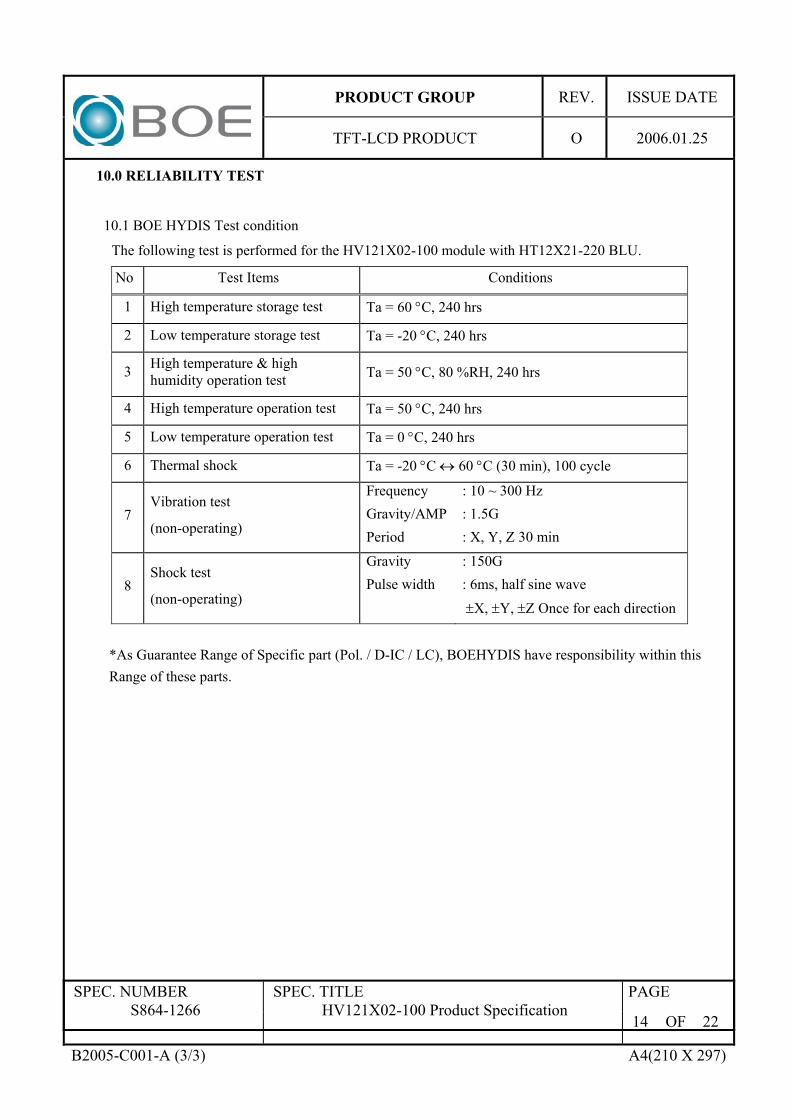
10.0 RELIABILITY TEST
10.1 BOE HYDIS Test condition
The following test is performed for the HV121X02-100 module with HT12X21-220 BLU.
No Test Items Conditions
1 High temperature storage test Ta = 60 qC, 240 hrs
2 Low temperature storage test Ta = -20 qC, 240 hrs
3 High temperature & high humidity operation test Ta = 50 qC, 80 %RH, 240 hrs
4 High temperature operation test Ta = 50 qC, 240 hrs
5 Low temperature operation test Ta = 0 qC, 240 hrs
6 Thermal shock Ta = -20 qC l 60 qC (30 min), 100 cycle
7 Vibration test
(non-operating)
Frequency
Gravity/AMP
Period
: 10 ~ 300 Hz
: 1.5G
: X, Y, Z 30 min
8 Shock test
(non-operating)
Gravity
Pulse width
: 150G
: 6ms, half sine wave
rX, rY, rZ Once for each direction
*As Guarantee Range of Specific part (Pol. / D-IC / LC), BOEHYDIS have responsibility within this
Range of these parts.

PRODUCT GROUP REV. ISSUE DATE
TFT-LCD PRODUCT O 2006.01.25
PAGE SPEC. NUMBER S864-1266
SPEC. TITLE HV121X02-100 Product Specification
15 OF 22
B2005-C001-A (3/3) A4(210 X 297)
10.2 Customer Test condition
The following test is performed with the HV121X02-100.
No Test Items Conditions Remark
1 High temperature storage test Ta = 85 qC, 50%, 240 hrs
2 Low temperature storage test Ta = -25 qC, 240 hrs
3 High temperature & high humidity operation test
Ta = 85 qC, 80 %RH, 240 hrs
4 Low temperature operation test
Ta = -25 qC, 240 hrs
5 Shock
Gravity : 120G
Pulse Width : 2ms, Half Sine
Wave for x, y, z direction
6 Vibration test
(non-operating)
Frequency : 1 ~ 300Hz
Gravity / AMP : 1.5G Period
X, y, z 30min.
PRODUCT GROUP REV. ISSUE DATE
TFT-LCD PRODUCT O 2006.01.25
PAGE SPEC. NUMBER S864-1266
SPEC. TITLE HV121X02-100 Product Specification
16 OF 22
B2005-C001-A (3/3) A4(210 X 297)
11.0 HANDLING & CAUTIONS
11.1 Cautions for handling the module
y As the electrostatic discharges may break the LCD module, handle the LCD module with care. Peel a protection sheet off from the LCD panel surface as slowly as possible.
y As the LCD panel is made from fragile glass material, impulse and pressure to the LCD module should be avoided.
y As the surface of the polarizer is very soft and easily scratched, use a soft dry cloth without chemicals for cleaning.
y Put the module display side down on a flat horizontal plane.
11.2 Other cautions
y Do not disassemble and/or re-assemble LCD module.
y When returning the module for repair or etc, please pack the module not to be broken. We recommend using the original shipping packages.

PRODUCT GROUP REV. ISSUE DATE
TFT-LCD PRODUCT O 2006.01.25
PAGE SPEC. NUMBER S864-1266
SPEC. TITLE HV121X02-100 Product Specification
17 OF 22
B2005-C001-A (3/3) A4(210 X 297)
12.0 APPENDIX
Figure 1. Measurement Set Up
OsGdG\W��PG
Figure 2. Response Time Testing
T FT O ff(B lack) T FT O n(W hite) T FT O ff(B lack)
T r
1 0 0%
9 0%
1 0%0%
T d

PRODUCT GROUP REV. ISSUE DATE
TFT-LCD PRODUCT O 2006.01.25
PAGE SPEC. NUMBER S864-1266
SPEC. TITLE HV121X02-100 Product Specification
18 OF 22
B2005-C001-A (3/3) A4(210 X 297)
Figure 3. Cross Modulation Test Description
YB - YA Cross-Talk =
YA ϧ 100
Where:
YA = Initial luminance of measured area (cd/m2)
YB = Subsequent luminance of measured area (cd/m2)
The location measured will be exactly the same in both patterns.
VIEW AREA
YA (896, 384)
256, 192
256, 576768, 576
768, 192
YB (896, 384)
VIEW AREA

PRODUCT GROUP REV. ISSUE DATE
TFT-LCD PRODUCT O 2006.01.25
PAGE SPEC. NUMBER S864-1266
SPEC. TITLE HV121X02-100 Product Specification
19 OF 22
B2005-C001-A (3/3) A4(210 X 297)
Figure 4. Packing Sequence of HV121X02-100
PANEL
PRODUCT LABEL
PACKING TRAY
SHIELDING BAGPACKING TAPE
BOX LABEL
15”BOX

PRODUCT GROUP REV. ISSUE DATE
TFT-LCD PRODUCT O 2006.01.25
PAGE SPEC. NUMBER S864-1266
SPEC. TITLE HV121X02-100 Product Specification
20 OF 22
B2005-C001-A (3/3) A4(210 X 297)
Figure 5. Product Serial Number
PRODUCT GROUP REV. ISSUE DATE
TFT-LCD PRODUCT O 2006.01.25
PAGE SPEC. NUMBER S864-1266
SPEC. TITLE HV121X02-100 Product Specification
21 OF 22
B2005-C001-A (3/3) A4(210 X 297)
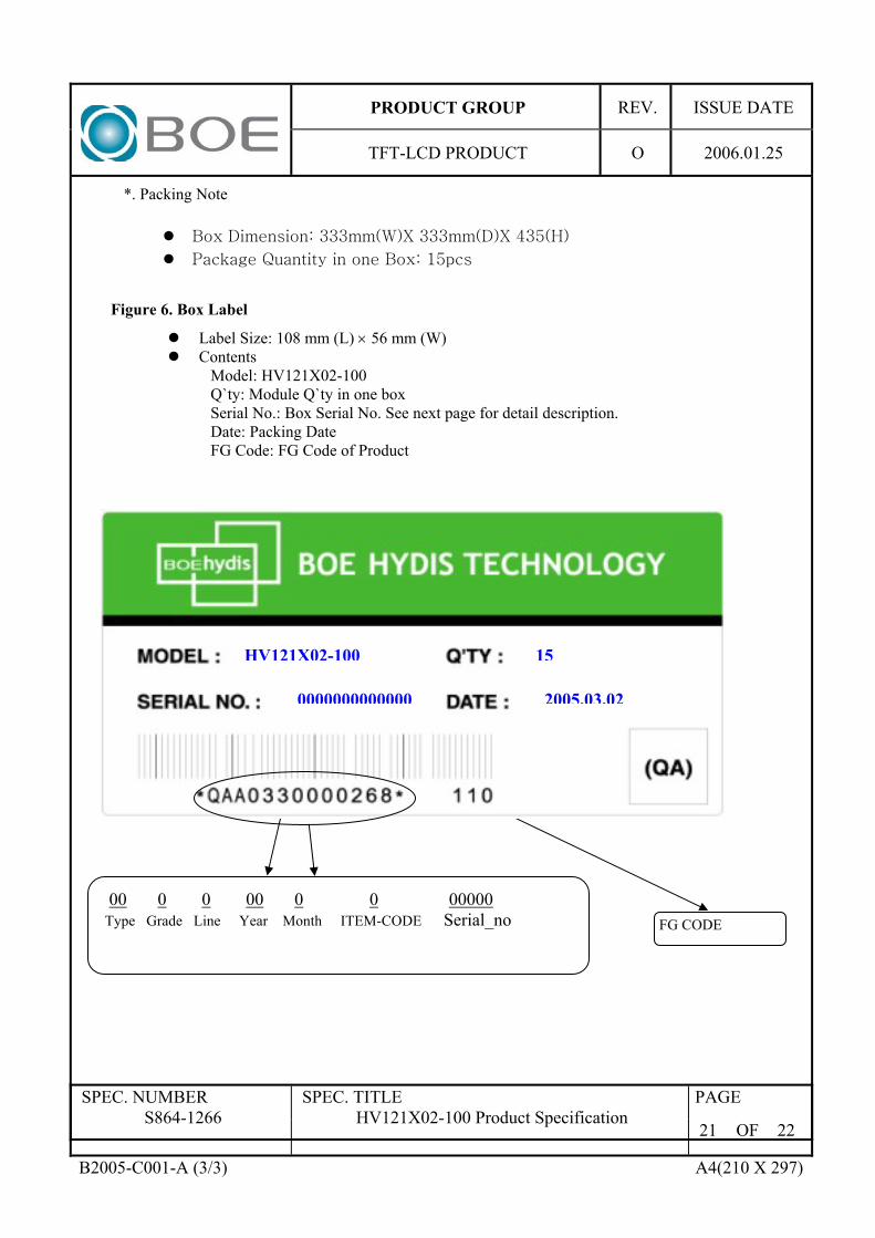
*. Packing Note
z i��Gk��������aGZZZ��O~P�GZZZ��OkP�G[Z\OoPGz w������Gx������ G��G���Gi��aGX\���
Figure 6. Box Label
z Label Size: 108 mm (L) u 56 mm (W) z Contents
Model: HV121X02-100 Q`ty: Module Q`ty in one box Serial No.: Box Serial No. See next page for detail description. Date: Packing Date FG Code: FG Code of Product
0
00 0 0 00 0 0 00000 Type Grade Line Year Month ITEM-CODE Serial_no FG CODE
HV121X02-100
0000000000000 2005.03.02
15
PRODUCT GROUP REV. ISSUE DATE
TFT-LCD PRODUCT O 2006.01.25
PAGE SPEC. NUMBER S864-1266
SPEC. TITLE HV121X02-100 Product Specification
22 OF 22
B2005-C001-A (3/3) A4(210 X 297)
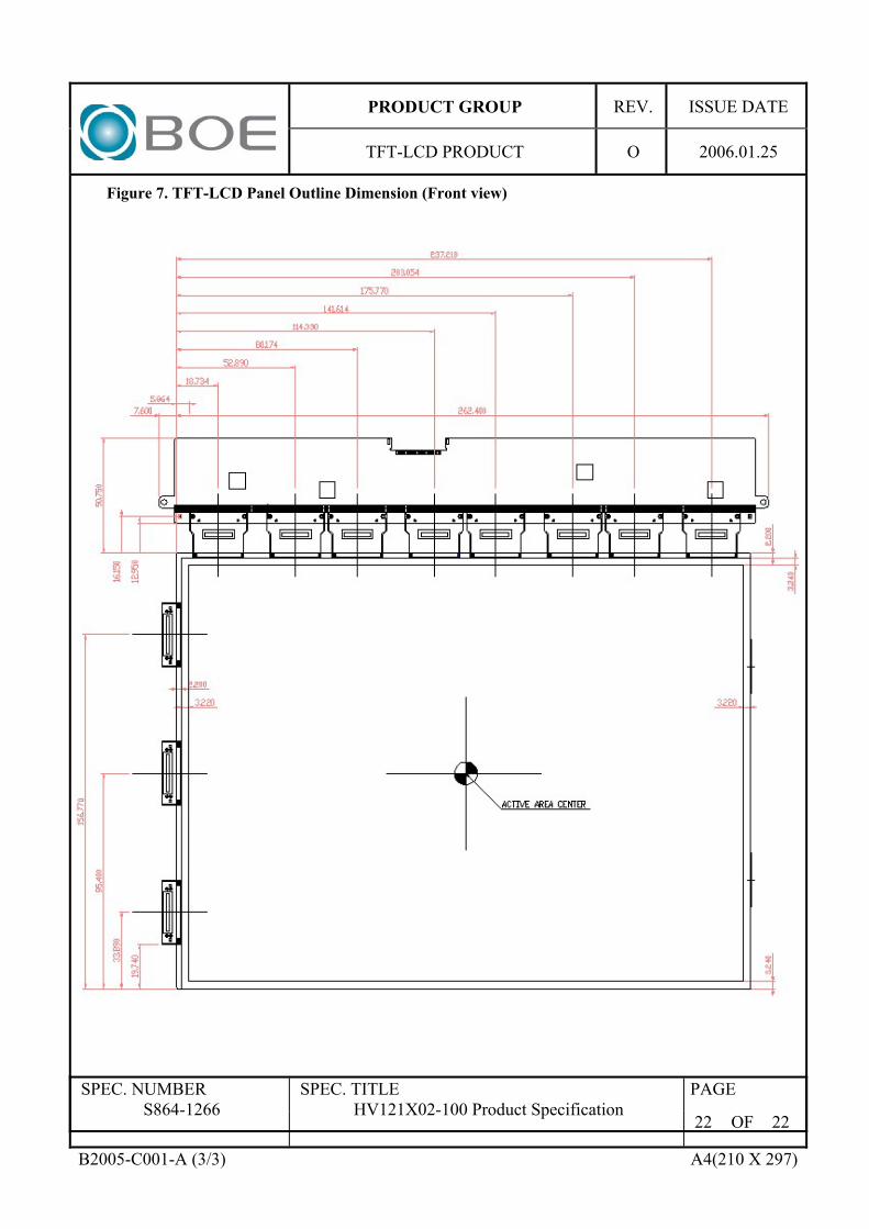
Figure 7. TFT-LCD Panel Outline Dimension (Front view)