tips and advanced techniques for characterizing a …...worked for 10 years at westel...
TRANSCRIPT

DesignCon 2014
De-Mystifying the 28 Gb/s PCB Channel:
Design to Measurement
Jack Carrel, Xilinx
Heidi Barnes, Agilent Technologies
Robert Sleigh, Agilent Technologies
Hoss Hakimi, Xilinx
Mike Resso, Agilent Technologies

i
Abstract
A design methodology will be demonstrated for 28 Gb/s SERDES channels using the Xilinx
Virtex-7 Transmitter (Tx) to show the required trade-offs that enable robust performance that is
easy to verify with measurement. Tx and Rx characterization provide information on the
spectral demands for accurate de-embedding of the passive fixture channel; simulation of cables,
connectors, vias, PCB transmission-lines, and package ball-out determine critical elements for
performance; physical routing along with test structures will determine the ability of
measurements to verify performance at the DUT package bumps. Novel 1 port fixture
measurements will be compared with previous full path probing and 2x test fixture measurement
methods to enable reliable fixture removal. Combining design and measurement methodology
enables the capture of 28 Gb/s Tx waveforms at the BGA package bumps even with frequency
dependent losses in the fixture path connection to the measuring oscilloscope.
ii
Author(s) Biography
Heidi Barnes, is a Senior Application Engineer for High Speed Digital applications in the EEsof
EDA Group of Agilent Technologies. Past experience includes over 6 years in signal integrity
for ATE test fixtures for Verigy, an Advantest Group, and 6 years in RF/Microwave microcircuit
packaging for Agilent Technologies. She rejoined Agilent Technologies in 2012, and holds a
Bachelor of Science degree in electrical engineering from the California Institute of Technology.
Mike Resso, the Signal Integrity Applications Expert in the Component Test Division of Agilent
Technologies, has over twenty years of experience in the test and measurement industry. His
background includes the design and development of electro-optic test instrumentation for
aerospace and commercial applications. His most recent activity has focused on the complete
multiport characterization of high speed digital interconnects utilizing Time Domain
Reflectometry (TDR) and Vector Network Analysis (VNA). Mike has twice received the Agilent
Technologies Spark of Insight award for his contributions to the company. Mike received a
Bachelor of Science degree in Electrical and Computer Engineering from University of
California.
Rob Sleigh is a Product Marketing Engineer for sampling scopes in Agilent Technologies’
Oscilloscope Products Division. He is responsible for product development for the division’s
high-speed electrical and optical digital communications analyzer and jitter test products. Rob’s
experience at Agilent Technologies/Hewlett-Packard includes 5 years in technical support, and
over 8 years in sales and technical marketing. Prior to working at Agilent Technologies/HP, Rob
worked for 10 years at Westel Telecommunications in Vancouver, British Columbia, Canada,
designing microwave and optical telecommunication networks. Rob earned his B.S.E.E. degree
from the University of Victoria.
Jack Carrel is an Applications Engineer at Xilinx. He has over 25 years of experience in
product development and design in the fields of Instrumentation, Test and Measurement, and
Telecommunications. His background includes development of electro-optic modules, Multi-
gigabit transceiver boards, high speed and high resolution data acquisition systems for
government and commercial applications. Most recently he has been involved in product design
using multi-gigabit transceivers with specific focus on PCB design issues. He has published in
several professional publications. Jack received his Bachelor of Science degree in Electrical
Engineering from the University of Oklahoma.
Hoss Hakimi is a Principal Engineer at Xilinx. He has 20+ years of experience at various
Telecom, semiconductor, and computer industries specializing on high level behavior modeling
and top-down design methodology in ASIC/FPGA design, synthesis, Substrate Design, 3D
Interconnect Parasitic Extraction, Understanding of high speed signal integrity and PCB power
integrity and simulation. Hoss holds an Electrical Engineering from San Jose State University,
and he has completed MS courses in the EE department at University of California Berkeley.
1
Introduction
The design of high speed digital systems requires a fundamental understanding of the
degradation encountered in the channel that lies between the transmitter and receiver. Elaborate
coding schemes, equalization, and transmission line structural designs have enabled modern
consumer electronics to easily drive past the RF domain and into the microwave frequencies of
operation. The challenges of a 28 Gb/s channel in support of 100 GB Ethernet are no different
than the original problems of the 1st trans-Atlantic copper communication cable where
transmission line theory dominates and the control of frequency dependent losses along with
reflections are the key to success.
The ability to measure the true 28 Gb/s signal parameters at the device package pins can be quite
challenging. PCB design, fixture path characterization, and instrument measurement capabilities
all contribute to the success of predicting the true signal at the package pins. By systematically
breaking down the data channel, the smaller components within can be optimized and
characterized by both measurement and simulation to achieve a controlled impedance
environment that propagates the highest of data rates Given a clear understanding of the
spectral demands placed on the transmission line by the transmitted data, it is possible to
establish a set of criteria for identifying which transmission line features require attention and
how much effort should be applied.
The design must also accommodate the ability to verify the performance through accurate
measurement techniques. Simple probing with a voltmeter is obviously not an option at 28 Gb/s.
However, well calibrated frequency domain S-parameter type measurements and advanced in-
situ de-embedding techniques have a well-established mathematical solution. These techniques
enable one to “probe” the signal path at arbitrary locations and verify the robust design of the
SERDES channel. The selection of full path probing, vs. a 2x fixture through test structure, vs. a
direct fixture measurement into a reflect open or short is not a simple cost vs. performance trade-
off. The physical design of the channel often dictates the accuracy one can achieve with the
different calibration techniques and there is opportunity to modify the design for improving the
performance of the measurements.
Often the barrier to using advanced error correction techniques such as de-embedding is the cost
in time and materials to develop the necessary calibration structures and the measurement of the
channel fixture. Work in a previously published paper[1]
showed that 2x through Automatic
Fixture Removal (AFR) calibration structures can be used to achieve a very acceptable level of
de-embedding quality. As discussed in the previous paper, keys to achieving a useful level of de-
embedding include careful design, construction, and measurement of the calibration test fixture.
It was shown that a calibration test fixture can be designed that does not require an inordinate
amount of board space and does not require the investment in micro-probing stations.
Additionally, if the high speed fixture path is properly designed to avoid large impedance
mismatches, partial S21 de-embedding provided very good results, eliminating the need to
precisely line up measurement reference planes to within picosecond precision for the cascaded
elements in the model of the fixture path. Also, it was shown that high density applications that
have 10’s of channels with significant variations in path length (electrical delay) benefitted from
a hybrid measurement based model of the channel fixture so that the effect of path length

2
variations could be simulated in a matter of seconds and reduce the board space required for 2x
through fixture calibration structures.
Implementation of these measurement calibration techniques can be done with typical stimulus-
response instrumentation such as Vector Network Analyzers or Time Domain Reflectometers.
Knowledge of the spectral demands for the channel will be used to select the required instrument
measurement bandwidth. The measurements will focus on the benefits of a 1 Port calibration
method to provide fast characterization of the channel without the need for test structures or
additional probe connections. In this new 1-Port technique, time domain gating and signal flow
diagram optimization are used to acquire the full 2-port S11, S21, S12, and S22 data set from the
measurement of the fixture channel from the S11 one-port reflection measurement. In this case,
all the S-parameters of the fixture channel are acquired and full de-embedding of the fixture can
be done during in-situ waveform measurements.
The final test of the design and measurement calibration process is to verify that one can get
back to the original performance of a transmitter (Tx) source signal even with the frequency
dependent losses of the fixture channel path in the measurement. The 2x through AFR technique
was verified in a prior publication[1]
with the Virtex-7 packaged DUT and can be used as a
reference. This same DUT will be used to evaluate the 1-Port AFR technique and further
evaluate the benefits of a measurement based model. Demonstrating that it is possible to
measure the live signal eye diagram performance at the package bumps of the Xilinx Virtex-7
transmitter opens the door for accurate transmitter models that can be used in the optimization of
application specific channel designs for 28 Gb/s.
Overview of a 28 Gb/s SERDES Channel A printed circuit board was designed and built with the following goals:
1. Provide a set of channels for carrying 28 Gb/s signals from the Xilinx FPGA to an
external device such as a piece of test equipment.
2. Provide a set of test structures that assist with de-embedding the PCB channel.
The signal path for the 28 Gb/s signals is from the Xilinx Virtex-7 FPGA to SMA connector that
is the working point for connection to devices such as test equipment (e.g. oscilloscopes) or data
transmission devices (e.g. optical transceivers), Figure 1. The components of the signal path are:
1. BGA to PCB interface structure including the solder ball pad and BGA launch structure
on the PCB.
2. Differential loosely coupled embedded stripline traces.
3. PCB to connector interface structure including vias and connector PCB pads.
4. Samtec BullsEye™ connector and test cable.
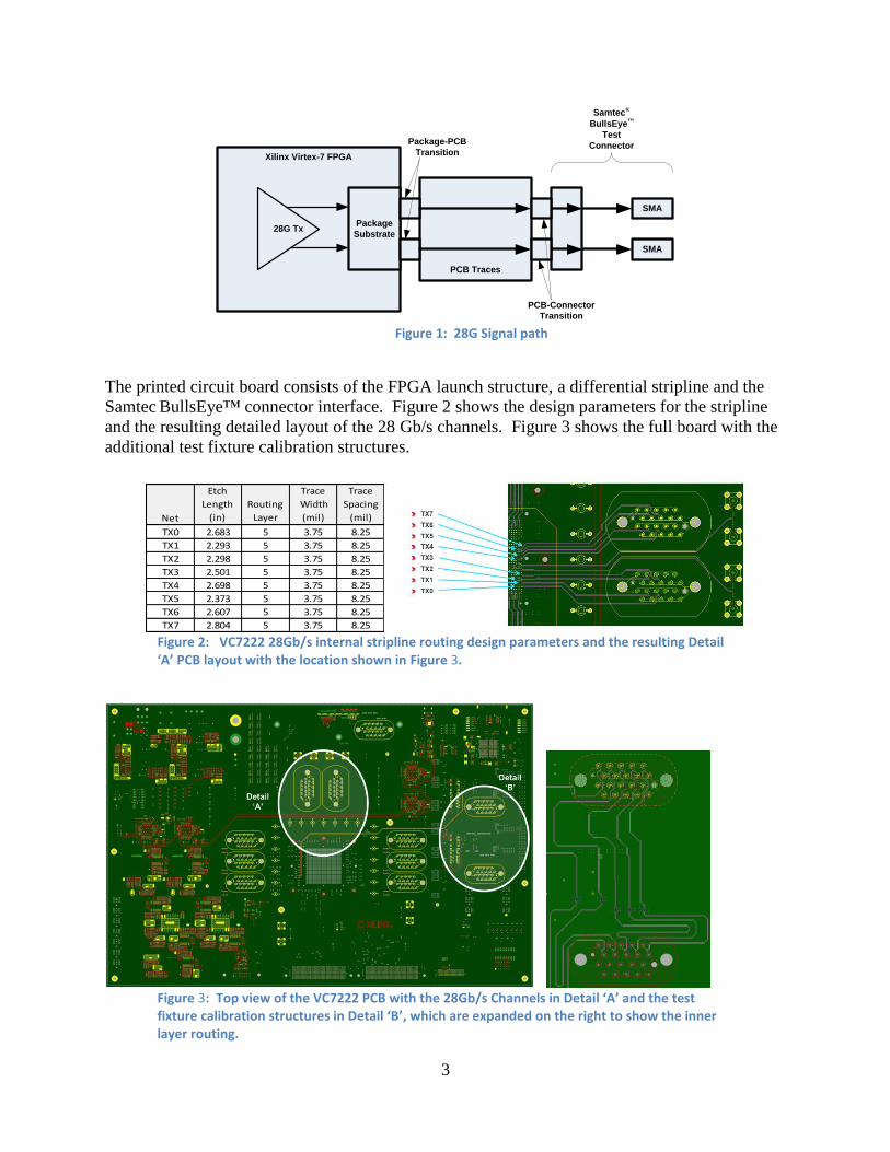
3
Xilinx Virtex-7 FPGA
28G TxPackage
Substrate
Package-PCB
Transition
PCB Traces
Samtec®
BullsEye™
Test
Connector
SMA
SMA
PCB-Connector
Transition Figure 1: 28G Signal path
The printed circuit board consists of the FPGA launch structure, a differential stripline and the
Samtec BullsEye™ connector interface. Figure 2 shows the design parameters for the stripline
and the resulting detailed layout of the 28 Gb/s channels. Figure 3 shows the full board with the
additional test fixture calibration structures.
Net
Etch
Length
(in)
Routing
Layer
Trace
Width
(mil)
Trace
Spacing
(mil)
TX0 2.683 5 3.75 8.25
TX1 2.293 5 3.75 8.25
TX2 2.298 5 3.75 8.25
TX3 2.501 5 3.75 8.25
TX4 2.698 5 3.75 8.25
TX5 2.373 5 3.75 8.25
TX6 2.607 5 3.75 8.25
TX7 2.804 5 3.75 8.25 Figure 2: VC7222 28Gb/s internal stripline routing design parameters and the resulting Detail ‘A’ PCB layout with the location shown in Figure 3.
Figure 3: Top view of the VC7222 PCB with the 28Gb/s Channels in Detail ‘A’ and the test fixture calibration structures in Detail ‘B’, which are expanded on the right to show the inner layer routing.

4
Fixture Design Analysis In the case of designing a fixture for the measurement of a transmitter at the package bumps, it is
necessary to understand the bandwidth requirements for fixture de-embedding and how this
impacts the design methodology. At 28 Gb/s the 1 bit length is only 36 ps which leaves little
room for even the fastest of step edges such as the 6.5 ps (10% to 90%) generated by Indium-
Phosphide technology for high end Test and Measurement equipment. Measurements using
fixture de-embedding techniques [1]
showed that the Virtex7 Tx rise-time at the PCB interface on
the VC7222 characterization board is ~13 ps (20% to 80%), and IC model simulations of the
transmitter without as-fabricated package/socket/pcb interface interactions estimate a best case
rise-time of 5 ps (20% to 80%)[2]
. This knowledge then enables one to speed up simulations by
not overestimating the required bandwidth, and to reduce instrument costs by understanding the
maximum required bandwidth.
At lower data rates where the rise-time was not a significant portion of the eye one would often
insist that the required bandwidth needed to include the 5th
Harmonic of the clock rate. At 28
Gb/s with a clock rate of 14 GHz this would require 70 GHz bandwidth which significantly
increases both design and measurement challenges. A more realistic rule of thumb is to look at
an exponential rise time and not an ideal step edge and see at what frequency the signal power is
reduced by 50% or 3dB. This is a reduction in voltage amplitude by 30%. A simple exponential
rising edge based on an RC time constant τ [3]
calculates this F(3dB) point for an ideal step sent
through a path with a given rise-time as:
( )
( ) ( )
( ) Equation 1
Utilizing the 20%-80% rise-time values, the faster estimate of the Tx rise-time on die of 5 ps
gives a maximum bandwidth of 44 GHz and slower rise-time measured at the package/PCB
interface of 13 ps provides a minimum bandwidth of 17 GHz. At these frequencies the design
becomes easier and there are a greater number of measurement options.
The next problem is that even though we have an estimate for the maximum bandwidth of our
time domain signal, the desire to eventually de-embed this measured S-parameter spectral
response of the path from the measurement means that it is necessary to convert the spectral
response back to the time domain. This conversion from the frequency domain back to the time
domain is based on the assumption that with a linear passive system, one can add up a series of
sinusoidal inputs to arrive at the actual time domain waveform. This is the basis of Fourier
theory as shown in Figure 4 Case 1. However, at each frequency, this assumption requires that
there are additional higher frequencies available to provide the necessary addition and
subtraction to arrive at the actual causal time domain waveform with no signal arriving before
the effective time zero arrival of the step edge. If the signal strength is significant at the
maximum frequency of the bandwidth, and additional frequencies are not available for
cancellation then one ends up with noise ripple at these higher frequencies which is also known
as the Gibb’s phenomena[4]
, Figure 4 Case 2.

5
Figure 4: A square wave can be recreated by the sum of the odd harmonic sine waves.
To see how this affects the measurement of the signal path and the desire to de-embed back to an
accurate measurement of a 13 ps rise-time signal at the Tx package, it is instructive to look at
how much measurement bandwidth will accurately re-create such a time domain signal. Starting
with a time domain pulse with a 13 ps rise-time, and 216 ps long (six “1” bits in a row at 28
Gb/s) it is easy to see the linear roll off in frequency content on the dB log plot obtained
from an FFT transform. See the plot in the lower left quadrant of Figure 5. Band-limiting this
spectral content with an abrupt brick-wall filter at 17 GHz results in ~5% ripple error on the time
domain waveform when converting back with an inverse FFT. See the plot in the upper right
quadrant of Figure 5.
Figure 5: Spectral content of a finite 13 ps edge rate pulse and then the resulting recreation of the pulse after band limiting the spectral content to 17 GHz and then doing an inverse transform back to the time domain.
Traditional windowing techniques like Bessel-Thompson with flat group delay and Hamming[5]
try to reduce the amplitude at the band limit by “throwing away” spectral amplitude at the higher
frequencies which does reduce the Gibb’s energy, but at the expense of a slower rise-time. In the
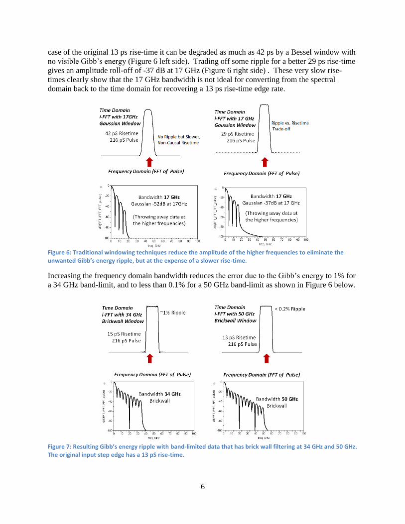
6
case of the original 13 ps rise-time it can be degraded as much as 42 ps by a Bessel window with
no visible Gibb’s energy (Figure 6 left side). Trading off some ripple for a better 29 ps rise-time
gives an amplitude roll-off of -37 dB at 17 GHz (Figure 6 right side) . These very slow rise-
times clearly show that the 17 GHz bandwidth is not ideal for converting from the spectral
domain back to the time domain for recovering a 13 ps rise-time edge rate.
Figure 6: Traditional windowing techniques reduce the amplitude of the higher frequencies to eliminate the unwanted Gibb’s energy ripple, but at the expense of a slower rise-time.
Increasing the frequency domain bandwidth reduces the error due to the Gibb’s energy to 1% for
a 34 GHz band-limit, and to less than 0.1% for a 50 GHz band-limit as shown in Figure 6 below.
Figure 7: Resulting Gibb’s energy ripple with band-limited data that has brick wall filtering at 34 GHz and 50 GHz. The original input step edge has a 13 pS rise-time.

7
Another technique that is available for dealing with the abrupt band limited data from a
measurement or an EM-simulation is to use the laws of causality to fill in the missing spectral
content that is required to cancel out the Gibb’s energy. Using a Hilbert transform that splits the
frequency-to-time domain transform into odd and even components, and then using the Kramers-
Kronig relationship that says there can’t be energy before time zero or before the time delay
required for an edge to travel through a path enables one to fill in the missing spectral content [6]
.
This missing spectral content in the frequency domain is designed to not alter the frequency
content of the time domain signal, but rather cancel out the undesired Gibb’s energy.
Comparing this with a traditional FFT exponential windowing technique with 17 GHz band-
limited data shows that the traditional method significantly corrupts the 28 Gb/s PRBS7 eye due
to the reduction in rise-time from the windowing at 17 GHz, while the causal transform method
struggles to maintain full spectral amplitude at 17 GHz, as shown in the top graphs of Figure 8.
The causal transform gets closer to the correct amplitude, but suffers from a lack of information
to truly fill in the shape of the rising edge. Increasing the bandwidth to 34 GHz provides a much
more realistic eye prediction and the causality enforced transform with 14 ps rise time is very
close to the original time domain rise-time of 13 ps.
Figure 8: Comparison of traditional windowing with the Fourier transform vs. the causality enforced Hilbert transform for channel data that is band-limited at 17 GHz and at 34 GHz for a 28 Gb/s PRBS7 transmission.
Going out to 50 GHz results in the correct rise time for the causality enforced transform, and
then at 150 GHz both methods easily achieve an accurate recreation of the time domain signal.

8
Figure 9: Comparison of traditional windowing with the Fourier transform vs. the causality enforced Hilbert transform for channel data that is band-limited to 50 GHz and 150 GHz for a 28 Gb/s PRBS7 transmission.
This analysis provides the information needed to understand the required bandwidth of the
measured or simulated S-parameter behavioral model of the fixture channel such that when it is
de-embedded from the in-situ measurement of the SERDES transmitter one can have the
necessary bandwidth to accurately characterize the Tx signal at the BGA package bumps.
Fixture Removal Methodology
Precision probing on high-speed devices requires high-bandwidth probes and a probe station
with a camera[7]
. However, for optimum measurement fidelity and ease-of-use, accurate device
characterization is usually performed by connecting test equipment to the device-under- test
(DUT) via a fixture and high quality coaxial cables.
If the high speed channel fixture degrades the signal from the DUT, the resultant signal measured
by the test equipment will be distorted. However, if the fixture is accurately characterized
through measurement or modeling (or ideally both), it is possible to remove, or de-embed, the
effects of the frequency dependent losses of the fixture and/or cables from the measurement. It
is important to note that de-embedding should not be expected to absolve the designer from
using good fixture design techniques and materials. De-embedding has its limitations and every
effort should be used to minimize signal degradation due to a fixture.
Many different approaches have been developed for removing the effects of the test fixture from
the physical layer measurement and these approaches fall into two fundamental categories: direct
measurement (pre-measurement process) and de-embedding (post-measurement processing). An
approximation of ease of use and accuracy of these two techniques is shown in Figure 10. Direct
measurement requires specialized calibration standards that are inserted into the test fixture and
measured. The accuracy of the device measurement relies on the quality of these physical
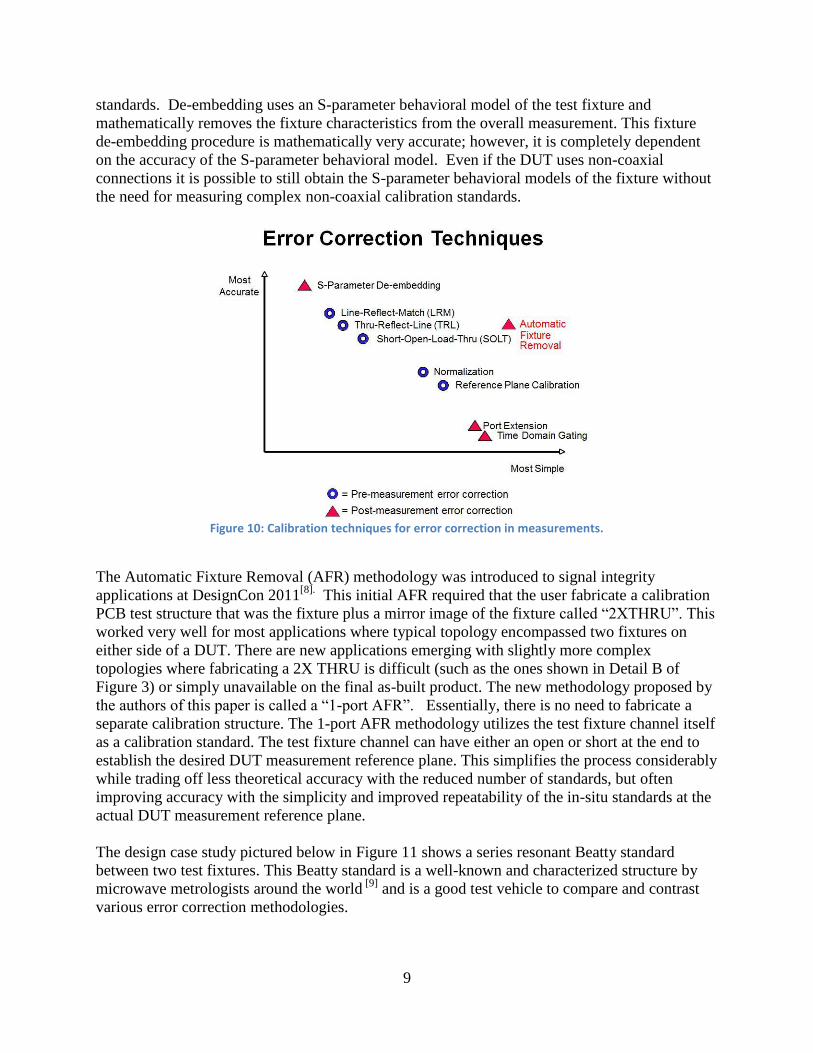
9
standards. De-embedding uses an S-parameter behavioral model of the test fixture and
mathematically removes the fixture characteristics from the overall measurement. This fixture
de-embedding procedure is mathematically very accurate; however, it is completely dependent
on the accuracy of the S-parameter behavioral model. Even if the DUT uses non-coaxial
connections it is possible to still obtain the S-parameter behavioral models of the fixture without
the need for measuring complex non-coaxial calibration standards.
Figure 10: Calibration techniques for error correction in measurements.
The Automatic Fixture Removal (AFR) methodology was introduced to signal integrity
applications at DesignCon 2011[8].
This initial AFR required that the user fabricate a calibration
PCB test structure that was the fixture plus a mirror image of the fixture called “2XTHRU”. This
worked very well for most applications where typical topology encompassed two fixtures on
either side of a DUT. There are new applications emerging with slightly more complex
topologies where fabricating a 2X THRU is difficult (such as the ones shown in Detail B of
Figure 3) or simply unavailable on the final as-built product. The new methodology proposed by
the authors of this paper is called a “1-port AFR”. Essentially, there is no need to fabricate a
separate calibration structure. The 1-port AFR methodology utilizes the test fixture channel itself
as a calibration standard. The test fixture channel can have either an open or short at the end to
establish the desired DUT measurement reference plane. This simplifies the process considerably
while trading off less theoretical accuracy with the reduced number of standards, but often
improving accuracy with the simplicity and improved repeatability of the in-situ standards at the
actual DUT measurement reference plane.
The design case study pictured below in Figure 11 shows a series resonant Beatty standard
between two test fixtures. This Beatty standard is a well-known and characterized structure by
microwave metrologists around the world [9]
and is a good test vehicle to compare and contrast
various error correction methodologies.

10
Figure 11: The simple series resonant Beatty standard is used to verify the AFR calibration methodology.
The impedance profile of the Beatty standard is shown below in Figure 12 for the following
methods: TRL Calibration (Thru-Reflect-Line), Generation 1 Automatic Fixture Removal (AFR)
using 2XTHRU and finally the proposed Generation 2 AFR using 1-port. As one can easily see,
all methods correlate quite well with each other.
Figure 12: Comparison of the quality of the fixture de-embed vs. the type of calibration used for obtaining the full S-parameter behavioral model of the fixture channel.
The benefit of fixture de-embedding is clearly seen when looking at the insertion loss and return
loss data. Before removing the fixture, there are multiple resonant structures in the physical layer
channel with the Beatty structure. This can be seen by looking at the very choppy red S21 and
blue S11 waveforms depicted in the lower left portion of Figure 13. However, after the automatic
fixture removal is performed (after de-embed), the harmonics of the ¼ wavelength resonances
from the single series impedance discontinuity are clearly visible in the very periodic and smooth
data in the lower right portion Figure 13.

11
Figure 13: Benefits of fixture de-embedding verified using a simple series resonant Beatty structure.
It is worth noting that the “ripple” or structure in the frequency domain due to reflections
between the fixture and the device under test require full S-matrix de-embedding. Just de-
embedding the S21 adjusts the overall magnitude but does not change the ripple due to
reflections. This is clearly seen in the analysis of the Beatty example where the DUT has a 1x
fixture on either side creating multiple reflections that require a full S-matrix de-embed.
However, in the case of de-embedding for an in-situ Tx measurement, there is only a single 1x
fixture terminated at the Tx. In the case where the Tx is impedance matched and can absorb any
reflections coming from the channel fixture, then only the S21 data is needed for de-embedding
the frequency dependent losses of the fixture channel. This partial de-embedding still captures
the frequency dependent losses of the multiple impedance discontinuities within the channel, but
is less sensitive to electrical length differences between the S-parameter behavioral model of the
fixture channel and the in-situ fixture channel during measurement.
It is worth noting that electrical length differences as small as 12 mils (the thickness of a sheet of
paper) caused by cable movement, variations in adapters, connector mating repeatability, etc. can
cause significant errors at higher frequencies when trying to implement full de-embedding of the
S-parameter matrix. Partial de-embedding of the transmitted insertion loss (S21) of the channel
with a Tx impedance matched to absorb reflections from the fixture channel can be a better
option than full S-matrix de-embedding as shown in the right side of Figure 14. If the Tx is
perfectly impedance matched then the center black trace shows that there is 0 dB of error with
the partial de-embed. If the Tx is not a perfect match then the blue solid trace in the graph shows
the dB of error for the channel loss with .1nF of mismatch at the Tx. Comparing this with the
red dashed trace of a full S-matrix de-embed when there is only 12 mils of electrical length
difference between the in-situ channel length and that of the S-parameter behavioral model
shows that the full de-embed has larger errors then the partial de-embed.

12
Figure 14: Full S-matrix de-embedding vs. partial S21 de-embedding.
The Gen 2 1-Port AFR utilizes a suite of proprietary microwave algorithms to obtain enough
information about the fixture S-parameters to perform the full s-matrix de-embedding. This
means that from a 1-Port measurement (*.s1p in Touchstone format) into an open or short it is
possible to use both time and frequency domain information to fully populate the 2 x 2 S-
parameter matrix (*.s2p ). This is a complete behavioral model of the single-ended fixture that
includes forward return loss, forward insertion loss, reverse return loss, and reverse insertion
loss. Since most high speed digital channels are differential, the Gen 2 AFR can also perform
the same transformation with a differential fixture. In this case the input port to the differential
pair is connected to the measurement system, and the output at the desired DUT measurement
reference plane is terminated in an open or short. This differential pair measurement from one
side (*.s2p) with the other end left open or shorted can then be used for calculating the full 4-port
S-parameter behavioral model (*.s4p). This is a complete behavioral model of the differential
fixture that has all 16 parameters including mixed mode S-parameters. This is depicted
graphically by Figure 15.
Figure 15: Gen 2 1-Port AFR utilizes a simple 1 port measurement of the in-situ fixture path terminated in a reflect (open and/or short) at the DUT measurement reference plane to populate the full 16 parameter S-matrix behavioral for the 4-port 1x fixture channel.
This new Gen-2 1-Port AFR method for measuring the 28 Gb/s channel fixture can now be
compared with the prior art Gen-1 2XTHRU method and the flexible measurement based ADS
model. A quick look at the insertion loss in Figure 16 shows that the 2XTHRU path with the
double fixture length and difficulties in symmetry at the BGA reference via location are not ideal
for maintaining the calibration quality past 37 GHz. The new 1-Port AFR does not suffer from
the symmetry issues and the calibration is continuous to 50 GHz with no jumps in data.

13
Figure 16: Frequency domain insertion loss and time domain TDR of the 3 different fixture behavioral models.
The ADS model avoids the calibration anomalies, but is conservative in the loss estimates at
higher frequencies so that one does not over compensate with the de-embed of the channel losses
and make the Tx signal look better than it is. The time domain plot is a quick reference to show
that all 3 fixtures line up with the same locations of the channel discontinuities and the relative
magnitudes. The ADS model does capture the major impedance discontinuities of the channel,
but not the small variations of the 3-dimensional material properties and fabrication processes.
28 Gb/s SERDES Measurements As high-speed electrical communication systems and components increase in data rates to 28
Gb/s and beyond, design and validation engineers are faced with the difficult task of accurately
characterizing the true performance of their designs.
To accurately characterize a high-speed device such as 28 Gb/s SERDES, it is important to
perform measurements using a receiver with the following attributes:
1. Sufficient Bandwidth
2. Compliant Clock Recovery
3. Low random noise/jitter
Receiver Bandwidth
For accurate analysis the receiver measuring the signal must have sufficient bandwidth to capture
all the energy of the signal. Using a receiver with sufficient bandwidth will ensure edge speeds
are accurately represented, for example, performing an FFT on the TX signal from the Xilinx
Virtex-7 we determined that there was little spectral content above 50 GHz (See purple trace in
Figure 17, below). Since sampling scopes typically have negligible random noise compared to
the device under test, we chose to use a receiver with 50 GHz bandwidth.
14
Figure 17: FFT of transmitter signal indicates spectral content to 50 GHz. The purple includes the 1x fixture in the path, and the orange is with the 1x fixture de-embedded from the measurement.
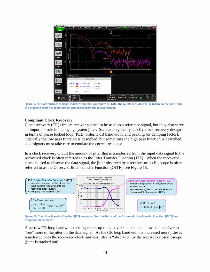
Compliant Clock Recovery
Clock recovery (CR) circuits recover a clock to be used as a reference signal, but they also serve
an important role in managing system jitter. Standards typically specify clock recovery designs
in terms of phase locked loop (PLL) order, 3 dB bandwidth, and peaking (or damping factor).
Typically the low pass function is described, but sometimes the high pass function is described,
so designers must take care to emulate the correct response.
In a clock recovery circuit the amount of jitter that is transferred from the input data signal to the
recovered clock is often referred to as the Jitter Transfer Function (JTF). When the recovered
clock is used to observe the data signal, the jitter observed by a receiver or oscilloscope is often
referred to as the Observed Jitter Transfer Function (OJTF), see Figure 18.
Figure 18: The Jitter Transfer Function (JTF) low-pass filter function and the Observed Jitter Transfer Function (OJTF) are frequency dependent.
A narrow CR loop bandwidth setting cleans up the recovered clock and allows the receiver to
“see” more of the jitter on the data signal. As the CR loop bandwidth is increased more jitter is
transferred onto the recovered clock and less jitter is “observed” by the receiver or oscilloscope
(jitter is tracked out).

15
Figure 19: Block diagram of a clock recovery circuit with narrow and wide loop bandwidth settings.
Many industry Standards and Implementation Agreements (IA) require that jitter measurements
must be performed using a 1st Order PLL clock recovery model, despite the fact that real clock
recovery circuits implemented in hardware usually have much higher order PLLs [10]
. Real-time
oscilloscopes usually employ software CR techniques which generate an “ideal” CR response.
Due to their architecture, sampling scopes and BERTs employ hardware clock recovery designs.
However, while instrumentation-grade hardware clock recovery circuits often have settings to
emulate a 1st Order PLL, they typically do not have “ideal” performance and therefore include
some peaking in the response. This peaking will increase jitter results and degrade measurement
accuracy. To mitigate this issue, some scopes, such as the 86108B with Option JSA, combine
hardware clock recovery (required by sampling scopes and BERTs) with an “ideal” SW PLL
model. For more details on clock recovery and how to apply an “ideal” SW clock recovery
model to a hardware clock recovery response refer to the online 86108B Clock Recovery
Overview video [11]
.
Intrinsic Oscilloscope Random Jitter Considerations
As bit rates increase the bit period decreases making jitter margins much tighter. Jitter
measurements reported by test equipment include random jitter generated by the device itself,
but they also include random jitter generated by the equipment’s internal time base (not to
mention induced jitter due to AM-to-PM conversion due to random noise/slew rate).
For optimal measurement analysis it is important to select a scope that has both low intrinsic
jitter and noise. Often users would like the test equipment to not affect the measurement by
more than 10% which means the equipment intrinsic jitter will need to be much smaller than that
of the device under test. As an example, for transmitters with expected random jitter < 220 fs
rms, it is recommended to use a scope having intrinsic random jitter < 100 fs and low random
noise (< 1mV rms).
Test Equipment Selection
For this reason, we chose to conduct this experiment using the 86100D DCA-X sampling
oscilloscope with 86108B precision waveform analysis module. The 86108B 35/50 GHz
bandwidth module has an integrated 32 Gb/s “Golden PLL” clock recovery (CR) circuit and an
internal time-base with random jitter < 50 fs rms typical. This combination of wide-bandwidth,
low noise, and low intrinsic jitter ensures that signal degradation due to the scope is negligible.

16
As mentioned above, 86108B combines an instrument-grade clock recovery design with the
ability to model “ideal” software clock recovery design. This additional clock recovery
emulation (CRE) capability yields greater jitter measurement accuracy compared to other
hardware based clock recovery designs.
Transmitter device measurements – de-embed the fixture using S-parameter models.
We validate the 1-port AFR de-embedding method by performing waveform, eye diagram, and
jitter measurements on an actual device, and correlate the results to measurements obtained using
S-parameter files that were generated using 2x Thru AFR measurements and ADS simulation
(validated in a previous paper[1]
).
Using the Agilent 86100D DCA-X wide-bandwidth oscilloscope the output of the Xilinx Virtex-
7 transmitter (TX) was measured at the coaxial connectors of the fixture.
Figure 20: Test setup showing the Xilinx Virtex-7 FPGA connected to the 86100D DCA-X via the Xilinx test fixture and Samtec® BullsEye™ cable.
TX measurements were performed on the following signals:
1. Fixture Output (no de-embed)
2. TX Output after fixture de-embed using Gen 1 1-Port AFR
3. TX Output after fixture de-embed using Gen 2 2XTHRU AFR
4. TX Output after fixture de-embed ADS Model
Graphically, this is the setup used to perform the measurement and subsequent de-embedding.

17
Figure 21: Transmitter fixture channel path with the different options for removing the lossy fixture from the measurement.
Instrument Setup
The 86100D DCA-X was setup as follows:
Oscilloscope Bandwidth – 50 GHz
Clock Recovery
Data Rate: 28.05 Gb/s
Loop Order: 1st Order
PLL Bandwidth: Data Rate/1667 (16.8 MHz)
Peaking: 0dB (due to 1st Order selection)
De-embedding was accomplished using 86100D-SIM InfiniiSim-DCA software. This software
runs on the 86100D mainframe (or offline on a PC) and allows users to de-embed a signal in
real-time, or run an off-line analysis on saved waveforms.
Figure 22: Graphical representation of the signal processing setup used to compare the de-embedded signals (the same input signal is processed by three different S-parameter models)
18
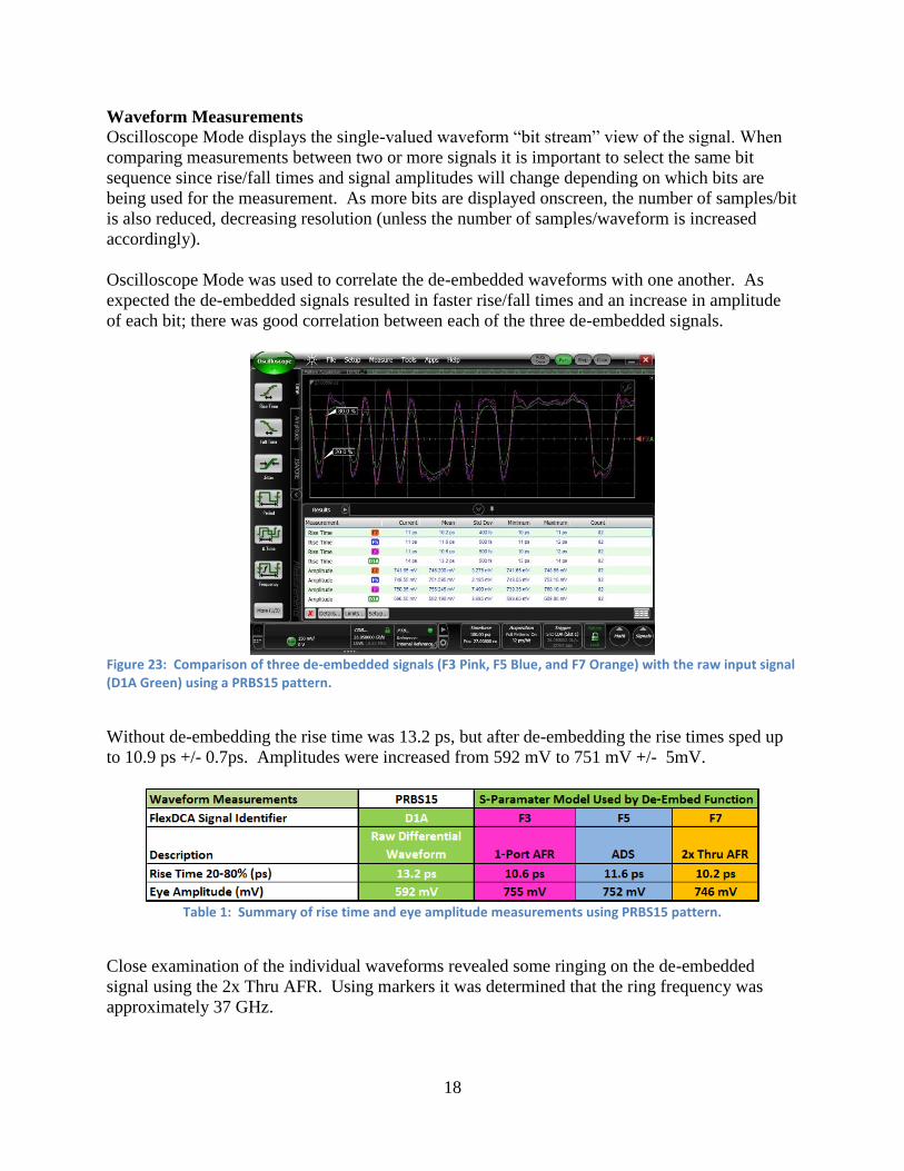
Waveform Measurements
Oscilloscope Mode displays the single-valued waveform “bit stream” view of the signal. When
comparing measurements between two or more signals it is important to select the same bit
sequence since rise/fall times and signal amplitudes will change depending on which bits are
being used for the measurement. As more bits are displayed onscreen, the number of samples/bit
is also reduced, decreasing resolution (unless the number of samples/waveform is increased
accordingly).
Oscilloscope Mode was used to correlate the de-embedded waveforms with one another. As
expected the de-embedded signals resulted in faster rise/fall times and an increase in amplitude
of each bit; there was good correlation between each of the three de-embedded signals.
Figure 23: Comparison of three de-embedded signals (F3 Pink, F5 Blue, and F7 Orange) with the raw input signal (D1A Green) using a PRBS15 pattern.
Without de-embedding the rise time was 13.2 ps, but after de-embedding the rise times sped up
to 10.9 ps +/- 0.7ps. Amplitudes were increased from 592 mV to 751 mV +/- 5mV.
Table 1: Summary of rise time and eye amplitude measurements using PRBS15 pattern.
Close examination of the individual waveforms revealed some ringing on the de-embedded
signal using the 2x Thru AFR. Using markers it was determined that the ring frequency was
approximately 37 GHz.

19
Figure 24: Ringing on a de-embedded signal (F7 Orange in this case) is often caused by S-parameters with excessive loss, or insufficient bandwidth.
This ringing is caused by a null at 37 GHz in the 2xThru S-parameter model. This can be
attributed to the calibration error caused by the challenges of trying to maintain symmetry with
the 2xThru structure. Limited space for routing and mirror imaging of the BGA via topology are
not ideal for maintaining this required symmetry at higher frequencies. The de-embedding
software must roll-off the de-embed function at the point where high attenuation requires
excessive gain, and this can introduce ringing in the response due to the aforementioned Gibbs
phenomenon. To avoid this issue, one may need to improve the quality of the 2xThru test
structure (and re-measure) or post process the data to remove the calibration anomalies. If these
options are not available, then one can roll off the de-embed function at a spectral null in the
signal (for example, on a 28 Gb/s data signal, spectral nulls occur at 28 GHz and 56 GHz) to
minimize ringing due to band-limiting.
In addition to comparing results over a specific bit sequence, we can also examine the impact
from all bits in the pattern using an Eye Diagram.
Eye Diagram Measurements
Eye diagrams wrap all bit sequences from a signal into a single unit interval. This view of a
signal makes it very fast and efficient to evaluate a transmitter’s overall performance. Since all
transitions are included the measurement, results are not specific to particular edge or bit
sequence (which can be obtained by looking at the single-valued waveform in Oscilloscope
Mode).

20
Figure 25: Eye diagram showing the output of the fixture (D1A Green) and the de-embedded signals.
Separating the de-embedded signals (see Figure 26) allows us to see that there is good
correlation between the eye diagrams. These signals represent what the signal looks like at the
balls of the device. TX emphasis can be seen on the signal(s) which helps to overcome the high-
frequency loss in the channel.
Figure 26: Comparison of de-embedded signals using S-parameter models generated using three different methods (Top: 1-port AFR; Middle: ADS; Bottom: 2x-Thru AFR).
As shown in Table 2, the PRBS15 rise time measurements improved by 3.4 ps (22%) after the
signal was de-embedded, and eye amplitude increased by over 150 mV (25%). Rise Time and
Eye Amplitude results correlated very well between de-embedding models also. Eye Height and
Jitter (rms) also show significant improvement when the raw signal was de-embedded (over 20%
and 45% respectively), but correlation between de-embedding models was not quite as good.

21
Eye Height measurements using the 1-Port AFR model (F3) showed more eye closure than the
other two methods (455 mV vs. ~540 mV). The 2x Thru AFR model (F7) resulted in a slightly
higher jitter result than the other de-embed models (702 fs vs. ~ 600 fs).
Table 2: Summary of Eye Diagram results using PRBS7 and PRBS15 patterns.
A more comprehensive analysis of the de-embedded waveforms can be realized by
separating jitter and amplitude impairments into constituent components and looking at inter-
symbol interference (ISI).
Jitter and Amplitude Analysis
De-embedding allows us to see the true performance of the DUT at the balls of the device by
removing deterministic jitter (DJ) caused by the fixture. To quantify this improvement in
jitter performance, an in-depth jitter and amplitude analysis was performed using Agilent
86100D-200/300 Enhanced Jitter and Amplitude Analysis software. This software measures
random jitter and noise using both spectral and tail fit algorithms, and reports the result
which has the lowest uncertainty [12]
.
As expected, random jitter (RJ) did not change significantly when the raw signal was de-
embedded. De-embedding only compensates for deterministic effects, but RJ results can
change slightly due to changes in the signal’s slew rate (AM-to-PM conversion converts
random noise (RN) into random jitter as a function of slew rate) [10]
. Since RN on the signal
and oscilloscope was low, RJ did not change significantly (< 10 fs rms).
ISI did improve as a result of de-embedding the test fixture, and as a result, DJ and TJ were
also reduced (ISI is a sub-component of DJ, and TJ is comprised of both RJ and DJ). Using a
PRBS7 the 1-port AFR model and the 2x Thru AFR model reduced the ISI by ~ 1.3 ps, or
35%. The ADS S-parameter model reduced ISI by 1.9 ps, or over 50%. Total jitter (TJ) on
this 28 Gb/s signal was reduced by over 1.7 ps to ~ 6 ps.

22
Table 3: Detailed jitter analysis shows the reduction in jitter when the test fixture was de-embedded using three different models.
Table 4: Inter-symbol interference (ISI) improvements using a PRBS15 test pattern.
Figure 27: Jitter analysis results on raw signal (left) and de-embedded signal using 1-port AFR model (right).
Measurement Summary: Using Agilent’s 1-Port AFR model to de-embed fixture effects from a
Xilinx Virtex-7 transmitting a 28.05 Gb/s PRBS15 provided the following improvements in
signal quality:
Rise Time: 3.4 ps faster (22% improvement)
Eye Amplitude: 150 mV higher (25% improvement)
Inter-symbol Interference (ISI): 1.7 ps lower (26% improvement)
Conclusion
The desire to easily measure a state-of-the-art 28 Gb/s transmitter at the output of a high density
FPGA package creates some interesting challenges. The design of the fixture channel must
provide a high density reasonably priced connection to the transmitter. The path from the

23
transmitter travels through a planar PCB stripline on an inner layer and then transitions through a
high density SMT connector to a coaxial cable for connection to the measuring instruments.
The frequency dependent losses of this fixture channel can theoretically be de-embedded from
the measurement assuming one can fully characterize the fixture channel path with an S-
parameter behavioral model. In reality, one must do some up front planning to get the desired
level of accuracy for the S-parameter behavioral model. Bandwidth analysis shows the problems
of band-limited measured data that have long plagued their re-use in the simulation world are
now also an issue when trying to implement de-embedding in the measurement world on a live
signal. Insufficient bandwidth can result in the Gibb’s phenomena causing non-causal effects
and added ringing in the data. At 28 Gb/s data rates with ~13 ps rise-time edges the 50 GHz
characterization of the channel is still sufficient, however, at these high frequencies other
challenges can arise.
The full S-parameter matrix de-embed with reflection and transmission terms is desired for
removing the fixture channel, but often this requires significant additional effort in order to avoid
any electrical length differences due to cable movement, variations in adapters, connector mating
repeatability, etc. In the case of the ADS model, and the Gen 1 2XTHRU they both would
require slight corrections of the electrical length to match exactly with the final in-situ
measurement. Even a small 12 mil variation in electrical length (the thickness of a sheet of
paper) can cause significant errors in the spectral content above 25 GHz for the full S-matrix de-
embed process. The Gen 2 1-Port AFR still requires connections to be mated and de-mated for
going to different measurement equipment, but the use of the exact measurement path for
extraction of the behavioral model can help to mitigate some of these path length differences,
and simplify the calibration process. Another option is to have a well-designed termination at
the source, as in the case of the Virtex 7 28 Gb/s transmitter, such that reflections from the
fixture channel back into the transmitter are absorbed. With reflections minimized from the
transmitter, then one can implement partial S21 de-embedding which is insensitive to small
electrical length differences between the S-parameter fixture channel behavioral model and the
fixture channel during the in-situ measurement.
In conclusion, utilizing the right combination of measurement and simulation techniques
explored in this paper, it has been shown that the previously existing barriers for using de-
embedding have been eliminated. Ultimately, this enables a breakthrough toolset that high speed
design engineers can confidently use for evaluating the quality of their next generation of
product designs.

24
References
1. J. Carrel, R. Sleigh, H. Barnes, H. Hakimi, and M. Resso, “Tips and Advanced
Techniques for Characterizing a 28 Gb/s Transceiver”, DesignCon 2013 (13-TP5)
2. Link to Xilinx 28Gb/s Serial Transceiver Technology
3. Stephen H. Hall, G. Hall, and J. McCall, A Handbook of Interconnect theory and Design
Practices; John Wiley & Sons, Inc., 2000(ISBN 0-471-36090-2).
4. Eric Bogatin, Signal Integrity - Simplified, Chapter 7; Prentice Hall, 2003 (ISBN 0-13-
066946-6).
5. Bracewell, R., The Fourier Transform and Its Applications. New York: McGraw-Hill,
1965.
6. Colin Warwick, “Understanding the Kramers-Kronig Relation Using A Pictorial Proof”
Agilent Technologies, Inc. 2010, White Paper 5990-5266EN.
7. R. Schaefer, Comparison of Fixture Removal Techniques for Connector and Cable
Measurements, Signal Integrity Workshop, IMS 2010.
8. E. Bogatin and M. Resso, “A Simple, Yet Powerful Method to Characterize Differential
Interconnects”, DesignCon 2011 Education Forum.
9. Beatty, R. N. “2-Port λG/4 Waveguide Standard of Voltage Standing-Wave Ratio”,
Electronics Letters, 25th
January 1973, Vol.9 No. 2.
10. Dennis Derickson, Markus Müller, Digital Communications Test and Measurement,
Chapter 9; Prentice Hall, 2008 (ISBN 0-13-220910-1).
11. Link to the 86108B Clock Recovery Overview and Demo
http://www.youtube.com/watch?v=CwmogDzPuH8
12. 86100D-200 Enhanced Jitter Analysis Software built-in documentation.
www.agilent.com/find/86100D-200