ths4509 広帯域、低ノイズ、低歪み率、完全差動アンプ (rev. i)
TRANSCRIPT

250 W
0.1 Fm
250 W
+V = 5 VS 10 nF
10 nF
Mini-Circuits
ADT2-1T
1:1.4
953 W
VIN
VCM
50 W
50 W
Mini-Circuits
ADT2-1T
1:1.4
= 20 dB
VOUT
+
-
THS4509
VIN
VOUT
Copyright © 2016, Texas Instruments Incorporated
-120
-110
-100
-90
-80
-70
-60
0 50 100 150 200 250
f - Frequency - MHz
Product
Folder
Sample &Buy
Technical
Documents
Tools &
Software
Support &Community
英語版のTI製品についての情報を翻訳したこの資料は、製品の概要を確認する目的で便宜的に提供しているものです。該当する正式な英語版の最新情報は、www.ti.comで閲覧でき、その内容が常に優先されます。TIでは翻訳の正確性および妥当性につきましては一切保証いたしません。実際の設計などの前には、必ず最新版の英語版をご参照くださいますようお願いいたします。
English Data Sheet: SLOS454
THS4509JAJS106I –JANUARY 2005–REVISED JULY 2016
参参考考資資料料
THS4509 広広帯帯域域、、低低ノノイイズズ、、低低歪歪みみ率率、、完完全全差差動動アアンンププ
1
1 特特長長1• 完全差動アーキテクチャ• 電源電圧の中点の同相入力範囲• 出力同相モード制御• 2V/V (6dB)の最小ゲイン• 帯域幅: 1900MHz• スルーレート: 6600V/μs• 1%セトリング・タイム: 2ns• HD2: 100MHzで–75dBc• HD3: 100MHzで–80dBc• OIP3: 70MHzで37dBm• 入力電圧ノイズ: 1.9 nV/√Hz (f > 10MHz)• 電源電圧: 3V~5V• 電源電流: 37.7mA• パワーダウン時電流: 0.65mA
2 アアププリリケケーーシショョンン• 5Vデータ収集システム
高直線性ADCアンプ• ワイヤレス通信• 医療用画像処理• 試験/測定機器
3 概概要要THS4509は広帯域の完全差動オペアンプで、5Vのデー
タ収集システム用に設計されています。1.9nV/√Hzの低ノ
イズで、高調波歪みも100MHz、2VPP、G = 10dB、1kΩ負荷で–75dBc HD2および–80dBc HD3と低いのが特長
です。スルーレートが6600V/μsと高く、セトリング・タイムは
1% (2Vステップ)に対して2nsであるため、パルスを使用
するアプリケーションに理想的です。最小ゲインは6dBに設計されていますが、10dBのゲインに最適化されてい
ます。
A/Dコンバータ(ADC)へのDCカップリングを可能にするた
め、独自の出力同相制御回路により、設定電圧から3mVオフセット(標準値)内に出力同相電圧が維持されます。こ
のときの条件は、設定電圧が電源電圧の中点から0.5Vの範囲内であり、差動オフセット電圧が4mV未満です。同
相電圧の設定点は内部回路により電源電圧の中点に設
定され、また外部電源からオーバードライブすることができ
ます。
入力および出力は、同相電圧を電源電圧の中点に設定し
たときに最高の特性になるように最適化されています。低
電源電圧時の高性能と合わせて、この設計は高性能の単
一電源5Vデータ収集システムに理想的です。THS4509の総合的な性能は、ADS5500 ADCを駆動し、10dBゲイ
ン、125MSPSのサンプリング速度のとき、SFDRが81dBc、SNRが69.1dBc、70MHzにおいて-1dBFS信号です。
THS4509はクワッドのリードレスVQFN-16パッケージ
(RGT)で供給され、完全な工業用温度範囲の-40~-85で動作が規定されています。
製製品品情情報報(1)
型型番番 パパッッケケーージジ 本本体体ササイイズズ(公公称称)THS4509 VQFN (16) 3.00mm×3.00mm
(1) 提供されているすべてのパッケージについては、データシートの末尾にある注文情報を参照してください。
テテスストト構構成成 測測定定さされれたた3次次のの相相互互変変調調ススププリリアアスス信信号号レレベベルル
2
THS4509JAJS106I –JANUARY 2005–REVISED JULY 2016 www.ti.com
Copyright © 2005–2016, Texas Instruments Incorporated
目目次次1 特特長長.......................................................................... 12 アアププリリケケーーシショョンン ......................................................... 13 概概要要.......................................................................... 14 改改訂訂履履歴歴................................................................... 25 Device Comparison Table ..................................... 46 Pin Configuration and Functions ......................... 47 Specifications......................................................... 5
7.1 Absolute Maximum Ratings ..................................... 57.2 ESD Ratings.............................................................. 57.3 Recommended Operating Conditions....................... 57.4 Thermal Information .................................................. 57.5 Electrical Characteristics: VS+ – VS– = 5 V ............... 67.6 Electrical Characteristics: VS+ – VS– = 3 V ............... 87.7 Dissipation Ratings ................................................... 97.8 Typical Characteristics ............................................ 10
8 Detailed Description ............................................ 258.1 Overview ................................................................. 258.2 Functional Block Diagram ....................................... 258.3 Feature Description................................................. 25
8.4 Device Functional Modes........................................ 289 Application and Implementation ........................ 29
9.1 Application Information............................................ 299.2 Typical Applications ................................................ 29
10 Power Supply Recommendations ..................... 3511 Layout................................................................... 36
11.1 Layout Guidelines ................................................. 3611.2 Layout Example .................................................... 3711.3 PowerPAD™ Design Considerations.................... 38
12 デデババイイススおおよよびびドドキキュュメメンントトののササポポーートト ....................... 4012.1 デバイス・サポート ................................................... 4012.2 ドキュメントのサポート .............................................. 4012.3 ドキュメントの更新通知を受け取る方法..................... 4012.4 コミュニティ・リソース ................................................ 4012.5 商標 ....................................................................... 4012.6 静電気放電に関する注意事項 ................................ 4012.7 Glossary ................................................................ 40
13 メメカカニニカカルル、、パパッッケケーージジ、、おおよよびび注注文文情情報報 ................. 40
4 改改訂訂履履歴歴資料番号末尾の英字は改訂を表しています。その改訂履歴は英語版に準じています。
Revision H (November 2009) かからら Revision I にに変変更更 Page
• 「ESD定格」の表、「熱に関する情報」セクション、「機能説明」セクション、「デバイスの機能モード」セクション、「アプリケーションと実装」セクション、「電源に関する推奨事項」セクション、「レイアウト」セクション、「デバイスおよびドキュメントのサポート」セクション、「メカニカル、パッケージ、および注文情報」セクションを追加 ......................................................................................... 1
• 「パッケージング/注文情報」表を削除、データシートの末尾にあるPOAを参照 ............................................................................. 1• Deleted the THS4509 EVM section to the Layout Example section ................................................................................... 37
Revision G (May 2008) かからら Revision H にに変変更更 Page
• Changed title of Typical Characteristics: VS+ – VS– = 5 V .................................................................................................... 10• Deleted conditions from Typical Characteristics: VS+ – VS– = 5 V table of graphs............................................................... 10• Changed title of Typical Characteristics: VS+ – VS– = 3 V .................................................................................................... 18• Deleted conditions from Typical Characteristics: VS+ – VS– = 3 V table of graphs............................................................... 18• Added y-axis to Figure 87..................................................................................................................................................... 33• Added y-axis to Figure 90..................................................................................................................................................... 35• Changed item 10 in Layout Recommendations section ....................................................................................................... 36• Added the PowerPAD PCB Layout Considerations section................................................................................................. 36• Moved Figure 92 and associated paragraph to PowerPAD PCB Layout Considerations section ....................................... 36• Added the PowerPAD Design Considerations section......................................................................................................... 38
Revision F (October 2007) かからら Revision G にに変変更更 Page
• ドキュメントのフォーマットを更新 ................................................................................................................................................ 1• Changed common-mode range column for THS4509 and THS4513 rows in the Related Products table ............................ 4• Added footnote 1 to Absolute Maximum Ratings table .......................................................................................................... 5• Added V (volts) to unit column of ESD ratings rows in Absolute Maximum Ratings table..................................................... 5

3
THS4509www.ti.com JAJS106I –JANUARY 2005–REVISED JULY 2016
Copyright © 2005–2016, Texas Instruments Incorporated
• Changed VS+ – VS– = 5 V Input specifications from 1.75 V typ (common-mode input range high) to 1.4 V typ; –1.75V (common-mode input range low) to –1.4 V; 1.35 MΩ || 1.77 pF (differential input impedance) to 1.3 MΩ || 1.8 pF;1.02 MΩ || 2.26 pF (common-mode input impedance) to 1.0 MΩ || 2.3 pF ........................................................................... 6
• Changed VS+ – VS– = 5 V Input specifications from 1.75 V typ (common-mode input range high) to 1.4 V typ; –1.75V (common-mode input range low) to –1.4 V; 1.35 MΩ || 1.77 pF (differential input impedance) to 1.3 MΩ || 1.8 pF;1.02 MΩ || 2.26 pF (common-mode input impedance) to 1.0 MΩ || 2.3 pF ........................................................................... 7
• Changed VS+ – VS– = 3 V Input specifications from 0.75 V typ (common-mode input range high) to 0.4 V typ; –0.75V (common-mode input range low) to –0.4 V; 1.35 MΩ || 1.77 pF (differential input impedance) to 1.3 MΩ || 1.8 pF;1.02 MΩ || 2.26 pF (common-mode input impedance) to 1.0 MΩ || 2.3 pF ........................................................................... 8

1315 1416
86 75
1
3
2
4
12
10
11
9
NC
VIN−
VOUT+
CM
PD
VIN+
VOUT−
CM
VS−
VS+
4
THS4509JAJS106I –JANUARY 2005–REVISED JULY 2016 www.ti.com
Copyright © 2005–2016, Texas Instruments Incorporated
(1) Assumes a 5-V single-ended power supply
5 Device Comparison Table
DEVICE MIN. GAIN COMMON-MODE RANGE OF INPUT (1)
THS4508 6 dB –0.3 V to 2.3 VTHS4509 6 dB 1.1 V to 3.9 VTHS4511 0 dB –0.3 V to 2.3 VTHS4513 0 dB 1.1 V to 3.9 V
6 Pin Configuration and Functions
RGT Package16-Pin VQFN
Top View
Pin FunctionsPIN
TYPE DESCRIPTIONNAME NO.NC 1 N/A No internal connectionVIN– 2 I Inverting amplifier inputVOUT+ 3 O Noninverting amplifier outputCM 4, 9 I Common-mode voltage inputVS+ 5-8 P Positive amplifier power-supply inputVOUT– 10 O Inverted amplifier outputVIN+ 11 I Noninverting amplifier input
PD 12 I Power-down; PD = logic low puts part into low power mode, PD = logic high or open fornormal operation
VS– 13, 14, 15, 16 P Negative amplifier power-supply input

5
THS4509www.ti.com JAJS106I –JANUARY 2005–REVISED JULY 2016
Copyright © 2005–2016, Texas Instruments Incorporated
(1) Stresses above these ratings may cause permanent damage. Exposure to absolute maximum conditions for extended periods maydegrade device reliability. These are stress ratings only, and functional operation of the device at these or any other conditions beyondthose specified is not implied.
(2) The THS4509 incorporates a (QFN) exposed thermal pad on the underside of the chip. This pad acts as a heatsink and must beconnected to a thermally dissipative plane for proper power dissipation. Failure to do so may result in exceeding the maximum junctiontemperature which could permanently damage the device. See TI technical briefs SLMA002 and SLMA004 for more information aboutusing the QFN thermally-enhanced package.
7 Specifications
7.1 Absolute Maximum RatingsOver operating free-air temperature range, unless otherwise noted. (1)
MIN MAX UNITVS– to VS+ Supply voltage 6 VVI Input voltage ±VS
VID Differential input voltage 4 VIO Output current (2) 200 mA
Continuous power dissipation See Dissipation RatingsTJ Maximum junction temperature 150 °CTA Operating free-air temperature –40 85 °CTstg Storage temperature –65 150 °C
(1) JEDEC document JEP155 states that 500-V HBM allows safe manufacturing with a standard ESD control process.(2) JEDEC document JEP157 states that 250-V CDM allows safe manufacturing with a standard ESD control process.
7.2 ESD RatingsVALUE UNIT
V(ESD)Electrostaticdischarge
Human-body model (HBM), per ANSI/ESDA/JEDEC JS-001 (1) ±2000VCharged-device model (CDM), per JEDEC specification JESD22-C101 (2) ±1500
Machine model ±100
7.3 Recommended Operating Conditionsover operating free-air temperature range (unless otherwise noted)
MIN NOM MAX UNITSupply voltage 3 5 5.25 VAmbient temperature –40 25 85 °C
(1) For more information about traditional and new thermal metrics, see the Semiconductor and IC Package Thermal Metrics applicationreport.
7.4 Thermal Information
THERMAL METRIC (1)THS4509
UNITRGT (VQFN)16 PINS
RθJA Junction-to-ambient thermal resistance 49.8 °C/WRθJC(top) Junction-to-case (top) thermal resistance 66.9 °C/WRθJB Junction-to-board thermal resistance 23.7 °C/WψJT Junction-to-top characterization parameter 1.7 °C/WψJB Junction-to-board characterization parameter 23.7 °C/WRθJC(bot) Junction-to-case (bottom) thermal resistance 7.1 °C/W

6
THS4509JAJS106I –JANUARY 2005–REVISED JULY 2016 www.ti.com
Copyright © 2005–2016, Texas Instruments Incorporated
(1) Test levels: (A) 100% tested at +25°C. Over-temperature limits by characterization and simulation. (B) Limits set by characterization andsimulation. (C) Typical value only for information.
7.5 Electrical Characteristics: VS+ – VS– = 5 VTest conditions are at VS+ = +2.5 V, VS– = –2.5 V, G = 10 dB, CM = open, VO = 2 VPP, RF = 349 Ω, RL = 200-Ω differential,TA = +25°C, single-ended input, differential output, and input and output referenced to midsupply, unless otherwise noted.
PARAMETER TEST CONDITIONSTEST
LEVEL (1) MIN TYP MAX UNIT
AC PERFORMANCE
Small-signal bandwidth
G = 6 dB, VO = 100 mVPP
C
2 GHz
G = 10 dB, VO = 100 mVPP 1.9 GHz
G = 14 dB, VO = 100 mVPP 600 MHz
G = 20 dB, VO = 100 mVPP 275 MHz
Gain-bandwidth product G = 20 dB 3 GHz
Bandwidth for 0.1-dB flatness G = 10 dB, VO = 2 VPP 300 MHz
Large-signal bandwidth G = 10 dB, VO = 2 VPP 1.5 GHz
Slew rate (differential)
2-V step
6600 V/μs
Rise time 0.5
nsFall time 0.5
Settling time to 1% 2
Settling time to 0.1% 10
2nd-order harmonic distortion
f = 10 MHz –104
dBcf = 50 MHz –80
f = 100 MHz –68
3rd-order harmonic distortion
f = 10 MHz –108
dBcf = 50 MHz –92
f = 100 MHz –81
2nd-order intermodulation distortion200-kHz tone spacing,RL = 499 Ω
fC = 70 MHz –78
dBcfC = 140 MHz –64
3rd-order intermodulation distortionfC = 70 MHz –95
fC = 140 MHz –78
2nd-order output intercept point 200-kHz tone spacingRL = 100 Ω, referencedto 50-Ω output
fC = 70 MHz 78
dBmfC = 140 MHz 58
3rd-order output intercept pointfC = 70 MHz 43
fC = 140 MHz 38
1-dB compression pointfC = 70 MHz 12.2
dBmfC = 140 MHz 10.8
Noise figure 50-Ω system, 10 MHz 17.1 dB
Input voltage noise f > 10 MHz 1.9 nV/√Hz
Input current noise f > 10 MHz 2.2 pA/√Hz
DC PERFORMANCE
Open-loop voltage gain (AOL) C 68 dB
Input offset voltageTA = +25°C
A1 4 mV
TA = –40°C to +85°C 1 5 mV
Average offset voltage drift TA = –40°C to +85°C B 2.6 μV/°C
Input bias currentTA = +25°C
A8 15.5
μATA = –40°C to +85°C 8 18.5
Average bias current drift TA = –40°C to +85°C B 20 nA/°C
Input offset currentTA = +25°C
A1.6 3.6
μATA = –40°C to +85°C 1.6 7
Average offset current drift TA = –40°C to +85°C B 4 nA/°C

7
THS4509www.ti.com JAJS106I –JANUARY 2005–REVISED JULY 2016
Copyright © 2005–2016, Texas Instruments Incorporated
Electrical Characteristics: VS+ – VS– = 5 V (continued)Test conditions are at VS+ = +2.5 V, VS– = –2.5 V, G = 10 dB, CM = open, VO = 2 VPP, RF = 349 Ω, RL = 200-Ω differential,TA = +25°C, single-ended input, differential output, and input and output referenced to midsupply, unless otherwise noted.
PARAMETER TEST CONDITIONSTEST
LEVEL (1) MIN TYP MAX UNIT
INPUT
Common-mode input range high
B
1.4V
Common-mode input range low –1.4
Common-mode rejection ratio 90 dB
Differential input impedance C 1.3 || 1.8 MΩ || pF
Common-mode input impedance C 1.0 || 2.3 MΩ || pF
OUTPUT
Maximum output voltage highEach output with 100 Ωto midsupply
TA = +25°C
A
1.2 1.4V
TA = –40°C to +85°C 1.1 1.4
Minimum output voltage lowTA = +25°C –1.4 –1.2
VTA = –40°C to +85°C –1.4 –1.1
Differential output voltage swing4.8 5.6 V
TA = –40°C to +85°C 4.4
Differential output current drive RL = 10 Ω
C
96 mA
Output balance error VO = 100 mV, f = 1 MHz –49 dB
Closed-loop output impedance f = 1 MHz 0.3 Ω
OUTPUT COMMON-MODE VOLTAGE CONTROL
Small-signal bandwidth
C
700 MHz
Slew rate 110 V/μs
Gain 1 V/V
Output common-mode offsetfrom CM input 1.25 V < CM < 3.5 V 5 mV
CM input bias current 1.25 V < CM < 3.5 V ±40 μA
CM input voltage high 1.5V
CM input voltage low –1.5
CM input impedance 23 || 1 kΩ || pF
CM default voltage 0 V
POWER SUPPLY
Specified operating voltage C 3 5 5.25 V
Maximum quiescent currentTA = +25°C
A
37.7 40.9mA
TA = –40°C to +85°C 37.7 41.9
Minimum quiescent currentTA = +25°C 34.5 37.7
mATA = –40°C to +85°C 33.5 37.7
Power-supply rejection (±PSRR) C 90 dB
POWER-DOWN - Referenced to VS–
Enable voltage threshold Assured on above 2.1 V + VS–
C
> 2.1 +VS–
V
Disable voltage threshold Assured off below 0.7 V + VS–< 0.7 +
VS–V
Power-down quiescent currentTA = +25°C
A0.65 0.9
mATA = –40°C to +85°C 0.65 1
Input bias current PD = VS–
C
100 μA
Input impedance 50 || 2 kΩ || pF
Turnon time delay Measured to output on 55 ns
Turnoff time delay Measured to output off 10 μs

8
THS4509JAJS106I –JANUARY 2005–REVISED JULY 2016 www.ti.com
Copyright © 2005–2016, Texas Instruments Incorporated
(1) Test levels: (A) 100% tested at +25°C. Over-temperature limits by characterization and simulation. (B) Limits set by characterization andsimulation. (C) Typical value only for information.
7.6 Electrical Characteristics: VS+ – VS– = 3 VTest conditions at VS+ = +1.5 V, VS– = –1.5 V, G = 10 dB, CM = open, VO = 1 VPP, RF = 349 Ω, RL = 200-Ω differential,TA = +25°C, single-ended input, differential output, and input and output referenced to midsupply, unless otherwise noted.
PARAMETER TEST CONDITIONSTEST
LEVEL (1) MIN TYP MAX UNIT
AC PERFORMANCE
Small-signal bandwidth
G = 6 dB, VO = 100 mVPP
C
1.9 GHz
G = 10 dB, VO = 100 mVPP 1.6 GHz
G = 14 dB, VO = 100 mVPP 625 MHz
G = 20 dB, VO = 100 mVPP 260 MHz
Gain-bandwidth product G = 20 dB 3 GHz
Bandwidth for 0.1-dB flatness G = 10 dB, VO = 1 VPP 400 MHz
Large-signal bandwidth G = 10 dB, VO = 1 VPP 1.5 GHz
Slew rate (differential)
2-V step
3500 V/μs
Rise time 0.25
nsFall time 0.25
Settling time to 1% 1
Settling time to 0.1% 10
2nd-order harmonic distortion
f = 10 MHz –107
dBcf = 50 MHz –83
f = 100 MHz –60
3rd-order harmonic distortion
f = 10 MHz –87
dBcf = 50 MHz –65
f = 100 MHz –54
2nd-order intermodulation distortion200-kHz tone spacing,RL = 499 Ω
fC = 70 MHz –77
dBcfC = 140 MHz –54
3rd-order intermodulation distortionfC = 70 MHz –77
fC = 140 MHz –62
2nd-order output intercept point200-kHz tone spacingRL = 100 Ω
fC = 70 MHz 72
dBmfC = 140 MHz 52
3rd-order output intercept pointfC = 70 MHz 38.5
fC = 140 MHz 30
1-dB compression pointfC = 70 MHz 2.2
dBmfC = 140 MHz 0.25
Noise figure 50 Ω system, 10 MHz 17.1 dB
Input voltage noise f > 10 MHz 1.9 nV/√Hz
Input current noise f > 10 MHz 2.2 pA/√Hz
DC PERFORMANCE
Open-loop voltage gain (AOL)
C
68 dB
Input offset voltage TA = +25°C 1 mV
Average offset voltage drift TA = –40°C to +85°C 2.6 μV/°C
Input bias current TA = +25°C 6 μA
Average bias current drift TA = –40°C to +85°C 20 nA/°C
Input offset current TA = +25°C 1.6 μA
Average offset current drift TA = –40°C to +85°C 4 nA/°C

9
THS4509www.ti.com JAJS106I –JANUARY 2005–REVISED JULY 2016
Copyright © 2005–2016, Texas Instruments Incorporated
Electrical Characteristics: VS+ – VS– = 3 V (continued)Test conditions at VS+ = +1.5 V, VS– = –1.5 V, G = 10 dB, CM = open, VO = 1 VPP, RF = 349 Ω, RL = 200-Ω differential,TA = +25°C, single-ended input, differential output, and input and output referenced to midsupply, unless otherwise noted.
PARAMETER TEST CONDITIONSTEST
LEVEL (1) MIN TYP MAX UNIT
INPUT
Common-mode input range high
B
0.4V
Common-mode input range low –0.4
Common-mode rejection ratio 80 dB
Differential input impedance C 1.3 || 1.8 MΩ || pF
Common-mode input impedance C 1.0 || 2.3 MΩ || pF
OUTPUT
Maximum output voltage high Each output with 100 Ωto midsupply
TA = +25°C
C
0.45 V
Minimum output voltage low TA = +25°C –0.45 V
Differential output voltage swing 1.8 V
Differential output current drive RL = 10 Ω 50 mA
Output balance error VO = 100 mV, f = 1 MHz –49 dB
Closed-loop output impedance f = 1 MHz 0.3 Ω
OUTPUT COMMON-MODE VOLTAGE CONTROL
Small-signal bandwidth
C
570 MHz
Slew rate 60 V/μs
Gain 1 V/V
Output common-mode offsetfrom CM input 1.25 V < CM < 3.5 V 4 mV
CM input bias current 1.25 V < CM < 3.5 V ±40 μA
CM input voltage high 1.5V
CM input voltage low –1.5
CM input impedance 20 || 1 kΩ || pF
CM default voltage 0 V
POWER SUPPLY
Specified operating voltage C 3 V
Quiescent current TA = +25°C A 34.8 mA
Power-supply rejection (±PSRR) C 70 dB
POWER-DOWN Referenced to VS–
Enable voltage threshold Assured on above 2.1 V + VS–
C
> 2.1 +VS–
V
Disable voltage threshold Assured off below 0.7 V + VS– < 0.7 + VS- V
Power-down quiescent current 0.46 mA
Input bias current PD = VS– 65 μA
Input impedance 50 || 2 kΩ || pF
Turnon time delay Measured to output on 100 ns
Turnoff time delay Measured to output off 10 μs
7.7 Dissipation Ratings
PACKAGE θJC θJA
POWER RATINGTA ≤ +25°C TA = +85°C
RGT (16) 2.4°C/W 39.5°C/W 2.3 W 225 mW

10
THS4509JAJS106I –JANUARY 2005–REVISED JULY 2016 www.ti.com
Copyright © 2005–2016, Texas Instruments Incorporated
7.8 Typical Characteristics
7.8.1 Typical Characteristics: VS+ – VS– = 5 VTest conditions at VS+ = +2.5 V, VS– = –2.5V, CM = open, VO = 2 VPP, RF = 349 Ω, RL = 200-Ω differential, G = 10 dB, single-ended input, and input and output referenced to midrail, unless otherwise noted.
Table 1. Table of GraphsFIGURE
Small-Signal Frequency Response Figure 1Large-Signal Frequency Response Figure 2
HarmonicDistortion
HD2, G = 6 dB, VOD = 2 VPP vs Frequency Figure 3HD3, G = 6 dB, VOD = 2 VPP vs Frequency Figure 4HD2, G = 10 dB, VOD = 2 VPP vs Frequency Figure 5HD3, G = 10 dB, VOD = 2 VPP vs Frequency Figure 6HD2, G = 14 dB, VOD = 2 VPP vs Frequency Figure 7HD3, G = 14 dB, VOD = 2 VPP vs Frequency Figure 8HD2, G = 10 dB vs Output Voltage Figure 9HD3, G = 10 dB vs Output Voltage Figure 10HD2, G = 10 dB vs Common-Mode Input Voltage Figure 11HD3, G = 10 dB vs Common-Mode Input Voltage Figure 12
IntermodulationDistortion
IMD2, G = 6 dB, VOD = 2 VPP vs Frequency Figure 13IMD3, G = 6 dB, VOD = 2 VPP vs Frequency Figure 14IMD2, G = 10 dB, VOD = 2 VPP vs Frequency Figure 15IMD3, G = 10 dB, VOD = 2 VPP vs Frequency Figure 16IMD2, G = 14 dB, VOD = 2 VPP vs Frequency Figure 17IMD3, G = 14 dB, VOD = 2 VPP vs Frequency Figure 18
Output Intercept PointOIP2 vs Frequency Figure 19OIP3 vs Frequency Figure 20
0.1-dB Flatness Figure 21S-Parameters vs Frequency Figure 22Transition Rate vs Output Voltage Figure 23Transient Response Figure 24Settling Time Figure 25Rejection Ratio vs Frequency Figure 26Output Impedance vs Frequency Figure 27Overdrive Recovery Figure 28Output Voltage Swing vs Load Resistance Figure 29Turnoff Time Figure 30Turnon Time Figure 31Input Offset Voltage vs Input Common-Mode Voltage Figure 32Open-Loop Gain vs Frequency Figure 33Input-Referred Noise vs Frequency Figure 34Noise Figure vs Frequency Figure 35Quiescent Current vs Supply Voltage Figure 36Power-Supply Current vs Supply Voltage in Power-Down Mode Figure 37Output Balance Error vs Frequency Figure 38CM Input Impedance vs Frequency Figure 39CM Small-Signal Frequency Response Figure 40CM Input Bias Current vs CM Input Voltage Figure 41Differential Output Offset Voltage vs CM Input Voltage Figure 42

−120
−110
−100
−90
−80
−70
−60
1 10 100 1000
f − Frequency − MHz
3rd
Ord
er
Harm
on
ic D
isto
rtio
n−
dB
c
G = 10 dB,
V = 2 VOD PP
R = 500L W
R = 1 kL W
R = 100L W
R = 200L W
−120
−110
−100
−90
−80
−70
−60
1 10 100 1000
f − Frequency − MHz
2n
d O
rder
Harm
on
ic D
isto
rtio
n−
dB
c
G = 10 dB,
V = 2 VOD PP
R = 200L W
R = 100L W
R = 1 kL W
R = 500L W
−120
−110
−100
−90
−80
−70
−60
1 10 100 1000
f − Frequency − MHz
3rd
Ord
er
Harm
on
ic D
isto
rtio
n−
dB
c G = 6 dB,
V = 2 VOD PP
R = 100L W
R = 1 kL W
R = 500L W
R = 200L W
−120
−110
−100
−90
−80
−70
−60
1 10 100 1000
f − Frequency − MHz
2n
d O
rder
Harm
on
ic D
isto
rtio
n−
dB
c G = 6 dB,
V = 2 VOD PP
R = 100L W
R = 500L W
R = 1 kL W
R = 200L W
0
2
4
6
8
10
12
14
16
18
20
22
0.1 1 10 100 1000 10000
f - Frequency - MHz
Sm
all S
ign
al G
ain
- d
B
G = 20 dB
G = 14 dB
G = 10 dB
G = 6 dB
V = 100 mVOD PP
0
2
4
6
8
10
12
14
16
18
20
22
0.1 1 10 100 1000 10000
f − Frequency − MHz
Larg
e S
ign
al G
ain
−d
B
G = 20 dB
G = 14 dB
G = 10 dB
G = 6 dB
V = 2 VOD PP
11
THS4509www.ti.com JAJS106I –JANUARY 2005–REVISED JULY 2016
Copyright © 2005–2016, Texas Instruments Incorporated
Typical Characteristics: VS+ – VS– = 5 V (continued)Table 1. Table of Graphs (continued)
FIGUREOutput Common-Mode Offset vs CM Input Voltage Figure 43
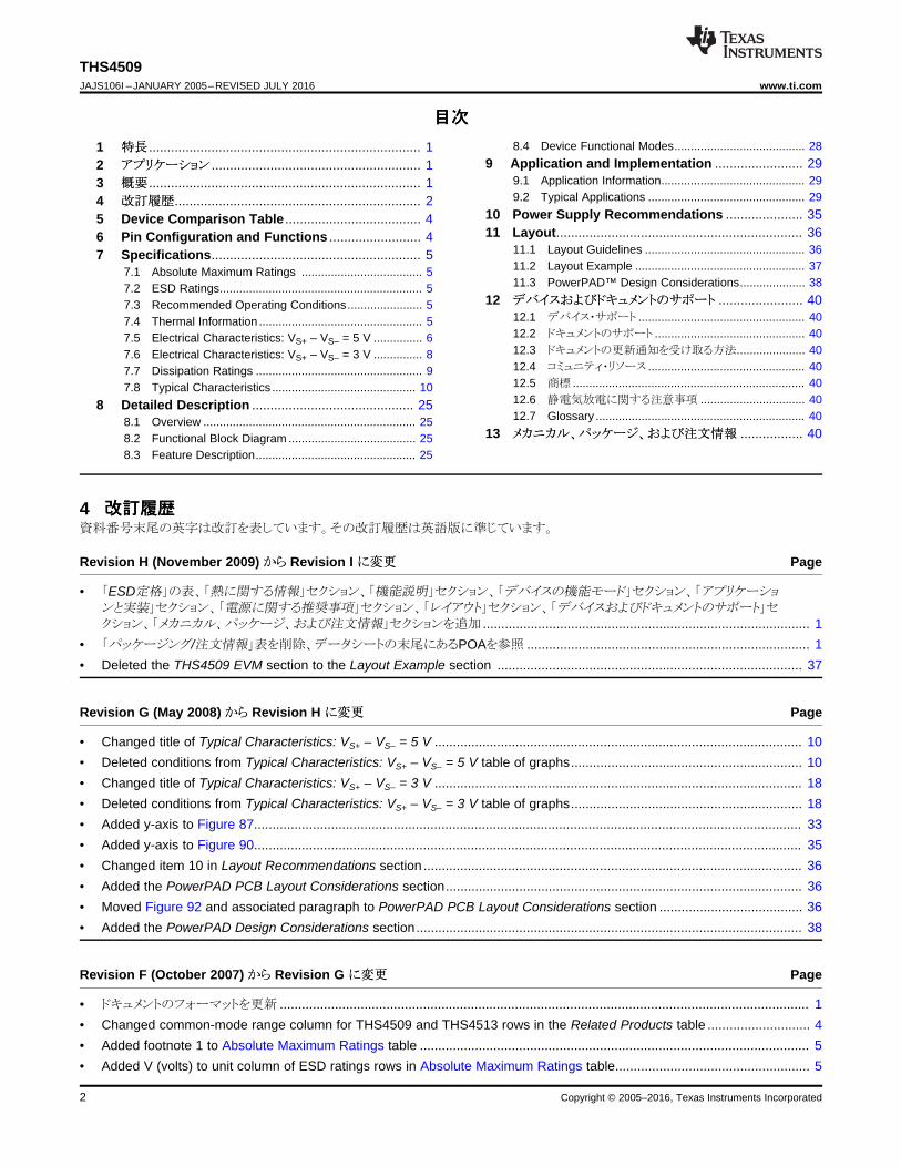
Figure 1. Small-Signal Frequency Response Figure 2. Large-Signal Frequency Response
Figure 3. HD2 vs Frequency Figure 4. HD3 vs Frequency
Figure 5. HD2 vs Frequency Figure 6. HD3 vs Frequency

-110
-100
-90
-50
-40
-30
-1 -0.8 -0.6 -0.4 -0.2 0.4
3rd
Ord
er
Harm
on
ic D
isto
rtio
n−
dB
c
V − − VIC Common-Mode Output Voltage
0 0.2 0.6 10.8
V = -1 V to 1 V
V = 2 V
G = 10 dB
R = 200
CM
OD PP
LW
1 MHz
-120
-80
-60
-70
-20
32 MHz
64 MHz
100 MHz
150 MHz
4 MHz
16 MHz
V = -1 V to 1 V
V = 2 V
G = 10 dB
R = 200
CM
OD PP
LW
32 MHz
100 MHz
64 MHz
16 MHz 4 MHz 1 MHz
-1 -0.8 -0.6 -0.4 -0.2 0.4
V − − VIC Common-Mode Output Voltage
0 0.2 0.6 10.8
-120
-100
-80
-60
-40
-20
0
2n
d O
rder
Harm
on
ic D
isto
rtio
n−
dB
c
150 MHz
-120
-110
-100
-90
-80
-70
-60
0 1 2 3 4
3n
d O
rder
Harm
on
ic D
isto
rtio
n -
dB
c
f = 64 MHz
f = 32 MHz
f = 8 MHz
f = 16 MHz
V - VOD PP
-120
-110
-100
-90
-80
-70
-60
0 1 2 3 4
2n
d-O
rder
Harm
on
ic D
isto
rtio
n -
dB
c
f = 16 MHz
f = 8 MHz
V - VOD PP
f = 64 MHz
f = 32 MHz
−120
−110
−100
−90
−80
−70
−60
1 10 100 1000
f − Frequency − MHz
2n
d O
rder
Harm
on
ic D
isto
rtio
n−
dB
c G = 14 dB,
V = 2 VOD PP
R = 100L W
R = 200L W
R = 1 kL W
R = 500L W
−120
−110
−100
−90
−80
−70
−60
1 10 100 1000
f − Frequency − MHz
3rd
Ord
er H
arm
on
ic D
isto
rti
on
−d
Bc G = 14 dB,
V = 2 VOD PP
R = 100L W
R = 200L W
R = 500L W
R = 1 kL W
12
THS4509JAJS106I –JANUARY 2005–REVISED JULY 2016 www.ti.com
Copyright © 2005–2016, Texas Instruments Incorporated
Figure 7. HD2 vs Frequency Figure 8. HD3 vs Frequency
Figure 9. HD2 vs Output Voltage Figure 10. HD3 vs Output Voltage
Figure 11. HD2 vs Common-Mode Output Voltage Figure 12. HD3 vs Common-Mode Output Voltage

−100
−95
−90
−85
−80
−75
−70
−65
−60
0 50 100 150 200
−In
term
od
ula
tio
n D
isto
rtio
n−
dB
cIM
D3
f − Frequency − MHz
Gain = 14 dBV = 2 V EnvelopeOD PP
R = 100 WL
R = 500 WL
R = 1 kWL
R = 200 WL
−100
−90
−80
−70
−60
−50
−40
−30
0 50 100 150 200
−In
term
od
ula
tio
n D
isto
rtio
n−
dB
cIM
D2
f − Frequency − MHz
R = 1 kL W
R = 200L W
Gain = 14 dB,V = 2 V EnvelopeCO PP
R = 100L W
R = 500L W
0 50 100 150 200
-100
-90
-80
-70
-60
-50
-40
-30
IMD
Inte
rmo
du
lati
on
Dis
tort
ion
dB
c-
-2
f - Frequency MHz-
Gain = 10 dB,V = 2 V Envelope
OD PP
R = 100 WL
R = 200 WL
R = 500 WL
R = 1 kWL
-100
-95
-90
-85
-80
-75
-70
-65
-60
0 50 100 150 200
−In
term
od
ula
tio
n D
isto
rti
on
-d
Bc
IMD
3
F - Frequency - MHz
Gain = 10 dB,V = 2 V EnvelopeOD PP
R = 200L W
R = 100L W
R = 1 kL W
R = 500L W
-100
-95
-90
-85
-80
-75
-70
-65
-60
0 50 100 150 200
IMD
3In
term
od
ula
tio
n D
isto
rtio
nd
Bc
--
f - -Frequency MHz
Gain = 6 dB,V = 2 V Envelope
OD PP
R = 1 kWL
R = 200 WL
R = 100 WL
R = 500 WL
-100
-90
-80
-70
-60
-50
-40
-30
0 50 100 150 200
IMD
Inte
rmo
du
latio
n D
isto
rtio
nd
Bc
-2
-
f Frequency MHz- -
Gain = 6 dB,
V = 2 V EnvelopeOD PPR = 200 WL
R = 100 WL
R = 500 WL
R = 1 kWL
13
THS4509www.ti.com JAJS106I –JANUARY 2005–REVISED JULY 2016
Copyright © 2005–2016, Texas Instruments Incorporated
Figure 13. IMD2 vs Frequency Figure 14. IMD3 vs Frequency
Figure 15. IMD2 vs Frequency Figure 16. IMD3 vs Frequency
Figure 17. IMD2 vs Frequency Figure 18. IMD3 vs Frequency

Tra
nsitio
n R
ate
V/
s-
m
0
1000
2000
3000
4000
5000
6000
7000
8000
0 0.5 1.0 1.5 2.0 2.5 3.0 3.5 4.0
Fall
Rise
V Differential Output Voltage V- -OD STEP
−1.5
−1
−0.5
0
0.5
1
1.5
t − Time − 500 ps/div
VO
D−
Dif
fere
nti
al O
utp
ut
Vo
ltag
e−
V
V = 2 VOD step
9.8
9.9
10
10.1
10.2
0.1 1 10 100 1000
Sig
na
l G
ain
−d
B
f − Frequency − MHz
V = 2VOD PP
1 10 100
-70
-60
-50
-40
-30
-20
-10
0
S-P
ara
me
ters
- d
B
1000
S21
S11
S22
S12
f - Frequency - MHz
40
45
50
55
60
65
70
75
80
85
90
0 50 100 150 200
Gain = 10 dB
−O
utp
ut
Inte
rcep
t P
oin
t−
dB
mO
IP2
f − Frequency − MHz
Gain = 6 dB
Gain = 14 dB
25
27
29
31
33
35
37
39
41
43
45
0 50 100 150 200 250
−O
utp
ut
Inte
rcep
t P
oin
t−
dB
mO
IP3
f − Frequency − MHz
Gain = 6 dB
Gain = 10 dB
Gain = 14 dB
14
THS4509JAJS106I –JANUARY 2005–REVISED JULY 2016 www.ti.com
Copyright © 2005–2016, Texas Instruments Incorporated
Figure 19. OIP2 vs Frequency Figure 20. OIP3 vs Frequency
Figure 21. 0.1-dB Flatness Figure 22. S-Parameters vs Frequency
Figure 23. Transition Rate vs Output Voltage Figure 24. Transient Response

0
1
2
3
4
5
6
7
V-
Dif
fere
nti
al O
utp
ut
Vo
ltag
e -
VO
D
10 100 1000
R - Load Resistance -L W
0
0.4
0.8
1.2
1.6
2
0
1
2
3
4
5
−D
iffe
ren
tial O
up
ut
Vo
ltag
e−
VV
OD
Po
wer
Do
wn
In
pu
t−
V
t − imeT 2 s/divm−
PD
Output
0.1
1
10
100
0.1 1 10 100 1000
f − Frequency− MHz
−O
utp
ut
Imp
ed
an
ce
−Z
oΩ
−5
−4
−3
−2
−1
0
1
2
3
4
5
−1
−0.8
−0.6
−0.4
−0.2
0
0.2
0.4
0.6
0.8
1
Input
Output
VO
D−
Dif
fere
nti
al
Ou
tpu
t V
olt
ag
e−
V
Inpu
t V
olta
ge
−V
t − Time 200 ns/div−
0
10
20
30
40
50
60
70
80
90
100
0.01 0.1 1 10 100 1000
f − Frequency − MHz
Reje
cti
on
Rati
o−
dB
PSRR−
PSRR+
CMRR
−5
−4
−3
−2
−1
0
1
2
3
4
5
t − Time − 500 ps/div
Pe
rce
nt
of
Fin
al
Va
lue
−%
V =2VOD step
15
THS4509www.ti.com JAJS106I –JANUARY 2005–REVISED JULY 2016
Copyright © 2005–2016, Texas Instruments Incorporated
Figure 25. Settling Time Figure 26. Rejection Ratio vs Frequency
Figure 27. Output Impedance vs Frequency Figure 28. Overdrive Recovery
Figure 29. Output Voltage Swing vs Load Resistance Figure 30. Turnoff Time
25
30
35
40
1 1.5 2 2.5
−Q
uie
scen
t C
urr
en
t−
mA
I Q
±1.35 V
T 25 CA
= °
T 5 CA
= 8 °
T CA
= -40°
V - Supply Voltage - VS
10
11
12
13
14
15
16
17
18
19
20
0 50 100 150 200
f − Frequency − MHz
NF
−N
ois
e F
igu
re−
dB
Gain = 10 dB
Gain = 14 dB
Gain = 20 dB
Gain = 6 dB 50 - SystemW
1 100 10 k 1 M 100 M 10 G
Op
en
Lo
op
Gain
−d
B
Op
en
Lo
op
Ph
ase
−d
eg
rees
f − Frequency − Hz
0
10
20
30
40
50
60
70
80
90
-230
-200
-170
-140
-110
-80
-50
-20
10
40
Gain
Phase
nV
/H
z−
Vo
ltag
e N
ois
e−
Vn
I n−
Cu
rren
t N
ois
e−
pA
/H
z
1
10
100
1000
10 100 1 k 10 k 100 k 1 M 10 M
Vn
In
f − Frequency − Hz
−5
0
5
10
15
20
25
30
35
40
−2.5 −2 −1.5 −1 −0.5 0 0.5 1 1.5 2 2.5
Input Common-Mode Voltage − V
VIO
−In
pu
t O
ffset
Vo
ltag
e−
mV
0
0.4
0.8
1.2
1.6
2
t − Time 50 ns/div−
0
1
2
3
4
5
PD
Output
−D
iffe
ren
tial O
utp
ut
Vo
ltag
e−
VV
OD
Po
wer
Do
wn
In
pu
t−
V
16
THS4509JAJS106I –JANUARY 2005–REVISED JULY 2016 www.ti.com
Copyright © 2005–2016, Texas Instruments Incorporated
Figure 31. Turnon Time Figure 32. Input Offset Voltage vs Input Common-ModeVoltage
Figure 33. Open-Loop Gain and Phase vs Frequency Figure 34. Input-Referred Noise vs Frequency
Figure 35. Noise Figure vs Frequency Figure 36. Quiescent Current vs Supply Voltage

−300
−200
−100
0
100
200
300
−2.5 −2 −1.5 −1 −0.5 0 0.5 1 1.5 2 2.5
CM
In
pu
t B
ias C
urr
en
t−
Aµ
CM Input Voltage − V
Dif
fere
nti
al
Ou
tpu
t O
ffs
et
Volt
ag
e−
mV
−1
0
1
2
3
4
5
−2.5 −2 −1.5 −1 −0.5 0 0.5 1 1.5 2 2.5
CM Input Voltage − V
0.1 1 10 100 1000
CM
Gain
−d
B
f − Frequency − MHz
-10
-9
-8
-7
-6
-5
-4
-3
-2
-1
0
1
100 mVPP
CM
In
pu
t Im
pe
da
nc
e−
kΩ
0.01
0.1
1
10
100
0.1 1 10 100 1000
f − Frequency − MHz
0
100
200
300
400
500
600
700
800
0 0.5 1 1.5 2 2.5
Po
wer
Su
pp
ly C
urr
en
t−
Aµ
VS − Supply Voltage − V
TA= 25°C
TA= 85°C
TA= −40°C
−60
−50
−40
−30
−20
−10
0
10
0.1 1 10 100 1000
Ou
tpu
t B
ala
nce E
rro
r−
dB
f − Frequency − MHz
17
THS4509www.ti.com JAJS106I –JANUARY 2005–REVISED JULY 2016
Copyright © 2005–2016, Texas Instruments Incorporated
Figure 37. Power-Supply Current vs Supply Voltage inPower-Down Mode
Figure 38. Output Balance Error vs Frequency
Figure 39. CM Input Impedance vs Frequency Figure 40. CM Small-Signal Frequency Response
Figure 41. CM Input Bias Current vs CM Input Voltage Figure 42. Differential Output Offset Voltage vs CM InputVoltage

−50
−40
−30
−20
−10
0
10
20
30
40
50
−2.5 −2 −1.5 −1 −0.5 0 0.5 1 1.5 2 2.5
Ou
tpu
t C
om
mo
n−
Mo
de
Off
se
t−
mV
CM Input Voltage − V
18
THS4509JAJS106I –JANUARY 2005–REVISED JULY 2016 www.ti.com
Copyright © 2005–2016, Texas Instruments Incorporated
Figure 43. Output Common-Mode Offset vs CM Input Voltage
7.8.2 Typical Characteristics: VS+ – VS– = 3 VTest conditions at VS+ = +1.5 V, VS– = –1.5 V, CM = open, VOD = 1 VPP, RF = 349 Ω, RL = 200-Ω differential, G = 10 dB,single-ended input, and input and output referenced to midrail, unless otherwise noted.
Table 2. Table of GraphsFIGURE
Small-Signal Frequency Response Figure 44Large-Signal Frequency Response Figure 45
HarmonicDistortion
HD2, G = 6 dB, VOD = 1 VPP vs Frequency Figure 46HD3, G = 6 dB, VOD = 1 VPP vs Frequency Figure 47HD2, G = 10 dB, VOD = 1 VPP vs Frequency Figure 48HD3, G = 10 dB, VOD = 1 VPP vs Frequency Figure 49HD2, G = 14 dB, VOD = 1 VPP vs Frequency Figure 50HD3, G = 14 dB, VOD = 1 VPP vs Frequency Figure 51
IntermodulationDistortion
IMD2, G = 6 dB, VOD = 1 VPP vs Frequency Figure 52IMD3, G = 6 dB, VOD = 1 VPP vs Frequency Figure 53IMD2, G = 10 dB, VOD = 1 VPP vs Frequency Figure 54IMD3, G = 10 dB, VOD = 1 VPP vs Frequency Figure 55IMD2, G = 14 dB, VOD = 1 VPP vs Frequency Figure 56IMD3, G = 14 dB, VOD = 1 VPP vs Frequency Figure 57
Output Intercept PointOIP2 vs Frequency Figure 58OIP3 vs Frequency Figure 59
0.1 dB Flatness Figure 60S-Parameters vs Frequency Figure 61Transition Rate vs Output Voltage Figure 62Transient Response Figure 63Settling Time Figure 64Output Voltage Swing vs Load Resistance Figure 65Rejection Ratio vs Frequency Figure 66Overdrive Recovery Figure 67Output Impedance vs Frequency Figure 68Turnoff Time Figure 69Turnon Time Figure 70Output Balance Error vs Frequency Figure 71Noise Figure vs Frequency Figure 72CM Input Impedance vs Frequency Figure 73

−120
−110
−100
−90
−80
−70
−60
−50
−40
1 10 100 1000
f − Frequency − MHz
2n
d O
rder
Harm
on
ic D
isto
rtio
n−
dB
c
R L= 500 Ω
R L= 200Ω
R L= 1 kΩ
G = 10 dB,
V = 1 VOD PP
−100
−90
−80
−70
−60
−50
−40
1 10 100 1000
f − Frequency − MHz
3rd
Ord
er
Ha
rmo
nic
Dis
tort
ion
−d
Bc G = 10 dB,
C = 1 VOD PP
R = 1 kL W
R = 200L W
R = 500L W
-120
-110
-100
-90
-80
-70
-60
-50
-40
1 10 100 1000
f - -Frequency MHz
2n
dO
rder
Harm
on
ic D
isto
rtio
nd
Bc
-
G = 6 dB,
V = 1 VOD PP
R = 100 WL
R = 200 WL R = 1 kW
L
R = 500 WL
f − Frequency − MHz
3rd
Ord
er
Ha
rmo
nic
Dis
tort
ion
−d
Bc
−100
−90
−80
−70
−60
−50
−40
1 10 100 1000
R = 1 kL W
R = 500L W
R = 200L W
R = 100L W
G = 6 dB,
V = 1 VOD PP
Sm
all S
ign
al G
ain
−d
B
0
2
4
6
8
10
12
14
16
18
20
22
0.1 1 10 100 1000 10000
f - Frequency - MHz
V = 100 mVOD PP
G = 20 dB
G = 14 dB
G = 10 dB
G = 6 dB
0
2
4
6
8
10
12
14
16
18
20
22
0.1 1 10 100 1000 10000
f− Frequency − MHz
Larg
e S
ign
al G
ain
−d
B
V = 1 VOD PP
G = 20 dB
G = 14 dB
G = 10 dB
G = 6 dB
19
THS4509www.ti.com JAJS106I –JANUARY 2005–REVISED JULY 2016
Copyright © 2005–2016, Texas Instruments Incorporated
Typical Characteristics: VS+ – VS– = 3 V (continued)Table 2. Table of Graphs (continued)
FIGUREDifferential Output Offset Voltage vs CM Input Voltage Figure 74Output Common-Mode Offset vs CM Input Voltage Figure 75
Figure 44. Small-Signal Frequency Response Figure 45. Large-Signal Frequency Response
Figure 46. HD2 vs Frequency Figure 47. HD3 vs Frequency
Figure 48. HD2 vs Frequency Figure 49. HD3 vs Frequency
−100
−90
−80
−70
−60
−50
−40
−30
0 50 100 150 200
f − Frequency − MHz
−In
term
od
ula
tio
n D
isto
rtio
n−
dB
cIM
D2
Gain = 10 dB,V = 1 V EnvelopeOD PP
R = 500L W
R = 1 kL W
R = 200L W
R = 100L W
-100
-90
-80
-70
-60
-50
-40
-30
05 0 100 150 200
IMD
3In
term
od
ula
tio
n-
Dis
tort
ion
dB
c-
f - -Frequency MHz
Gain = 10 dB,V = 1 V Envelope
OD PP
R = 100 WL
R = 1 kWL
R = 500 WL
R = 200 WL
−In
term
od
ula
tio
n D
isto
rtio
n−
dB
cIM
D2
−100
−90
−80
−70
−60
−50
−40
−30
0 50 100 150 200
f − Frequency − MHz
R = 500L W
R = 200L W
R = 100L W
R = 1 kL W
Gain = 6 dB,
V = 1 VOD PP
−100
−90
−80
−70
−60
−50
−40
−30
0 50 100 150 200
−In
term
od
ula
tio
n D
isto
rtio
n−
dB
cIM
D3
f − Frequency − MHz
Gain = 6 dB,V = 1 V EnvelopeOD PP
R = 100L W
R = 1 kL W
R = 500L W
R = 200L W
−120
−110
−100
−90
−80
−70
−60
−50
−40
1 10 100 1000
f − Frequency − MHz
2n
d O
rd
er H
arm
on
ic D
isto
rti
on
−d
Bc
R L= 500 Ω
R L= 200Ω
R L= 100Ω
G = 14 dB,
V = 1 VOD PP
R L= 1 k Ω
−100
−90
−80
−70
−60
−50
−40
1 10 100 1000
f − Frequency − MHz
3rd
Ord
er
Harm
on
ic D
isto
rtio
n−
dB
c
R = 500L W
R = 1 kL W
R = 200L W
R = 100L W
G = 14 dB,
V = 1 VOD PP
20
THS4509JAJS106I –JANUARY 2005–REVISED JULY 2016 www.ti.com
Copyright © 2005–2016, Texas Instruments Incorporated
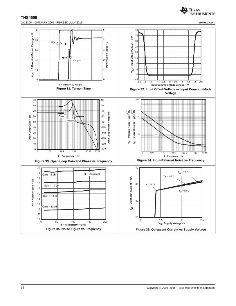
Figure 50. HD2 vs Frequency Figure 51. HD3 vs Frequency
Figure 52. IMD2 vs Frequency Figure 53. IMD3 vs Frequency
Figure 54. IMD2 vs Frequency Figure 55. IMD3 vs Frequency

-70
-60
-50
-40
-30
-20
-10
0
1 10 100 1000
f = Frequency - MHz
S-P
ara
mete
rs -
dB
S21
S11
S22
S12
Sig
nal G
ain
−d
B
f − Frequency − MHz
9.8
9.9
10
10.1
10.2
0.1 1 10 100 1000 10000
V = 1 VOD PP
30
35
40
45
50
55
60
65
70
75
80
0 50 100150 200
−O
utp
ut
Inte
rcep
t P
oin
t−
dB
mO
IP2
Gain = 6 dB
f − Frequency − MHz
Gain = 10 dB
Gain = 14 dB
15
20
25
30
35
40
45
0 50 100 150 200 250
−O
utp
ut
Inte
rcep
t P
oin
t−
dB
mO
IP3
f − Frequency − MHz
Gain = 10 dB
Gain = 14 dB
Gain = 6 dB
−100
−90
−80
−70
−60
−50
−40
−30
0 50 100 150 200
f − Frequency − MHz
−In
term
od
ula
tio
n D
isto
rtio
n−
dB
cIM
D2
Gain = 14 dB,V = 1 V EnvelopeOD PP
R = 500L W
R = 200L W
R = 1 kL WR = 100L W
−100
−90
−80
−70
−60
−50
−40
−30
0 50 100 150 200
−In
term
od
ula
tio
n D
isto
rtio
n−
dB
cIM
D3
f − Frequency − MHz
Gain = 14 dB,V = 1 V EnvelopeOD PP
R = 100L W
R = 500L W
R = 1 kL W
R = 200L W
21
THS4509www.ti.com JAJS106I –JANUARY 2005–REVISED JULY 2016
Copyright © 2005–2016, Texas Instruments Incorporated
Figure 56. IMD2 vs Frequency Figure 57. IMD3 vs Frequency
Figure 58. OIP2, dBm vs Frequency Figure 59. OIP3, dBm vs Frequency
Figure 60. 0.1-dB Flatness Figure 61. S-Parameters vs Frequency

f − Frequency − MHz
Reje
cti
on
Rati
o−
dB
0
10
20
30
40
50
60
70
80
90
0.01 0.1 1 10 100 1000
CMRR
PSRR−
PSRR+
VO
D−
Dif
fere
nti
al
Ou
tpu
t V
olt
ag
e -
V
Inp
ut
Vo
lta
ge
- V
t − Time 200 ns/div−
−3
−2.5
−2
−1.5
−1
−0.5
0
0.5
1
1.5
2
2.5
3
−0.6
−0.4
−0.2
0
0.2
0.4
0.6
Input
Output
0
0.5
1
1.5
2
2.5
0 100 1000
V-
Dif
fere
nti
alO
utp
ut
Vo
ltag
e-
VO
D
R - Load Resistance -L W
−5
−4
−3
−2
−1
0
1
2
3
4
5
t − Time 500 ps/div−
Perc
en
t o
f F
inal V
olt
ag
e -
V
V = 1 VOD step
VOD − Differential Output Voltage - VSTEP
SR
−Tra
ns
itio
n R
ate
−V
/s
µ
0
500
1000
1500
2000
2500
3000
3500
4000
0 0.2 0.4 0.6 0.8 1 1.2 1.4
Falling
Rising
−0.6
−0.5
−0.4
−0.3
−0.2
−0.1
0
0.1
0.2
0.3
0.4
0.5
0.6
t − Time − 500 ps/div
VO
D−
Dif
fere
nti
al O
utp
ut
Vo
ltag
e -
V
V = 1 VOD step
22
THS4509JAJS106I –JANUARY 2005–REVISED JULY 2016 www.ti.com
Copyright © 2005–2016, Texas Instruments Incorporated
Figure 62. Transition Rate vs Output Voltage Figure 63. Transient Response
Figure 64. Settling Time Figure 65. Output Voltage Swing vs Load Resistance
Figure 66. Rejection Ratio vs Frequency Figure 67. Overdrive Recovery

10
11
12
13
14
15
16
17
18
19
20
0 50 100 150 200
f − Frequency − MHz
NF
−N
ois
e F
igu
re−
dB
50 - SystemWGain = 6 dB
Gain = 10 dB
Gain = 14 dB
Gain = 20 dB
CM
In
pu
t Im
ped
an
ce
−k
Ω
f − Frequency − MHz
0.01
0.1
1
10
100
0.1 1 10 100 1000
Ou
tpu
t B
ala
nce E
rro
r−
dB
f − Frequency − MHz
−60
−50
−40
−30
−20
−10
0
10
0.1 1 10 100 1000
t − Time − 50 ns/div
Po
we
r D
ow
n I
np
ut
−V
0
0.2
0.4
0.6
0.8
1
1.2
0
0.5
1
1.5
2
2.5
3
V-
-D
iffe
ren
tia
l O
utp
ut
Vo
lta
ge
VO
D
PD
Ou tp u t
f − Frequency− MHz
−O
utp
ut
Imp
ed
an
ce
−Z
oΩ
0.1
1
10
100
0.1 1 10 100 1000
−D
iffe
ren
tial O
up
ut
Vo
ltag
e -
VV
OD
Po
wer
Do
wn
In
pu
t−
V
0
0.2
0.4
0.6
0.8
1
0
0.5
1
1.5
2
2.5
3
t – Time 2 s/divm–
PD
Output
23
THS4509www.ti.com JAJS106I –JANUARY 2005–REVISED JULY 2016
Copyright © 2005–2016, Texas Instruments Incorporated
Figure 68. Output Impedance vs Frequency Figure 69. Turnoff Time
Figure 70. Turnon Time Figure 71. Output Balance Error vs Frequency
Figure 72. Noise Figure vs Frequency Figure 73. CM Input Impedance vs Frequency

Dif
fere
nti
al O
utp
ut
Off
set
Vo
ltag
e−
mV
CM Input Voltage − V
−1
0
1
2
3
4
5
−1.5 −1 −0.5 0 0.5 1 1.5
−50
−40
−30
−20
−10
0
10
20
30
40
50
−1.5 −1 −0.5 0 0.5 1 1.5
Ou
tpu
t C
om
mo
n−
Mo
de O
ffset
−m
V
CM Input Voltage - V
24
THS4509JAJS106I –JANUARY 2005–REVISED JULY 2016 www.ti.com
Copyright © 2005–2016, Texas Instruments Incorporated
Figure 74. Differential Output Offset Voltage vs CM InputVoltage
Figure 75. Output Common-Mode Offset vs CM InputVoltage

V+
-IN
+
±
High-AolDifferential I/OAmplifier
+IN
50 k
10 k
10 k
+OUT
-OUT
+
±
+
±VcmError
AmplifierVcm
V+
50 k
EN Buffer
V±Copyright © 2016, Texas Instruments Incorporated
25
THS4509www.ti.com JAJS106I –JANUARY 2005–REVISED JULY 2016
Copyright © 2005–2016, Texas Instruments Incorporated
8 Detailed Description
8.1 OverviewThe THS4509 is a fully differential amplifier with integrated common-mode control designed to provide lowdistortion amplification to wide bandwidth differential signals. The common-mode feedback circuit sets the outputcommon-mode voltage independent of the input common mode, as well as forcing the V+ and V − outputs to beequal in magnitude and opposite in phase, even when only one of the inputs is driven as in single to differentialconversion.
8.2 Functional Block Diagram
8.3 Feature Description
8.3.1 Test CircuitsThe THS4509 is tested with the following test circuits built on the evaluation module (EVM). For simplicity,power-supply decoupling is not shown—see Layout for recommendations. Depending on the test conditions,component values are changed per Table 3 and Table 4, or as otherwise noted. The signal generators used areAC-coupled, 50-Ω sources, and a 0.22-μF capacitor and 49.9-Ω resistor to ground are inserted across RIT on thealternate input to balance the circuit. A split power supply is used to ease the interface to common testequipment, but the amplifier can be operated single-supply as described in Typical Applications with no impacton performance.
Output MeasuredHere With HighImpedanceDifferential Probe
THS4509
CM
VIN RF
RF
RG
RG
RIT
RIT
From50 Ω
Source VS+
VS−
49.9 Ω
49.9 Ω100 Ω
0.22 Fµ
49.9 Ω 0.22 Fµ
Open
Copyright © 2016, Texas Instruments Incorporated
26
THS4509JAJS106I –JANUARY 2005–REVISED JULY 2016 www.ti.com
Copyright © 2005–2016, Texas Instruments Incorporated
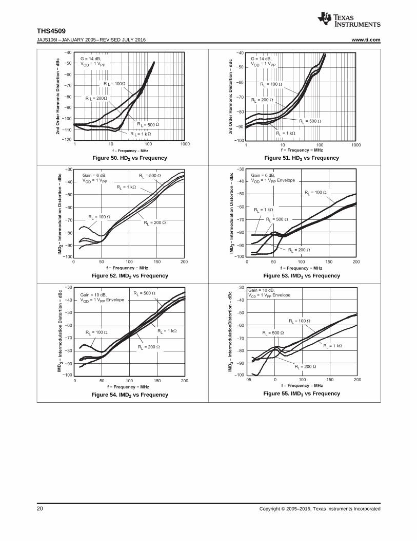
Feature Description (continued)Table 3. Gain Component Values
GAIN RF RG RIT
6 dB 348 Ω 165 Ω 61.9 Ω10 dB 348 Ω 100 Ω 69.8 Ω14 dB 348 Ω 56.2 Ω 88.7 Ω20 dB 348 Ω 16.5 Ω 287 Ω
Note the gain setting includes 50-Ω source impedance. Components are chosen to achieve gain and 50-Ωinput termination.
Table 4. Load Component ValuesRL RO ROT ATTEN.
100 Ω 25 Ω Open 6 dB200 Ω 86.6 Ω 69.8 Ω 16.8 dB499 Ω 237 Ω 56.2 Ω 25.5 dB1k Ω 487 Ω 52.3 Ω 31.8 dB
Note the total load includes 50-Ω termination by the test equipment. Components are chosen to achieveload and 50-Ω line termination through a 1:1 transformer.Due to the voltage divider on the output formed by the load component values, the amplifier output is attenuated.The column Atten in Table 4 shows the attenuation expected from the resistor divider. When using a transformerat the output as shown in Figure 77, the signal sees slightly more loss, and these numbers are approximate.
8.3.1.1 Frequency ResponseThe circuit shown in Figure 76 is used to measure the frequency response of the circuit.
Figure 76. Frequency Response Test Circuit
A network analyzer is used as the signal source and as the measurement device. The output impedance of thenetwork analyzer is 50 Ω. RIT and RG are chosen to impedance match to 50 Ω, and to maintain the proper gain.To balance the amplifier, a 0.22-μF capacitor and 49.9-Ω resistor to ground are inserted across RIT on thealternate input.
The output is probed using a high-impedance differential probe across the 100-Ω resistor. The gain is referred tothe amplifier output by adding back the 6-dB loss due to the voltage divider on the output.
8.3.1.2 Distortion and 1-dB CompressionThe circuit shown in Figure 77 is used to measure harmonic distortion, intermodulation distortion, and 1-dbcompression point of the amplifier.

THS 4509
CM
VIN RF
RF
RG
RG
RIT
RIT
From50 Ω
Source
0.22 Fµ
49.9 Ω
VOUT+
Open
To 50 ΩTestEquipment
VS+
VS−
0.22 Fµ
VOUT−
49.9 Ω
49.9 Ω
Copyright © 2016, Texas Instruments Incorporated
THS 4509
CM
From50 Ω
Source
VIN
0.22 Fµ
49.9 Ω
VOUT
Open
To 50 ΩTestEquipment
RG
RIT
RG
RIT
RF
VS+
VS−
RO
ROROT
0.22 Fµ
1:1
RF
Copyright © 2016, Texas Instruments Incorporated
27
THS4509www.ti.com JAJS106I –JANUARY 2005–REVISED JULY 2016
Copyright © 2005–2016, Texas Instruments Incorporated
Feature Description (continued)
Figure 77. Distortion Test Circuit
A signal generator is used as the signal source and the output is measured with a spectrum analyzer. The outputimpedance of the signal generator is 50 Ω. RIT and RG are chosen to impedance-match to 50 Ω, and to maintainthe proper gain. To balance the amplifier, a 0.22-μF capacitor and 49.9-Ω resistor to ground are inserted acrossRIT on the alternate input.
A low-pass filter is inserted in series with the input to reduce harmonics generated at the signal source. The levelof the fundamental is measured, then a high-pass filter is inserted at the output to reduce the fundamental so thatit does not generate distortion in the input of the spectrum analyzer.
The transformer used in the output to convert the signal from differential to single-ended is an ADT1-1WT. Itlimits the frequency response of the circuit so that measurements cannot be made below approximately 1 MHz.
The 1-dB compression point is measured with a spectrum analyzer with 50-Ω double termination or 100-Ωtermination; see Table 4. The input power is increased until the output is 1 dB lower than expected. The numberreported in the table data is the power delivered to the spectrum analyzer input. Add 3 dB to refer to the amplifieroutput.
8.3.1.3 S-Parameter, Slew Rate, Transient Response, Settling Time, Output Impedance, Overdrive,Output Voltage, Turnon, and Turnoff Time
The circuit shown in Figure 78 is used to measure s-parameters, slew rate, transient response, settling time,output impedance, overdrive recovery, output voltage swing, turnon, and turnoff times of the amplifier. For outputimpedance, the signal is injected at VOUT with VIN left open and the drop across the 49.9-Ω resistor is used tocalculate the impedance seen looking into the amplifier output.
Because S21 is measured single-ended at the load with 50-Ω double termination, add 12 dB to refer to theamplifier output as a differential signal.
Figure 78. S-Parameter, SR, Transient Response, Settling Time, ZO, Overdrive Recovery, VOUT Swing,Turnon, and Turnoff Test Circuit

From50 Ω
Source THS4509
CM
VIN
CMRR
PSRR+
PSRR−
VS+
VS−
VS+
VS−
100 Ω
100 Ω
69.8 Ω
348 Ω
348 Ω
49.9 Ω
49.9 Ω
Open
0.22 Fµ
100 Ω
OutputMeasuredHereWith HighImpedanceDifferentialProbe
Copyright © 2016, Texas Instruments Incorporated
VS+
CMVIN From
source
VS–49.9 W
0.22 Fm
RF
RF
RG
RG
RIT
RIT
VOUT+
VOUT–
To
50-WTest
Equipment
RCMT
RCM
THS4509
50-W
49.9 W
0.22 Fm
49.9 W
49.9 W
Copyright © 2016, Texas Instruments Incorporated
28
THS4509JAJS106I –JANUARY 2005–REVISED JULY 2016 www.ti.com
Copyright © 2005–2016, Texas Instruments Incorporated
Feature Description (continued)8.3.1.4 CM InputThe circuit shown in Figure 79 is used to measure the frequency response and input impedance of the CM input.Frequency response is measured single-ended at VOUT+ or VOUT– with the input injected at VIN, RCM = 0 Ω, andRCMT = 49.9 Ω. The input impedance is measured with RCM = 49.9 Ω with RCMT = open, and calculated bymeasuring the voltage drop across RCM to determine the input current.
Figure 79. CM Input Test Circuit
8.3.1.5 CMRR and PSRRThe circuit shown in Figure 80 is used to measure the CMRR and PSRR of VS+ and VS–. The input is switchedappropriately to match the test being performed.
Figure 80. CMRR and PSRR Test Circuit
8.4 Device Functional ModesThe THS4509 has one main functional mode with two variants. The amplifier functions as either a differential todifferential or a single-ended to differential amplifier. In either of these modes the amplifier output operating point(common-mode voltage) is set independently by the CM pin.
The THS4509 also features a power-down state for reduced power consumption when the amplifier is notrequired to be operational.

RF
VOUT+
VOUT–
VS+
VIN–
VS–
RF
RG
RG
VIN+
THS4509
DifferentialInput
DifferentialOutput
+ –
– +
Copyright © 2016, Texas Instruments Incorporated
29
THS4509www.ti.com JAJS106I –JANUARY 2005–REVISED JULY 2016
Copyright © 2005–2016, Texas Instruments Incorporated
9 Application and Implementation
NOTEInformation in the following applications sections is not part of the TI componentspecification, and TI does not warrant its accuracy or completeness. TI’s customers areresponsible for determining suitability of components for their purposes. Customers shouldvalidate and test their design implementation to confirm system functionality.
9.1 Application InformationThe THS4509 is a fully-configurable, differential operational amplifier. The closed-loop gain is set by externalresistors. Many performance metrics are set by the matching of these external resistors, so 0.1% or bettertolerance resistors are recommended.
The amplifier output common-mode voltage is set by the CM pin. From the CM pin to the amplifier outputs thereis a fixed gain of 1 V/V so that the amplifier output voltage is identical to the voltage applied to the CM pin. Thispin must be driven by a low impedance reference and must also be bypassed to ground using a 0.1-µF ceramic,low ESR resistor. The ideal common-mode voltage is equal to the voltage that is midway between the positiveand negative supply voltages.
The THS4509 can be operated from either single or split power supplies with a range of 3 V to 5 V of total supplyvoltage. When selecting a power supply voltage, make sure to provide adequate margin for input and outputvoltage levels. In many cases, split supplies are the best option. It is not necessary to have power supplyvoltages symmetrical around ground. For example, –1 V and +4 V is a valid power supply configuration.
9.2 Typical ApplicationsThe following circuits show application information for the THS4509. For simplicity, power-supply decouplingcapacitors are not shown in these diagrams. See the Layout section for recommendations. For more detail on theuse and operation of fully-differential op amps refer to the application report, Fully-Differential Amplifiers(SLOA054).
9.2.1 Differential Input to Differential Output AmplifierThe THS4509 is a fully-differential op amp, and can be used to amplify differential input signals to differentialoutput signals. A basic block diagram of the circuit is shown in Figure 81 (CM input not shown). The gain of thecircuit is set by RF divided by RG.
Depending on the source and load, input and output termination can be accomplished by adding RIT and RO.
Figure 81. Differential Input to Differential-Output Amplifier
9.2.1.1 Design RequirementsThe following sections detail how to determine if your design meets these requirements.

( )W
--= -+
k50
VVV2I
SSCM
EXT
÷÷ø
öççè
æ
+´+÷
÷ø
öççè
æ
+´= -+
FG
F
IN
FG
G
OUTICRR
RV
RR
RVV
30
THS4509JAJS106I –JANUARY 2005–REVISED JULY 2016 www.ti.com
Copyright © 2005–2016, Texas Instruments Incorporated
Typical Applications (continued)The main design requirements for the THS4509 are the input common mode, the output swing voltage. Otherdesign requirements are signal linearity and accuracy. With flexible supply voltage ranges and externallyconfigurable resistors the THS4509 can be configured to meet many design requirements.
Table 5 lists the design parameters of this example.
Table 5. Design ParametersPARAMETER EXAMPLE VALUE
Gain 6 dBOutput swing 2 Vpp
Harmonic distortion >75 dBcLoad resistance 100 Ω
9.2.1.2 Detailed Design ProcedureThe first parameter is gain. Gain is set by external resistors as shown in Table 3. With a gain of 6 dB, theappropriate resistor values are 348 Ω for RF and 165 Ω for RG and 61.9 Ω for the termination resistor. Theseresistor values are for a 50-Ω source. The desired output swing of 2 Vpp and distortion of –75 dBc means that asupply voltage of 5 V is required. Further design details are covered in this section.
9.2.1.2.1 Input Common-Mode Voltage Range
The input common-mode voltage of a fully-differential op amp is the voltage at the + and – input pins of the opamp.
It is important to not violate the input common-mode voltage range (VICR) of the op amp. Assuming the op amp isin linear operation the voltage across the input pins is only a few millivolts at most. So finding the voltage at oneinput pin determines the input common-mode voltage of the op amp.
Treating the negative input as a summing node, the voltage is given by Equation 1:
(1)
To determine the VICR of the op amp, the voltage at the negative input is evaluated at the extremes of VOUT+.
As the gain of the op amp increases, the input common-mode voltage becomes closer and closer to the inputcommon-mode voltage of the source.
9.2.1.2.2 Setting the Output Common-Mode Voltage
The output common-mode voltage is set by the voltage at the CM pin(s). The internal common-mode controlcircuit maintains the output common-mode voltage within 3-mV offset (typical) from the set voltage, when setwithin 0.5 V of midsupply, with less than 4-mV differential offset voltage. If left unconnected, the common-modeset point is set to midsupply by internal circuitry, which may be overdriven from an external source. Figure 82 isrepresentative of the CM input. The internal CM circuit has about 700 MHz of –3-dB bandwidth, which is requiredfor best performance, but it is intended to be a DC bias input pin. Bypass capacitors are recommended on thispin to reduce noise at the output. The external current required to overdrive the internal resistor divider is givenby Equation 2:
where• VCM is the voltage applied to the CM pin (2)

( )
÷÷ø
öççè
æ+-÷÷
ø
öççè
æ
-= +
FIN
IC
F
CM
SIC
PU
R
1
R
1V
R
1V
VVR
VS+
CM
VSignal
VS–
RF
RF
RG
RG
RT
RO
RO
VOUT+
VOUT-
THS4509VBias= VCM
RS
RT
VCM
VCM
VCM
VCM
RS
Copyright © 2016, Texas Instruments Incorporated
VS+
CM
VS–
50 kW
to internal
CM circuit
IEXT
50 kW
31
THS4509www.ti.com JAJS106I –JANUARY 2005–REVISED JULY 2016
Copyright © 2005–2016, Texas Instruments Incorporated
Figure 82. CM Input Circuit
9.2.1.2.3 Single-Supply Operation (3 V to 5 V)
To facilitate testing with common lab equipment, the THS4509 EVM allows split-supply operation, and thecharacterization data presented in this data sheet were taken with split-supply power inputs. The device caneasily be used with a single-supply power input without degrading the performance. Figure 83, Figure 84, andFigure 85 show DC and AC-coupled single-supply circuits with single-ended inputs. These configurations allallow the input and output common-mode voltage to be set to midsupply allowing for optimum performance. Theinformation presented here can also be applied to differential input sources.
In Figure 83, the source is referenced to the same voltage as the CM pin (VCM). VCM is set by the internal circuitto midsupply. RT along with the input impedance of the amplifier circuit provides input termination, which is alsoreferenced to VCM.
NOTERS and RT are added to the alternate input from the signal input to balance the amplifier.Alternately, one resistor can be used equal to the combined value RG+ RS || RT on thisinput. This is also true of the circuits shown in Figure 84 and Figure 85.
Figure 83. THS4509 DC-Coupled Single-Supply With Input Biased to VCM
In Figure 84 the source is referenced to ground and so is the input termination resistor. RPU is added to thecircuit to avoid violating the VICR of the op amp. The proper value of resistor to add can be calculated fromEquation 3:
(3)

VS+=3V to 5V
CM
V Signal
VS-
R F
R F
R G
R G
R T
R O
R O
VOUT+
VOUT-
THS 4509
C
RS
R T
C
C
RS
C
VS+
CM
VSignal
VS-
RF
RF
RG
RG
RT
RO
RO
VOUT+
VOUT-
THS 4509
RS
RTRS
VS+
VS+
RPU
RPU
Copyright © 2016, Texas Instruments Incorporated
32
THS4509JAJS106I –JANUARY 2005–REVISED JULY 2016 www.ti.com
Copyright © 2005–2016, Texas Instruments Incorporated
Figure 84. THS4509 DC-Coupled Single-Supply With RPU Used to Set VIC
VIC is the desired input common-mode voltage, VCM = CM, and RIN = RG+ RS || RT. To set to midsupply, makethe value of RPU = RG+ RS || RT.
Table 6 is a modification of Table 3 to add the proper values with RPU assuming a 50-Ω source impedance andsetting the input and output common-mode voltage to midsupply.
Table 6. RPU Values for Various GainsGAIN RF RG RIT RPU
6 dB 348 Ω 169 Ω 64.9 Ω 200 Ω10 dB 348 Ω 102 Ω 78.7 Ω 133 Ω14 dB 348 Ω 61.9 Ω 115 Ω 97.6 Ω20 dB 348 Ω 40.2 Ω 221 Ω 80.6 Ω
There are two drawbacks to this configuration. One is that it requires additional current from the power supply.Using the values shown for a gain of 10 dB requires 37 mA more current with 5-V supply, and 22-mA morecurrent with 3-V supply.
The other drawback is that this configuration also increases the noise gain of the circuit. In the 10-dB gain case,noise gain increases by a factor of 1.5.
Figure 85 shows AC coupling to the source. Using capacitors in series with the termination resistors allows theamplifier to self-bias both input and output to midsupply.
Figure 85. THS4509 AC-Coupled Single-Supply
65
70
75
80
85
90
10 20 30 40 50 60 70 80 90 100 110
Input Frequency - MHz
SFDR (dBc)
SNR (dBFS)
SF
DR
(d
Bc),
SN
R (
dB
FS
)
2.7 pF
0.1 Fm
14-bit,
125 MSPS
A IN +
A IN - CM
ADS5500
4 V
THS 4509
CM
348 W
348 W
100 W
100 W
69.3 W
VINFrom
50-source
W
100 W
100 W
-1 V69.8 W 49.9 W
0.22 Fm
49.9 W
0.22 Fm0.22 Fm 0.1 Fm
Copyright © 2016, Texas Instruments Incorporated
33
THS4509www.ti.com JAJS106I –JANUARY 2005–REVISED JULY 2016
Copyright © 2005–2016, Texas Instruments Incorporated
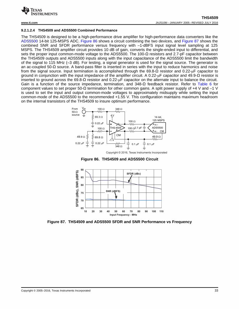
9.2.1.2.4 THS4509 and ADS5500 Combined Performance
The THS4509 is designed to be a high-performance drive amplifier for high-performance data converters like theADS5500 14-bit 125-MSPS ADC. Figure 86 shows a circuit combining the two devices, and Figure 87 shows thecombined SNR and SFDR performance versus frequency with –1-dBFS input signal level sampling at 125MSPS. The THS4509 amplifier circuit provides 10 dB of gain, converts the single-ended input to differential, andsets the proper input common-mode voltage to the ADS5500. The 100-Ω resistors and 2.7-pF capacitor betweenthe THS4509 outputs and ADS5500 inputs along with the input capacitance of the ADS5500 limit the bandwidthof the signal to 115 MHz (–3 dB). For testing, a signal generator is used for the signal source. The generator isan ac-coupled 50-Ω source. A band-pass filter is inserted in series with the input to reduce harmonics and noisefrom the signal source. Input termination is accomplished through the 69.8-Ω resistor and 0.22-μF capacitor toground in conjunction with the input impedance of the amplifier circuit. A 0.22-μF capacitor and 49.9-Ω resistor isinserted to ground across the 69.8-Ω resistor and 0.22-μF capacitor on the alternate input to balance the circuit.Gain is a function of the source impedance, termination, and 348-Ω feedback resistor. Refer to Table 6 forcomponent values to set proper 50-Ω termination for other common gains. A split power supply of +4 V and –1 Vis used to set the input and output common-mode voltages to approximately midsupply while setting the inputcommon-mode of the ADS5500 to the recommended +1.55 V. This configuration maintains maximum headroomon the internal transistors of the THS4509 to insure optimum performance.
Figure 86. THS4509 and ADS5500 Circuit
Figure 87. THS4509 and ADS5500 SFDR and SNR Performance vs Frequency

.2 7pF
0.1 Fm
14-bit,
105 MSPS
A IN+
A IN– VBG
ADS5424
5 V
THS4509
CM
348 W
348 W
100 W
100
69.8 W
VINFrom
50-source
W
225 W
225 W
69.8 W 49.9 W49.9 W
0.22 Fm 0.22 Fm0.1 Fm
0.22 Fm
Copyright © 2016, Texas Instruments Incorporated
34
THS4509JAJS106I –JANUARY 2005–REVISED JULY 2016 www.ti.com
Copyright © 2005–2016, Texas Instruments Incorporated
Figure 88 shows the two-tone FFT of the THS4509 and ADS5500 circuit with 65-MHz and 70-MHz inputfrequencies. The SFDR is 90 dBc.
Figure 88. THS4509 and ADS5500 2-Tone FFT With 65-MHz and 70-MHz Inputs
9.2.1.2.5 THS4509 and ADS5424 Combined Performance
Figure 89 shows the THS4509 driving the ADS5424 ADC, and Figure 90 shows the combined SNR and SFDRperformance versus frequency with –1-dBFS input signal level and sampling at 80 MSPS.
As before, the THS4509 amplifier provides 10 dB of gain, converts the single-ended input to differential, and setsthe proper input common-mode voltage to the ADS5424. Input termination and circuit testing is the same asdescribed above for the THS4509 and ADS5500 circuit.
The 225-Ω resistors and 2.7-pF capacitor between the THS4509 outputs and ADS5424 inputs (along with theinput capacitance of the ADC) limit the bandwidth of the signal to about 100MHz (–3 dB).
Because the ADS5424 recommended input common-mode voltage is 2.4 V, the THS4509 is operated from asingle power-supply input with VS+ = 5 V and VS– = 0 V (ground).
Figure 89. THS4509 and ADS5424 Circuit

VS
Single-EndedInput
VS
RF
RF
RG
RGTHS4509
Differential
Output
VOUT+
VOUT–+
–
–
+
Copyright © 2016, Texas Instruments Incorporated
70
75
80
85
90
95
10 20 30 40 50 60 70
Input Frequency - MHz
SFDR (dBc)
SNR (dBFS)
SF
DR
(d
Bc),
SN
R (
dB
FS
)
35
THS4509www.ti.com JAJS106I –JANUARY 2005–REVISED JULY 2016
Copyright © 2005–2016, Texas Instruments Incorporated
9.2.1.3 Application Curve
Figure 90. THS4509 and ADS5424 SFDR and SNR Performance vs Frequency
9.2.2 Single-Ended Input to Differential Output AmplifierThe THS4509 can be used to amplify and convert single-ended input signals to differential output signals. Abasic block diagram of the circuit is shown in Figure 91 (CM input not shown). The gain of the circuit is again setby RF divided by RG.
Figure 91. Single-Ended Input to Differential Output Amplifier
10 Power Supply RecommendationsThe THS4509 can accommodate supply voltages from 3 V to 5 V, either single supply or split supply. Unless theapplication calls for AC coupling and a very small signal the 5-V supply option must be chosen. In many cases,split supplies are necessary because it is important to have the output common-mode voltage set very close tothe midsupply voltage. For example, when driving an ADC with an input common-mode voltage of 1 V the idealpower supply voltage would be +3.5 V and –1.5 V.
Power supply decoupling capacitors must be placed within 2 mm of the amplifier power supply pins. Thesecapacitors must be very low ESR and must have a self resonant frequency above 200 mHz.
36
THS4509JAJS106I –JANUARY 2005–REVISED JULY 2016 www.ti.com
Copyright © 2005–2016, Texas Instruments Incorporated
11 Layout
11.1 Layout GuidelinesIt is recommended to follow the layout of the external components near the amplifier, ground plane construction,and power routing of the EVM as closely as possible.
11.1.1 General Guidelines1. Signal routing should be direct and as short as possible into and out of the op amp circuit.2. The feedback path should be short and direct; avoid vias.3. Ground or power planes should be removed from directly under the amplifier input and output pins.4. An output resistor is recommended on each output, as near to the output pin as possible.5. Two 10-μF and two 0.1-μF power-supply decoupling capacitors must be placed as near to the power-supply
pins as possible.6. Two 0.1-μF capacitors must be placed between the CM input pins and ground. This configuration limits noise
coupled into the pins. One each must be placed to ground near pin 4 and pin 9.7. TI recommends splitting the ground panel on layer 2 (L2) as shown below and to use a solid ground on layer
3 (L3). A single-point connection must be used between each split section on L2 and L3.8. A single-point connection to ground on L2 is recommended for the input termination resistors R1 and R2.
This configuration must be applied to the input gain resistors if termination is not used.9. The THS4509 recommended PCB footprint is shown in Figure 92.
11.1.2 PowerPAD PCB Layout ConsiderationsAlthough there are many ways to properly heatsink the PowerPAD package, the following steps illustrate therecommended approach:1. Prepare the PCB with a top side etch pattern as shown in Figure 92. There must be etch for the leads as
well as etch for the thermal pad.2. Place five holes in the area of the thermal pad. The holes must be 13 mils (0.013 in, 0.33 mm) in diameter.
Keep them small so that solder wicking through the holes is not a problem during reflow.3. Additional vias may be placed anywhere along the thermal plane outside of the thermal pad area. They help
dissipate the heat generated by the IC. These additional vias may be larger than the 13-mil diameter viasdirectly under the thermal pad. They can be larger because they are not in the thermal pad area to besoldered, so that wicking is not a problem.
4. Connect all holes to the internal ground plane.5. When connecting these holes to the ground plane, do not use the typical web or spoke via connection
methodology. Web connections have a high thermal resistance connection that is useful for slowing the heattransfer during soldering operations. This resistance makes the soldering of vias that have plane connectionseasier. In this application, however, low thermal resistance is desired for the most efficient heat transfer.Therefore, the holes under the IC PowerPAD package should make the connection to the internal groundplane, with a complete connection around the entire circumference of the plated-through hole.
6. The top-side solder mask must leave the terminals of the package and the thermal pad area with its fiveholes exposed. The bottom-side solder mask should cover the five holes of the thermal pad area. Thisconfiguration prevents solder from being pulled away from the thermal pad area during the reflow process.
7. Apply solder paste to the exposed thermal pad area and all of the IC terminals.8. With these preparatory steps in place, the IC is simply placed in position and run through the solder reflow
operation as any standard surface-mount component. This process results in a part that is properly installed.
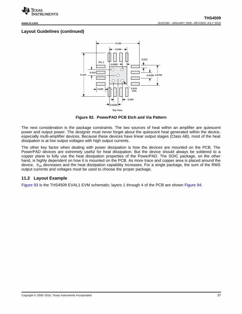
0.144 0.0195
0.144
0.010vias
Pin 1
Top View
0.012
0.030
0.07050.015
0.0095
0.049
0.032
0.0245
37
THS4509www.ti.com JAJS106I –JANUARY 2005–REVISED JULY 2016
Copyright © 2005–2016, Texas Instruments Incorporated
Layout Guidelines (continued)
Figure 92. PowerPAD PCB Etch and Via Pattern
The next consideration is the package constraints. The two sources of heat within an amplifier are quiescentpower and output power. The designer must never forget about the quiescent heat generated within the device,especially multi-amplifier devices. Because these devices have linear output stages (Class AB), most of the heatdissipation is at low output voltages with high output currents.
The other key factor when dealing with power dissipation is how the devices are mounted on the PCB. ThePowerPAD devices are extremely useful for heat dissipation. But the device should always be soldered to acopper plane to fully use the heat dissipation properties of the PowerPAD. The SOIC package, on the otherhand, is highly dependent on how it is mounted on the PCB. As more trace and copper area is placed around thedevice, θJA decreases and the heat dissipation capability increases. For a single package, the sum of the RMSoutput currents and voltages must be used to choose the proper package.
11.2 Layout ExampleFigure 93 is the THS4509 EVAL1 EVM schematic; layers 1 through 4 of the PCB are shown Figure 94.

49.9 Ω
−
+
J1
R12 C15
0.22 µF
R169.8 Ω
R3
100 Ω
R4
100 Ω
R269.8 Ω
J2
TP2
C140.1 Fµ
C110.1 Fµ
TP1
U1 11
2
12
4
Vocm
9
TP3
R6
348 Ω
131514 16
PwrPad10
VO−
VO+
3
7586
VCC348 Ω
VCC
R5
PD
C9
0.1 µF
C10
0.1 µF
C4
10 µF 10 µF
C6
VEE
VS−
J4 J5
GND
VEE
VS+
J6
C3
10 µF 10 µF
C5
0.1 µF 0.1 µF
C12 C13
J8
J3T1
16
5
4
R9
open
R7
86.6 Ω
R8
86.6 Ω
R10open
XFMR_ADT1−1WT
3
R11
69.8 Ω
J7
C8
open
C7
open
C1open
C2
open
VCC
VEE
38
THS4509JAJS106I –JANUARY 2005–REVISED JULY 2016 www.ti.com
Copyright © 2005–2016, Texas Instruments Incorporated
Figure 93. THS4509 EVAL1 EVM Schematic
Figure 94. THS4509 EVAL1 EVM Layer 1 Through Layer 4
11.3 PowerPAD™ Design ConsiderationsThe THS4509 is available in a thermally-enhanced PowerPAD family of packages. These packages areconstructed using a downset leadframe on which the die is mounted (see Figure 95a and Figure 95b). Thisarrangement results in the lead frame being exposed as a thermal pad on the underside of the package (seeFigure 95c). Because this thermal pad has direct thermal contact with the die, excellent thermal performance canbe achieved by providing a good thermal path away from the thermal pad.
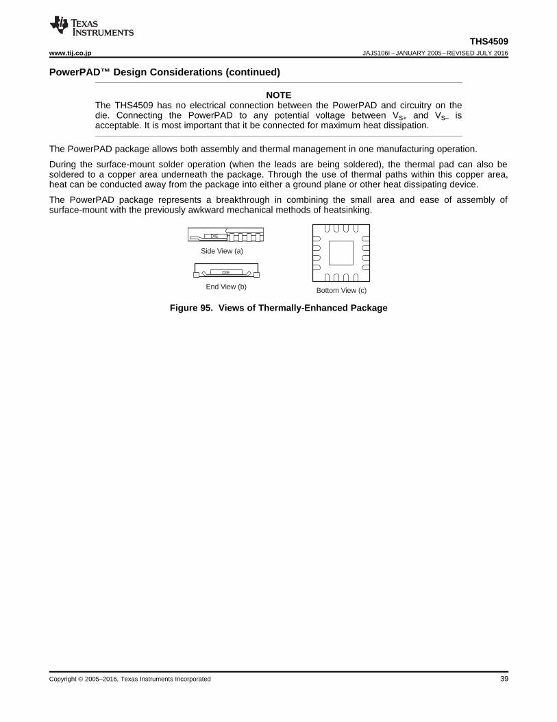
DIE
Side View (a)
DIE
End View (b) Bottom View (c)
39
THS4509www.tij.co.jp JAJS106I –JANUARY 2005–REVISED JULY 2016
Copyright © 2005–2016, Texas Instruments Incorporated
PowerPAD™ Design Considerations (continued)
NOTEThe THS4509 has no electrical connection between the PowerPAD and circuitry on thedie. Connecting the PowerPAD to any potential voltage between VS+ and VS– isacceptable. It is most important that it be connected for maximum heat dissipation.
The PowerPAD package allows both assembly and thermal management in one manufacturing operation.
During the surface-mount solder operation (when the leads are being soldered), the thermal pad can also besoldered to a copper area underneath the package. Through the use of thermal paths within this copper area,heat can be conducted away from the package into either a ground plane or other heat dissipating device.
The PowerPAD package represents a breakthrough in combining the small area and ease of assembly ofsurface-mount with the previously awkward mechanical methods of heatsinking.
Figure 95. Views of Thermally-Enhanced Package
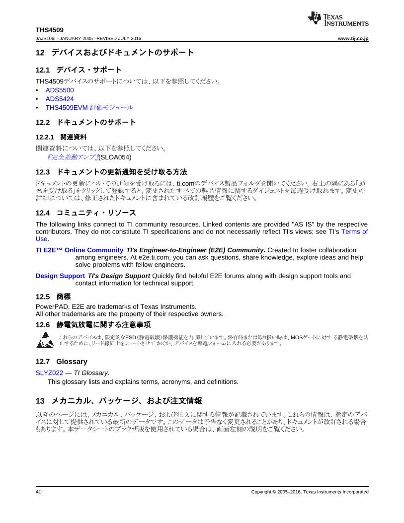
40
THS4509JAJS106I –JANUARY 2005–REVISED JULY 2016 www.tij.co.jp
Copyright © 2005–2016, Texas Instruments Incorporated
12 デデババイイススおおよよびびドドキキュュメメンントトののササポポーートト
12.1 デデババイイスス・・ササポポーートトTHS4509デバイスのサポートについては、以下を参照してください。
• ADS5500• ADS5424• THS4509EVM 評価モジュール
12.2 ドドキキュュメメンントトののササポポーートト
12.2.1 関関連連資資料料関連資料については、以下を参照してください。
『完全差動アンプ』(SLOA054)
12.3 ドドキキュュメメンントトのの更更新新通通知知をを受受けけ取取るる方方法法ドキュメントの更新についての通知を受け取るには、ti.comのデバイス製品フォルダを開いてください。右上の隅にある「通知を受け取る」をクリックして登録すると、変更されたすべての製品情報に関するダイジェストを毎週受け取れます。変更の詳細については、修正されたドキュメントに含まれている改訂履歴をご覧ください。
12.4 ココミミュュニニテティィ・・リリソソーーススThe following links connect to TI community resources. Linked contents are provided "AS IS" by the respectivecontributors. They do not constitute TI specifications and do not necessarily reflect TI's views; see TI's Terms ofUse.
TI E2E™ Online Community TI's Engineer-to-Engineer (E2E) Community. Created to foster collaborationamong engineers. At e2e.ti.com, you can ask questions, share knowledge, explore ideas and helpsolve problems with fellow engineers.
Design Support TI's Design Support Quickly find helpful E2E forums along with design support tools andcontact information for technical support.
12.5 商商標標PowerPAD, E2E are trademarks of Texas Instruments.All other trademarks are the property of their respective owners.
12.6 静静電電気気放放電電にに関関すするる注注意意事事項項これらのデバイスは、限定的なESD(静電破壊)保護機能を内 蔵しています。保存時または取り扱い時は、MOSゲートに対す る静電破壊を防止するために、リード線同士をショートさせて おくか、デバイスを導電フォームに入れる必要があります。
12.7 GlossarySLYZ022 — TI Glossary.
This glossary lists and explains terms, acronyms, and definitions.
13 メメカカニニカカルル、、パパッッケケーージジ、、おおよよびび注注文文情情報報以降のページには、メカニカル、パッケージ、および注文に関する情報が記載されています。これらの情報は、指定のデバイスに対して提供されている最新のデータです。このデータは予告なく変更されることがあり、ドキュメントが改訂される場合もあります。本データシートのブラウザ版を使用されている場合は、画面左側の説明をご覧ください。

PACKAGE OPTION ADDENDUM
www.ti.com 11-Aug-2016
Addendum-Page 1
PACKAGING INFORMATION
Orderable Device Status(1)
Package Type PackageDrawing
Pins PackageQty
Eco Plan(2)
Lead/Ball Finish(6)
MSL Peak Temp(3)
Op Temp (°C) Device Marking(4/5)
Samples
THS4509RGTR ACTIVE QFN RGT 16 3000 Green (RoHS& no Sb/Br)
CU NIPDAU Level-2-260C-1 YEAR -40 to 85 4509
THS4509RGTRG4 ACTIVE QFN RGT 16 3000 Green (RoHS& no Sb/Br)
CU NIPDAU Level-2-260C-1 YEAR -40 to 85 4509
THS4509RGTT ACTIVE QFN RGT 16 250 Green (RoHS& no Sb/Br)
CU NIPDAU Level-2-260C-1 YEAR -40 to 85 4509
THS4509RGTTG4 ACTIVE QFN RGT 16 250 Green (RoHS& no Sb/Br)
CU NIPDAU Level-2-260C-1 YEAR -40 to 85 4509
(1) The marketing status values are defined as follows:ACTIVE: Product device recommended for new designs.LIFEBUY: TI has announced that the device will be discontinued, and a lifetime-buy period is in effect.NRND: Not recommended for new designs. Device is in production to support existing customers, but TI does not recommend using this part in a new design.PREVIEW: Device has been announced but is not in production. Samples may or may not be available.OBSOLETE: TI has discontinued the production of the device.
(2) Eco Plan - The planned eco-friendly classification: Pb-Free (RoHS), Pb-Free (RoHS Exempt), or Green (RoHS & no Sb/Br) - please check http://www.ti.com/productcontent for the latest availabilityinformation and additional product content details.TBD: The Pb-Free/Green conversion plan has not been defined.Pb-Free (RoHS): TI's terms "Lead-Free" or "Pb-Free" mean semiconductor products that are compatible with the current RoHS requirements for all 6 substances, including the requirement thatlead not exceed 0.1% by weight in homogeneous materials. Where designed to be soldered at high temperatures, TI Pb-Free products are suitable for use in specified lead-free processes.Pb-Free (RoHS Exempt): This component has a RoHS exemption for either 1) lead-based flip-chip solder bumps used between the die and package, or 2) lead-based die adhesive used betweenthe die and leadframe. The component is otherwise considered Pb-Free (RoHS compatible) as defined above.Green (RoHS & no Sb/Br): TI defines "Green" to mean Pb-Free (RoHS compatible), and free of Bromine (Br) and Antimony (Sb) based flame retardants (Br or Sb do not exceed 0.1% by weightin homogeneous material)
(3) MSL, Peak Temp. - The Moisture Sensitivity Level rating according to the JEDEC industry standard classifications, and peak solder temperature.
(4) There may be additional marking, which relates to the logo, the lot trace code information, or the environmental category on the device.
(5) Multiple Device Markings will be inside parentheses. Only one Device Marking contained in parentheses and separated by a "~" will appear on a device. If a line is indented then it is a continuationof the previous line and the two combined represent the entire Device Marking for that device.
(6) Lead/Ball Finish - Orderable Devices may have multiple material finish options. Finish options are separated by a vertical ruled line. Lead/Ball Finish values may wrap to two lines if the finishvalue exceeds the maximum column width.

PACKAGE OPTION ADDENDUM
www.ti.com 11-Aug-2016
Addendum-Page 2
Important Information and Disclaimer:The information provided on this page represents TI's knowledge and belief as of the date that it is provided. TI bases its knowledge and belief on informationprovided by third parties, and makes no representation or warranty as to the accuracy of such information. Efforts are underway to better integrate information from third parties. TI has taken andcontinues to take reasonable steps to provide representative and accurate information but may not have conducted destructive testing or chemical analysis on incoming materials and chemicals.TI and TI suppliers consider certain information to be proprietary, and thus CAS numbers and other limited information may not be available for release.
In no event shall TI's liability arising out of such information exceed the total purchase price of the TI part(s) at issue in this document sold by TI to Customer on an annual basis.
OTHER QUALIFIED VERSIONS OF THS4509 :
• Automotive: THS4509-Q1
NOTE: Qualified Version Definitions:
• Automotive - Q100 devices qualified for high-reliability automotive applications targeting zero defects

TAPE AND REEL INFORMATION
*All dimensions are nominal
Device PackageType
PackageDrawing
Pins SPQ ReelDiameter
(mm)
ReelWidth
W1 (mm)
A0(mm)
B0(mm)
K0(mm)
P1(mm)
W(mm)
Pin1Quadrant
THS4509RGTR QFN RGT 16 3000 330.0 12.4 3.3 3.3 1.1 8.0 12.0 Q2
THS4509RGTT QFN RGT 16 250 180.0 12.4 3.3 3.3 1.1 8.0 12.0 Q2
PACKAGE MATERIALS INFORMATION
www.ti.com 12-Aug-2016
Pack Materials-Page 1

*All dimensions are nominal
Device Package Type Package Drawing Pins SPQ Length (mm) Width (mm) Height (mm)
THS4509RGTR QFN RGT 16 3000 367.0 367.0 35.0
THS4509RGTT QFN RGT 16 250 210.0 185.0 35.0
PACKAGE MATERIALS INFORMATION
www.ti.com 12-Aug-2016
Pack Materials-Page 2

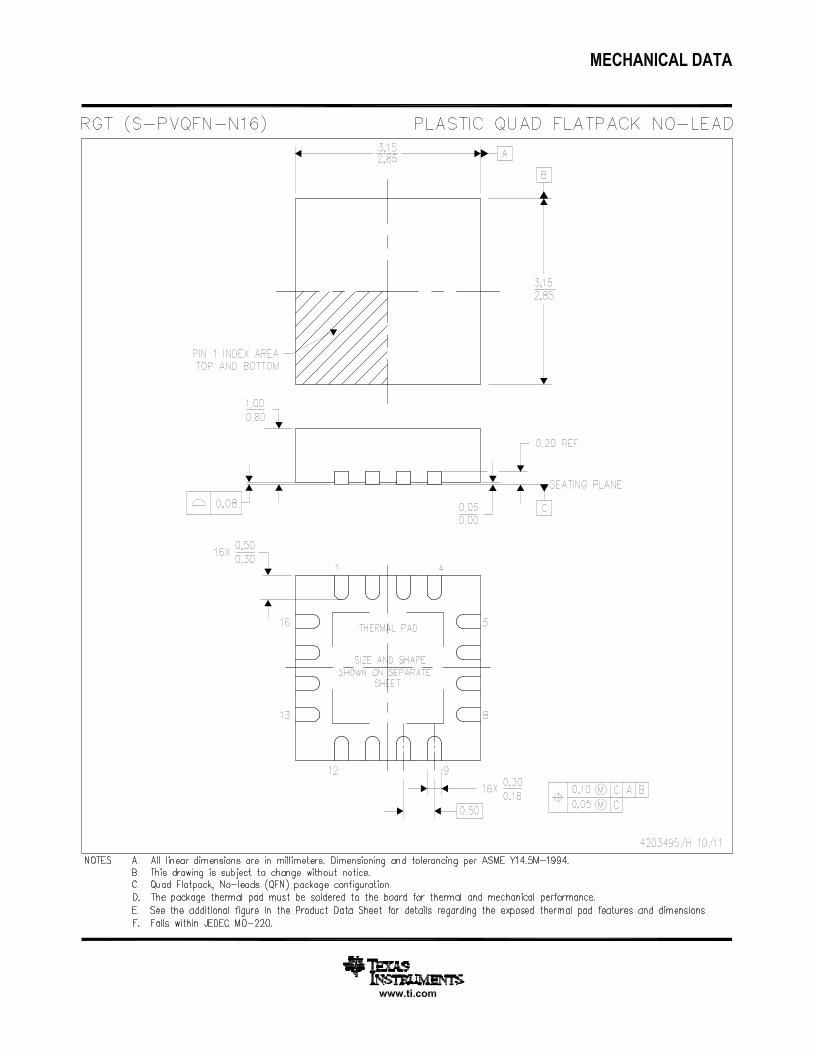
IMPORTANT NOTICE重重要要ななおお知知ららせせ
Texas Instruments Incorporated (TI)は、JESD46の最新版に従って自社の半導体製品およびサービスに訂正、拡張、改良、および、その他の変更を加える権利と、JESD48の最新版に従って任意の製品またはサービスを打ち切る権利を留保します。購入者は発注を行う前に、最新の関連情報を取得し、それらの情報が最新かつ完全なものであることを確認する義務があります。
TIの半導体製品に関する公開済みの販売条項(http://www.tij.co.jp/general/jp/docs/gencontent.tsp?contentId=27309)は、TIが認定し、市場へリリースしたパッケージ集積回路製品の販売に適用されます。他の種類のTI製品およびサービスの使用または販売については、追加条項が適用される場合があります。
TIデータシートに記載されているTI情報の重要な部分の複製は、その情報に一切の変更を加えることなく、かつ、その情報に関連するすべての保証、条件、制限、通知が付属する場合のみ許可されます。このような複製文書について、TIは一切の責任または義務を負いません。第三者の情報については、さらに別の制限が課される可能性があります。TI製品またはサービスの再販において、その製品またはサービスについてTIが規定したパラメータと異なるか、それを超える記述を付すことは不公正かつ欺瞞的な商慣習であり、そのような場合、関連するTI製品またはサービスに関する明示的および黙示的な保証のすべてが無効となります。このような記述について、TIは一切責任または義務を負いません。
購入者、およびTI製品を組み込んだシステムを開発する他者(以下、「設計者」と総称します)は、自らのアプリケーションの設計において、独自の分析、評価、判断を行う責任は設計者自身にあること、および、設計者のアプリケーション(および、設計者のアプリケーションに使用されるすべてのTI製品)の安全性、および該当するすべての規制、法、その他適用される要件の遵守を保証するすべての責任は設計者のみが負うことを理解し、同意するものとします。設計者は、自身のアプリケーションに関して、(1) 危険な不具合から生じる結果を予期し、(2) 不具合およびその結果を監視し、また、(3) 害を及ぼす不具合の可能性を低減するため、保全策を策定および実施し、かつ、適切な是正措置を講じるうえで必要な専門的知識を持つことを表明するものとします。設計者は、TI製品を含むいずれかのアプリケーションを使用または配布する前に、そのアプリケーション、および、アプリケーションで使用されるTI製品の機能を完全にテストすることに同意するものとします。
TIの技術、アプリケーションまたはその他の設計に関する助言、品質特性、信頼性のデータ、もしくは、他のサービスまたは情報は、TI製品を組み込んだアプリケーションを開発する設計者に役立つことを目的として提供するものです。これにはリファレンス設計や、評価モジュールに関係する資料が含まれますが、これらに限られません(以下、これらを総称して「TIリソース」とします)。いかなる方法であっても、TIリソースのいずれかをダウンロード、アクセス、または使用した場合、設計者(個人、または会社を代表している場合には設計者の会社)は、TIリソースをここに記載された目的にのみ使用し、この注意事項の条項に従うことに同意したものとします。
TIによるTIリソースの提供は、TI製品に対する該当の発行済み保証事項または免責事項を、拡張、またはどのような形でも変更するものではなく、これらのTIリソースを提供することによって、TIにはいかなる追加義務または責任も発生しません。TIは、自社のTIリソースに訂正、拡張、改良、および、その他の変更を加える権利を留保します。TIは、特定のTIリソース用に発行されたドキュメントで明示的に記載されている以外のテストを実行していません。
設計者は、個別のTIリソースを、そのTIリソースに記載されているTI製品を搭載したアプリケーションの開発に関連する目的でのみ、使用、複製、および改変することが認められています。明示または黙示を問わず、禁反言の法理その他どのような理由でも、他のTIの知的所有権に対するその他のライセンスは与えられず、ITまたはいかなる第三者のテクノロジまたは知的所有権についても、いかなるライセンスも与えるものではありません。これには、TI製品またはサービスが使用される組み合わせ、機械、またはプロセスに関連する特許権、著作権、回路配置利用権、その他の知的所有権が含まれますが、これらに限られません。第三者の製品やサービスに関する、またはそれらを参照する情報は、そのような製品またはサービスを利用するライセンスを構成するものではなく、それらに対する保証または推奨を意味するものでもありません。TIリソースを使用するため、第三者の特許または他の知的所有権に基づく第三者からのライセンス、もしくは、TIの特許または他の知的所有権に基づくTIからのライセンスが必要な場合があります。
TIのリソースは、それに含まれるあらゆる欠陥も含めて、「現状のまま」提供されます。TIは、TIリソースまたはその使用に関して、明示か黙示かにかかわらず、他のいかなる保証または表明も行いません。これには、正確性または完全性、権原、続発性の障害に関する保証、ならびに、商品性、特定目的への適合性、および、第三者の知的所有権の非侵害に対する黙示の保証が含まれますが、これらに限られません。TIは、設計者への弁護または補償を行う義務はなく、行わないものとします。これには、任意の製品の組み合わせに関する、または、それらに基づく侵害の請求も含まれますが、これらに限られず、また、その事実についてTIリソースまたはその他の場所に記載されているか否かを問わないものとします。いかなる場合も、TIリソースまたはその使用に関連して、またはそれらにより発生した、実際、直接的、特別、付随的、間接的、懲罰的、偶発的、または、結果的な損害について、そのような損害の可能性についてTIが知らされていたか否かにかかわらず、TIは責任を負わないものとします。
TIが特定の業界標準(例えば、ISO/TS 16949およびISO 26262を含む。)の要求に適合していることを明示的に指定した個々の本製品でない限り、TIは、業界標準の要求事項を満たしていなかったことについて、いかなる責任も負いません 。
TIが製品について、機能的安全性の促進、または業界の機能的安全性基準の遵守を特に推進している場合、そのような製品は、お客様が該当の機能的安全性基準および要件を満たすアプリケーションを自ら設計および製作するために役立てることを意図したものです。アプリケーションにこれらの製品を使用することのみで、アプリケーションの安全性が確立されるものではありません。設計者は、自らのアプリケーションについて、該当する安全性関連の要件および基準の遵守を保証する必要があります。設計者は、安全でないことが致命的となる医療機器にTI製品を使用してはいけません。但し、両当事者の権限のある役員間で、かかる使用について具体的に規定した特別な契約が締結された場合はその限りではありません。安全でないことが致命的となる医療機器とは、かかる機器の不具合が重大な身体的障害又は死亡を引き起こすものを指し、生命維持装置、ペースメーカー、除細動器、心臓マッサージ機、神経刺激装置および移植医療機器を含みます。かかる機器には米国の食品医薬品局(FDA)がクラスIIIに指定するもの、また、米国外で同等に分類されているものを含みますがこれらに限られません。
TIは、特定の本製品が特別な品質(Q100、軍需対応グレード品、機能強化製品を例とする。)を満たしていることを明示的に指定することがあります。設計者は、自らのアプリケーションに適した品質が確保された本製品を選択するために必要な専門的知識を持ち、かつ、本製品の選択は買主の責任で行うことに同意するものとします。設計者は、かかる選択に関連して、法規制で要求される事項を遵守する責任を単独で負うものとします。
設計者は、自らがこのお知らせの条項および条件に従わなかったために発生した、いかなる損害、コスト、損失、責任からも、TIおよびその代表者を完全に免責するものとします。
Copyright © 2017, Texas Instruments Incorporated日本語版 日本テキサス・インスツルメンツ株式会社