three-dimensionaland2.5dimensional...
TRANSCRIPT
Three-Dimensional and 2.5 Dimensional
Interconnection Technology: State of
the Art
Dapeng LiuMechanical Engineering,
State University of New York at Binghamton,
P.O. Box 6000,
Binghamton, NY 13902
e-mail: [email protected]
Seungbae Park1
Mechanical Engineering,
State University of New York at Binghamton,
P.O. Box 6000,
Binghamton, NY 13902
e-mail: [email protected]
Three-dimensional (3D) packaging with through-silicon-vias(TSVs) is an emerging technology featuring smaller package size,higher interconnection density, and better performance; 2.5Dpackaging using silicon interposers with TSVs is an incrementalstep toward 3D packaging. Formation of TSVs and interconnec-tion between chips and/or wafers are two key enabling technolo-gies for 3D and 2.5D packaging, and different interconnectionmethods in chip-to-chip, chip-to-wafer, and wafer-to-waferschemes have been developed. This article reviews state-of-the-artinterconnection technologies reported in recent technical papers.Issues such as bump formation, assembly/bonding process, as wellas underfill dispensing in each interconnection type are discussed.[DOI: 10.1115/1.4026615]
1 Introduction
In recent years, driven by the demand for new electronic prod-ucts with smaller size, lower power consumption, and better per-formance, 3D packaging is attracting more and more attentionfrom academia and industry. Traditional electronics are integratedin the 2D scheme, and in the early days, usually only one chipwas encapsulated in a package. Later, the system in package (SiP)technology brought several chips into a single package, whichincreases the speed while reducing the size of the package.
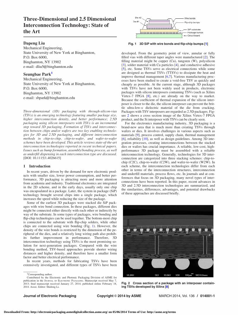
Some of the earliest 3D packages were stacked die SiP pack-ages with wire bond connection. In these packages, different diesmight be connected either directly with each other or indirectly byway of the substrate. In some types of packages, wire bonding andflip-chip technologies can be used together. The bottom-most chipis connected to the substrate with flip-chip solders, while otherchips are connected using wire bonding (Fig. 1). However, thedensity of the wire bonds is restricted by the dimension of the pe-ripheral of the dies, and a relatively long wiring path also prohib-its further improvement in performance. Therefore, 3Dinterconnection technology using TSVs is the most promising so-lution for next-generation packages. Compared with the wirebonding method, TSV-based approaches provide shorter wiringdistances and higher density, and therefore have a smaller formfactor and better electrical performance.
In recent years, methods for fabricating TSVs have beenextensively investigated, and different types of TSVs have been
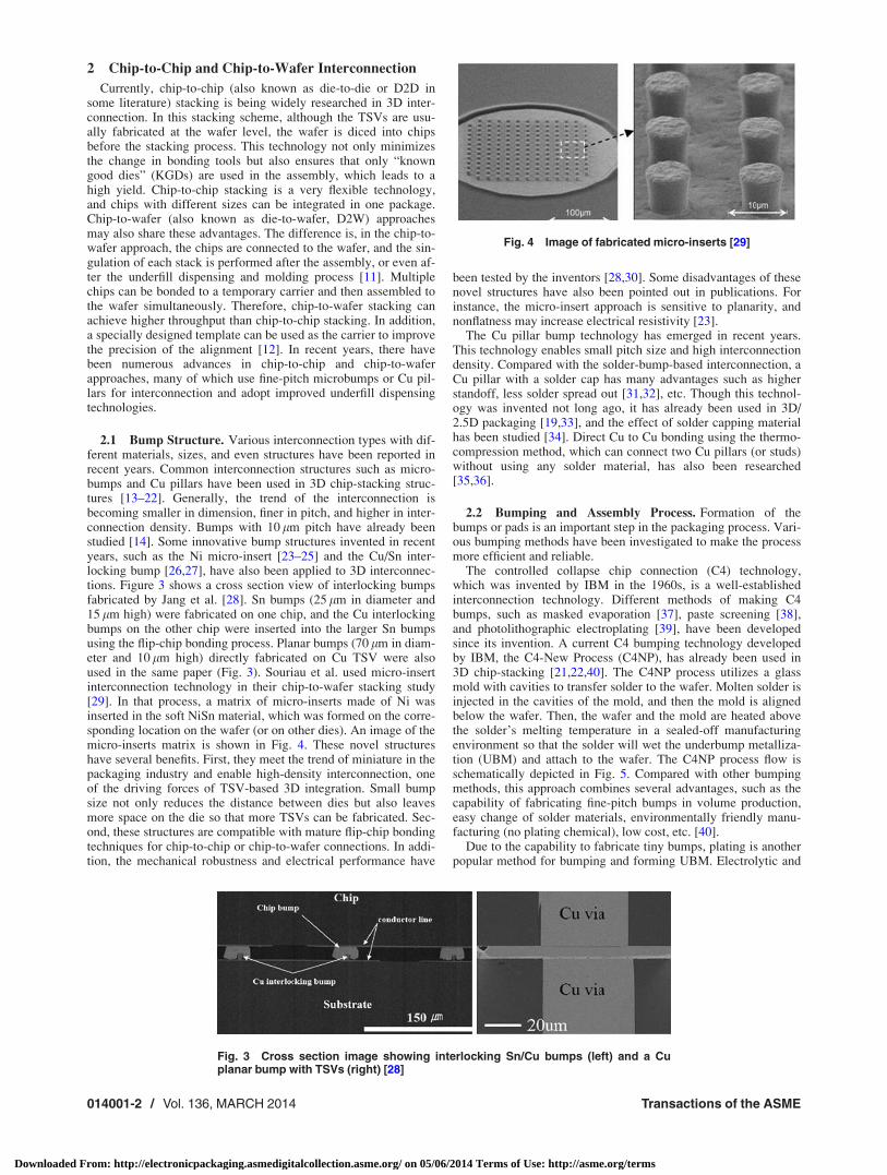
developed. From the geometry point of view, annular or fullyfilled vias with different taper angles were manufactured [2]. Thefilling material might be copper (Cu), tungsten (W), polysilicon[3], solder material with Cu particles [4], and conductive adhesive[5], etc. Some TSVs serve as electrical connections while someare designed as thermal TSVs (TTSVs) to dissipate the heat andimprove thermal management [6,7]. Various manufacturing proc-esses have been studied to create a void-free TSV as quickly andcheaply as possible. At the current stage, although 3D packageswith TSVs have not been widely used in products, electronicpackages with silicon interposers containing TSVs (such as XilinxVirtex-7 FPGA [8], etc.) are already on the way to market.Because the coefficient of thermal expansion of the silicon inter-poser is closer to the die, the silicon interposer can prevent the brit-tle ultra-low-j dielectric material of the die from cracking.Packages with TSV interposers are regarded as 2.5D packages. Fig-ure 2 shows a cross section image of the Xilinx Virtex-7 FPGAproduct, and the Si interposer with TSVs can be clearly seen.
For the electronics manufacturing industry, 3D packaging is abrand-new area that is much more than creating TSVs throughwafers or dies. It involves challenges in various aspects such asmaterials [9], process control, supply chain, thermal management[6], reliability [10], as well as design guidelines. Among 3D inte-gration processes, creating interconnections between the stackeddies or wafers has crucial importance. A reliable, low-cost, high-performance 3D package must be assembled with a reliableinterconnection technology. Generally, technologies for 3D inter-connection are categorized into three stacking schemes: chip-to-chip (C2C), chip-to-wafer (C2W), and wafer-to-wafer (W2W). Ineach scheme, the interconnection technologies differ from eachother in terms of the interconnection structures, interconnectionand underfill materials, process flows, etc. In journals and at con-ferences that focus on 3D packaging, many novel types of inter-connections have been reported. In this paper, recent advances in3D and 2.5D interconnection technologies are summarized, andthe similarities, differences, advantages, and potential drawbacksof these approaches are discussed briefly.
Fig. 1 3D SiP with wire bonds and flip-chip bumps [1]
Fig. 2 Cross section of a package with an interposer contain-ing TSVs developed by Xilinx [8]
1Corresponding author.Contributed by the Electronic and Photonic Packaging Division of ASME for
publication in the JOURNAL OF ELECTRONIC PACKAGING. Manuscript received May 7,2013; final manuscript received January 27, 2014; published online February 18,2014. Assoc. Editor: Shidong Li.
Journal of Electronic Packaging MARCH 2014, Vol. 136 / 014001-1Copyright VC 2014 by ASME
Downloaded From: http://electronicpackaging.asmedigitalcollection.asme.org/ on 05/06/2014 Terms of Use: http://asme.org/terms
2 Chip-to-Chip and Chip-to-Wafer Interconnection
Currently, chip-to-chip (also known as die-to-die or D2D insome literature) stacking is being widely researched in 3D inter-connection. In this stacking scheme, although the TSVs are usu-ally fabricated at the wafer level, the wafer is diced into chipsbefore the stacking process. This technology not only minimizesthe change in bonding tools but also ensures that only “knowngood dies” (KGDs) are used in the assembly, which leads to ahigh yield. Chip-to-chip stacking is a very flexible technology,and chips with different sizes can be integrated in one package.Chip-to-wafer (also known as die-to-wafer, D2W) approachesmay also share these advantages. The difference is, in the chip-to-wafer approach, the chips are connected to the wafer, and the sin-gulation of each stack is performed after the assembly, or even af-ter the underfill dispensing and molding process [11]. Multiplechips can be bonded to a temporary carrier and then assembled tothe wafer simultaneously. Therefore, chip-to-wafer stacking canachieve higher throughput than chip-to-chip stacking. In addition,a specially designed template can be used as the carrier to improvethe precision of the alignment [12]. In recent years, there havebeen numerous advances in chip-to-chip and chip-to-waferapproaches, many of which use fine-pitch microbumps or Cu pil-lars for interconnection and adopt improved underfill dispensingtechnologies.
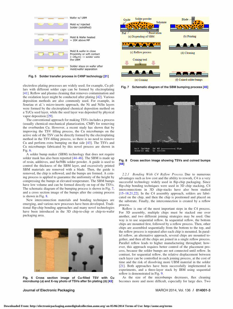
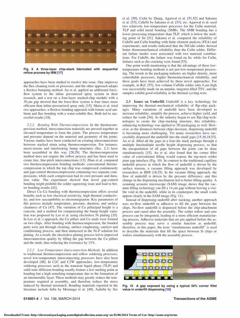
2.1 Bump Structure. Various interconnection types with dif-ferent materials, sizes, and even structures have been reported inrecent years. Common interconnection structures such as micro-bumps and Cu pillars have been used in 3D chip-stacking struc-tures [13–22]. Generally, the trend of the interconnection isbecoming smaller in dimension, finer in pitch, and higher in inter-connection density. Bumps with 10 lm pitch have already beenstudied [14]. Some innovative bump structures invented in recentyears, such as the Ni micro-insert [23–25] and the Cu/Sn inter-locking bump [26,27], have also been applied to 3D interconnec-tions. Figure 3 shows a cross section view of interlocking bumpsfabricated by Jang et al. [28]. Sn bumps (25 lm in diameter and15 lm high) were fabricated on one chip, and the Cu interlockingbumps on the other chip were inserted into the larger Sn bumpsusing the flip-chip bonding process. Planar bumps (70 lm in diam-eter and 10 lm high) directly fabricated on Cu TSV were alsoused in the same paper (Fig. 3). Souriau et al. used micro-insertinterconnection technology in their chip-to-wafer stacking study[29]. In that process, a matrix of micro-inserts made of Ni wasinserted in the soft NiSn material, which was formed on the corre-sponding location on the wafer (or on other dies). An image of themicro-inserts matrix is shown in Fig. 4. These novel structureshave several benefits. First, they meet the trend of miniature in thepackaging industry and enable high-density interconnection, oneof the driving forces of TSV-based 3D integration. Small bumpsize not only reduces the distance between dies but also leavesmore space on the die so that more TSVs can be fabricated. Sec-ond, these structures are compatible with mature flip-chip bondingtechniques for chip-to-chip or chip-to-wafer connections. In addi-tion, the mechanical robustness and electrical performance have
been tested by the inventors [28,30]. Some disadvantages of thesenovel structures have also been pointed out in publications. Forinstance, the micro-insert approach is sensitive to planarity, andnonflatness may increase electrical resistivity [23].
The Cu pillar bump technology has emerged in recent years.This technology enables small pitch size and high interconnectiondensity. Compared with the solder-bump-based interconnection, aCu pillar with a solder cap has many advantages such as higherstandoff, less solder spread out [31,32], etc. Though this technol-ogy was invented not long ago, it has already been used in 3D/2.5D packaging [19,33], and the effect of solder capping materialhas been studied [34]. Direct Cu to Cu bonding using the thermo-compression method, which can connect two Cu pillars (or studs)without using any solder material, has also been researched[35,36].
2.2 Bumping and Assembly Process. Formation of thebumps or pads is an important step in the packaging process. Vari-ous bumping methods have been investigated to make the processmore efficient and reliable.
The controlled collapse chip connection (C4) technology,which was invented by IBM in the 1960s, is a well-establishedinterconnection technology. Different methods of making C4bumps, such as masked evaporation [37], paste screening [38],and photolithographic electroplating [39], have been developedsince its invention. A current C4 bumping technology developedby IBM, the C4-New Process (C4NP), has already been used in3D chip-stacking [21,22,40]. The C4NP process utilizes a glassmold with cavities to transfer solder to the wafer. Molten solder isinjected in the cavities of the mold, and then the mold is alignedbelow the wafer. Then, the wafer and the mold are heated abovethe solder’s melting temperature in a sealed-off manufacturingenvironment so that the solder will wet the underbump metalliza-tion (UBM) and attach to the wafer. The C4NP process flow isschematically depicted in Fig. 5. Compared with other bumpingmethods, this approach combines several advantages, such as thecapability of fabricating fine-pitch bumps in volume production,easy change of solder materials, environmentally friendly manu-facturing (no plating chemical), low cost, etc. [40].
Due to the capability to fabricate tiny bumps, plating is anotherpopular method for bumping and forming UBM. Electrolytic and
Fig. 3 Cross section image showing interlocking Sn/Cu bumps (left) and a Cuplanar bump with TSVs (right) [28]
Fig. 4 Image of fabricated micro-inserts [29]
014001-2 / Vol. 136, MARCH 2014 Transactions of the ASME
Downloaded From: http://electronicpackaging.asmedigitalcollection.asme.org/ on 05/06/2014 Terms of Use: http://asme.org/terms
electroless plating processes are widely used; for example, Cu pil-lars with different solder caps can be formed by electroplating[41]. Reflow and plasma cleaning that removes contamination andthe oxidation layer might be conducted after plating [42]. Variousdeposition methods are also commonly used. For example, inSouriau et al.’s micro-inserts approach, the Ni and NiSn layerswere formed by the electroplated chemical deposition method ona Ti/Cu seed layer, while the seed layer was deposited by physicalvapor deposition [29].
The conventional approach for making TSVs includes a process(usually chemical–mechanical planarization, CMP) for removingthe overburden Cu. However, a recent study has shown that byimproving the TSV filling process, the Cu microbumps on theactive side of the TSV can be directly formed by the electroplatingmethod in the TSV-filling process, so there is no need to removeCu and perform extra bumping on that side [43]. The TSVs andCu microbumps fabricated by this novel process are shown inFig. 6.
A solder bump maker (SBM) technology that does not requiresolder mask has also been reported [44–46]. The SBM is made upof resin, additives, and Sn58Bi solder powder. A guide is used tocontrol the thickness of the SBM layer, and excessively printedSBM materials are removed with a blade. Then, the guide isremoved, the chip is reflowed, and the bumps are formed. A coin-ing process is applied to guarantee the uniformity of the height bycompressing the bumps at elevated temperature. The SBM bumpshave low volume and can be formed directly on top of the TSVs.The schematic diagram of the bumping process is shown in Fig. 7,and a cross section image of the bumps after the coining processis shown in Fig. 8.
New interconnection materials and bonding techniques areemerging, and various new processes have been developed. Tradi-tional flip-chip bonding approaches and many novel technologieshave been introduced in the 3D chip-to-chip or chip-to-waferpackaging area.
2.2.1 Bonding With C4 Reflow Process. Due to numerousadvantages such as low cost and the ability to rework, C4 is a verysuccessful technology widely used in flip-chip packaging. Sinceflip-chip bonding techniques were used in 3D chip stacking, C4interconnections in 3D chip-stacks have also been studied[15–18,21,22]. In the C4 assembly approach, solders are fabri-cated on the chip, and then the chip is positioned and placed onthe substrate. Finally, the interconnection is created by a reflowprocess.
Reflow is one of the most important steps in the C4 process.For 3D assembly, multiple chips must be stacked one overanother, and two different joining strategies may be used. Oneway is to use sequential reflow. In sequential reflow, the bottomchips are mounted first, followed by a reflow process. Then, otherchips are assembled sequentially from the bottom to the top, andthe reflow process is repeated after each chip is mounted. In paral-lel reflow, an alternative approach, several chips are mounted to-gether, and then all the chips are joined in a single reflow process.Parallel reflow leads to higher manufacturing throughput; how-ever, this approach requires better control of the placement pro-cess, because the solder bumps are not connected until reflow. Incontrast, for sequential reflow, the relative displacement betweeneach layer can be controlled in each joining process, at the cost oftime and the risk of dissolving more UBM material in the solder[21]. Both approaches have been successfully implemented inexperiments, and a three-layer stack by IBM using sequentialreflow is demonstrated in Fig. 9.
As the size of the microbumps decreases, flux cleaningbecomes more and more difficult, especially for large dies. Two
Fig. 5 Solder transfer process in C4NP technology [21]
Fig. 6 Cross section image of Cu-filled TSV with Cumicrobump (a) and X-ray photo of TSVs after Sn plating (b) [43]
Fig. 7 Schematic diagram of the SBM bumping process [45]
Fig. 8 Cross section image showing TSVs and coined bumps[44]
Journal of Electronic Packaging MARCH 2014, Vol. 136 / 014001-3
Downloaded From: http://electronicpackaging.asmedigitalcollection.asme.org/ on 05/06/2014 Terms of Use: http://asme.org/terms
approaches have been studied to resolve this issue. One improvesthe flux-cleaning tools or processes, and the other approach adoptsa fluxless bumping method. Au et al. applied an additional force-flow system to the inline pressurized spray system in theirresearch, and a test on a four-layer stacked-chip module with a30 lm gap showed that the force-flow system is four times moreefficient than inline pressurized spray only [15]. Maria et al. triedtwo approaches: a fluxless bonding approach with formic acid am-bient and flux bonding with a water-soluble flux. Both led to suc-cessful results [18].
2.2.2 Bonding With Thermocompression. In the thermocom-pression method, interconnection materials are pressed together atelevated temperature to form the joints. The process temperatureand pressure depend on the material and geometry of the joints.Various studies have been conducted on creating interconnectionsbetween stacked strata using thermocompression. For instance,micro-inserts and interlocking bump structures (Sec. 2.1) havebeen assembled in this way [28,29]. The thermocompressionmethod does not require the reflow process and has been used tocreate tiny, fine-pitch interconnections [13]. Zhan et al. comparedtwo thermocompression bonding methods: conventional thermo-compression in which the top chip was compressed continuouslyand gap-control thermocompression containing two separate com-pressions, while each compression had its own pressure and dura-tion value. The experiment showed that novel gap-controlbonding might prohibit the solder squeezing issue and lead to bet-ter bonding results [42].
Direct Cu–Cu bonding with thermocompression offers severalbenefits such as low electrical resistivity, high thermal conductiv-ity, and low susceptibility to electromigration. Key parameters ofthis process include temperature, pressure, duration, and surfacecleanness of Cu [47]. The variation of Cu pillar/pad height is aconcern, and a method for compensating the bump height varia-tion was proposed by Lee et al. using electroless Ni plating [35].In Lee et al.’s approach, the Cu pillars and Cu studs were formedon two chips. After bonding with thermocompression, the bondedparts were put through cleaning, surface roughening, catalyst andconditioning process, and then immersed in the Ni-P solution forplating. As a result, the electroless plating process led to improvedinterconnection quality by filling the gap between the Cu pillarsand the studs, thus reducing the resistance by 15%.
2.2.3 Low-Temperature Interconnection Methods. In additionto traditional thermocompression and reflow soldering processes,novel low-temperature interconnecting processes have also beendeveloped [48]. In C2C and C2W approaches, low-temperaturesoldering processes such as the transient liquid phase (TLP) andsolid state diffusion bonding usually feature a low melting point atbonding but a high remelting temperature due to the formation ofan intermetallic layer. These methods may greatly reduce the tem-perature required at assembly, and therefore reduce the stressinduced by thermal mismatch. Bonding materials reported in theliterature include InSn by Morinaga et al. [49], AuInSn by Xie
et al. [50], CuSn by Zhang, Agarwal et al. [51,52] and Sakumaet al. [53], CuInNi by Sakuma et al. [53], etc. Agarwal et al. usedtwo relatively low-temperature processes for the CuSn material,TLP and solid metal bonding (SMB). The SMB bonding has alower processing temperature than TLP, which is below the melt-ing point of Sn [51]. Sakuma et al. compared the reliability ofCuInNi and CuSn bonding with finite element analysis (FEA) andexperiments, and results indicated that the NiCuIn solder showedbetter thermomechanical reliability than the CuSn solder. Differ-ent failure modes were associated with two material combina-tions. For CuInNi, the failure was found on In; while for CuSn,failures such as die-cracking were found [53].
One point worth mentioning is that the advantage of these low-temperature bonding methods is not just low-temperature process-ing. The trends in the packaging industry are higher density, morecontrollable processes, higher thermomechanical reliability, andthese goals have been achieved by these novel approaches. Forexample, in Ref. [53], low-volume CuNiIn solder only 6 lm highwas successfully made on an annular, tungsten-filled TSV, and thesamples exhibit good reliability in the thermal cycling tests.
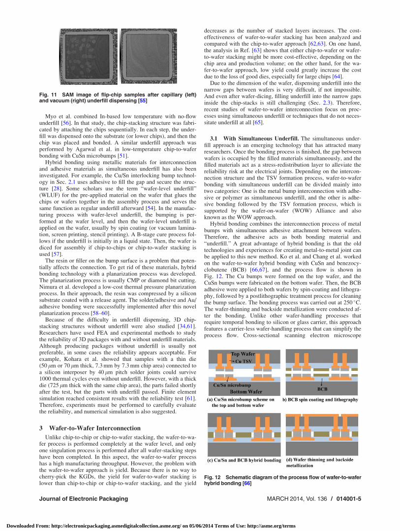
2.3 Issues on Underfill. Underfill is a key technology forimproving the thermal–mechanical reliability of flip-chip pack-ages. Many variations of underfill have been developed toincrease reliability, simplify the process, achieve higher yield, andreduce the voids [54]. As the industry began to use flip-chip tech-nologies to create the chip-stacking structure, this reliability-enhancing technology was applied to 3D packaging as well. How-ever, as the distances between chips decrease, dispensing underfillis becoming more challenging. Yet many researchers have suc-cessfully dispensed the underfill into the small gaps [15,16,18,53].Au et al. filled all the gaps in a four-die stack package through amultiple line/multiple needle height dispensing process, so thatthe encapsulation of all gaps between the joints can be donesimultaneously [15]. Au et al. also found that the corner filletvalue of conventional filling would expose the top-most solderjoint gap interface (Fig. 10). In contrast to the traditional capillaryunderfill process in which the flow of underfill is driven by thesurface tension, a vacuum filling approach was developed byresearchers at IBM [18,55]. In the vacuum filling approach, theflow of underfill is driven by the pressure difference, and thischange in the dispensing mechanism led to better filling quality. Ascanning acoustic microscope (SAM) image shows that the vac-uum filling technology can fill a 14 lm gap without leaving a visi-ble void in the underfill, while in its counterpart, the small voidsappear clearly in the SAM image (Fig. 11).
Instead of dispensing underfill after stacking, another approachuses no-flow underfill or adhesive to fill the gaps between thechips. No-flow underfill is dispensed before the chip-attachmentprocess and cured after the assembly. The solder reflow and cureprocess can be integrated, leading to a more efficient manufactur-ing process. Adhesive materials that are pre-applied before the as-sembly process may serve a similar function as underfill;therefore, in this paper, the term “simultaneous underfill” is usedto describe the materials that fill the space between Si chips orwafers simultaneously with the assembly process.
Fig. 9 A three-layer chip-stack fabricated with sequentialreflow process by IBM [17]
Fig. 10 A gap exposed by using a typical 50% corner filletvalue in underfill dispensing [15]
014001-4 / Vol. 136, MARCH 2014 Transactions of the ASME
Downloaded From: http://electronicpackaging.asmedigitalcollection.asme.org/ on 05/06/2014 Terms of Use: http://asme.org/terms
Myo et al. combined In-based low temperature with no-flowunderfill [56]. In that study, the chip-stacking structure was fabri-cated by attaching the chips sequentially. In each step, the under-fill was dispensed onto the substrate (or lower chips), and then thechip was placed and bonded. A similar underfill approach wasperformed by Agarwal et al. in low-temperature chip-to-waferbonding with CuSn microbumps [51].
Hybrid bonding using metallic materials for interconnectionand adhesive materials as simultaneous underfill has also beeninvestigated. For example, the Cu/Sn interlocking bump technol-ogy in Sec. 2.1 uses adhesive to fill the gap and secure the struc-ture [28]. Some scholars use the term “wafer-level underfill”(WLUF) for the pre-applied material on the wafer that glues thechips or wafers together in the assembly process and serves thesame function as regular underfill afterward [54]. In the manufac-turing process with wafer-level underfill, the bumping is per-formed at the wafer level, and then the wafer-level underfill isapplied on the wafer, usually by spin coating (or vacuum lamina-tion, screen printing, stencil printing). A B-stage cure process fol-lows if the underfill is initially in a liquid state. Then, the wafer isdiced for assembly if chip-to-chips or chip-to-wafer stacking isused [57].
The resin or filler on the bump surface is a problem that poten-tially affects the connection. To get rid of these materials, hybridbonding technology with a planarization process was developed.The planarization process is usually CMP or diamond bit cutting.Nimura et al. developed a low-cost thermal pressure planarizationprocess. In their approach, the resin was compressed by a siliconsubstrate coated with a release agent. The solder/adhesive and Au/adhesive bonding were successfully implemented after this novelplanarization process [58–60].
Because of the difficulty in underfill dispensing, 3D chip-stacking structures without underfill were also studied [34,61].Researchers have used FEA and experimental methods to studythe reliability of 3D packages with and without underfill materials.Although producing packages without underfill is usually notpreferable, in some cases the reliability appears acceptable. Forexample, Kohara et al. showed that samples with a thin die(50 lm or 70 lm thick, 7.3 mm by 7.3 mm chip area) connected toa silicon interposer by 40 lm pitch solder joints could survive1000 thermal cycles even without underfill. However, with a thickdie (725 lm thick with the same chip area), the parts failed shortlyafter the test, but the parts with underfill passed. Finite elementsimulation reached consistent results with the reliability test [61].Therefore, experiments must be performed to carefully evaluatethe reliability, and numerical simulation is also suggested.
3 Wafer-to-Wafer Interconnection
Unlike chip-to-chip or chip-to-wafer stacking, the wafer-to-wa-fer process is performed completely at the wafer level, and onlyone singulation process is performed after all wafer-stacking stepshave been completed. In this aspect, the wafer-to-wafer processhas a high manufacturing throughput. However, the problem withthe wafer-to-wafer approach is yield. Because there is no way tocherry-pick the KGDs, the yield for wafer-to-wafer stacking islower than chip-to-chip or chip-to-wafer stacking, and the yield
decreases as the number of stacked layers increases. The cost-effectiveness of wafer-to-wafer stacking has been analyzed andcompared with the chip-to-wafer approach [62,63]. On one hand,the analysis in Ref. [63] shows that either chip-to-wafer or wafer-to-wafer stacking might be more cost-effective, depending on thechip area and production volume; on the other hand, for the wa-fer-to-wafer approach, low yield could greatly increase the costdue to the loss of good dies, especially for large chips [64].
Due to the dimension of the wafer, dispensing underfill into thenarrow gaps between wafers is very difficult, if not impossible.And even after wafer-dicing, filling underfill into the narrow gapsinside the chip-stacks is still challenging (Sec. 2.3). Therefore,recent studies of wafer-to-wafer interconnection focus on proc-esses using simultaneous underfill or techniques that do not neces-sitate underfill at all [65].
3.1 With Simultaneous Underfill. The simultaneous under-fill approach is an emerging technology that has attracted manyresearchers. Once the bonding process is finished, the gap betweenwafers is occupied by the filled materials simultaneously, and thefilled materials act as a stress-redistribution layer to alleviate thereliability risk at the electrical joints. Depending on the intercon-nection structure and the TSV formation process, wafer-to-waferbonding with simultaneous underfill can be divided mainly intotwo categories: One is the metal bump interconnection with adhe-sive or polymer as simultaneous underfill, and the other is adhe-sive bonding followed by the TSV formation process, which issupported by the wafer-on-wafer (WOW) Alliance and alsoknown as the WOW approach.
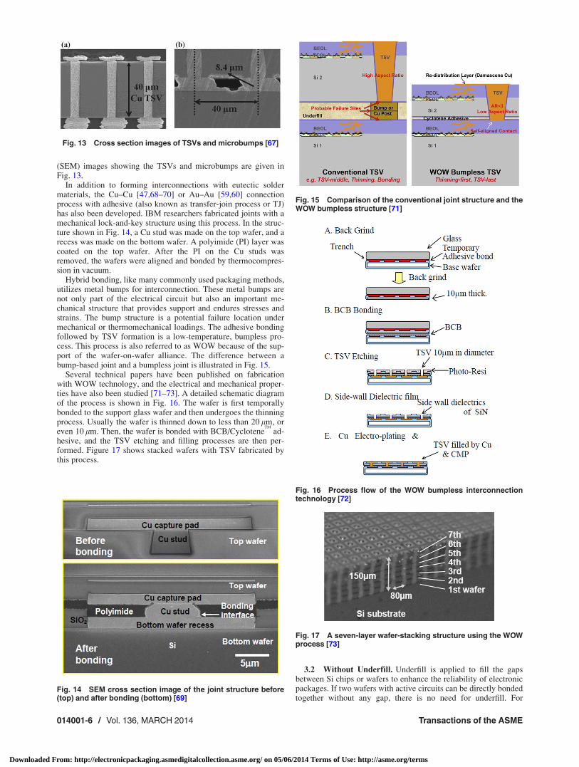
Hybrid bonding combines the interconnection process of metalbumps with simultaneous adhesive attachment between wafers.Therefore, the adhesive acts as both bonding material and“underfill.” A great advantage of hybrid bonding is that the oldtechnologies and experiences for creating metal-to-metal joint canbe applied to this new method. Ko et al. and Chang et al. workedon the wafer-to-wafer hybrid bonding with CuSn and benezocy-clobutene (BCB) [66,67], and the process flow is shown inFig. 12. The Cu bumps were formed on the top wafer, and theCuSn bumps were fabricated on the bottom wafer. Then, the BCBadhesive were applied to both wafers by spin-coating and lithogra-phy, followed by a postlithographic treatment process for cleaningthe bump surface. The bonding process was carried out at 250 �C.The wafer-thinning and backside metallization were conducted af-ter the bonding. Unlike other wafer-handling processes thatrequire temporal bonding to silicon or glass carrier, this approachfeatures a carrier-less wafer-handling process that can simplify theprocess flow. Cross-sectional scanning electron microscope
Fig. 11 SAM image of flip-chip samples after capillary (left)and vacuum (right) underfill dispensing [55]
Fig. 12 Schematic diagram of the process flow of wafer-to-waferhybrid bonding [66]
Journal of Electronic Packaging MARCH 2014, Vol. 136 / 014001-5
Downloaded From: http://electronicpackaging.asmedigitalcollection.asme.org/ on 05/06/2014 Terms of Use: http://asme.org/terms
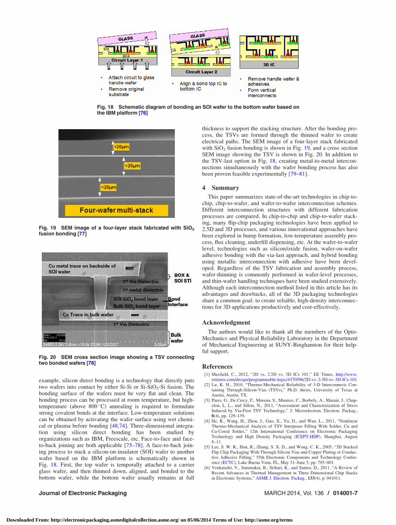
(SEM) images showing the TSVs and microbumps are given inFig. 13.
In addition to forming interconnections with eutectic soldermaterials, the Cu–Cu [47,68–70] or Au–Au [59,60] connectionprocess with adhesive (also known as transfer-join process or TJ)has also been developed. IBM researchers fabricated joints with amechanical lock-and-key structure using this process. In the struc-ture shown in Fig. 14, a Cu stud was made on the top wafer, and arecess was made on the bottom wafer. A polyimide (PI) layer wascoated on the top wafer. After the PI on the Cu studs wasremoved, the wafers were aligned and bonded by thermocompres-sion in vacuum.
Hybrid bonding, like many commonly used packaging methods,utilizes metal bumps for interconnection. These metal bumps arenot only part of the electrical circuit but also an important me-chanical structure that provides support and endures stresses andstrains. The bump structure is a potential failure location undermechanical or thermomechanical loadings. The adhesive bondingfollowed by TSV formation is a low-temperature, bumpless pro-cess. This process is also referred to as WOW because of the sup-port of the wafer-on-wafer alliance. The difference between abump-based joint and a bumpless joint is illustrated in Fig. 15.
Several technical papers have been published on fabricationwith WOW technology, and the electrical and mechanical proper-ties have also been studied [71–73]. A detailed schematic diagramof the process is shown in Fig. 16. The wafer is first temporallybonded to the support glass wafer and then undergoes the thinningprocess. Usually the wafer is thinned down to less than 20 lm, oreven 10 lm. Then, the wafer is bonded with BCB/Cyclotene
TM
ad-hesive, and the TSV etching and filling processes are then per-formed. Figure 17 shows stacked wafers with TSV fabricated bythis process.
3.2 Without Underfill. Underfill is applied to fill the gapsbetween Si chips or wafers to enhance the reliability of electronicpackages. If two wafers with active circuits can be directly bondedtogether without any gap, there is no need for underfill. For
Fig. 13 Cross section images of TSVs and microbumps [67]
Fig. 14 SEM cross section image of the joint structure before(top) and after bonding (bottom) [69]
Fig. 15 Comparison of the conventional joint structure and theWOW bumpless structure [71]
Fig. 16 Process flow of the WOW bumpless interconnectiontechnology [72]
Fig. 17 A seven-layer wafer-stacking structure using the WOWprocess [73]
014001-6 / Vol. 136, MARCH 2014 Transactions of the ASME
Downloaded From: http://electronicpackaging.asmedigitalcollection.asme.org/ on 05/06/2014 Terms of Use: http://asme.org/terms
example, silicon direct bonding is a technology that directly putstwo wafers into contact by either Si-Si or Si-SiO2-Si fusion. Thebonding surface of the wafers must be very flat and clean. Thebonding process can be processed at room temperature, but high-temperature (above 800 �C) annealing is required to formulatestrong covalent bonds at the interface. Low-temperature solutionscan be obtained by activating the wafer surface using wet chemi-cal or plasma before bonding [48,74]. Three-dimensional integra-tion using silicon direct bonding has been studied byorganizations such as IBM, Freescale, etc. Face-to-face and face-to-back joining are both applicable [75–78]. A face-to-back join-ing process to stack a silicon-on-insulator (SOI) wafer to anotherwafer based on the IBM platform is schematically shown inFig. 18. First, the top wafer is temporally attached to a carrierglass wafer, and then thinned down, aligned, and bonded to thebottom wafer, while the bottom wafer usually remains at full
thickness to support the stacking structure. After the bonding pro-cess, the TSVs are formed through the thinned wafer to createelectrical paths. The SEM image of a four-layer stack fabricatedwith SiO2 fusion bonding is shown in Fig. 19, and a cross sectionSEM image showing the TSV is shown in Fig. 20. In addition tothe TSV-last option in Fig. 18, creating metal-to-metal intercon-nections simultaneously with the wafer bonding process has alsobeen proven feasible experimentally [79–81].
4 Summary
This paper summarizes state-of-the-art technologies in chip-to-chip, chip-to-wafer, and wafer-to-wafer interconnection schemes.Different interconnection structures with different fabricationprocesses are compared. In chip-to-chip and chip-to-wafer stack-ing, many flip-chip packaging technologies have been applied to2.5D and 3D processes, and various innovational approaches havebeen explored in bump formation, low-temperature assembly pro-cess, flux cleaning, underfill dispensing, etc. At the wafer-to-waferlevel, technologies such as silicon/oxide fusion, wafer-on-waferadhesive bonding with the via-last approach, and hybrid bondingusing metallic interconnection with adhesive have been devel-oped. Regardless of the TSV fabrication and assembly process,wafer-thinning is commonly performed in wafer-level processes,and thin-wafer handling techniques have been studied extensively.Although each interconnection method listed in this article has itsadvantages and drawbacks, all of the 3D packaging technologiesshare a common goal: to create reliable, high-density interconnec-tions for 3D applications productively and cost-effectively.
Acknowledgment
The authors would like to thank all the members of the Opto-Mechanics and Physical Reliability Laboratory in the Departmentof Mechanical Engineering at SUNY-Binghamton for their help-ful support.
References[1] Maxfield, C., 2012, “2D vs. 2.5D vs. 3D ICs 101,” EE Times, http://www.
eetimes.com/design/programmable-logic/4370596/2D-vs–2-5D-vs–3D-ICs-101[2] Lu, K. H., 2010, “Thermo-Mechanical Reliability of 3-D Interconnects Con-
taining Through-Silicon-Vias (TSVs),” Ph.D. thesis, University of Texas atAustin, Austin, TX.
[3] Pares, G., De Crecy, F., Moreau, S., Maurice, C., Borbely, A., Mazuir, J., Chap-elon, L. L., and Sillon, N., 2011, “Assessment and Characterization of StressInduced by Via-First TSV Technology,” J. Microelectron. Electron. Packag.,8(4), pp. 129–139.
[4] He, R., Wang, H., Zhou, J., Guo, X., Yu, D., and Wan, L., 2011, “NonlinearThermo-Mechanical Analysis of TSV Interposer Filling With Solder, Cu andCu-Cored Solder,” 12th International Conference on Electronic PackagingTechnology and High Density Packaging (ICEPT-HDP), Shanghai, August8–11.
[5] Lee, S. W. R., Hon, R., Zhang, S. X. D., and Wong, C. K., 2005, “3D StackedFlip Chip Packaging With Through Silicon Vias and Copper Plating or Conduc-tive Adhesive Filling,” 55th Electronic Components and Technology Confer-ence (ECTC), Lake Buena Vista, FL, May 31–June 5, pp. 795–801.
[6] Venkatadri, V., Sammakia, B., Srihari, K., and Santos, D., 2011, “A Review ofRecent Advances in Thermal Management in Three Dimensional Chip Stacksin Electronic Systems,” ASME J. Electron. Packag., 133(4), p. 041011.
Fig. 18 Schematic diagram of bonding an SOI wafer to the bottom wafer based onthe IBM platform [76]
Fig. 19 SEM image of a four-layer stack fabricated with SiO2
fusion bonding [77]
Fig. 20 SEM cross section image showing a TSV connectingtwo bonded wafers [78]
Journal of Electronic Packaging MARCH 2014, Vol. 136 / 014001-7
Downloaded From: http://electronicpackaging.asmedigitalcollection.asme.org/ on 05/06/2014 Terms of Use: http://asme.org/terms

[7] Onkaraiah, S., and Chuan Seng, T., 2010, “Mitigating Heat Dissipation andThermo-Mechanical Stress Challenges in 3-D IC Using Thermal Through Sili-con Via (TTSV),” 60th Electronic Components and Technology Conference(ECTC), Las Vegas, NV, June 1–4, pp. 411–416.
[8] Santarini, M., 2011, “Stacked & Loaded: Xilinx SSI, 28-Gbps I/O Yield Amaz-ing FPGAs,” Xcell J., 74(1), pp. 8–13.
[9] Tu, K. N., Hsiao, H.-Y., and Chen, C., 2012, “Transition From Flip Chip SolderJoint to 3D IC Microbump: Its Effect on Microstructure Anisotropy,” Micro-electron. Reliab., 53(1), pp. 2–6.
[10] Tu, K. N., 2011, “Reliability Challenges in 3D IC Packaging Technology,”Microelectron. Reliab., 51(3), pp. 517–523.
[11] Dunne, R., Takahashi, Y., Mawatari, K., Matsuura, M., Bonifield, T., Stein-mann, P., and Stepniak, D., 2012, “Development of a Stacked WCSP PackagePlatform Using TSV (Through Silicon Via) Technology,” IEEE 62nd Elec-tronic Components and Technology Conference (ECTC), San Diego, CA, May29–June 1, pp. 1062–1067.
[12] Chen, Q., Zhang, D., Xu, Z., Beece, A., Patti, R., Tan, Z., Wang, Z., Liu, L.,and Lu, J.-Q., 2012, “A Novel Chip-to-Wafer (C2W) Three-Dimensional (3D)Integration Approach Using a Template for Precise Alignment,” Microelectron.Eng., 92, pp. 15–18.
[13] Yu, A., Lau, J. H., Ho, S. W., Kumar, A., Hnin, W. Y., Yu, D.-Q., Jong, M. C.,Kripesh, V., Pinjala, D., and Kwong, D.-L., 2009, “Study of 15lm Pitch SolderMicrobumps for 3D IC Integration,” 59th Electronic Components and Technol-ogy Conference (ECTC), San Diego, CA, May 26–29, pp. 6–10.
[14] Lee, C.-K., Zhan, C.-J., Lau, J. H., Huang, Y.-J., Fu, H.-C., Huang, J.-H., Hsiao,Z.-C., Chen, S.-W., Huang, S.-Y., Fan, C.-W., Lin, Y.-M., Kao, K.-S., Ko,C.-T., Chen, T.-H., Lo, R., and Kao, M. J., 2012, “Wafer Bumping, Assembly,and Reliability Assessment of l bumps With 5lm Pads on 10 lm Pitch for 3DIC Integration,” 62nd Electronic Components and Technology Conference(ECTC), San Diego, CA, May 29–June 1, pp. 636–640.
[15] Au, K. Y., Beleran, J. D., Yang, Y. B., Zhang, Y. F., Kriangsak, S. L., Wilson, P. L. O.,Drake, Y. S. K., Toh, C. H., and Surasit, C., 2011, “Thru Silicon Via Stacking &Numerical Characterization for Multi-Die Interconnections Using Full Array &Very Fine Pitch Micro C4 Bumps,” 61st Electronic Components and TechnologyConference (ECTC), Lake Buena Vista, FL, May 31–June 3, pp. 296–303.
[16] Au, K. Y., Kriangsak, S. L., Zhang, X. R., Zhu, W. H., and Toh, C. H., 2010,“3D Chip Stacking & Reliability Using TSV-Micro C4 Solder Inter-connection,” 60th Electronic Components and Technology Conference(ECTC), Las Vegas, NV, June 1–4, pp. 1376–1384.
[17] Dang, B., Wright, S. L., Andry, P. S., Sprogis, E. J., Tsang, C. K., Interrante,M. J., Webb, B. C., Polastre, R. J., Horton, R. R., Patel, C. S., Sharma, A.,Zheng, J., Sakuma, K., and Knickerbocker, J. U., 2008, “3D Chip StackingWith C4 Technology,” IBM J. Res. Dev., 52(6), pp. 599–609.
[18] Maria, J., Dang, B., Wright, S. L., Tsang, C. K., Andry, P., Polastre, R., Liu, Y.,Wiggins, L., and Knickerbocker, J. U., 2011, “3D Chip Stacking With 50 lmPitch Lead-Free Micro-C4 Interconnections,” 61st Electronic Components andTechnology Conference (ECTC), Lake Buena Vista, FL, May 31–June 3, pp.268–273.
[19] Patterson, D. S., 2012, “2.5D/3D Packaging Enablement Through Copper PillarTechnology,” Chip Scale Review, 16(3), pp. 20–26.
[20] Farooq, M. G., Graves-Abe, T. L., Landers, W. F., Kothandaraman, C., Him-mel, B. A., Andry, P. S., Tsang, C. K., Sprogis, E., Volant, R. P., Petrarca, K.S., Winstel, K. R., Safran, J. M., Sullivan, T. D., Chen, F., Shapiro, M. J., Han-non, R., Liptak, R., Berger, D., and Iyer, S. S., 2011, “3D Copper TSV Integra-tion, Testing and Reliability,” 2011 IEEE International Electron DevicesMeeting (IEDM), Washington, DC, December 5–7, pp. 7.1.1–7.1.4.
[21] Busby, J., Dang, B., Gruber, P., Hawken, D., Shah, J., Weisman, R., Perfecto,E., Ruhmer, K., and Buchwalter, S., 2008, “C4NP Lead Free Solder Bumpingand 3D Micro Bumping,” IEEE/SEMI Advanced Semiconductor Manufactur-ing Conference (ASMC 2008), Cambridge, MA, May 5–7, pp. 333–339.
[22] Shih, D. Y., Dang, B., Gruber, P., Lu, M., Kang, S., Buchwalter, S., Knicker-bocker, J., Perfecto, E., Garant, J., Knickerbocker, S., Semkow, K., Sundlof, B.,Busby, J., Weisman, R., Ruhmer, K., and Hughlett, E., 2008, “C4NP for Pb-Free Solder Wafer Bumping and 3D Fine-Pitch Applications,” InternationalConference on Electronic Packaging Technology and High Density Packaging(ICEPT-HDP), Shanghai, July 28–31.
[23] Mathewson, A., Brun, J., Ponthenier, G., Franiatte, R., Nowodzinski, A., Sillon,N., Poupon, G., Deputot, F., and Dubois-Bonvalot, B., 2007, “Detailed Charac-terisation of Ni Microinsert Technology For Flip Chip Die on WaferAttachment,” 57th Electronic Components and Technology Conference(ECTC), Reno, NV, May 29-June 1, pp. 616–621.
[24] Mathewson, A., Brun, J., Puget, C., Franiatte, R., Sillon, N., Depoutot, F., andDubois-Bonvalot, B., 2006, “Microstructured Interconnections for High Secu-rity Systems,” 1st Electronics Systemintegration Technology Conference, Dres-den, Germany, September 5–7, pp. 126–132.
[25] Poupon, G., Sillon, N., Henry, D., Gillot, C., Mathewson, A., Di Cioccio, L.,Charlet, B., Leduc, P., Vinet, M., and Batude, P., 2009, “System on Wafer: ANew Silicon Concept in SiP,” Proc. IEEE, 97(1), pp. 60–69.
[26] Park, S.-H., Lee, K.-Y., Won, H.-J., Oh, T.-S., and Kim, Y.-H., 2007, “FlipChip Process Using Mushroom Bumps and Interlocking Bumps,” 40th Interna-tional Symposium on Microelectronics (IMAPS 2007), San Jose, CA, Novem-ber 11–15, pp. 723–727.
[27] Oh, T. S., Lee, K.-Y., and Won, H.-J., 2009, “Flip-Chip Process UsingInterlocking-Bump Joints,” IEEE Trans. Compon. Packag. Technol., 32(4), pp.909–914.
[28] Jang, D. M., Ryu, C., Lee, K. Y., Cho, B. H., Kim, J., Oh, T. S., Lee, W. J., andYu, J., 2007, “Development and Evaluation of 3-D SiP With Vertically Inter-
connected Through Silicon Vias (TSV),” 57th Electronic Components andTechnology Conference (ECTC), Reno, NV, May 29–June 1, pp. 847–852.
[29] Souriau, J. C., Castagne, L., Liotard, J., Inal, K., Mazuir, J., Le Texier, F., Fres-quet, G., Varvara, M., Launay, N., Dubois, B., and Malia, T., 2012, “3D Multi-Stacking of Thin Dies Based on TSV and Micro-Inserts Interconnections,”62nd Electronic Components and Technology Conference (ECTC), San Diego,CA, May 29–June 1, pp. 1047–1053.
[30] Nowodzinski, A., Boutry, H., Franiatte, R., Mandrillon, V., Anciant, R., Verrun,S., and Simon, G., 2012, “Reliability Tests on Micro-Insert Die Bonding Tech-nology,” International Semiconductor Conference Dresden-Grenoble (ISCDG),Grenoble, France, September 24–26, pp. 83–87.
[31] Ebersberger, B., and Lee, C., 2008, “Cu Pillar Bumps as a Lead-Free Drop-InReplacement for Solder-Bumped, Flip-Chip Interconnects,” 58th ElectronicComponents and Technology Conference (ECTC), Lake Buena Vista, FL, May27–30, pp. 59–66.
[32] Lee, C. H., 2009, “Interconnection With Copper Pillar Bumps: Process andApplications,” IEEE International Interconnect Technology Conference (IITC2009), Sapporo, Japan, June 1–3, pp. 214–216.
[33] Chang, J. Y., Cheng, R. S., Kao, K. S., Chang, T. C., and Chuang, T. H., 2012,“Reliable Microjoints Formed by Solid–Liquid Interdiffusion (SLID) BondingWithin a Chip-Stacking Architecture,” IEEE Trans. Compon., Packag. Manuf.Technol., 2(6), pp. 979–984.
[34] Sa, Y.-K., Yoo, S., Shin, Y.-S., Han, M.-K., and Lee, C.-W., 2010, “Joint Prop-erties of Solder Capped Copper Pillars for 3D Packaging,” 60th ElectronicComponents and Technology Conference (ECTC), Las Vegas, NV, June 1–4,pp. 2019–2024.
[35] Lee, J., Fernandez, D. M., Paing, M., Yeo, Y. C., and Gao, S., 2012,“Electroless Ni Plating to Compensate for Bump Height Variation in Cu-Cu3-D Packaging,” IEEE Trans. Compon., Packag. Manuf. Technol., 2(6), pp.964–970.
[36] Tang, Y.-S., Chang, Y.-J., and Chen, K.-N., 2012, “Wafer-Level Cu–Cu Bond-ing Technology,” Microelectron. Reliab., 52(2), pp. 312–320.
[37] Miller, L. F., 1969, “Controlled Collapse Reflow Chip Joining,” IBM J. Res.Dev., 13, pp. 239–250.
[38] Kripesh, V., Wong Wai, K., and Iyer, M., 2003, “Ultra-Fine Pitch Pb-Free &Eutectic Solder Bumping With Fine Particle Size Solder Paste for Nano Pack-aging,” 5th Electronics Packaging Technology Conference (EPTC 2003), Sin-gapore, December 10–12, pp. 732–737.
[39] Gan, H., Wright, S. L., Polastre, R., Buchwalter, L. P., Horton, R., Andry, P. S.,Patel, C., Tsang, C., Knickerbocker, J., Sprogis, E., Pavlova, A., Kang, S. K.,and Lee, K. W., 2006, “Pb-Free Microjoints (50 lm Pitch) for the Next Genera-tion Microsystems: the Fabrication, Assembly and Characterization,” 56th Elec-tronic Components and Technology Conference (ECTC), San Diego, CA, May30–June 2.
[40] Dang, B., Shih, D.-Y., Buchwalter, S., Tsang, C., Patel, C., Knickerbocker, J.,Gruber, P., Knickerbocker, S., Garant, J., Semkow, K., Ruhmer, K., and Hugh-lett, E., 2008, “50 lm Pitch Pb-Free Micro-Bumps by C4NP Technology,” 58thElectronic Components and Technology Conference (ECTC), Lake BuenaVista, FL, May 27–30, pp. 1505–1510.
[41] Yin, W., Yu, D., Dai, F., Song, C., Bo, Z., Wan, L., Yu, H., and Sun, J., 2012,“Development of Micro-Alloying Method for Cu Pillar Solder Bump by SolidLiquid Interaction,” 62nd Electronic Components and Technology Conference(ECTC), San Diego, CA, May 29–June 1, pp. 1709–1714.
[42] Zhan, C.-J., Chuang, C.-C., Juang, J.-Y., Lu, S.-T., and Chang, T.-C., 2010,“Assembly and Reliability Characterization of 3D Chip Stacking With 30 lm PitchLead-Free Solder Micro Bump Interconnection,” 60th Electronic Components andTechnology Conference (ECTC), Las Vegas, NV, June 1–4, pp. 1043–1049.
[43] Ma, S., Sun, X., Zhu, Y., Zhu, Z., Cui, Q., Chen, M., Xiao, Y., Chen, J., Miao,M., Lu, W., and Jin, Y., 2012, “Design and Process Development of a StackedSRAM Memory Chip Module With TSV Interconnection,” 62nd ElectronicComponents and Technology Conference (ECTC), San Diego, CA, May29–June 1, pp. 1925–1929.
[44] Bae, H.-C., Choi, K.-S., Eom, Y.-S., Lim, B.-O., Sung, K.-J., Jung, S., Kim, B.-G., Kang, I.-S., and Moon, J.-T., 2010, “3D SiP Module Using TSV and NovelSolder Bump Maker,” 60th Electronic Components and Technology Confer-ence (ECTC), Las Vegas, NV, June 1–4, pp. 1637–1641.
[45] Sung, K.-J., Choi, K.-S., Bae, H.-C., Kwon, Y.-H., and Eom, Y.-S., 2012,“Novel Bumping and Underfill Technologies for 3D IC Integration,” ETRI J.,34(5), pp. 706–712.
[46] Sung, K.-J., Choi, K.-S., Lim, B.-O., Bae, H.-C., Choo, S.-W., Moon, J.-T.,Kwon, Y. H., Nam, E. S., and Eom, Y.-S., 2010, “Solder Bump Maker WithCoining Process on TSV Chips for 3D Packages,” 11th International Confer-ence on Electronic Packaging Technology and High Density Packaging(ICEPT-HDP), Xi’an, China, August 16–19, pp. 185–189.
[47] Xie, Y., Cong, J. J., and Sapatnekar, S., 2010, 3D Process Technology Consid-erations, Three-Dimensional Integrated Circuit Design: EDA, Design andMicroarchitectures, Springer, New York.
[48] Ko, C.-T., and Chen, K.-N., 2012, “Low Temperature Bonding Technology for3D Integration,” Microelectron. Reliab., 52(2), pp. 302–311.
[49] Morinaga, E., Oka, Y., Nishimori, H., Miyagawa, H., Satoh, R., Iwata, Y., andKanezaki, R., 2012, “Study of Low Temperature and High Heat-Resistant Flux-less Bonding Via Nanoscale Thin Film Control Toward Wafer-Level MultipleChip Stacking for 3D LSI,” 62nd Electronic Components and Technology Con-ference (ECTC), San Diego, CA, May 29–June 1, pp. 14–19.
[50] Xie, L., Choi, W. K., Premachandran, C. S., Selvanayagam, C. S., Bai, K. W.,Zeng, Y. Z., Ong, S. C., Liao, E., Khairyanto, A., Sekhar, V. N., and Thew, S.,2011, “Design, Simulation and Process Optimization of AuInSn Low Temperature
014001-8 / Vol. 136, MARCH 2014 Transactions of the ASME
Downloaded From: http://electronicpackaging.asmedigitalcollection.asme.org/ on 05/06/2014 Terms of Use: http://asme.org/terms
TLP Bonding for 3D IC Stacking,” 61st Electronic Components and TechnologyConference (ECTC), Lake Buena Vista, FL, May 31–June 3, pp. 279–284.
[51] Agarwal, R., Zhang, W., Limaye, P., Labie, R., Dimcic, B., Phommahaxay, A.,and Soussan, P., 2010, “Cu/Sn Microbumps Interconnect for 3D TSV ChipStacking,” 60th Electronic Components and Technology Conference (ECTC),Las Vegas, NV, June 1–4, pp. 858–863.
[52] Zhang, W., Limaye, P., Civale, Y., Labie, R., and Soussan, P., 2010, “Fine PitchCu/Sn Solid State Diffusion Bonding for Making High Yield Bump Intercon-nections and Its Application in 3D Integration,” 3rd Electronic System-Integration Technology Conference (ESTC), Berlin, September 13–16.
[53] Sakuma, K., Sueoka, K., Kohara, S., Matsumoto, K., Noma, H., Aoki, T.,Oyama, Y., Nishiwaki, H., Andry, P. S., Tsang, C. K., Knickerbocker, J. U.,and Orii, Y., 2010, “IMC Bonding for 3D Interconnection,” 60th ElectronicComponents and Technology Conference (ECTC), Las Vegas, NV, June 1–4,pp. 864–871.
[54] Zhang, Z., and Wong, C. P., 2004, “Recent Advances in Flip-Chip Underfill:Materials, Process, and Reliability,” IEEE Trans. Adv. Packag., 27(3), pp.515–524.
[55] Sakuma, K., Kohara, S., Sueoka, K., Orii, Y., Kawakami, M., Asai, K., Hir-ayama, Y., and Knickerbocker, J. U., 2011, “Development of Vacuum UnderfillTechnology for a 3D Chip Stack,” J. Micromechan. Microeng., 21(3), p.035024.
[56] Myo, P., Chong, S. C., Xie, L., Ho, S. W., Toh, W. H. S., and Chai, T. C., 2010,“3D Stacking by Hybrid Bonding With Low Temperature Solder,” 12th Elec-tronics Packaging Technology Conference (EPTC), Singapore, December 8–10,pp. 246–250.
[57] Gregory, C., Lueck, M., Huffman, A., Lannon, J. M., and Temple, D. S., 2012,“High Density Metal-Metal Interconnect Bonding With Pre-Applied FluxingUnderfill,” 62nd Electronic Components and Technology Conference (ECTC),San Diego, CA, May 29–June 1, pp. 20–25.
[58] Nimura, M., Mizuno, J., Sakuma, K., and Shoji, S., 2011, “Solder/AdhesiveBonding Using Simple Planarization Technique for 3D Integration,” 61st Elec-tronic Components and Technology Conference (ECTC), Lake Buena Vista,FL, May 31–June 3, pp. 1147–1152.
[59] Nimura, M., Mizuno, J., Shigetou, A., Sakuma, K., Ogino, H., Enomoto, T., andShoji, S., 2013, “Hybrid Au-Au Bonding Technology Using Planar AdhesiveStructure for 3D Integration,” 63rd Electronic Components and TechnologyConference (ECTC), Las Vegas, NV, May 28–31, pp. 1153–1157.
[60] Nimura, M., Mizuno, J., Shigetou, A., Sakuma, K., Ogino, H., Enomoto, T., andShoji, S., 2013, “Study on Hybrid Au-Underfill Resin Bonding Method WithLock-and-Key Structure for 3-D Integration,” IEEE Trans. Compon., Packag.Manuf. Technol., 3(4), pp. 558–565.
[61] Kohara, S., Horibe, A., Sueoka, K., Matsumoto, K., Yamada, F., Orii, Y.,Sakuma, K., Kinoshita, T., and Kawakami, T., 2012, “Thermal Stress Analysis ofDie Stacks With Fine-Pitch IMC Interconnections for 3D Integration,” IEEEInternational 3D Systems Integration Conference (3DIC), Osaka, Japan, January31–February 2.
[62] Dong, X., and Xie, Y., 2009, “System-Level Cost Analysis and Design Explora-tion for Three-Dimensional Integrated Circuits (3D ICs),” 14th Asia and SouthPacific Design Automation Conference (ASP-DAC 2009), Yokohama, Japan,January 19–22, pp. 234–241.
[63] Chen, Y., Niu, D., Xie, Y., and Chakrabarty, K., 2010, “Cost-Effective Integra-tion of Three-Dimensional (3D) ICs Emphasizing Testing Cost Analysis,”IEEE/ACM International Conference on Computer-Aided Design (ICCAD),San Jose, CA, November 7–11, pp. 471–476.
[64] Lecarpentier, G., Agarwal, R., Wenqizhang, Limaye, P., Labie, R., Phomma-haxay, A., and Soussan, P., 2010, “Die-to-Wafer Bonding of Thin Dies Using a2-Step Approach; High Accuracy Placement, Then Gang Bonding,” 6th Interna-tional Conference and Exhibit on Device Packaging, Scottsdale/Fountain Hills,AZ, March 7–11.
[65] Ko, C.-T., and Chen, K.-N., 2010, “Wafer Level Bonding/Stacking Technologyfor 3D Integration,” Microelectron. Reliab., 50(4), pp. 481–488.
[66] Ko, C.-T., Hsiao, Z.-C., Chang, Y.-J., Chen, P.-S., Hwang, Y.-J., Fu, H.-C.,Huang, J.-H., Chiang, C.-W., Sheu, S.-S., Chen, Y.-H., Lo, W.-C., and Chen,K.-N., 2012, “A Wafer-Level Three-Dimensional Integration Scheme With CuTSVs Based on Microbump/Adhesive Hybrid Bonding for Three-DimensionalMemory Application,” IEEE Trans. Device Mater. Reliab., 12(2), pp. 209–216.
[67] Chang, Y. J., Ko, C. T., Hsiao, Z. C., Yu, T. H., Chen, Y. H., Lo, W. C., andChen, K. N., 2012, “Electrical Characterization and Reliability Investigationsof Cu TSVs With Wafer-Level Cu/Sn-BCB Hybrid Bonding,” InternationalSymposium on VLSI Technology, Systems, and Applications (VLSI-TSA),Hsinchu, Taiwan, April 23–25.
[68] Huyghebaert, C., Van Olmen, J., Civale, Y., Phommahaxay, A., Jourdain, A.,Sood, S., Farrens, S., and Soussan, P., 2010, “Cu to Cu Interconnect Using 3D-TSV and Wafer to Wafer Thermocompression Bonding,” 2010 InternationalInterconnect Technology Conference (IITC), Burlingame, CA, June 6–9.
[69] Liu, F., Yu, R. R., Young, A. M., Doyle, J. P., Wang, X., Shi, L., Chen, K. N.,Li, X., Dipaola, D. A., Brown, D., Ryan, C. T., Hagan, J. A., Wong, K. H., Lu,M., Gu, X., Klymko, N. R., Perfecto, E. D., Merryman, A. G., Kelly, K. A.,Purushothaman, S., Koester, S. J., Wisnieff, R., and Haensch, W., 2008, “A300-mm Wafer-Level Three-Dimensional Integration Scheme Using TungstenThrough-Silicon Via and Hybrid Cu-Adhesive Bonding,” IEEE InternationalElectron Devices Meeting (IEDM 2008), San Francisco, CA, December 15-17.
[70] Swinnen, B., Ruythooren, W., De Moor, P., Bogaerts, L., Carbonell, L., DeMunck, K., Eyckens, B., Stoukatch, S., Sabuncuoglu Tezcan, D., Tokei, Z.,Vaes, J., Van Aelst, J., and Beyne, E., 2006, “3D Integration by Cu-CuThermo-Compression Bonding of Extremely Thinned Bulk-Si Die Containing10 lm Pitch Through-Si Vias,” International Electron Devices Meeting (IEDM’06), San Francisco, CA, December 11–13.
[71] Diehl, D., Kitada, H., Maeda, N., Fujimoto, K., Ramaswami, S., Sirajuddin, K.,Yalamanchili, R., Eaton, B., Rajagopalan, N., Ding, R., Patel, S., Cao, Z.,Gage, M., Wang, Y., Tu, W., Kim, S. W., Kulzer, R., Drucker, I., Erickson, D.,Ritzdorf, T., Nakamura, T., and Ohba, T., 2012, “Formation of TSV for theStacking of Advanced Logic Devices Utilizing Bumpless Wafer-on-WaferTechnology,” Microelectron. Eng., 92, pp. 3–8.
[72] Fujimoto, K., Maeda, N., Kitada, H., Kim, Y. S., Kodama, S., Nakamura, T.,Suzuki, K., and Ohba, T., 2012, “Development of Cost-Effective Wafer LevelProcess for 3D-Integration With Bump-Less TSV Interconnects,” 62nd Elec-tronic Components and Technology Conference (ECTC), San Diego, CA, May29–June 1, pp. 537–540.
[73] Kitada, H., Maeda, N., Fujimoto, K., Suzuki, K., Kawai, A., Arai, K., Suzuki,T., Nakamura, T., and Ohba, T., 2009, “Stress Sensitivity Analysis on TSVStructure of Wafer-on-a-Wafer (WOW) by the Finite Element Method (FEM),”IEEE International Interconnect Technology Conference (IITC), Sapporo,Japan, June 1–3, pp. 107–109.
[74] Ramm, P., Lu, J. J.-Q., and Taklo, M. M. V., 2012, Handbook of Wafer Bond-ing, Wiley-VCH, Weinheim, Germany.
[75] Chatterjee, R., Fayolle, M., Leduc, P., Pozder, S., Jones, B., Acosta, E., Charlet,B., Enot, T., Heitzmann, M., Zussy, M., Roman, A., Louveau, O., Maitrejean,S., Louis, D., Kernevez, N., Sillon, N., Passemard, G., Po, V., Mathew, V., Gar-cia, S., Sparks, T., and Zhihong, H., 2007, “Three Dimensional Chip StackingUsing a Wafer-to-Wafer Integration,” IEEE International Interconnect Technol-ogy Conference (IITC), Burlingame, CA, June 4–6, pp. 81–83.
[76] Bernstein, K., Andry, P., Cann, J., Emma, P., Greenberg, D., Haensch, W.,Ignatowski, M., Koester, S., Magerlein, J., Puri, R., and Young, A., 2007,“Interconnects in the Third Dimension: Design Challenges for 3D ICs,” 44thACM/IEEE Design Automation Conference (DAC ’07), San Diego, CA, June4–8, pp. 562–567.
[77] Skordas, S., Tulipe, D. C. L., Winstel, K., Vo, T. A., Priyadarshini, D., Upham,A., Song, D., Hubbard, A., Johnson, R., Cauffman, K., Kanakasabapathy, S.,Lin, W., Knupp, S., Malley, M., Farooq, M. G., Hannon, R., Berger, D., andIyer, S. S., 2012, “Wafer-Scale Oxide Fusion Bonding and Wafer Thinning De-velopment for 3D Systems Integration: Oxide Fusion Wafer Bonding and WaferThinning Development for TSV-Last Integration,” 3rd IEEE InternationalWorkshop on Low Temperature Bonding for 3D Integration (LTB-3D), Tokyo,May 22–23, pp. 203–208.
[78] Pozder, S., Chatterjee, R., Jain, A., Huang, Z., Jones, R. E., and Acosta, E.,2007, “Progress of 3D Integration Technologies and 3D Interconnects,” IEECInternational Interconnect Technology Conference (IITC), Burlingame, CA,June 4–6, pp. 213–215.
[79] Enquist, P., Fountain, G., Petteway, C., Hollingsworth, A., and Grady, H.,2009, “Low Cost of Ownership Scalable Copper Direct Bond Interconnect 3DIC Technology for Three Dimensional Integrated Circuit Applications,” IEEEInternational Conference on 3D System Integration (3DIC 2009), SanFrancisco, CA, September 28–30.
[80] Donabedian, D. L., Enquist, P., and Sanders, C., 2008, “Ziptronix Pioneering 3DIntegrated Circuit Process Technology,” i-Micronews, http://www. i-micronews.com/lectureArticle.asp?id¼2009
[81] Radu, I., Landru, D., Gaudin, G., Riou, G., Tempesta, C., Letertre, F., Di Cioc-cio, L., Gueguen, P., Signamarcheix, T., Euvrard, C., Dechamp, J., Clavelier,L., and Sadaka, M., 2010, “Recent Developments of Cu-Cu Non-ThermoCompression Bonding for Wafer-to-Wafer 3D Stacking,” IEEE International3D Systems Integration Conference (3DIC), Munich, Germany, November16–18.
Journal of Electronic Packaging MARCH 2014, Vol. 136 / 014001-9
Downloaded From: http://electronicpackaging.asmedigitalcollection.asme.org/ on 05/06/2014 Terms of Use: http://asme.org/terms