thomas jefferson national accelerator facility page 1 latifa elouadrhiri assistant project manager...
TRANSCRIPT

Thomas Jefferson National Accelerator Facility
Page 1
Latifa ElouadrhiriAssistant Project Manager
Hall B
SVT Technical ReviewJefferson Lab
January 19-20, 2012
CLAS12 – Silicon Vertex Tracker Project Summary
WBS 1.4.2.2.1.1
Thomas Jefferson National Accelerator Facility
Page 2
Charge 1
Are the individual elements of the detector well-designed and will they work well together as a system? Do the designs incorporate known good practice in preparing such detectors?
YES
Thomas Jefferson National Accelerator Facility
Page 3
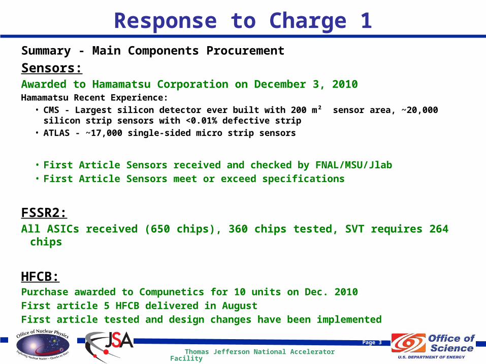
Response to Charge 1Summary - Main Components Procurement
Sensors:Awarded to Hamamatsu Corporation on December 3, 2010Hamamatsu Recent Experience:
• CMS - Largest silicon detector ever built with 200 m² sensor area, ~20,000 silicon strip sensors with <0.01% defective strip
• ATLAS - ~17,000 single-sided micro strip sensors
• First Article Sensors received and checked by FNAL/MSU/Jlab• First Article Sensors meet or exceed specifications
FSSR2:All ASICs received (650 chips), 360 chips tested, SVT requires 264 chips
HFCB:Purchase awarded to Compunetics for 10 units on Dec. 2010
First article 5 HFCB delivered in August
First article tested and design changes have been implemented
Thomas Jefferson National Accelerator Facility
Page 4
Summary – Fabrication Plan
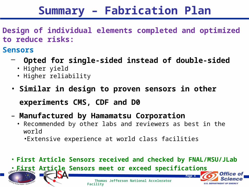
Design of individual elements completed and optimized to reduce risks:
Sensors – Opted for single-sided instead of double-sided
• Higher yield• Higher reliability
• Similar in design to proven sensors in other experiments
CMS, CDF and D0
– Manufactured by Hamamatsu Corporation • Recommended by other labs and reviewers as best in the world
•Extensive experience at world class facilities
• First Article Sensors received and checked by FNAL/MSU/JLab• First Article Sensors meet or exceed specifications
Thomas Jefferson National Accelerator Facility
Page 5
Summary – Fabrication Plan
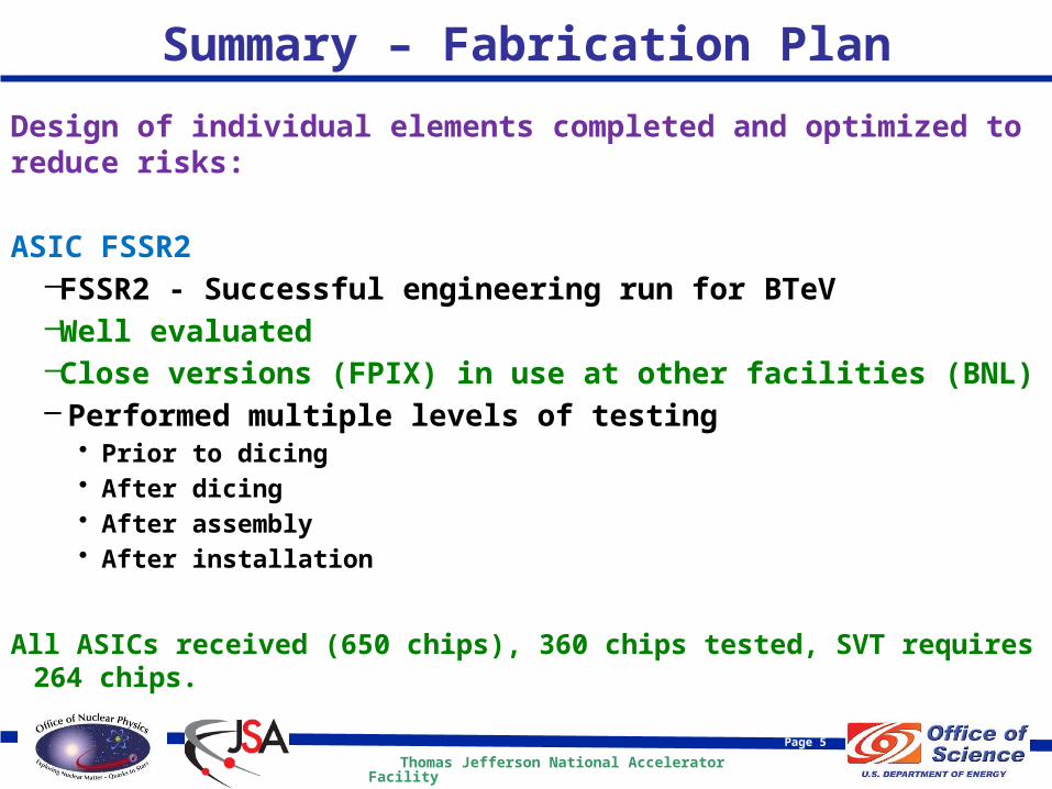
Design of individual elements completed and optimized to reduce risks:
ASIC FSSR2–FSSR2 - Successful engineering run for BTeV–Well evaluated–Close versions (FPIX) in use at other facilities (BNL)– Performed multiple levels of testing
• Prior to dicing• After dicing• After assembly• After installation
All ASICs received (650 chips), 360 chips tested, SVT requires 264 chips.
Thomas Jefferson National Accelerator Facility
Page 6
Summary – Fabrication Plan
Design of individual elements completed and optimized to reduce risks:
HFCB– Guided by designs done at CDF and D0– Designed with 3 mil trace/spacing, allowed larger group
of vendors – Researched for the best quality parts– Reviewed the design with experts in the field:
Brian Eng (JLab), Peter Bonneau (JLab), Amrit Yegneswaran (JLab), Sasha Voronin (MSU), Tim Schmitt (Compunetics),Jacoub Kurnot (Compunetics)
Electrical grade module test completed and design changes
implemented
Thomas Jefferson National Accelerator Facility
Page 7
Summary – Fabrication Plan
Fabrication plan developed and optimized to reduce risks•Module components
– Carbon fiber, Rohacell — standard materials– First electrical grade module has been fabricated– Mechanical grade module will be fabricated
•Slow Controls and DAQ–Software
Plan to use existing software LabView/Epics/CODA–Hardware
Plan to use, wherever possible, “off-the shelf” electronics•For reliability and dependability
Electronics developed for other Halls, Hall D•With an eye to standardization
Thomas Jefferson National Accelerator Facility
Page 8
CHARGE 2
Are the test measurements, both performed to date and planned, appropriate to predict the performance of the system? Will the performance provide adequate margin for operation under the expected conditions following the 12 GeV upgrade? Are plans for handling the expected radiation damage well-developed and adequate to the task?
YES
Thomas Jefferson National Accelerator Facility
Page 9
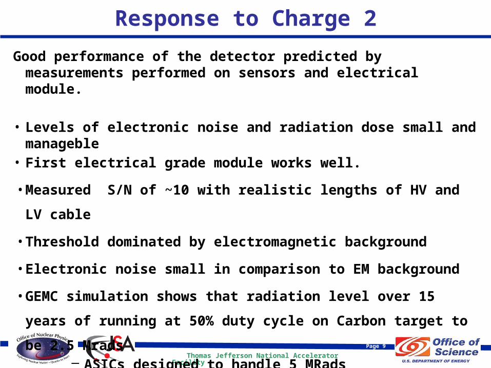
Response to Charge 2
Good performance of the detector predicted by measurements performed on sensors and electrical module.
• Levels of electronic noise and radiation dose small and manageble• First electrical grade module works well.
• Measured S/N of ~10 with realistic lengths of HV and LV cable
• Threshold dominated by electromagnetic background
• Electronic noise small in comparison to EM background
• GEMC simulation shows that radiation level over 15 years of running
at 50% duty cycle on Carbon target to be 2.5 Mrads– ASICs designed to handle 5 MRads
Thomas Jefferson National Accelerator Facility
Page 10
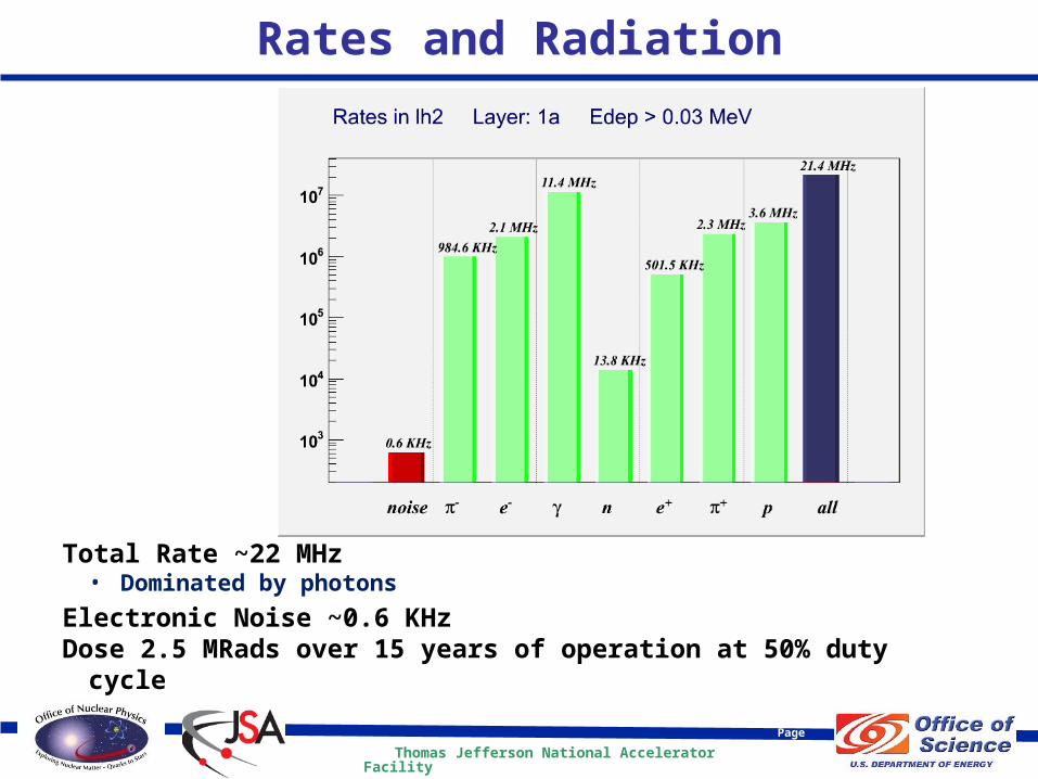
Rates and Radiation
Total Rate ~22 MHz• Dominated by photons
Electronic Noise ~0.6 KHzDose 2.5 MRads over 15 years of operation at 50% duty cycle
Thomas Jefferson National Accelerator Facility
Page 11
Charge 3
Are plans for the assembly, quality control, and acceptance testing at various sites well developed and appropriate for production of a detector of this scale?
YES
Thomas Jefferson National Accelerator Facility
Page 12
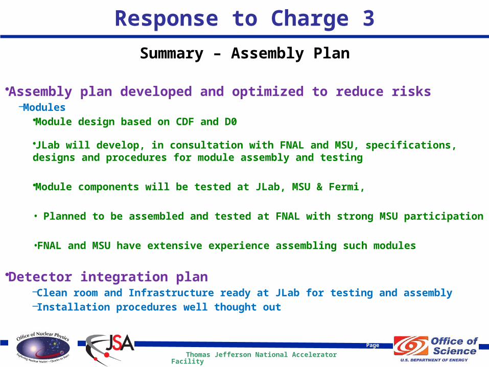
Response to Charge 3
Summary – Assembly Plan
•Assembly plan developed and optimized to reduce risks–Modules
•Module design based on CDF and D0
•JLab will develop, in consultation with FNAL and MSU, specifications, designs and procedures for module assembly and testing
•Module components will be tested at JLab, MSU & Fermi,
• Planned to be assembled and tested at FNAL with strong MSU participation
•FNAL and MSU have extensive experience assembling such modules
•Detector integration plan–Clean room and Infrastructure ready at JLab for testing and assembly–Installation procedures well thought out
Thomas Jefferson National Accelerator Facility
Page 13
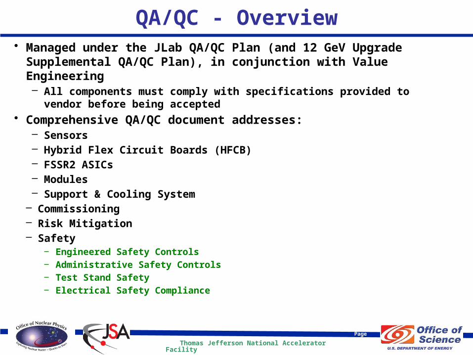
QA/QC - Overview• Managed under the JLab QA/QC Plan (and 12 GeV Upgrade Supplemental
QA/QC Plan), in conjunction with Value Engineering– All components must comply with specifications provided to vendor before
being accepted • Comprehensive QA/QC document addresses:
– Sensors– Hybrid Flex Circuit Boards (HFCB)– FSSR2 ASICs– Modules– Support & Cooling System
– Commissioning– Risk Mitigation– Safety
‒ Engineered Safety Controls‒ Administrative Safety Controls ‒ Test Stand Safety‒ Electrical Safety Compliance
Thomas Jefferson National Accelerator Facility
Page 14
Quality Assurance
• Protocols provided for situations that might compromise the detector
• Assemble and rework will be carried out in a class 10,000 clean room
• ESD protection requirements specified in NASA STD-8739.7 will be followed
• All equipment will be grounded• Grounded static dissipative mats will be used• Electronic travelers will be used for test activities• Test results are documented in the electronic
logbook
Thomas Jefferson National Accelerator Facility
Page 15
Quality Control
• Individual components will be tested prior to assembly– Silicon sensors, readout chips, PCBs, cabling …
• Complete modules will be tested prior to detector assembly
• Entire detector will be tested after assembly– On a region by region basis – and as complete detector
• Detector will be tested after installation

Thomas Jefferson National Accelerator Facility
Page 16
Value Engineering
One silicon sensor size • Design minimizes number of masks needed• Three mask designs for SVT• All SVT detector modules are identical
All detector modules are identical– Lower number of spares needed – Interchangeability between regions
Use of previously designed readout chips • Performance already evaluated
Use of Jefferson Lab developed CODA for data acquisition software
Use of Jefferson Lab developed monitoring software
Thomas Jefferson National Accelerator Facility
Page 17
Risk Mitigation
Custom fixture to prevent shipping damage
Alignment markers on support structure for installation
Fiducial marks for silicon component alignment
Standard single-sided, 320 µm silicon sensors
FSSR2 readout ASICs – Already evaluated
Thomas Jefferson National Accelerator Facility
Page 18
Risk Mitigation
Hybrid Flexible Circuit Board and instrumentation designs– Based on CDF and D0 designs
Minimal number of sensor types
Wherever possible– Industry-designed boards and electronics– “Off-the-shelf” board components
Thomas Jefferson National Accelerator Facility
Page 19
Charge 4
Is the cooling system design ready for first-article manufacture, and is it well-integrated into the design of the detector? Assess the design maturity for services and cable routing, including bias, data links, cooling services, support/mounting points, ability to provide servicing over the life of the detector, and ability to repair/replace a damaged module.
YES
Thomas Jefferson National Accelerator Facility
Page 20
Response to Charge 4
• FEA calculations performed• First mockup done of cold plate completed• Cable routing cooling services layout developed.
Thomas Jefferson National Accelerator Facility
Page 21
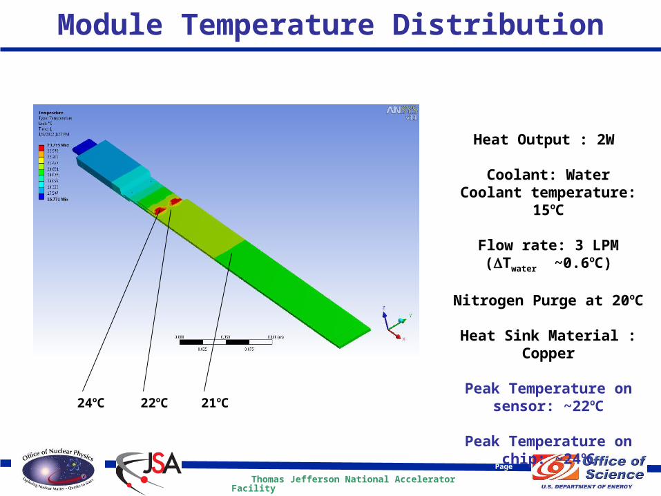
Module Temperature Distribution
Heat Output : 2W
Coolant: WaterCoolant temperature: 15oC
Flow rate: 3 LPM(Twater ~0.6oC)
Nitrogen Purge at 20oC
Heat Sink Material : Copper
Peak Temperature on sensor: ~22oC
Peak Temperature on chip: ~24oC
24oC 22oC 21oC
Thomas Jefferson National Accelerator Facility
Page 22
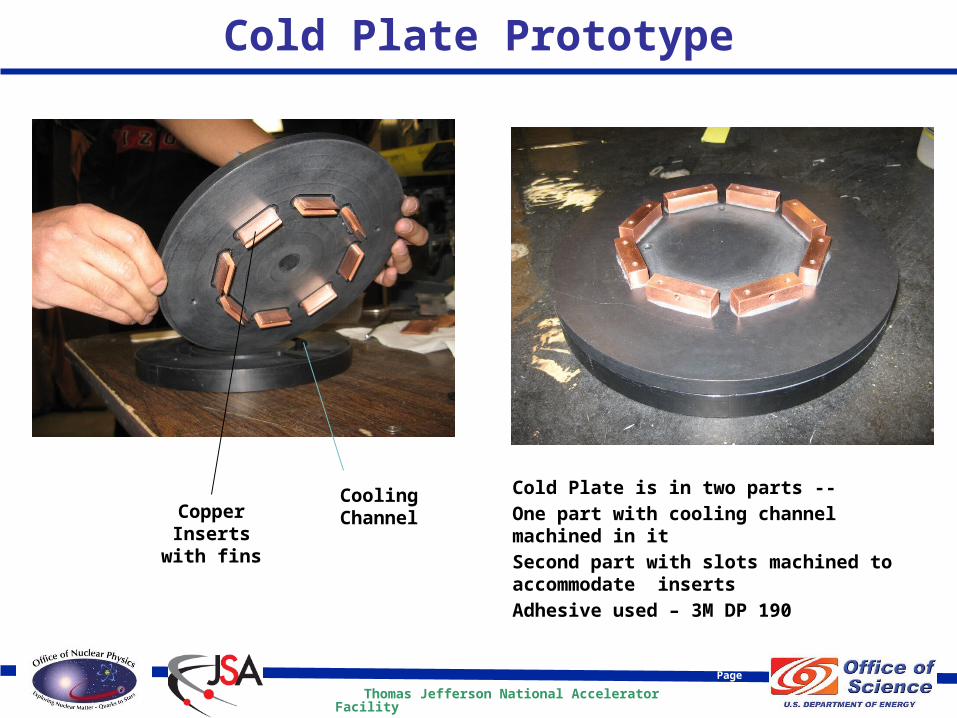
Cold Plate Prototype
Copper Inserts with fins
Cooling Channel
Cold Plate is in two parts --
One part with cooling channel machined in it
Second part with slots machined to accommodate inserts
Adhesive used – 3M DP 190
Thomas Jefferson National Accelerator Facility
Page 23
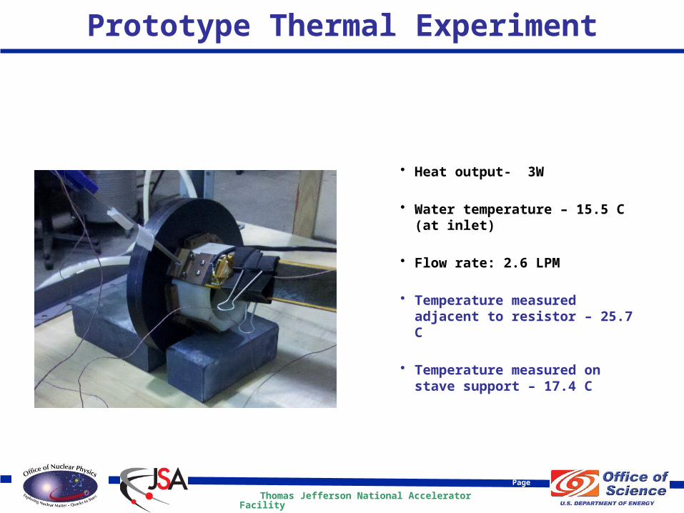
Prototype Thermal Experiment
• Heat output- 3W
• Water temperature – 15.5 C (at inlet)
• Flow rate: 2.6 LPM
• Temperature measured adjacent to resistor – 25.7 C
• Temperature measured on stave support – 17.4 C
Thomas Jefferson National Accelerator Facility
Page 24
Summary and Path Forward• QA/QC developed for each component
– Specification, assembly, and test procedures documented
• All components have been tested individually and in full chain and meet our physics specifications
• Assembly plan and acceptance testing at FNAL and JLab have been developed and documented
• Path Forward– Give the go ahead to Hamamatsu for sensor production
– Production of the HFCB with the new design changes
– Complete design of the fixtures and tooling for module production at FNAL
– Build mechanical grade module
– Start SVT module production

Thomas Jefferson National Accelerator Facility
Page 25
THANK YOU!

Thomas Jefferson National Accelerator Facility
Page 26
Appendix
Thomas Jefferson National Accelerator Facility
Page 27
Sensors: QA
• Information to be supplied by the vendor for each sensor:– ID # engraved in the area provided on the sensor– Sensor ID numbers listed for each wafer – Traceability data: relative yield of a batch, start and end
dates of processing, and wafer numbers– Test results for each sensor
Thomas Jefferson National Accelerator Facility
Page 28
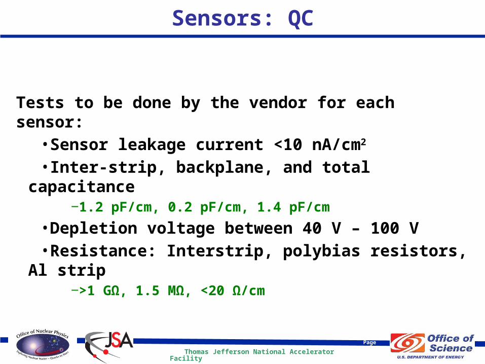
Sensors: QC
Tests to be done by the vendor for each sensor: •Sensor leakage current <10 nA/cm2
•Inter-strip, backplane, and total capacitance ‒1.2 pF/cm, 0.2 pF/cm, 1.4 pF/cm
•Depletion voltage between 40 V – 100 V•Resistance: Interstrip, polybias resistors, Al strip
‒>1 GΩ, 1.5 MΩ, <20 Ω/cm
Thomas Jefferson National Accelerator Facility
Page 29
Sensors: Risk Mitigation
Opted for single-sided instead of double-sided• Higher yield• Higher reliability
Similar in design to proven sensors in other experiments• CMS, CDF, and D0
Manufactured by Hamamatsu Corporation • Recommended by other labs and reviewers as best in
the world•Extensive experience at world class facilities
Thomas Jefferson National Accelerator Facility
Page 30
HFCB: QA• Design Phase
– Develop prototype design– Fabricate hybrid test board – Develop software to test circuit
• Vendor
– Evaluates design files– Made change suggestions– Submitted changes for approval prior to
manufacturing• Post manufacturing
– Vendor performs electrical test on all circuits for shorts and opens, rejecting all that do not pass
– Vendor sends only HFCBs that meet specifications
Thomas Jefferson National Accelerator Facility
Page 31
HFCB: QC
• Prior to population– Circuits are visually inspected using microscopes
and video capture– Circuits are tested by manufacturer for plane shorts
and voltage drop• Post component population, prior to ASIC mounting
and bonding– Circuit is power tested
• Post ASIC mounting and Bonding– Chip functionality testing
‒ Chip register test‒ Threshold scan

Thomas Jefferson National Accelerator Facility
Page 32
HFCB Installation: QC
• After installation on module– Functionality test
‒ Performed after every bonding step for 1st Article modules‒ After final sensor bonding step for production modules
– HFCB has pulse injection circuit for ASIC testing
Thomas Jefferson National Accelerator Facility
Page 33
HFCB: Risk Mitigation
• Risk– Complexity of design– Component reliability
• Mitigation – Guided by designs done at CDF and D0– Designed with 3 mil trace/spacing, allowed larger group
of vendors – Took the “next logical step” in design improvements – Researched for the best quality parts– Electrical grade module test
Thomas Jefferson National Accelerator Facility
Page 34
ASIC: QC
• FSSR2 configuration register and read-back– Data read back must be identical to written data
• FSSR2 registers’ mask load and read-back– Test mask configuration
• Threshold scan• Gain and noise measurement• Readout configuration test• Channel inefficiency• ADC operation

Thomas Jefferson National Accelerator Facility
Page 35
ASIC Risk Mitigation
• Risks– Available ASICs are only from BTeV engineering
run• Mitigation
– FSSR2 - Successful engineering run for BTeV– Perform multiple levels of testing
• Prior to dicing• After dicing• After assembly• After installation
– 650 chips in hand and 360 have been successfully tested
Thomas Jefferson National Accelerator Facility
Page 36
Backing Structure: QC / Risk Mitigation
• Visually inspect for: – de-lamination– loose carbon strands– general condition
• Measure with CMM dimensions– At least 20 points– copper heat sink flatness at 10 points with CMM
• Check – alignment holes for tolerances
• Risk Mitigation– Use of standard materials– Achievable tolerances

Thomas Jefferson National Accelerator Facility
Page 37
Module: QC / Risk Mitigation• Prior to assembly
• Visual inspection of the backing structure• Measure all dimensions of the backing structure
• Post Assembly• Dimensions of the module, flatness, straightness, etc.
will be measured and recorded using CMM• Positional accuracy of the sensors and HFCB will be
measured using an optical CMM• Check HV/LV• Measure leakage current
Risk Mitigation• Modules will be fabricated at FNAL, which has extensive
experience in fabricating and assembling similar modules
Thomas Jefferson National Accelerator Facility
Page 38
Barrel Assembly: QC / Risk Mitigation
• Cold plate will be compared to drawing specifications• Heat sink insert will be checked for compliance with
drawings and excess glue will be removed• Module support and conductor will be checked with a
CMM• Downstream support ring will be measured and
compared with the drawings
• Risk Mitigation– Cold plate prototyped– 1st Article tests

Thomas Jefferson National Accelerator Facility
Page 39
Detector Assembly: QA/QC/Risk Mitigation
• At manufacturer• All assembly components are inspected by the
manufacturer and must meet all drawing specifications
• Prior to detector assembly (of each sub-detector)• Visual inspection of the assembly components• Dimensions of the components, flatness,
straightness, etc. will be measured and recorded using CMM
• Positional accuracy of the sensors and HFCB will be measured using an optical CMM
• Risk mitigation• Cold plate and support structure were prototyped at
JLab and also compared to results from FEA
Thomas Jefferson National Accelerator Facility
Page 40
Slow Controls: QA/QC/Risk Mitigation• At the manufacturer
• All hardware functions fully tested
• At JLab after assembly and installation• Multiple automated LabView tests
‒ Test voltage, current, and trip setting
• Risk mitigation• Hardware purchased from known source for quality and
reliable products • Similar systems used previously in past Hall B systems
with great success
Thomas Jefferson National Accelerator Facility
Page 41
Data Acquisition: QA/QC/Risk Mitigation
• At the vendor– Electrical test performed on PCBs
• After assembly– Runs with laser source
• After installation– Runs with cosmic ray source– Burn-in test
• Risk mitigation– Use of “off-the-shelf” components/industry standards
Thomas Jefferson National Accelerator Facility
Page 42
Checkout after Installation
• Cables and electronics will be visually inspected
• Test– Continuity of signal cable connections– HV/LV power to front-end electronics– Slow controls procedures to adjust critical parameters
of the equipment
Thomas Jefferson National Accelerator Facility
Page 43
Commissioning
• Low voltage system will be checked with dummy loads
• Low voltage will be powered first, then high voltage, in appropriate steps
• Read/write tests will be performed on the ASIC registers
• Efficiency and tracking accuracy tests using cosmic rays will be performed
Thomas Jefferson National Accelerator Facility
Page 44
Summary
• Well developed general QA/QC plan
• QA/QC developed for each component
– Specification, assembly, and test procedures documented