this obsolete manual file is provided as a courtesy to you by ten-tec… · 2018-10-11 · this...
TRANSCRIPT

This obsolete manual file is provided as a courtesy to you by Ten-Tec, Inc.
Ten-Tec's service department can repair and service virtually everything we have built going back to our first transceivers in the late 1960's. It is our ability to continue offering service on
these rigs that has led to their re-sale value remaining high and has made a major contribution to our legendary service reputation.
Printed and bound copies of all manuals are available for purchase through our service department if you would prefer not to use this copy as your transceiver manual.
We can repair or service your Ten-Tec equipment at our facility in Sevierville, TN. We also offer support via telephone for all products via during usual business hours of 8 a.m. to 5 p.m. USA
Eastern time, Monday through Friday. We have a large supply of parts for obsolete products. Repairing a transceiver or amplifier yourself? Contact us for parts pricing information.
Service department direct line: (865) 428-0364Ten-Tec office line: (865) 453-7172
Service department email: [email protected] Address: 1185 Dolly Parton Parkway, Sevierville, TN 37862 USA
We have found it is most effective for us to help you troubleshoot or repair equipment with a consultation via telephone rather than by email.
Suggested contact methods are:
Troubleshooting or repairing equipment – call (865) 428-0364Other inquiries – call (865) 428-0364 or email [email protected]
THANK YOU AND 73 FROM ALL OF US AT TEN-TEC

lrdr
OPE
tl|l
Rrs
L
TEN I TEG
OMNI VI PLUS
MODEL564
HF TRANSCEIVER
1-1
l-2l-Jt-41-5
1-61-71-8
t-91-1 0
1-11
r-12l-13
2. GETTING STARTED
INTERFACING OTHER TEN-TEC EQUIPMENT.. .....1-4INTERFACING WITH NON TEN-TEC AMPLIFIERS............................ 1 -4STABILITY AT TURN-ON .................. 1-4
a1L-l') ',
^a
2-4
Part No. 74253lst Printing 0l/97Printed in U.S.A.
2-5

3. DETAILEDOPERATING INSTRUCTIONS
3-43-5
3-l
)-z
3-3
Part No. 74253lst Printing 0l/97Printed in f],S.A.
,t
4. CIRCUIT DESCRIPTIONS AND ILLUSTRATIONS
TNTRODUCTION..... .........4_1DC POWERINPUTBOARD (81s91)..... ..............4_lLOW PASS FTLTER BOARD (81s92)..... ..............4_2FRONT END BOARD (81s93).......... ....................4_49 MHZ CRYSTAL FTLTER BOARD (8 1 782)..... ....4_6PASS BAND TUNTNG BOARD (81781)..... ......... 4_7rF/AF BOARD (81602)..... .4_r0s.0-5.5 MHZPLL BOARD (81599). ....4_r2XTAL OSC./LO MrXER BOARD (81595)..... ....... 4_14CONTROL BOARD (81s96)..... ..........4-16LOGrC BOARD (81606)..... ................ 4_18LED DTSPLAYBOARD (81587)................. ..........4_2r
4-l4-24-34-44-54-64-74-84-94-r04-tl4-12
Part No. 74253lst Printing 0l/97Printed in U,S,A, tu

4-t34-t44-154-164-174-184-194-204-21
5. COMPUTER INTERFACE
5-l5-25-3
5-45-55-65-7
rNTRODUCTrON...... .......5-lSETTING UP THE SOFTWARE ......... 5- IOMNI VI PLUS SEzuAL INTERFACE TECHNICALDOCUMENTATION ......... 5.2RESPONSE STRINGS - RADIO TO COMPUTER....... ........ 5-3DATA FORMATS .............. 5-3COMMANDS............. ...... 5_4EXPANDED COMMANDS FOR MODELS 563 AND 564 ONLY......... 5- I O
6. TROUBLESHOOTING PROCEDURES
Part No. 74253lst Printing 0l/97Printed in U.S.A.
lv

LIST OF ILLUSTRATIONS
FIGURE
1- I DC POWER CABLE CONNECTIONS........ ............ I - 1
I-2 MICROPHONE CONNECTION... ..,...,.,1-2I -3 BUILT-IN ELECTRONIC KEYER............... ,,.,..,,.....1.2l-4 6.3 MHzIF FILTER INSTALLATION........ ............... 1-3i -5 9 MHzIF FILTER INSTALLATION........ .................. I -3t-6 votcE BOARD INSTALLATION........ .................... I -4r-7 QSKHOOK-UPWrTHHERCULESIrAMPLIFrER........ ......... l_5I -8 QSK HOOK-UP WITH CENTAUR, CENTURION OR
TITAN AMPLIFIER............... .................. I _5
1-9 QSK HOOK-UP WITH HERCULES II AMPLIFIERAND 253 ANTENNA COUPLER ........... 1-6
1- 1O HOOK-UP WITH NON TEN-TEC AMPLIFIERS............. ........ I-7
3- 1 MODEL 564 FRONT VrEW.... ................3_r23-2 MODEL 564 REAR VIEW....... ................3-123-3 MODEL 564 TOp VEW......... ..................3_133-4 MODEL 564 BOTTOM VIEW ................ 3_14
4-t DC rNpUT BOARD (81591)..... .............. 4_14-2 DC rNpUT BOARD SCHEMATTC (S 1591) .............. 4_ I4-3 LOW pASS FTLTER BOARD COMPONENT LAYOUT (81 s92)................ 4_24-4 LOW PASS FILTER BOARD COMPONENT SCHEMATIC (S1 592).......,..4-34-s BPF/FRONT END BOARD COMPONENT LAYOUT (81593)..... .............. 4_44-6 BPF/FRONTEND BOARD COMPONENT SCFIEMATIC (81593)....... 4-54-7 9WIzIF FILTERBOARD SCHEMATIC (81782)................................... 4-74-9 pBT BOARD COMPONENT LAYOUT (8 17S 1 ). ................... 4_ 84-r0 PASS BAND TUNTNG BOARD SCFIEMATIC (81781)................. ......... 4_s4-r r IF/AF BOARD COMPONENT LAYOUT (8 1602)..... ............ 4- 1 04-r2 rF/AF BOARD SCHEMATTC (81602)................. ...4_rr4-r3 s.0-5.5 wrzPLL BOARD coMPoNENT LAYour (81599).... ..........4-t24-14 5.0-5.5 MHz PLL BOARD SCIIEMATIC (S 1599).............. ....4-t34-T5 XTAL OSC.-L.O. MDGR BOARD COMPONENT LAYOUT (81595). . 4-144-r6 XTAL OSC.-L.O. MDGRBOARD SCHEMATTC (81595)................. .....4-rs4-r7 CONTROL BOARD COMPONENT LAYOUT (81596). ....... 4_164- 1 8 CONTROL BOARD SCFmMATIC (81596)................. ........... 4_174-19 LOGrC BOARD COMPONENTLAYOUT (81606)..... .......... 4_ l94-20 LOGrC BOARD SCF{EMATTC (81606).............. ..4_204-2r LED DrSpLAy BOARD COMPONENT LAYOUT (8 1587)..... ............... 4_2r4-22 LEDDISPLAYBOARDSCHEMATIC(81587)......... .............4-21
Part No. 74253lst Printing 0l/97Printed in U.S.A.
4-23 LED DISPLAY DRIVER BD. COMPONENT LAYOUT (81588).. ...............4-22
4-24 LED DISPLAY DRIVER BOARD SCHEMATIC (81588). ..........4-22
4-2s TX AUDIO BOARD COMPONENT LAYOUT (81597).............................. 4-24
4-26 TX AUDIO BOARD SCHEMATIC (81597)........... .. 4-25
4-27 LOW LEVEL DzuVERAI.B. BOARD COMPONENT LAYOUT (81608)... 4-27
4-28 LOW LEVEL DRIVERA{.B. BOARD SCHEMATIC (81608). ....4-274-29 POWER AMPLTFIER COMPONENT LAYOUT (8 1 6l I )............ ............. 4-294-30 POWER AMPLIFIER SCHEMATIC (8161 1)............... ............... 4-29
4-3t FM BOARD COMPONENT LAYOUT (81598)........... .............. 4-3 1
4-32 FM BOARD SCHEMATIC (81598) ........ 4-31
4-33 KEYPAD/ENCODER BOARD COMPONENT LAYOUT (81 589)............. 4-324-34 KEYPAD/ENCODER BOARD SCHEMATIC (8 I s 89). .............. 4-3 3
4-3s SWTTCH BOARD COMPONENT LAYOUT (81603) ................4-344-36 SWTTCH BOARD SCHEMATIC (81603) .................4-344-37 UPPER POT. BOARD COMPONENT LAYOUT (81604)..... .... 4-354-38 UPPERPOT. BOARD SCHEMATIC (81604)..... ......4-354-39 LOWER pOT. BOARD COMPONENT LAYOUT (81605)..... .. 4-364-40 LOWERPOT. BOARD SCHEMATTC (81605)..... ....4-36
5-1 CONNECTION OF OMNI VI PLUS TO COMPUTER....... ......5-I5-2 RS CABLE WIRING CONNECTIONS........ ............ 5-1
Part No. 74253lst Printing 0l/97Printed in U.S.A. v,

INTRODUCTION
The OMNI VI Plus is the culmination oftwodecades of engineering in high performance HFtransceivers.
The OMNI VI Plus features an advancedphase locked loop synthesizer combined with anoven timebase controlled crystal mixed oscillatorfor superior phase noise performance and stability.A large LED display is used for ease of viewingthe operating frequency. Two additional smallerdis-plays for a 12 hour clock and zuTD(T offset. are
included. The ON{NI Vl Plus also provides 100duplex memories (stores both VFOs. mode andfilter settings), scratch pad memory, band regis-ters, dual VFOs. direct frequency entry as well as
single button band change and a built-in iambickeyer (mode A or B).
The OMNI VI Plus covers all amateurbands.I 60 through l0 meters. using CW lwith full or semibreak-in), SSB (with built-in speech processor).
RTTY (true FSK or AFSK), and FM.Optional crystalfilters can be installed in both the 6.3 MHz pass
band tuning and 9 MHz IF's.The OMNI VI Plus utilizes Digital Signal Pro-
cessing for several receiver functions. This tech-nology provides an automatic notch filter, noisereduction. progammable CW hansmit offset withtracking sidetone and an audio lowpass filter.
Chapter I ofthis manual covers installation and
available accessories. Chapter 2 covers basic op-eration ofthe transceiver in orderto quickly placethe OMNI VI Plus in operation. Chapter 3 pro-vides more detailed operating instructions. Chap-ter 4 provides all ofthe technical information andschematics. Chapter 5 provides detailed informa-tion about the computer interface. Chapter 6 pro-vide some hints for troubleshooting. should a prob-lem arise.
UNPACKING
Examine your OMNI VI Plus for signs ofshipping damage. Should any damage be ap-parent, notify the delivering carrier immedi-ately, stating the full extent of the damage.
Retain all damaged cartons. Liability forshipping damage rests rvith the carrier. It is rec-ommended you keep the shipping carlon and fill-ers in the event that storage, moving. or reship-ment becomes necessary.
The following hardrvare and accessories arepacked with your OMNI VI Plus. Make surethat you have not overlooked anything. If any of the previous items are missing,
contact the repair department at Ten-Tec forreplacements:
Repair Depaftment ................ ... 423 -428-0364Switchboard............... 423-453-7172FAX......... 423-428-4483
l - #380881 - #380s7
4 - #41020r -#740201 -#742531 -#74234
I - #860551 - #27045
.062" Allen Wrench4-pin Power CableConnectorFemale Terminal PinsWarranty CardOperator's ManualOMNI VI PlusConnections GuideDC Power CordSpare 25A AGC Fuse
3 - #3s003I - #35057| -#35263
I - #38040
Part No. 7.1253
lst Printing 0l/97Printed in U.S.A.
Phono Plug4-Pin Mic Connector1/8" Stereo plug foriambic keyerpaddles.050" Allen Wrench
vu

Model 564 SPECIFICATIONS
MODES USB, LSB, CW' FSKOTAFSK, FM.
FREeUENCYRANGE All ham bands 160 through l0 meters, twelve 500 kHz segments with
30 kHz over-shoot at upper and lower band edges.
DISpLAy 7 digit to l0 Hz resolution, .56" LED,2 secondary .3" displays for clock,
memory channel and offset.
FREQUENCY CONTROL LO generated with a crystal oscillator mixed with a low noise 4.97 - 5.53
MHz phase locked looP.
OFFSETTUNING
DUAL VFO's
MEMORIES
PCINTERFACE
ANTENNA
DIMENSIONS
WEIGHT
FREeUENCY ACCURACY +l- 50 Hz @ 25 degrees C. (NOTE: The frequency will shift noticeably forl-2 minutes while the oven heats up when first turned on. Leave DC power
connected to the rear panel to eliminate this turn-on drift).
50 ohm unbalanced.
REMOTEBANDSWITCHING Rear panel band outputs for selecting antennas or other station accessories.
POWER REQUIRED 2 A receive, 20A transmit @ 12-15 VDC.
CONSTRUCTION 20 Gl0 epoxy glass PC boards, most field replaceable. Extruded aluminum
front panel, aluminum chassis, texture painted top and bottom. snap up stain-
less steel bail.
+l-9.99 kHz, receive andtransmit.
with SPLIT mode
100 duplex memories, one scratch pad memory @attery backup, 2-3 yr. life)
Serial port operation of receive and transmit. RS-232 and ICOM@ compatible
TTL interface are provided. Runs at 1200, 2400, 4800, 9600, or I 9200 baud'
HWD 5.75" x 14.75" x 17" - 14.6 x 37.5 x 43.2 cm.
l6 lbs. - 7.25kb
TRANSMITTER
RFOUTPUT
DCINPUT
SPEECHPROCESSOR
0-100 watts, ALC stabilized
Maximum 250 watts @ I4VDC. 100% duty cycle for up to 20 minutes.
Continuous duty with customer supplied air cooling of rear panel heat sink.
MICROPHONE INPUT 200-50K Ohms, accepts microphones with -67dB (0 dB : lV/microbar)output. Polarizing voltage for electrets provided
Adjustable compression level.
Part No. 74253lst Printing 0l/97Printed in U.S.A.
vlll

T/RSWITCHING
IAMBICKEYER
CWOFFSET
FMDEVTATION
METERING
SSB GENERATION
CARRIER SUPPRESSION
UNWANTED SIDEBANDSUPPRESSION
THIRD ORDER INTERMOD
SPURIOUSOUTPUT
PTT or VOX on SSB, switchable FAST or SLOW QSK on CW, delay on
SLOW is adjustable.
Adjustable l0 - 60 WPM, type A or B, weight adjustable from keypad.
Programmable 400 - 990 Hz, DSP generated, sidetone automaticallymatches offset, volume adjustable independent of AF gain control.
+l- 5 kllz
Switchable to forward power, SWR, collector current or audio processinglevel on SSB.
Balanced modulator followed by 9 MHz,8 pole crystal ladder filter.
60 dB typical
60 dB typical at 1.5 kHz tone.
30 dB below two tone at 100 watts PEP.
Better than 45 dB below peak power output.
RECEIVER
SENSITIVITY MODESSB, CW, FSK
FM0. 16 uV for l0 dB SNR @ 2.4 kHz0.35 uV for 12 dB SINAD
SELECTMry
FILTERCOMBINATION TYPICAL SYSTEM BANDWIDTH
@-6 dB @-60 dB9 MHz IF2.4kllz2.4kLIz2.4kIIz2.4kllz1.8 kHz*500 Hz*250H2*
PBTIF2.4UJIZ1.8 kHz*500 Hz*250llz*l.8kHz*500H2*250llz*
2.4kHzl.8kHz500llz250H2l.TkIIz350112
l90IIz
3.2kHz2.7 kLlz1.3 kHz850 Hz2.4kllz900tlz550 t{z
Shaoe Factor
1.30
1.50
2.60
3401.40
2.60
2.90
Optional Jilter is required
D\T{AMICRANGE
THIRDORDERINTERCEPT
NOISEFLOOR
PHASENOISE
S-METER
97dB @2.4 kHz bandwidthat20 kHz spacing,
+l0dBm
- I 33dBm @2.4 kHzbandwidth
-l22dBc @ I kHz, - 138dB c @20 kHz
Calibrated for 59:50 uV
100d8+ with CW filters
Part No. 74253lst Printing 0l/97Printed in U.S.A.
tx

ATTENUATOR
PASSBANDTUNING
IFFREQUENCIES
NOISEBLANKER
AUTOMATIC DSPNOTCHFILTER
MANUALNOTCH FILTER
DSPNOISE REDUCTION
DSPFILTER
RECEIVERECOVERYTIME
SQUELCHSENSITIVIry
IMAGEREJECTION
I-FREJECTION
AUDIO
SEPARATE RXANTENNA INPUT
-20dB
+l- 1.5kHz
I st IF 9MHz, 2nd IF 6.3MHz (passband tuning IF), 2nd IF for FM 455KHz'
Adjustable threshold
Eliminates multiple heterodynes, notch depth automatically selected for each.
200 Hz to 2.5 kHz, greater than 5 OdB. Adjustable center frequency.
Auto-correlation type algorithm. Broadband noise reduction of 5 to l5dB istypical depending on conditions.
Lowpass audio filter selectable in 5 steps, 1400 H2,1200 H2,1000 Hz, 800 Hz,
600H2, ormay be disengaged.
less than 20 ms including split mode.
less than .6uV
>90d8
>90dB
1.5 watts @ 4 ohms with less than2 o/o distortion, built-in speaker. separate
fixed output I mw @ 600 ohms.
50 ohm phonojack, frontpanel selectable.
Part No, 74253lst Printing 0l/97Printed in U.S.A.

CHAPTER 1
INSTALLATION
1-1 POWER SUPPLY The OMNI YI Plusrequires a source of well filtered and regulatedDC voltage. The supply voltage can range from+12.0 to +15.0 VDC but an optimum of +13.8
VDC is recommended. The voltage source mustbe capable of 22 amps.
The TEN-TEC Model 962matching powersupply is specifically designed for this service.This supply has built-in over current protectionand all of the necessary RFI bypassing. TheModel 962 also has a front facing speaker. Toactivate this speaker, plug the ll4" phone plugfrom the power supply into the EXTERNALSPEAKER jack on the rear panel of the OMNIYI Plus.
The four pin DC connector on the rear panel
of the OMNI YI Plus is polarized such that themating plug will only attach in one direction.With the Model 962, simply determine the cor-rect orientation and plug the power cable intothe OMNI YI Plus.
If an alternate power source is to be used,we recommend that the preassembled DCpower cord (p/n 86055) be used. We have alsoincluded spare connector pins (p/n 41020) anda connector shell (p/n 38057) for building yourown cord. Be sure to use no less than 14 gaugestranded wire for these connections because ofthe high current demand during transmit.
+ 12 to 14 VDC
REAR VIEWOF
TRANSCEIVER
GROUND
FIGURE I.1DC POWER CABLE CONNECTIONS
Part No. 74253lst Printing 0l/97Printed in U.S.A.
NOTE: Always enable the power source
first and then the lransceiver.
If the DC pohter source is supportedby a generotor or olternotor, alwaysturn off the trsnsceiver before theequipment is started or shut offThese recharging devices can oftengenerote large voltage spikes thatmight domage the transceiver
l-2 ANTENNAS The transmitter is protectedagainst damage from load impedance mis-matches ranging from a dead short to an opencircuit. Operation at or near full power is pos-sible with an unbalanced (coax feed) load im-pedance between 25 and 100 ohms (approxi-mately 2:1 SWR). Antennas with higher SWR,or single wire and balanced feedline types, willrequire the use ofan external antenna tuner forbest results.
NOTE: When operating the transmitter intoan SWR higher than 2:1, adjust the RF "PWR"control lo a collector (Ic) current not to exceed20 amps as indicated on the front panel meter.
The main antenna connection to the trans-ceiver is through the rear panel SO-239 con-nector. In most installations, this connection willcarry both transmit and receive signals and thefront panel receive ANT switch will be set toMAIN. If a separate receive antenna is to beused, connect it to the rear panel AUX RX AN-TENNA jack. You can leave both antennas con-nected at all times and select the desired receiveantenna with the ANT selector pushbutton.

1-3 MICROPHONES Any TEN-TEC micro-phone, using our four pin connector, may be
used without modification. Most dynamic, ce-
ramic, crystal or electret type microphones may
also be used. When adapting another micro-phone, please refer to the connector wiring dia-
gram in FIGURE l-2. A spare four pin micro-phone plug (p/n 35057) is included in the pack-
ing kit. Be sure to use shielded cable to prevent
any RF interference. Electret types and some
with built-in preamplifiers will require the DCvoltage available at pin 4.
'-1,]Qt o"o
,\"" o'/l*r \'-;/ ",.VDC
FRONT VIEW OF 564
FIGURE 1-2
MICROPHONE CONNECTION
1-4 CW KEY Two methods are available forkeying the transceiver in CW mode. The rear
panel KEY phono jack can be connected to astraight key, bug, or external keyer. A connec-
tion between the center pin and the ground willkey the transmitter.
The OMNI YI Plus also features a built-iniambic keyer. The rear panel 1/8" stereo jack
labeled KEYER allows connection to any style
of keyer paddle. Refer to FIGURE 1-3 and use
the plug
DAH
GND \
t
FIGURE I-3BUILT.IN ELECTRONIC KEYER
CONNECTION(pt1n35263) supplied in the packing kit. The
keyer speed is controlled by the front panel
KEYER SPEED control. See Chapter 3, Sec-
tions 3-1.13 and 3-4 formore details regarding
the use of the built-in keyer.
l-5 STATION GROUND A good ground sys-
tem is essential for optimum operation of any
transmitter. The best solution is to connect allthe station equipment chassis together using a
heavy flat ground braid. Use another length ofbraid to connect to a ground rod. Ifyou are notusing a linear amplifier a less ideal ground may
suffice. A ground connection to the copper cold
water plumbing pipe is usually acceptable.
Antenna type and the proximity to the sta-
tion are also a factor in choosing ground meth-
ods. With good resonant antennas located away
from the station, the AC ground in your house
wiring may be adequate.
1-6 CONNECTIONS FOR OTHER AC-CESSORY EQUIPMENT Connectors have
been provided to interface to a variety of sta-
tion equipment. This includes linear amplifiers,RTTY terminals, computer equipment and
phone patches. See the Table of Contents to lo-cate detailed information on how to connectvarious equipment to the OMNI YI Plus.
1.7 TEN.TEC ACCESSORIES FOR THEOMNI VI PLAS
Crystal Filters for the 9 MHz IF216 - 500 Hz 6 pole for FSK217 - 500 Hz 8 pole for CW218 - 1.8 kHz 8 pole for SSB
219 - 250H2 6 pole for CW220 - 2.4kHz 8 pole for SSB
Crystal Filters for the 6.3 MHz IF282 - 250H2 6 pole for CW285 - 500 Hz 6 pole for CW288 - 1.8 kHz 8 pole for SSB
DIT
l-I
ll
if_,),'a\., ]
rl
\),
Part No. 74253lst Printing 0l/97Printcd in U.S.A.t-2

Other Accessories236 - Remote control cable for Model420
238239257259264
Amplifier or Model 253 Tuner- 2 Kw antenna tuner- 100 Watt dummy load- Voice Synthesizer Board- ALC Annunciator- 236 expansion cable for connecting
Model 4201253 combination607 - Single Paddle Keyer Assembly701 - Hand Microphone705 - Desk Microphone962 - Matching Power SupplyRM-500 - Rack Mounting Kit35057 - 4 pin Microphone Connector80-572 - 4 pin DC Connector with pins
I-8 INSTALLING OPTIONAL FILTERSAll optional filters install either on the 9 MHzIF board orthe PBT (Pass Band Tuning) board.Refer to Figures l-4 and l-5. These boards areboth located on the bottom side of the trans-ceiver. To remove the bottom cover, set thetransceiver upside down with the front panelfacing forward. Remove two Philips screwsfrom each side of the bottom cover and slidethe cover back out from under the edge ofthefront panel extrusion.
Remove the bottom cover to expose two re-movable panels. The optional filters plug intocircuit boards underneath these panels.
l-8.1 INSTALLING 6.3 MHz IF FILTERSRemove the panel covering the PBT board.
There are three dedicated positions on the boardfor the three optional filters. Referring to Fig-ure 1-4, plug the filter into the appropriate po-sition. The filters are non polarized and may beinstalled in either direction. Replace the paneland the bottom cover.
FIGURE 1,46.3 MHz IF FILTER INSTALLATION
1.8-2 INSTALLING 9 MHz IF FILTERSRemove the panel covering the 9 MHz filterboard. There are two empty filterpositions, Op-tional Filter I and Optional Filter 2 that corre-spond to the N-l and N-2 buttons on the frontpanel. Plug the optional filter into the desiredlocation. Like the passband tuning filters, theseare also non-polarized and may be installed ineither direction. Because the various filters havedifferent amounts of loss, each position has aselectable gain jumper to compensate. Models216,217 and2l9 require the high gain setting.Models 218 and 220 use the low gain setting.Position the jumper plug to connect the correctpins on JGl and JG2 as shown in Figure 1-5.
9MHz FILTER BOARD
O JGI .""
FIGURE 1-59 MHz IF FILTER INSTALLATION
lo
o
o
PASS BAND TUNING BOARD
STANDARD O
2 4 kHz FILTERo
OPTIONAL1.8 kHz FILTER
OPTIONAL500 Hz FILTER
OPTIONAL250 Hz FILTER
Model288
Model285
Model282
J
zoF
F
zo
Part No. 74253lst Printing 0l/97Printed in U,S.A. l-3

I.9 OPTIONAL VOICE SYNTHESIZERBOARD, MODEL 257 Thevoice synthesizer
will announce the display frequency when the
VOICE button is pressed. To install the voiceboard, remove the two Phillips screws on each
side of the top cover. Slide the cover back fromunder the edge of the front panel extrusion and
lift the cover off. The voice board plugs into acard edge connector on the Logic Board. Refer
to Figure l-6. Test the operation of the voice
board by powering up the transceiver and press-
ing the VOICE pushbutton. The speech level
can be adjusted with trimmer resistor R13 on
the voice board.
NOTE: If you already own Model 257 and qre trans'
ferring it from a transceiver other than Model 563 or564 contact the factory for modification details.
To incorporate a TEN-TEC amplifier into the
station, remove the plug jumper and use
shielded cables to connect to the key lines ofthe amplifier. These connections are shown in
Figures 1-7, 1-8 and 1-9. These connections
insure that propertiming is maintained between
the transceiver and amplifier during QSK op-
eration.
I.T2 INTERFACING WITH NON TEN.TEC AMPLIFIERS Refer to figure l-10 forconnections. You must activate the relay fromUSER OPTIONS MENU #1 (see Table 3-1).
Change LCO from its default position OFF to
oN.
1.13 FREQUENCY STABILITY AT TURN.ON OMNIYI Plus transceivers incorporate a
feature to keep the crystal oven on for improvedfrequency stability. To utilize this feature, leave
the power supply ON, when the radio is OFF.
If this feature is not desired turn the power sup-
plyOFF.
oJ't \L| ./
o
o
VOICE READOUT< (option)
LOGIC BOARD
i1)
FIGURE T.6VOICE BOARD INSTALLATION
1-10 OPTIONAL ALC ANNUNCIATORM O D EL 259 This accessory allows the visionimpaired operator to adjust MIC GAIN controlproperly. Refer to the Model 259 manual for teinstallation procedure.
1.11 INTERFACING WITH OTHER TEN-TEC EQUIPMENT Two phono connectorson the rear panel of the OMNI Yl PIus allowaccess to the keying circuitry in the transceiver.
These connectors, labeled TX OUT, and TX EN,
are normally connected together with a jumperplug.
t-4
Part No. 74253lst Printing 0l/97Printed in U.S.A.

(REAR vtEw)
MODEL 420
KEY INKEY OUTRF INPUTREMOTE CONTROL
(REAR vtEtv)
MODEL 564
TX OUTTX EN50 OHM ANTENNAINTERFACE PORT
USING
SHIELDEDSHIELDED
CABLECABLE
420 rNMODE,
(REAR vtEw)
REQUIRED CONNECTIONS
MODEL 420 MODEL 564
KEY IN TX OUTKEY OUT TX ENRF INPUT 50 OHM ANTENNA
USING
SHIELDED CABLE WITH PHONO PLUGSSHIELDED CABLE WITH PHONO PLUGSRG-58/u wtTH PL-256
FIGURE 1.8. QSK HOOK.UP WITH CENTAUR, CENTURION OR TITAN AMPLIFIER
Part No. 74253lst Printing 0l/97Printed in U.S.A.
c:_:l c----------l
-:) -
--)C-] C-
rar|EY g |fI r q,l tEr stn Ft
I(D€L 56' o|IM VI PLUS
REQUIRED CONNECTIONS
RG-58/U OR EOUIVALENTMODEL 236 CABLE
FIGURE T.7. QSK HOOK-UP WITH HERCULES II AMPLIFIER
(REAR vrEw)
NOTE
PI-ACE THE MODELTHE OSK CONTROL
if0uratr
o
ffHPIJT
nooEL 564 orNt V PLUS
I|ENFET F('|I
TT OUI '|
O' ryIE PTIo o oo
l-5

rooEL 564 olrill Vl PLUS
oooooo
OO(l.---..-)(-_--)
(:----------l(:---r(--.------)
-
xtY ril r/or Fi fi qJT XEY SffI FUT
6^Ur€ED UrE t2-t. YDC oeCO sffiTr
MODEL 420 MODEL 253 MODEL 564 USING
RF INPUT 50 OHM ANTENNA RG-58,/U WITH PL-259KFY IN TX OUT -DED CABLE WITH F PLUGS
KEY OUT EXCITER CONTROL IN LDED CABLE WITH PHONO PLUGS
EXCITER CONTROL OUI TX EN HIELI]LIJ CABLL W
REMOTE CONTROL REMOTE CONTROL INTERFACE PORT MODEL 235 + MODEL 264
RF OUTPUT RF INPUT RG-8,1U OR EQUIVALENT
REQUIRED CONNECTIONS
FIGURE 1-9. QSK HOOK.UP WITH HERCULES II AMPLIFIER AND 253 ANTENNACOUPLER
Part No. 74253lst Printing 0l/97Printed in U.S.A.l-6

(REAR vrEW)
KEYING RELAY INPUT RELAY (N.0.)
(REAR vrEw)
SHIELDED CAELE
NOTE
YOU MUST VERIFY THAT THE AMPLIFIER KEY INPUTREQUIRES ONLY A LOW VOLTAGE DC CONNECTIONTO GROUND. SEE PARAGMPH 3-6.15 REGARDINGTHE RELAY OUTPUT JACK ON THE MODEL 564.
FIGURE 1.I0. HOOK-UP WITH NON TEN-TEC AMPLIFIERS
NON - OSr( ArpLrrrER YOOEL 56ir OI|NI vl PLUS
m:nfrcE P(nr
f(lnnr
tElncRTIJYiftjT
YI
I
rrPrrl
sa\ ! ifuY6665OoqoSHIELOED CTELE
AMPLIFIER
RF INPUT
REQUIRED CONNECTIONS
MODEL 564 USING
50 oHM ANTENNA RG-58/U CW KEY
Part No. 74253lst Printing 0l/97Printed in U,S.A. t-7

CHAPTER 2
GETTING STARTED
2-1 INTRODUCTION Virtually all aspects
of the OMNI YI Plus' operation are user pro-grammable from the front panel. This includesmany "set and forget" features that are accessed
through menus using the frequency display andthe keypad. All of these operator options areexplained in detail in Chapter 3. The defaultsettings, as shipped from the factory. will allowyou to get started. You can customize the op-eration to more closely fit your preferences as
you become familiar with the transceiver.
BEFORE YOU POWER UP
The first time you power up the OMNI YI Pluswe suggest doing a MASTER RESET as ex-plained in Section 2-4.2. This will clear out anymemory locations or special settings that werea result of factory burn-in and testing.
When power is first applied, the ovenizedcrystal timebase will take one or two minutesto stabilize. If you choose to leave the powersource to the transceiver on. the oven will runcontinuously and no tum-on drift will occur. SeeSection 1-13.
2-2 INITIAL FRONT PANEL SETTINGS:
RF ........... Full ClockwiseAF ........... ............9:00POWER ................ oNMETER.... FWDANT......... .........MAINAGC......... ............. oNAGC......... FASTNOTCH ....... MANUAL (no lighQQSK ......... FASTATTN ... OFF (no light)NB ........... . Full counter clockwiseSQL.......... . Full counter clockwise
Part No. 74253lst Printing 0l/97Printed in U.S.A.
P8T.......... 12:00NOTCH ....Full counter clockwiseRITDCT Ignore for nowPROC ... OFF (no light)MIC.......... ............9:00PWR 12:00KEYER SPEED Full counter clockwisePROCESSOR ............. Full counter clockwiseVOX....... OFF (no VOX light. upper display)SELECT DESIRED MODE
...... CW, LSB, USB, FSK, FMSELECT VFO "A" ................. use A/B button,
if VFO B activeSPLIT OFF (no SPLIT light
in upper display)RIT........... . OFF (no Numeric off-
set displayed. no lightXIT.......... OFF (no offset displayed, no light)LOCK . OFF (no light)SELECT DESIRED BAND
.. Use band buttonsSELECT FREQUENCY...... Use main tuning
knob or UP/DOWN Arrow keysI-F FILTER ....... Select 2.4, all filter lights off
See Figure 3-1 for location of the controls re-ferred to in the following paragraphs.
2-3 OPERATION Connect a suitable resonantantenna to the rear panel 50 OHM ANTENNAconnector. Check for received signals. Turn toa clear area of the band and press the TTINEbutton. Adjust the PWR control to the desiredoutput power. Switch the METER switch to theIc (collector current) position and check for areading of 20 amps or less. Switch to the SWRposition and check for a reading of 2:l or less.
2-3.1 SSB MODE OPERATION Select ei-ther LSB or USB and key the transceiver by
2-l
pressing the microphone's PTT (Push to talk)
button. While speaking into the microphone' ad-
vance the MIC control until the ALC LED be-
gins to flash. The LED indicates that the trans-
ceiver is generating full output power relative
to the setting of the PWR control. Try to avoid
lighting the ALC light too frequently. This in-
dicates that the transmit circuitry is being over-
driven.Tune the receiver to a SSB signal' If there
is bothersome influence, adjust the PBT (Pass
Band Tuning) control to position the receiver's
crystal filtering on the desired signal. The PBT
control can often be manipulated slightly to re-
duce interference from nearby signals.
To fine tune the receive frequency withoutchanging the transmit frequency, tum onthe RIT(Receive Incremental Tuning) function. Use the
RIT/XIT knob to adjust the receive frequency.
To clear the RIT, press the RIT button again.
See Chapter 3 for more detail on offset tuning.
2-3.2 CW OPERATION Select the CW
mode. A closure of the rear panel KEY jack toground will key the transmitter. The built in elec-
tronic keyer can also be used. If you do not want
fast break-in CW, switch the QSK pushbutton
to SLOW. Refer to Chapter 3 for more details
on other adjustments such as sidetone volume,
CW offset frequency, keyer speed and weight-
ing. If narrow CW filters have been installed,
select one and adjust the PBT control for the
best reception.
2-3.3 FM OPERATION Selectthe FM mode.
(NOTE: This mode is currently authorized by
the FCC for use between 29.0 and29.7 MHz).Press the microphone PTT button to transmit.
In this mode the MIC gain control adjusts the
amount of FM deviation rather than the trans-
mit power. With TEN-TEC brand microphones,
the MIC control should be set to 12 o'clock. You
may find a slightly higher or lower setting is
needed with other microphones.In receive, adjust the SQL (squelch) con-
aa
trol for quieting when no signal is present' The
narrow IF filters and PBT function are disabled
in FM mode. If FM repeater operation is de-
sired, set up the dual VFO's with the transmit
and receive frequencies and use SPLIT mode.
Detailed information about the dual VFO's is
in Chapter 3.
2-3.4 FSK MODE This mode places the re-
ceiver in LSB and enables the rear panel
MARIVSPACE input. A closure on either the
KEY or PTT inputs will transmit a CW carrier.
The frequency of this carrier is shifted by 190
Hz depending on the logic level of the MARK/SPACE line. Refer to Chapter 3 for more de-
tails on how to connect a modem or terminal
unit.
2-4 AFEW WORDS ON MICROPROCES-SORS On rare occasions you may find the
transceiver will not accept commands from the
keypad properly or it is operating in an erratic
manner. Spikes or surges on the power supply
line or an unforeseen set of circumstances may
confuse the microprocessor. This technology
has improved dramatically in recent years but
it is still possible to have an occasional lockup.
If turning POWER off and on does not resolve
the problem, the microprocessor must be reset
using one of the following methods.
2-4.1 PARTIAL RESET Always try thismethod first as it will not erase memories orselections from USER OPTIONS MENUS.Turn off POWER. Press and hold the CLEARbutton and turn POWER on. Continue to hold
CLEAR for several seconds and release. If this
does not return the transceiver to normal op-
eration use a MASTER RESET.
2-4.2 MLSTER RESET This will erase allmemories and return the USER OPTIONSMENUS to factory presets. Turn off POWER.
Press andhold ENTERbutton andturn POWER
on. Continue to hold ENTER for several sec-
Part No. 74253lst Printing 0l/97Printed in U.S.A.

onds and
2.5 MAIN TUNING KNOB DRAG AD-JUSTMENT The main tuning knob has aspring loaded friction pad on the back. To ad-just the amount of drag, hold the rear chromeskirt and turn the main knob body. Tum the knobcounter clockwise to loosen and clockwise totighten the amount of drag. If the chrome skirtseems a little off center relative to the keypadbezel after this adjustment, it can be shiftedslightly so that it spins evenly within the bezel.
Part No. 74253lst Printing 0l/97Printed in U.S.A.
2-3

CHAPTER 3
DETAILED OPERATING INSTRUCTIONS
3-1.00 FRONT PANEL CONTROLS - KEY-PAD FUNCTIONS (See Figure 3-l) Singlebutton selections such as band, mode, IF fil-ters, VFO selection and RITDilT operations arethe ones you will use routinely. All are wellmarked and supported with status lights. Multi-stroke keypad functions are used for less fre-quently used features or to customize the trans-ceiver to fit your personal preferences. Theseoptions are explained in the following sections.These functions tend to be "set and forget" be-yond experimenting during the initial setup.Every effort has been made to allow you to op-timize your transceiver whether you operate onemode or enjoy all of them.
When making these initial adjustments, besure to select the proper mode and frequency.We also recommend the use ofa 50 ohm dummyload (Model239),capable of at least 100 watts,during this setup procedure.
NOTE. Any of these multiple key command se-quences can be aborted before completion bypressing the CLEAR button.
3-1.01 CHANGING FREQUENCY Thereare four methods of changing frequency orbands:
l) Tune up or down the band with the maintuning knob. The knob tunes at a default rate of5.00 kHz per revolution.
Other rates are selectable by the user. Refer toSection 3-4.
2) Move up or down a band quickly in 100 kHzsteps using the I or Y arrows on the keypad.
3) Change from band to band by pressing thedesired band button.
Part No. 74253lst Printing 0l/97Printed in U,S.A.
4) Move to a particular desired frequency byentering it directly on the keypad as outlinedbelow:
Press ENTER (Display now shows dashes).Key in the desired frequency. It is not neces-sary to enter every number down to the l0Hzdigit. Pressing ENTER at any point will fill theremaining digits with zero.
Example 1: Desired frequency 14.200.00.Press ENTER, 1,4,2, ENTER.
Example 2: Desired frequency 3.786.55.Press ENTER, 3, 7, 8, 6, 5, 5. (It is not neces-sary to hit ENTER after the last digit).
Example 3: Desired frequency 1.890.00.Press ENTER, 0, 1, 8,9, ENTER. (NOTE:To enter a frequency on 160M, a "zero" mustpreceed the "one.")
The numerical keypad functions as a singlebutton bandswitch as shipped from the factory.To enter an exact frequency, you must pressENTER, then the frequency, as explained in theprevious examples. This feature may be re-versed inthe rJSER OPTIONS MENU with theFEP option (Frequency Entry Priority). If re-versed, you must press ENTER to bandswitchand an exact frequency can be typed withoutthe ENTER key to start the sequence. Refer toSection 3-4 for details.
3-1.02 TUNE Pressing the TUNE button keysthe transmitter and is equivalent to the "keydown" condition in CW. The power output levelmay be set anywhere between 0 and 100 wattsusing the PWR control. The MIC gain controlhas no effect in the TUNE mode. This provides
3-l
a convenient way to set the power level, check
SWR and collector current.
3.1-03 CW This button selects the CW mode.
First, make sure that the NOTCH pushbutton is
in the manual position andthattheNOTCH con-
trol is fully counterclockwise. This places the
audio notch down below 100 Hz where it willnot interfere with the passband. The CW mode
select button activates a SPOT tone once the
transceiver is already in CW mode. Press and
hold the CW button and use the audio tone as a
reference while you tune in the desired signal.This will position the transmit signal to precisely
match the incoming signal frequency.For transmit, a standard key or an external
keyer can be connected to the rear panel KEYjack. The built-in keyer can be activated witheither a single or dual paddle connected to the
1/8" stereo KEYER jack.
See 3-5.14 for information on selecting thereceiver QSK response. Other sections cover
setting the sidetone, adjusting the keyer and se-
lecting filters.
3-1.04 USB/LSB Selects the upper and lowersideband modes. All of the IF filters are select-
able in these modes but only the standard 2.4
kHz and optional 1.8 kHz bandwidths are us-
able for SSB signals. Either PTT or VOX can
be used to key the transmitter. See section 3-1.09 for adjusting the VOX operations. In trans-
mit, advance the MIC gain control until the ALClight flashes on voice peaks. This indicates thatthe output is reaching full power.
3-1.05 FSK Selects operation in the digitalmodes and enables the built-in frequency shiftkeying circuit. The FSK circuitry is controlledthrough the rear panel MARI?SPACE connec-tor. This input is typically connected to the FSKoutput jack of a modem or terminal unit. Thelogic levels required at the MARMPACE in-put are less than or equal to 1.0 Vdc for MARKcondition and equal to or greater than 2.0 Vdc
3-2
for SPACE. This input includes its own pull-up
resistor with an open circuit voltage of about
3.5 Vdc. Either a standard TTL level or open
collector output line will drive the MARK/SPACE input.
The OMNI Yl Plus receives FSK using
lower sideband. The local oscillator however is
shifted up by 2120 Hz so that an input at the
displayed frequency generates an audio "mark"tone. All optional IF filter positions are avail-
able in this mode but the narrow 9 MHz CW
filters (Models 217 and 219) are not properly
centered to pass the mark/space tones. Use the
Model 216 for FSK. The 500 Hz and 250 HzPBT filters (Models 285 and 282) are usable
for FSK by rotating the PBT control clockwise.
3-I.06 USING AF'SK ON THE DIGITALMODES Virtually all available digital systems
include an AFSK generator that can be patched
into the microphone input ofthe transceiver, us-
ing a SSB mode.
This system works well but there are some
extra details in setting up this mode. Most mo-
dem equipment anticipates that the transmitterwill be operating in LSB mode, otherwise the
tone shift will be inverted. In receive, the equip-
ment will often have a "reverse" switch. Set this
switch to copy incoming signals with the trans-
ceiver in LSB mode.
The level of the AFSK output from the mo-
denr equipment is also important. Whether thissignal is fed into the front panel microphonejack orthe rearpanel AUDIO IN connector, the
input level should be such that ALC occurs withthe MIC control near 11 o'clock. This ensures
that the microphone amplifier and balanced
mixer are not being over driven.Do not try to use the speech processor on
AFSK. It may cause enough distortion to cor-rupt the transmitted waveform. Also, be sure to
install a PTT line between the modem and trans-
ceiver. The VOX circuitry will not be fastenough, especially for AMTOR.
Part No. 74253lst Printing 0l/97Printed in U.S.A,

NOTE: The rear panel audio input and frontpanel MIC jack operate in porallel. When op-erating AFSK, make sure the mike is not live.When operating SSB, mqke certain the AFSKsystem is turned off or disconnected.
3-1.07 FM Selects the FM Mode. The IF fil-ters and PBT are disabled in this mode. The FMreceiver operates with a fixed 15 kHz band-width. Adjust the SQL (squelch) for quietingwhen no signal is present. Press the microphonePTT switch to transmit. In this mode the MICcontrol adjusts the amount of deviation ratherthan the transmit power. When using a TEN-TEC microphone, adjustthe MIC control to 12
o'clock. Other brands of microphones may re-quire a slightly higher or lower setting. The goalis to use enough microphone gain so that theFM signal reaches a full +/- 5 kHz deviation.
3-1.08 IF FILTER SELECTION Fivepushbuttons above the main tuning knob selectthe IF bandwidth. The first three buttons selectone of three optional filter positions in the 6.3MHz PBT (Pass Band Tuning) IF. A standard2.4 kHz filter is already installed. To return tothe standard bandwidth, press the currently se-lected filter button again. See section l-8 forinstructions on how to install these filters.
Two more buttons, Nl and N2 select op-tional filters in the fixed 9 MHz IF. Both IF'sare cascaded such that the resulting receiverbandwidth is a combination of both hlters. Seepage vii for a chart of typical bandwidths andshape factors for various combinations of fil-ters.
NOTE: Any of these multiple key command sequencescan be aborted before completion by pressmg the clearbutton.
3-1.09 VOX ADJUSTMENTS To use theVOX (Voice Operated Transmit) mode, pressthe VOX button. The VOX light to the right ofthe meter should come on. Press the GN (Gain)button. The clock display will change to a 2 digit
Part No. 74253lst Printing 0l/97Printed in U,S.A.
display between 0 I - 1 5. Use the UP/DOWN but-tons to make all VOX adjustments. The system
is interactive so adjust the VOX gain for the
desired transmitter action while speaking intothe mike. Once you have it set, press ENTER.Now press DLY (VOX delay) and adjust forthe desired transmitter hang time. Press ENTER.Finally, press AV (Anti-Vox). Tune to an incom-ing signal and adjust the receive audio levelslightly higher than normal. Adjust AV so thatthe receiver audio does not trip the transmitter.Press ENTER. All adjustments will be storedto memory and the clock display restored to nor-mal operation.
3.1.10 CW SIDETONE VOLUME AD-JUSTMENT Press the ST (Sidetone) button.This will activate the audio tone but will notkey the transmitter. Use the UP/DOWN keys toadjust the volume of the tone. The upper right-hand display will indicate the relative volumelevel between 00 and 31. Press ST again to storethe selected level and turn off the tone.
3.1.11 SIDETONE PITCH AND CW OFF-SET ADJUSTMENT Historically, TEN-TEChas used 700 Hz as the standard offset for CWoperation. Some CW operators, however, pre-fer to use a different offset because ofpersonalpreference or as a tool when chasing DX. Tochange the offset frequency and the correspond-ing sidetone note, press the ST button and usethe RIT/XIT knob to adjust the tone. The clockdisplay will read out the selected offset fre-quency between 400 to 990H2. Press ST againto store the new offset. The sidetone audio fre-quency automatically matches the offset that ischosen.
3-1.12 CLOCK SET The time shown in the24 hour clock display can be updated throughthe numeric keypad. To enter a new time,choose the USER MENU 1 as described in para-graph 3-4. Select item CCd. Enter the hoursand minutes, beginning with a zero if neces-
3-3

So sit back in your chair and relax. The Omni-VII not only has top of the line receiver
performance and everything else you need in a high-end tranceiver -- it's also very easy
to use. Spend your time on the air instead of reading the operator's manual. For complete
information on the Omni-VII and our Amateur Radio product line, visit our website or call
(800) 833-7373 for our current catalog.
It shouldn't feel like work.
www.tentec.com
OMNI-VII. It's that simple.
1185 Dolly Parton Pkwy., Sevierville, TN 37862. Sales: 800-833-7373 M-F 8:00-5:30 (Eastern Time) [email protected]. Office: (865) 453-7172. FAX: (865) 428-4483. Service: (865) 428-0364 M-F 8:00-5:00 (Eastern Time), [email protected]. We accept Visa, MC, American Express and Discover.
Proudly made in Sevierville, Tennessee USA

sary. The clock will begin counting when the
last digit is entered.
3-1.13 BUILT-IN IAMBIC KEYER Con-
nect the keyer paddle as diagrammed in Figure
1-3. Use the front panel KEYER SPEED con-
trol to adjustspeed. The exact speed and weighting can be
displayed and set precisely by pressing the (ST)
button and then the CW mode button. The small
displays now indicate keyer speed on top and
weighting on the bottom. The weighting isshown relative to 3:1 dot/dash ratio. This ratio
can be adjusted by plus or minus 30 percent
using the up and down arrow buttons.The keyer mode can be set to either CURTIS
type A or B using the "I code" menu settings.
See the section on the user menus for details on
setting this parameter. In mode A, the dot ordash being sent when the paddles are released
is completed and nothing else will follow. Inmode B, the keyer completes the element being
sent as the paddles are released and then sends
one of the opposite element. Some dual paddle
users prefer this latter style of operation. Singlepaddle operation behaves the same in eithermode.
3-1.14 DSP LOWPASS FILTER Press the
LP button to enable the DSP audio lowpass
function. This adds a gradual treble cut type
response to the audio path. The comer frequencyof this filter is selectable by holding the LP but-ton down for about 2 seconds. The frequencychoices of 600,800, 1000, 1200 and 1400Hzare selectable with the up and down arrow but-tons. This feature is usually used to limit the
post-detection bandwidth of the audio path inCW mode.
3-1.15 DSP NOISE REDUCTION This but-ton activates the noise reduction algorithm inthe DSP system. This system mathematicallyidentifies desired signals and tracks them witha set of adaptive filters. Broadband noise is at-
tenuated by as much as 15 dB depending on
conditions.
3-1.16 VOICE lfthe optional Model 257 Yoice
Synthesizer has been installed, pressing this but-
ton will announce the frequency displayed on
the main readout.
3.2.0 TRANSMIT/RECEIVE FRE-QUENCY CONTROL In addition to normal
simplex operation (RX and TX on same fre-
quency) there are three methods of operation
that allow independent control of transmit and
receive frequencies. All three allow cross band
operation, with reduced QSK speeds. You willmost likely choose one system that best matches
your operating interests and techniques. We
encourage you to learn all three systems.
3-2.1 SIMPLEX OPERATION Select VFOA orB (A/B button) and select frequency, mode
and filter choice. Make sure that the SPLIT, RITand XIT are all off.
3-2.2 SPLIT OPERATION Remember thatVFO A and VFO B store frequency, mode and
filter choice independently. Here is atypical sce-
nario and control sequence. You find a DX sta-
tion that is listening "up 5". The task will be to
transmit 5 kHz above your receive frequency.
First, equalize the two VFO's by pressing the
A:B button. Now press SPLIT. Switch to the
opposite VFO by pressing and holding the REVbutton. Tune this VFO up 5 kHz to the transmitfrequency and then release. You are now set to
transmit "up 5."If you are still in SPLIT mode and hear a
simplex operator you want to call, just press
SPLIT again. This will return the transceiver to
simplex operation.
3-2.3 RIT OPERATION You can use eitherVFO and each has its own independent RITvalue. Select frequency, mode and filter. Press
Part No. 74253lst Printing 01/97Printed in U.S.A.3-4

RIT. Use RIT/)flT knob to change the receiverfrequency. The offset system tuning range is +/- 9.99 kHz. When RIT is on, the transmit fre-quency is shown in the main display and theoffset displayed should be added or subtractedto determine the receive frequency. The maindisplay can be changed to include the RITXITamount in the USER OPTIONS MENU, op-tion ODP (offset display preference). Exercisecaution if you select this display option as theactual TX frequency is not immediately obvi-ous when viewing the displays.
There are three methods of quickly return-ing RIT to zero. Press RIT to turn it off. (Thenext time your turn RIT on, the same off'set willreturn). The second method is to press RIT andhold for I second. This clears offsetto zero andleaves RIT on. The third method is to pressCLEAR and RIT stays on and returns to 0.00.If you switch to the other VFO, all of the infor-mation, including RIT status, is stored.
3'2.4 XIT OPERATION This works the sameas RIT except the main and offset displays arereversed. The receiver frequency is shown inthe main display. Adding or subtracting the dis-played offset value to the main frequency dis-played equals the transmit frequency.
3-2.5 SIMULTANEOUS RIT/)ilT OPERA-TION Both functions can be activated. Whenboth are activated, you are operating simplex atthe offset displayed. The RITXIT knob sets thetransceiver frequency to the displayed offset, notthe main frequency display. This seems redun-dant but there is a good application. For ex-ample, you are running your own pile-up in acontest using RIT. Another station calls CQ 1
kHz above your transmit frequency. Tune in thestation, using RIT. Press XIT. You are now sim-plex on the interfering station. Ask him to QSYand press XIT off. Your station is now back atyour original transmit frequency.
3-2.6 CROSS BAND OPERATION This is
Part No. 74253lst Printing 0l/97Printed in U.S.A.
most commonly required on l0 meters. An ex-ample is listening below 28.5 MHz and trans-mitting above 285MH2. Although transparentto the operator, each band position covers 500kHz. These splits can be programmed but thereceive/transmit switching time will be longer.You may wish to use PTT (not VOX) on SSBand a manual transmit switch in the MUTE iackon rear panel for CW operation.
3-2.7 CROSS MODE OPERATION Whetheroperating on one band or cross band, cross modeis permitted. Put the receive setup in VFO Aand the transmit setup in VFO B. Then use
SPLIT mode to activate the opposite VFO dur-ing transmit.
3.3-0 THE MEMORY SYSTEM There arethree types of memories:
One scratch pad memoryBand register for each ham band100 general purpose memories
Each will store mode, filter selection, splitfrequency information, RIT and XIT. Band reg-isters do not store split. Once a memory isstored, it may be recalled at any time. Memo-ries may be used in one of four ways as de-scribed in detail in this section: MS (memoryscroll), MT (memory tune), automatic memorytune, automatic band SCAN.
NOTE. Any of these multiple key comtnand se-quences can be aborted before completion bypressing the CLEAR button.
3-3.1 USING SCRATCH PAD MEMORYFirst, make sure that MS and MT are both OFF.To store a displayed frequency in the scratchpad, press vFo > M and hold for one second.An audible beep will sound when the data isstored (if annunciator feature is activated). Torecall this data, press M > vFo and hold forone second. Scratch pad contents will retum to
3-5

the active VFO.
3-3.2 BAND REGISTERS There is one band
register for each ham band. It provides a methodof quickly switching between two frequencieson a band. Tune VFO to a desired frequency.Press band button. Tune VFO to a different fre-quency. Press band button again. The frequencychanged back to the frrst one. Each time band
button is pressed, the two frequencies will ex-change.
3-3.3 MEMORY STORE Set transceiver tothe desired frequency, mode and I-F filter to be
stored. Split, RIT and XIT will also be stored ifactive. Quickly, press vro F M . The lowerright hand display will change to __. Using the
numeric keypad, enter a channel number from00 to 99 and the information will be stored au-
tomatically. If you do not wish to assign achan-nel number, when the "_ _" prompt appears,
simply press ENTER and the information willbe stored in the next unused channel. In thiscase, the unused channel number automaticallyselected will be displayed for a few seconds toallow you to note that channel number, if de-sired. If all channels are in use, the "_ _" dis-play will remain. You can either enter a chan-nel number to be replaced with the current dataor abort by pressing CLEAR.
3-3.4 MEMORY RECALL BY CHANNELNUMBER Press M > vFo . The channeldisplay prompt "_ _" will appear. Enter the de-sired channel number, 00 to 99, using the nu-meric keys. The data in that memory channelwill transfer to the active VFO(s).
3-3.5 USING MEMORY SCROLL Press
MS. Note indicator light is now on. Use the maintuning knob to scroll through the memories.Each memory will be displayed butthe receiverwill remain as set before MS was pressed. Tocancel memory scroll, press MS again. To en-ter a displayed memory into the transceiver
3-6
while using memory scroll, press M ) vno
The transceiver will become active using the
recalled data.
3-3.6 USING MEMORY TUNE Press MT.Tune through memories with main tuning knob.
The transceiver is active on each channel as itis displayed. To cancel memory tune, press MTagain. To enter a displayed channel into the
VFO(s) while using memory tune, press
M > vFo You can switch back and forth be-tween MS and MT at random.
3.3.7 AUTOMATIC MEMORY TUNEPress and hold MT for one second. Transceiverwill scan through memory channels automati-cally. The UP/DOWN buttons are used to ad-just the scan rate. To enter a displayed channel
into the VFO(s), press M > vFo . To tempo-rarily stop scanning, press and hold MT. To can-
cel scanning, press clear.
3-3.8 AUTOMATIC BAND SCAN Allowsthe transceiver to scan between two frequen-cies within a ham band. The beginning fre-quency is the currently displayed frequency andthe ending frequency is the one stored in theband register. To begin scanning, press and holdthe MS button for about one second. The UP/DOWN buttons can be used to change the scan-
ning rate. The scan will continuously repeatfrom the beginning frequency until it is inter-rupted. The direction ofthe frequency scan can
be controlled by which limit is chosen at thebeginning of the scan.
To stop the scan and stay on that frequency,press ENTER. To cancel the scan and return tothe original VFO frequency, press CLEAR.
3-3.9 LOCK Allows user to lock the maintuning knob from tuning only the selected VFO(A or B). The other VFO is still available fortuning. Also provides access to USER OPTIONMENUS as explained in next section.
Part No. 74253lst Printing 0l/97Printed in U.S.A.
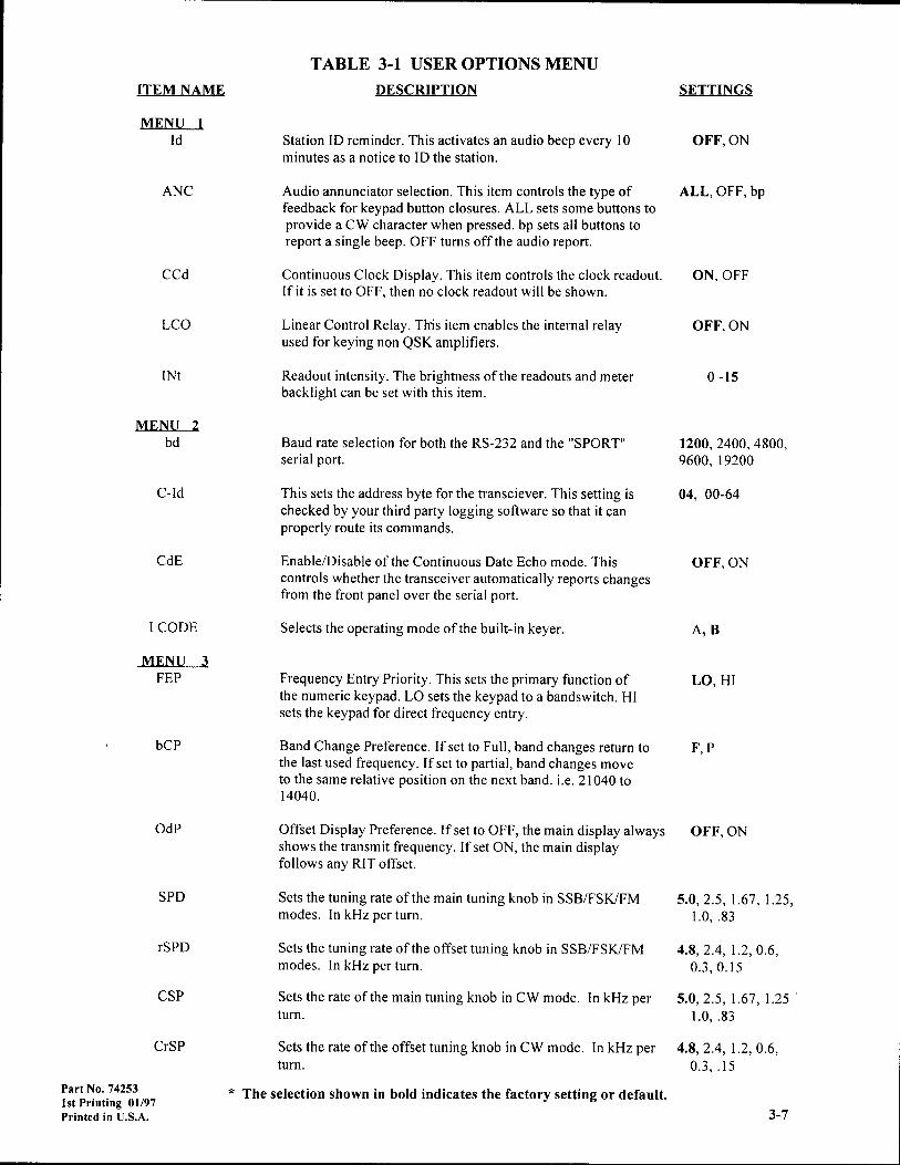
ITEM NAME
MENU IId
ANC
CCd
LCO
INt
MENU 2
bd
C-Id
cdE
I CODE
MENU 3FEP
TABLE 3-I USER OPTIONS MENUDESCRIPTION
Station ID reminder. This activates an audio beep every l0minutes as a notice to ID the station.
Audio annunciator selection. This item controls the type offeedback for keypad button closures. ALL sets some buttons toprovide a CW character when pressed. bp sets all buttons toreport a single beep. OFF turns off the audio report.
Continuous Clock Display. This item controls the clock readout.If it is set to OFF, then no clock readout will be shown.
Linear Control Relay. This item enables the internal relayused for keying non QSK amplifiers.
Readout intensity. The brightness of the readouts and meterbacklight can be set with this item.
Baud rate selection for both the RS-232 and the "SPORT"serial port.
This sets the address byte for the transciever. This setting ischecked by your third party logging software so that it canproperly route its commands.
Enable/Disable of the Continuous Date Echo mode. Thiscontrols whether the transceiver automatically reports changesfrom the front panel over the serial port.
Selects the operating mode of the built-in keyer.
Frequency Entry Priority. This sets the primary function ofthe numeric keypad. LO sets the keypad to a bandswitch. HIsets the keypad for direct frequency entry.
Band Change Preference. Ifset to Full, band changes return tothe last used frequency. Ifset to partial, band changes moveto the same relative position on the next band. i.e. 21040 to14040.
Sets the tuning rate of the main tuning knob in SSB/FSK/FMmodes. In kHz per turn.
Sets the tuning rate of the offset tuning knob in SSB/FSK/FMmodes. In kHz per turn.
Sets the rate of the main tuning knob in CW mode. In kHz perturn.
Sets the rate of the offset tuning knob in CW mode. In kHz perturn.
The selection shown in bold indicates the factory setting or default.
SETTINGS
OFF, ON
ALL, OFF, bP
ON, OFF
OFF, ON
0 -1s
1200, 2400, 4800,9600,19200
04, 00-64
OFF, ON
A'B
LO, HI
5.0,2.5, 1.67 ,
1.0. .83
4.8,2.4,1.2,0.6,0.3, 0.15
5.0,2.5,1.67,1.25L0, .83
4.8,2.4, 1.2,0.6,0.3..15
bCP
CSP
CrSP
Part No. 74253lst Printing 0l/97Printed in U.S.A.
F,P
Offset Display Preference. If set to OFF, the main display always OFF, ONshows the transmit frequency. If set ON, the main displayfollows any RIT offset.

3-4 USER OPTION MENUS The items in
these three hidden menus permit the operator
to tailor the transceiver to match their personal
preference. To access the menus, press and holdthe LOCK button for about 2 seconds. The read-
out will ask "choose", Press either l, 2 or 3 on
the numeric keypad depending on which itemsyou wish to modify. Once a menu has been se-
lected. use the main tuning knob to scrollthrough the items. Use the UP/DOWN Eurow
buttons to modify the status of each item. To
switch to another menu, press the LOCK but-ton once then select the new menu. To exit com-pletely, press LOCK twice.
Refer to Table 3-1 for a list of the items ineach menu and a description of the settings.
3-5.0 OTHERFRONT PANEL CONTROLS(Refer to Figure 3-1).
3-5.01 RF OUTPUT POWER (PWR) Set
METER to FWD (forward power) and turn thiscontrol clockwise for the desired power level,
up to 100 watts output. NOTE: If full clock-wise does not result in 100 watts output, switchthe meter to Ic collector current position and
adjust the PWR control for an Ic not to exceed
20 amps. Read 3-5.02 below for more informa-tion on SWR.
3.5.02 FORWARD AND REFLECTEDPOWER Anytime 100 watts output is notavailable. the most likely cause is SWR in the
2:l range or higher. The transmitter is protectedunder this condition by a current limit that willnot permit it to draw more than 21 amps. The
SWR (reflected power) position on the meterreads SWR directly, on the bottom scale. In case
of high SWR, the cause should be corrected oran antenna tuner should be used.
3-5.03 MIC GAIN ADJUSTMENT WithPTT or VOX activated, speak into your micro-phone at normal operating voice level and ad-just MIC gain control so the ALC light just
3-8
blinks on voice peaks.
3-5.04 SPEECH PROCESSOR USE Press
PROC (processor) switch ON. Switch METERto PROC. Adjust PROCESSOR control untilvoice peaks are in the heavy black line rangejust beyond half scale on the bottom PROC
scale. Now, check the MIC gain setting and re-
adjust, as needed, for ALC light blinks on voicepeaks.
NOTE: The processor meter function is active
even in receive mode. To prevent this frominterferring with the S meter, switch awayfromthe PROC position when it is not being used.
3-5.05 -2OdB RECEIVER ATTENUATORBecause of the outstanding selectivity and us-
able dynamic range of this receiver, you may
never need the ATTN feature. Should you ex-
perience receiver overload, turn the ATTN on.
3-5.06 NOISE BLANKER This noiseblanker is designed for pulse noise such as en-
gine ignition, many commontypes ofpowerlinenoise and noise from some common householdappliances. When such noise is present, simplyadjust the N.B. control for minimum interfer-ence. Always leave the N.B. control in the
maximum counterclockwise position when notin use. This position is off. NOTE: Voicepeaks on a strong SSB signal look like noisepulses to the noise blanker. These peaks will be
blanked if the N.B. control is not in the fullCCW position and the received signal audiomay sound badly distorted.
3.5.07 AUTOMATIC GAIN CONTROL(AGC) ON/OFF The function of AGC is tomaintain a relatively constant audio level overa wide range of received signal strengths. Some
operators will argue that under extreme weaksignal conditions better intelligibility is deliv-ered with the AGC off, the AF gain full clock-wise and using the RF gain control for a vol-
Part No. 74253lst Printing 0l/97Printed in U.S.A.

ume control. Use caution when using this setup,
keep one hand onthe RF gain control. Ifa strong
signal appears nearby, it will be very loud. Themore commonly used setup is the AGC on, RFgain full clockwise and using AF gain for the
volume control. If AGC is off, "S" meter is notactive.
3-5.08 AUTOMATIC GAIN CONTROL,FAST/SLOW This switch selects the decaytime constant of the AGC circuit. As a general
rule, use FAST AGC on key-down modes suchas RTTY, and FM, weak SSB and CW signals.Use SLOW AGC on strong SSB and CW sig-nals. This will minimizethe noise level receivedbetween voice peaks and CW characters.
3-s.09 AUDrO (AF) AND RF GArN CON-TROLS As a general rule, the RF gain controlwill always be set at maximum clockwise anduse the AF control for audio volume level ad-justments. See 3-5.07 AGC ON/OFF above, foralternate methods.
3-5.10 S-METER When the transceiver is inreceive, the RF gain control at the maximumclockwise position, and AGC is ON, the S-meter is functional, regardless of the METERswitch position. Each S-unit is 6 dB. 59 is cali-brated at 50uV.
3-5.11 SQUELCH This control is in the cir-cuit in the FM mode only. Select FM mode, tuneto a clear frequency and adjust the squelch con-trol just into the threshold for receiver quiet-ing.
NOTE: FM operation on the HF bands is pres-ently authorizedfrom 29.0 to 29.7 MHz only.
3-5.12 PASSBAND TUNING (PBT) This isone of the most useful of all ofthe receiver con-trols. It allows you to move the passband backand forth across the desired signal. It can beused to "drop" QRM out of one side or the other
Part No, 74253lst Printing 0l/97Printed in U.S.A.
of the passband or it can simply be used to im-prove the quality and intelligibility of a signal.
Typically the operating position of the controlon SSB and CW will stay between 10:00 and
2:00 and will normally be right at 12:00. Thismay vary depending on which I-F filter is se-
lected. When operating any ofthe digital modes,
such as RTTY, AMTOR or PACKET, the con-
trol position will center at about 3:00. Use PBTto balance the amplitude of the mark and space
signals and to deal with QRM.
3-5.13 USING THE CARRIER NOTCHTwo different notch filters are available for re-
moving interfering carriers. The MANUALnotch is a narrow but deep notch filter that canbe tuned from 200 Hzto 2.5 kHz using the frontpanel NOTCH control. This notch is availableat all times and works well with CW and digi-tal mode signals. When not in use, the NOTCHcontrol should be left fully counter clockwisewhere it will not effect the audio passband.
The AUTOMATIC notch is implementedwith a special digital algorithm in the DSP sys-tem. The NOTCH pushbutton enables this func-tion. There is no frequency adjustment for theautomatic notch, it will seek out and null allconstant carriers in the receiver passband. Thisnotch works well for SSB mode but is not use-ful in CW as it also tends to NOTCH out thedesired signal.
3-5.14 QSK FAST/SLOW This pushbuttoncontrols the quickness of the receive audio re-covery after key up. The fast QSK setting willallow the CW operator to operate "full break-in" up to about 25 words per minute.
QSK SLOW allows the user to select a
slower recover time. This feature is for opera-tors that prefer to keep the receiver muted dur-ing short breaks in their CW transmission. Toset the QSK delay, select CW mode then pressthe DLYbutton. Use the UP/DOWN buttons toselect a setting between 01 and 15. This settingalso controls the hane time of the linear control
3-9

relay in CW mode. QSK can be ovenidden en-
tirely by plugging a hand or foot operated trans-
mit/receive switch into the rear panel MUTEjack.
3-5.15 ANTENNA SWITCH, MAIN/AUX.ILIARY If a traditional transceiver antenna is
connected through the SO-239 coax connector
on the rear panel, select MAIN antenna. If a
separate receive antenna is connected throughthe rearpanel AUX RX ANTENNAphono jack,
select AUX. Both antennas may remain con-nected to the transceiver. They are switched in-ternally for proper isolation.
3-6 REAR PANEL CONNECTIONS (Re-
fer to Figure 3-2).
3'6.01 EXTERNAL SPEAKER This 1/4"jack supplies audio to an external 4-16 ohmspeaker. The level is controlled by front panel
AF control. Built-in speaker is muted when thisjack is used.
3-6.02 INTERFACE PORT This 25 pin "D"connector allows direct RS-232 interface witha personal computer. See Chapter 5 for pin as-
signments. This port is also used to interfacewith TEN-TEC accessories such as the Model420 Solid StateLinearAmplifier. Accessory "Y"and extension cables are available. Use a stan-
dard straight thru serial cable to connect to yourcomputer.
3-6.03 MARXTSPACE Controls the FSK cir-cuit on the digital modes and is typically con-nected to FSK output jack of a modem or ter-minal unit. Logic levels required are less thanor equal to 1.0 Vdc for MARK, equal to orgreater than 2.0 Vdc for SPACE. Either a stan-
dard TTL level or open collector output willdrive this input.
3-6.04 AUDIO IN This input is in parallelwith the front panel MIC connector. Input level
is adjustable by front panel MIC gain control.
3-6.05 AUDIO OUT Fixed level audio out, I
mw @ 600 ohms, intended for accessories such
as phone patch or digital mode equipment.
3-6.06 SERIAL PORT This 1/8" jack allows
2 wire computer control using TTL logic lev-
els.
3-6.07 POWER A four pin connector is the
input forprimary dc power. See Chapter 1, Sec-
tionl-1 for wiring information.
3-6.08 GND Groundpostto be attachedto the
station ground.
3-6.09 TX OUT/TX EN Amplifier controllines foruse with TEN-TEC QSK linears. Mustbe jumpered when not connected through a
TEN-TEC amplifier or the OMNI VI P/zs willnot transmit.
3-6.10 MUTE Input for manual transmit/re-ceive switching such as a hand or foot switchused to over-ride QSK on CW mode.
3-6.11 PTT Use fortransmitter control on any
mode other than CW. This is in parallel withthe PTT connections on front panel MIC con-
nector. Generally used for external systems such
as digital gear.
3-6.12 KEY Connection for an independent,
external, CW key or keyer.
3-6.13 KEYER To connect external paddles
to operate built-in electronic keyer. See Chap-
ter l, Section 1-4 for wiring information.
3-6.14 AUX +13.5 V Any accessory that op-
erates at 13.5 Vdc, less than2 amps, can be pow-ered from this jack. Turn off power before con-necting to or disconnecting from this jack.
Part No. 74253lst Printing 01/97Printed in U.S.A.3-10
3-6.f5 RELAY [N.O.l Used to control non-
QSK amplifier requiring heavy relay switchingcapacity. Delay is adjustable in QSK SLOW. See
Section 3-5.14. To enable this relay which isnormally turned off, see Section 3-4, USER OP-
TroN MENUS (LCO).
NOTE: },OU MUST VERIFY THE AMPLI-FIER KEY INPUT REQUIRES ONLY A LOWVOLTAGE DC CONNECTION TO GROUND.
3-6.16 AUX RX ANTENNA Input for sepa-
rate receive antenna. Selected by front panel an-
tenna switch, AUX position, Antenna may re-
main connected whether or not it is in use.
3-6.17 50 OHM ANTENNA Connection tothe transmitter output and antenna input to the
receiver when a sinsle antenna is used fortransceive.
Part No. 7.1253
lst Printing 0l/97Printed in U.S.A.

II
ru:*rc
t
f-
6r]xtrt
^T:Xsa
P80C
;9
-161"Tgt\t-?Ec
CI|!,||\II VIPL{'S
FIGURE 3-1. MODEL 564 FRONT VIEW
3-12
FIGTJRE 3-2. MODEL 56.I REAR VIEW

IG&
JFr
r$J.i
.')
,f,P&r"I*'-sfI
ry
ffi
Part No. 7{253lst Printing 0l/97Printed in t .S..\. 3-13
FIGURE 3-3. MODEL 56.I TOP VIE\\'

.mMw;ffif#Effist
"vd6 ;{' A{*Ss',. :'di*rr
x*u
3-t-l
Part No. 74253lst Printing 0l/97Printed in U.S.A.
FIGtTRF, 3-.1" rll(|l)[.], 56'l ti(r'{"tOM VI[]W

4.f INTRODUCTION: The following sec-tion contains detailed circuit descriptions andschematics for all of the circuit board subas-semblies used in the OMNI VI Plus. Also in-cluded are outline drawings and photo-graphs that show important components andadjustments.
4-2 DC POWER rNPUT BOARDS (81s91)
This module is located inside the lowpass filter cage at the back of the transceiver.On the rear panel, the DC Power connectorbrings in +13.5 VDC through fuse Fl. Only afast blow style AGC25 should be used here.
On the DC Power Input board, Q2 con-trols the power-on relay Kl. Q2 is biased onthrough the front panel POWER switch at con-nector l. Over voltage protection is providedby Dl and Ql. If the DC voltage exceeds 16volts. transistor Ql will trigger and keep e2from closing the relay. Resistor R5 samples
the current delivered to the l00W RF amplifiermodule. This small voltage drop is cabledthrough connector 5 to the 9 MHz Filter/ALCboard where it is monitored by the ALC cir-cuitry. Connectors 3,4 and 6 distribute +13.5VDC out to the other boards in the transceiver.
FIGURE 4-l: DC
CHAPTER 4
CIRCTTIT DESCRIPTIONS AND ILLUSTRATIONS
r8l
I
ll-=l8t I
t__J, @@t--I
LOGIC EOARO NOW PLUGSTo coNNEcroR @ THrs FEEosUNSIYITCHEO +I55 IOLTS TOTHE XTAL O\€N
REAR PANELCONNECTOR
REFERENCE OESIGNATORS LAS] USEDc3,D2,Ft,x1,02.R5
R247K
RJl.0K
R,t17K
KI
T_ R5r.015 tow
+I2V SSITCHED
+r2v uNswtTcHEoIO LOGIC BOARD
TO RF AUPLIFTER
TO 5.-5.5 PLL 8RD
l-,,lpTf :. UNLESS OTHERTUSE SpECtF|EOr) cAPAcrroRs rN urcnorrnros tr i12) rN_o_ucroRs rr.r urcnoHer.rnvs gI;'3) REslsroRs rN oHMs xsz t/iroit
---lBRo.
i
NOT I
_u:Egl
Part No. 74253lst Printing 0l/97Printed in U.S.A.
DI1N52468r6v Q2
2N4t21
FIGURE 4-2: DC INPUT BOARD SCHEMATIC (Sl59t)
4-l

4-3 LOW PASS FILTER BOARD (81592)
This module contains an anay of six 5pole low pass output filters, the T/R switchingcircuitry, directional coupler for forward powerand SWR detection. and diode switched receive
antenna circuits.Six band lines from the BPF/Front End
board enter at connector 14 where they pass
through rf chokes L6-L11 and energize relaysK2 - K13. These band lines also exit at con-nector 8, where they are routed through the TXAudio board to the 25-pinconnector on the rearpanel of the OMNI VI. Only one of the sixlines is high at any one time based on the oper-ating frequency of the transceiver.
The 100 Watt RF output of the PApasses through one of the selected low pass fil-ters and then through the contacts of relay Kl,which is energized by "T" voltage. The outputpower then proceeds through the primary of theSWR bridge transformer T1 to the rear panelantenna connector. Bridge transformer Tl andassociated circuitry discriminate between for-ward and reflected power to develop drive volt-ages at connector 12 for the ALC and RF me-
tering circuits on the 9 MHz MixerilF board.
On receive, Kl is open and "R" voltage is ei-
ther applied to R24 or M7 through connector7. The front panel mounted ANTenna switchselects R27 for the main receive antenna and
R24 for the AUX receive antenna at connector13. When the Main Antenna is selected "R"voltage is applied through R24 to the emitter ofQl. This turns on Ql and forward bias diodesD6,D7 and D8 thus allowing the signals fromthe Main Antenna connector to pass through tothe receiver front end at connector 17. WithAUX. Antenna selected "R" voltage is passed
through M7 to turn on diodes D4 and D5 al-lowing the auxiliary receive antenna signals topass through to the receiver front end.
During transmit, relay Kl is closed andpasses the filtered PA output to the Main An-tenna connector. A small sample of the trans-mit signal is passed through Cl2 to voltagedoubler Dll - D14. They develop about 150
volts of reverse bias for diode switch D6, Djand D8 to protect these diodes and prevent thetransmitter signal from leaking into the receiverfront end.
Ht-tnmo10vl ll-l I ll ll ll I
f]U:".1]rll - o (-)o
--==H€=EEt[rfEhinrr | !J l-r
- c:f c-:f c-
- E
trtr-@^mEEt-0E0r5nnU f^8 : :-: - :"r-r_uI I =ttZ' FirO Q
lruEEEEEEflNFIGURE 4-3: LOW PASS FILTER BOARD COMPONENT LAYOUT (31592)
Part No. 74253lst Printing 01/97Printed in U,S.A.
K3 K5 K7 K9 Kl1 K13
4-2

lo PA qJT'tJI
6a-crlar .or
t.ro@Lt a20u taoLt !@u0 r@ril t@
ooo- ll u.llr.0 dIt r
uRtsEnl
Part No. 74253lst Printing 0l/97Printed in U.S.A.
NOIE: UNLESS OTHERW|SE SPEC|FIEDl) CAPAOTORS tN UTCROFARAOS (uF)2) TNDUCTORS tN rtCRo{ENR!6 (uH)-J) RE9SToRS rr,t o<ts *5I r/rw
@
na.D
Lttr@
clslOtl c$
ftotl
cJer6tt ct,l.bt
croalsl clt
.JOl
Lt6 l5J:t2-15 .J2 uHLr7 65J,:t2-ta .J2 uHtlE ElLl52-12 .,aJ uHLtg E:Lt:t2-rJ ,,ro vHLzO Es:u2-lO .56 uHL2l 155J2-ll .aJ uH122 65:t52-O8 .6t uHL2J E5J:12-O9 .65 uHL2a t55.ll2-0J 2.5 sH125 ltJJ2-O4 1.6 uH126 E5JJ2-01 J.,l uH127 E5JJ2-02 2.6 uH
Ittoc!|.72a
L. llrcilr ll
02-0J BATitlo.-05 uPNJ700o6-0E lNirOOT09-014 tN4litS0r-02 2N65r9
NOT UStDcr0RE0r
t
tl
tl
ct2l0ti
FIGURE 4-4: LOW PASS FILTER BOARD SCHEMATIC (31592)
4-3

4-4 BPF / FRONT END BOARD (81593)
This module handles the receive func-tions of band pass filtering, RF preamplifier,receive mixer and mixer post amplifier. Trans-
mit functions include transmit mixer, transmitamplifier and band pass filtering.
On receive, the incoming signals enter
at connector 17. Relay Kl, Rl0 and Rl1 make
up the switchable -20 dB attenuator networkcontrolled from the front panel. Following the
attenuator is an AM broadcast high pass filterwhich cuts out everything below about 1.6
MHz. This protects the filter switching diodesfrom large AM broadcast signals. TransformerT8 and capacitor C4, create a tuneable notchfilter which is set to the receiver's IF frequencyof 9 MHz. This network helps improve the IFrejection of the receiver, especially on the 40
meter and 30 meter bands where the desired sig-nals are close in frequency to the 9 MHz IF.
Top coupled band pass filters, one foreach ham band, are selected from connector 86.
These filters protect the front end from unnec-
essary out of band signals and set the IF and
image rejection performance of the receiver.
The grounded gate amplifier stage, Q2-
Q5, provides about 9 dB of gain at a very lownoise figure. It's output feeds the high level
diode mixer D31. LO drive to the mixer is am-
plified by QlO and Ql l The mixer output isterminated through matching transformer T6into another grounded gate stage Q6-Q9. Thispost mixer amplifier is set for about 6 dB gain
and drives the 9 MHz two-pole monolithic fil-ter on the 9 MHz crystal filter board throughconnector 25.
On transmit, the active mixer circuit,Ul, translates the transmit IF signal from con-nector 27 to the desired operating frequency.The mixer output is amplified by Ql and ap-
plied to the band pass filters which remove un-wanted mixer components from the transmitcarrier. Once filtered, the transmit signal is
routed from connector 24 to the Low LevelDriver Board.
t= [J* n I fu== .e#rip'd-EqFa-r
TUoosun'ofrd#"-
EiEiE=E%d,h'd#ffirErErE.F.n,ilH-;E;E-81+:+-F*:F-Fp.--no:E do pc p'o Ee;o Ee;o Fn 81ss3
=g=r?:!:.. dp,-
"tt^'[:[Ptt." $aj:E#g#bH'rtuslln,'ffiqFIGURE 4-5: BPF / FRONT END BOARD COMPONENT LAYOUT (81593)
Part No. 74253lst Printing 0l/97Printed in U.S,A.4-4

l:;l:?!88{{,1!!{!!l:nteE!rq!FeReBr{ra,{s:.{Ftqrlglla{geaoaaldEedsFsFFrt4gE,iEEneleel!615r€EIiE3P
$8e
t
v
It
:rFi !a
??- Ee0o6 00
u{tl!.!cr|{tu|csolulltlBl14lu{t
:*igi*
x
!F!d
Part No. 74253lst Printing 0l/97Printed in U.S.A.
gt Es
FIGURE 4-6: BPF / FRONT END BOARD SCHEMATICS (81593)
4-5

4-5 9 MHz CRYSTAL FILTER BOARD(81782)
The 9 MHz Crystal Filter module inte-grates transmit and receive functions. On re-ceive this board performs the first narrow fil-tering for both FM and SSB/CW. Noise bankersampling and noise gate circuitry are also in-cluded and all the metering circuitry is included.
Receive signals from the Front / End I st
Mixer enter at conneitor 25. Two tuneable net-works match a2pole monolithic filter, Yl, intothe 50 ohm system. This 15 kHz bandwidthfilter protects circuits further down from strongout of band signals. This is especially impor-tant to the operation of the noise blanker andFM detector.
The band limited signals are amplifiedby Ql, which drives buffer stage Q2 and theband pass filter of T2, T3 and C10-C12. Thisfilter adds the slight amount of group delayneeded to get the noise blanker's output pulseahead of the offending noise pulse. The noisegate T4, T5 and diodes D1-D4, can then openin time to prevent noise spikes from reachingthe narrow fiter Y2. This eight pole 2.4 kHzladder filter is the first stage of SSB/CW selec-tivity. Two additional filter positions can beselected with the front panel Nl and N2 but-tons. These optional filters are positioned inseries with the standard filter so that the tworesponses add. A low noise amplifier stage, Q4between the two filters preserves the receivernoise figure and can be set to compensate forthe loss of several different filters.
On transmit, single sideband generationis accomplished by using the standard 9 MHzfilter to strip off one half of the double side-band signal at connector 37. This SSB signal isthen amplified by Q7 and Q8.A voltage con-trolled attenuator, constructed from pin diodesD18 and D19, regulates the level of the trans-mit carrier at the output connector 27.
The control voltase for the attenuator is
derived from the forward power voltage at con-
nector 12. This arrangement provides negativefeedback to hold the peak transmit output powerconstant under changing amounts of micro-phone drive. A separate circuit with U2 and Q14monitors the Final Amplifier current consump-tion. The transmit carrier is cut back if the cur-rent drain exceeds a safe level. This feature gives
the amplifier some tolerance to badly matchedloads.
Alignment
In the receive path there are four tunedcircuits to peak. C3 and C4 optimize the match-ing of monolithic filter Y1. Cl0 and C12 reso-nate the LC bandpass filter. These adjustmentsshould be made using a signal generator and an
audio level meter. Tune in the test signal andadjust each trimmer for peak output.
The transmitter alignment requires a 50ohm dummy load, an accurate rf watt meter anda DC ammeter with 20 to 30 amperes full scale.Hook the ammeter in series with the DC sup-ply to the transceiver. Using the 20M band, keythe transceiver through the watt meter and intothe dummy load. With the front panel RF PWRknob completely clockwise, adjust R46 for 100watts. Set the Meter Switch to FWD and adjustR52 for a 100W indication. Set the meter switchto Ic and note the reading on the DC ammeter.Adjust R57 until the panel meter indicates 2amperes less fhan the DC current measurements.
To set the current limiting, first turnback the RF PWR knob to about the 72 o'clockposition. Now unplug cable #12. Slowly ad-vance the RF PWR control while watching theDC ammeter. Adjust R54 so thatthe transceiverdraws 22 anperes with the RF PWR controlturned fully clockwise. Reconnect cable #72andcheck that the output power returns to about 100watts.
Part No. 74253lst Printing 0l/97Printed in U,S.A.
4-6

b:
}El-
^' ll@a :
Ff?*tEi = ii .-1h;--1 mj a d
-.i R: J'(-) I::i u 6
al6F-
€Q
Fa
Qa
'l
N
t-Iv
p
lFT1
o- 6
p9 ir dd
iQ
rfr
a
ll F--l T\
:R-:
-.ll-+
1H,
.1t-*
^^--F
1T\
i;o
Part No. 74253lst Printing 0l/97Printed in U.S.A. 4-7

4-6 PASS BAND TUNING BOARD (81781)
The Pass Band Tuning module enablesthe operator to position a crystal filter passbandrelative to incoming receive signals. By adjust-ing the front panel PBT control, the receiverband width can be manipulated to reject inter-ference. The standard2.4kHz 8 pole or one ofthree optional filters can be selected with theBandwidth buttons above the main tuning knob.
Noiseless feedback amplifier Ql takesreceive signals from the 9 MHz filter board atconnector 38. This stage feeds the diode ringmixer D1-D4. L.O. for the mixer comes fromthe 15.3 MHz voltage controlled crystal oscil-lator Q4. The mixer translates the 9 MHz inputsignal down to the 6.3 MHz passband of thecrystal f,rlters. The exact position of the receivesignals relative to the crystal filter is set by thevoltage on varactor D5. Two alignment stepsset the tuning range to +\- 1.5 kHz.
One of the four filters is selected by theLogic board through connector 4l . Each filter
is preceded by a resistor pad to equalize the sig-nal loss regardless of bandwidth and three pindiodes at each position help maintain the 90 dBultimate rejection. Following the filters is thesecond mixer stage Q9. The dual gate MOSFETtranslates the receive signals back up to 9 MHzfor the IF/AF board. Three tuned circuits withL17, Ll9 and L2l peak the response of themixer.
Alignment
To set the tuning of the voltage con-trolled crystal oscillator, hook a frequencycounter to the test point adjacent to the coaxjumper cable. With the front panel PBT knobfully clockwise, adjust C24 for 15.3015 MHz.Now with the PBT knob centered, adjust Rl8for a reading of 15.300 MHz.
To peak the three adjustable coils, tunein a test signal and watch either the S-meter oruse an audio level meter to adjust the output formaximum.
STRNDRRD
2.1 kHz
0
-000
E
{0
E
{0
o lo
rlooEL 2A8
1.8 kHz
e Ie
HODEL 285
O.5O kHz
o o
|1oDEL 282
Q.25 kHz
+OF Er--l
e)v
o:=oI e-<=
r:BnD'{ul-og:'rH',tr
t_l c)Lr Fl o
[oEo
ffiiqrytTal-,voE
-=FP\)E
-rSil
s*p;?g)E/[0of$zr L
E
].
uu
oI
Q103 Fo=t-t (
[,;
9roE
@ilo@,
Part No. 74253lst Printing 01i97Printed in U.S.A.
4-8
FIGURE 4-9: PBT BOARD COMPONENT LAYOUT (81781)

fl1HI
Iq
^FiETs3iB9i5==i
;!J -J39-
t.^tief;*IF?Fb
=odots'
q3's6dd88
e 393e
:s I si' !€
a=:
EEI
!rr
frat;
iffil^i* a$
c
6
Ei,3s5 - 6\iii R \o/o6a --d!
Part No. 74253lst Printing 01/97Printed in LI.S.A.
tnFt toFl
lEil lsillerl leil
FIGURE 4-10: PASS BAND TUNING BOARD SCHEMATIC (81781)
4-9

4-7 rF/AF BOARD (81602)
The IF/AF module consists of threestages of IF gain, the AGC system, product de-
tector and the audio circuitry.Receiver IF signals from the Pass Band
Tuning board enter at connector 43. Groundedgate JFET Ql forms the first amplifier stage.
The AGC voltage fed back to Q2 controls PINattenuator diode Dl which limits the peak - to -peak signal level at the input of U1. Integratedcircuit IF amplifiers Ul and U2 contribute mostof the gain in the entire receiver. These twoamplifiers are also controlled by the AGC volrage. Q3 buffers the output of the last amplifierand drives the product detector U3 and the AGCrectifiers D6 and D7. The AGC constants are
set by R2l, C30, R22 and C 27. The AGCFAST/SLOWOFF switch connects at terminal49.
The product detector U3 mixes the IFsignal with the BFO from connector 46. Theaudio output at pin 6 is then filtered and ap-
plied to a switched capacitor notch filter U5.The notch frequency is determined by the clockrate from VCO chip U6. This is set by the con-trol voltage from the front panel NOTCH knobat connector 53.
Analog switch U7A and U7C form a
SPDT switch under the control of the Losic
board. Audio from either the FM detector at
connector U or the notch filter is selected and
routed to the DSP interface chip through con-
nector 54. Processed audio from the DSP cir-cuitry then returns at connector 56.
The volume is set by the front panel AFGAIN knob at connector 55. A separate path
around the AF GAIN control is provided byU7B. This switch is used to make the CWsidetone independent of the knob setting. Au-dio amplifier U8 provides up to 1.5 Watts toeither the internal or an external speaket.
AlisnmentAdjustable coils L3 and L5 peakthe gain
of the two IF amplifrers. Use either a steady offthe air CW carrier or a signal generator and peak
the S-Meter reading.S-Meter alignment should be performed
only after all the other receiver adjustmentshave been made, and will require a calibratedamplitude signal source.
Two trimmers, R29 and R25, adjusts the
S-Meter offset and full scale. Start with a 50
uV signal into the antenna jack and adjust R25for an 59 meter indication. Next lower the in-put to 1.60 uV and adjust R19 to read 53. Re-peat these two steps several times until there isno interaction.
hvz0/\-ooE
I
4-10
Part No. 74253lst Printing 0l/97Printed in U.S.A.
FIGURE 4-11: IF/AF BOARD COMPONENT LAYOUT (81602)

9;Hir{
oo:U!.rt6
8s
$e
!a:
36 3g+---1
:E
@EE
iau'
rXcr
cJaf
Ax
gE ..8qi Egfis9c$t3t! 3s3of
i33EE53
g$i
$i$fi
Ei:n
eEqt
oaoI
.U
HE3$::
F@E|'|!'EA
- nldoa6
oo-ooo
mI
sio
F(-)o
oT6(
IrStl- do
I
€
Part No. 74253lst Printing 0l/97Printed in U,S.A.
*-ijFrF
Eet gFh
tL-----J
FIGURE 4-12: lF I AF' BOARD SCHEMATIC (S1602)
4-tl
_J

4-8 s.0 - s.ss MHz PLL BOARD (81s99)
The phase noise characteristics of the
OMNI VI depend entirely on the design of the
5.0 - 5.5 MHz synthesizer. The synthesizer is
actually a two loop system that operates at 200
ti220 MHz and tunes in 400H2 steps. Its out-put is then divided by 40 to produce the desired
5.0 to 5.5 MHz output. This division by 40 notonly reduces the output frequency but also re-duces the phase noise and spurious levels by afactor of 32 dB.
The synthesizet's l0 Hz tuning resolu-tion is derived from a voltage controlled crys-tal oscillator (VXCO) Yl, Q2. Digital informa-tion from the microprocessor is clocked in seri-ally t connector 87 and loads the shift registerchip U3. The 8 bit output of U3 is applied to an
R-2R resistor network, R23, which is used toprovide digital-to-analo g conversion of the out-puts of U3. U4A and U4B buffer the analogoutput from the resistor network and providegain and offset adjustments (R27 and R3l) toalign the frequency of VCXO.
The VCXO output from Q2 is doubledby T2, D1 and D2, and then heavily filteredbefore it drives the diode mixer in the feedback
path of the main loop. The mixer D3-D6 sub-
tracts the VCXO frequency from the main loop's
output which has been buffered by Q4. Thisdifference signal becomes the feedback for the
main loop. Q3 is a filtered amplifier stage whichboosts the mixer output to a level sufficient todrive the prescaler chip U5. Since the loopworks to keep this feedback signal constant infrequency, the small steps from the VCXO are
imposed onto the main loop output.Reference and divide-by-N dividers in
PLL chip U6 are programmed serially from themicroprocessor through connector 87. The 10.0
MHz reference signal applied to connector 88
is divided internally in U6 by 1000 to generate
a l0 kHz step size. Phase errors from the PLL'sphase detector steer the charge pump circuit Q6-Q9. The VCO control voltage from the chargepump is low pass filtered and biases varicapdiodes D9 and Dl0. The VCO output is appliedto a two way splitter comprised of T5 and R49,and drives both the mixer buffer stage Q4 andthe high speed divide-by-ten chip U7. The out-put of U7, a square wave of 20-22MHz, clocksa divide-by-four circuit in U8. The 5.0 to 5.5
MHz signal from U8 is then filtered to removeharmonics and exits to the LO mixer board.
E"rFffifis##H-rfl!:tr.fuEr * rEE!l-l-l
-r-r n l-1
frr'F;l'.9r-1
trl-Qnlil
o fr-l
L!FIGURE 4-13: 5.0 - 5.5 MHZ PLL BOARD COMPONENT LAYOUT (81599)
ffi
Part No. 74253lst Printing 01/97Printed in U.S.A.
4-t2

it3:H86i
o??
sat
B5
-N4aOOFO:>>fffff
l,itiiiiEffi9:aa
qfin;il888
a83itS
Part No. 74253lst Printing 01/97Printed in U.S.A.
FIGURE 4-14: 5.0 - s.s MHZ PLL BOARD SCHEMATIC (31599)
4-13

OMNI-VII
Find out what they found out about the new Ten-Tec Omni-VII. Nothing in its price category matches it for receiver performance, ease of use, remote control capability or features! Contact us for complete information today – or see the Omni-VII demo video at www.tentec.com
“My Dad, KB2LAU, in Florida has become active again using my Omni-VII in
Vermont. He is enjoying daily contacts [via Internet remote control]. Being a ham with limited to no antenna options, this has been
a great opportunity.” – W1ZN
“As an avid CW operator, it is like listening to your favorite music
while operating.” – N1SW
“I can say that in my 30+ years of operating I’ve never enjoyed a rig more than the
Omni-VII. The audio is superb as is the QSK, ergo-nomics, receiver characteristics and
on and on.” – W7TEA
“In 40+ years and many receivers, the Omni-VII is the most sensitive,
most QRM proof and most pleasant to operate I have enjoyed. The noise blanker and noise reduction
systems really help me in dealing my sometimes noisy location.”
– K6LE
“Once again, Ten-Tec has produced a superb transceiver, with great SSB audio and their
famous QSK.” – K4SQR
“Close-in dynamic range unsurpassed by any other general coverage
radio.” – Radio Society of Great Britain RadCom review, September 2007
“I was struck by how clean, natural and quiet the receiver sounded in
comparison to some DSP based radios. I found the Omni-VII a real pleasure to listen to –
in any mode.” – W1ZR, in the ARRL Product Review, QST July 2007 “What a neat little package!
I’m having more fun with this thing!” – K1SA
“High quality manufacturing…overall
a very impressive transceiver” – W9AC
Are you next?
1185 Dolly Parton Pkwy., Sevierville, TN 37862 Sales: 800-833-7373 We accept Visa, MC, American Express and Discover. Office (865) 453-7172. FAX (865) 428-4483.Sales: Mon-Fri 8:00-5:30 Eastern [email protected]. Service: Mon-Fri 8:00-5:00 Eastern [email protected] (865) 428-0364.

4-9 XTAL OSC. - L.O. MIXER BOARD(81s9s)
This module generates the main local
oscillator signal which is applied to the trans-
mit and receive mixers in the front end. Band
switching information from the Logic board
enters via connectors 82 and 83. One of the ten
crystals is pin diode switched into oscillatorstage Ql. Buffer stage Q2 drives one side ofthe LO mixer through a low pass filter and also
drives the oscillator level detector D25, Q3.Transistor Q3 sets the bias point of the oscilla-tor stage to stabilize the oscillator output leveland to limit the drive in the crystals for better
aging. Part of the crystal oscillator signal is fed
through buffer transistor Q9 to the Logic board
via connector 84. A PLL circuit on the Logic
board compares this signal to a precision refer-
ence frequency and sends a d.c. correction volt-age back to the oscillator via connector 84,
through R26, R20 to varactor diode D26. This
ensures that the crystal oscillator is always
locked to a precision reference for improved
frequency stability and accuracy.
The synthesized 5.0 to 5.5 MHz signal
at connector 85 is mixed with the crystal oscil-lator signal by active mixer Ul. The desired
mixer product id filtered by one of five band
pass filters and then amplified by transistors Q6,
Q7 and Q8. The L.O. output is then taken offthrough agMHztrap, T5 and C63, which helps
eliminate undesired products from the mixerwhich could leak into the receiver IF.
:" T:*r r oou,:, t,'rt,'r|,+ul,ru,un,ru,rl,ll _l
I'bJ"r*iX.HHHHHHHtrutr |
i ff:=,' ua n:g;'=l'['f"!;il " IlgEo_= _E_81595 ; 6_6-'BLbr I
, O0^H t- --
EEt EE E^ o= (
i?9 -r'E'E'fi"fllo-- -^f o o ?n,.u I
i"eF'-"ggg s'l$ffilT,d- r,a r7r rfi -: oF biQ'pi-nrim r: I
+ lt'rj li l_?l g, ; lu:.^^ tn dtq O,I l--urln :?o' :r-r' :r; r. 6g I'Oo0 ll | " ^"dnY t
, -E _' _=_ =_ =_ | 2 I oo l" qc ln-r--, .^tla[lrsilro= E E E'?i'
Yo_@_ Eo_s'_n i I _ _ "
-_=;"_i
| 6 IJU-o
= :s'9!.rq00 :- o\-/
r
FTGURE 4-15 XTAL OSC. - L.O. MIXER BOARD COMPONENT LAYOUT (81595)
4-t4
Part No, 74253lst Printing 01/97Printed in U.S.A.

irrii iiiitt3ifl3flaflgii!FiiFFitr;tltrtatrta!r rl t 9r! rsF
!tggefr6rese
iiii:ai!oss
agdeS's=s
da
::l:gi:
E6ts ??JIR PPFg
lffi9:aa
i*T
Part No. 74253lst Printing 0l/97Printed in U.S.A.
s.:. 3;
3
Ei!
ti3
f! [e E-q !e
FIGURE 4-16 XTAL OSC. - L.O. MIXER BOARD SCHEMATIC (81595)
4-15

4-10 CONTROL BOARD (81s96)
Based on inputs from the Logic board,
rear panel jacks and front panel switches, this
module develops the control voltages that power
various stages throughout the transceiver. This
board also features an adjustable wave shaping
circuit that sets the rise and fall times of the
transmitted CW envelope.The main mode information from the
Logic board enters at connector 59. Diode and
transistor switching circuits combine these
mode lines with "T" voltage (indicating a key-down) to manipulate the BFO frequencythrough connector 60.
A request to key the transmitter is gen-
erated by grounding either the rear panel or micconnector PTT lines, or the rear panel CWKEY. Any of these inputs will turn on transis-
tor Q9 which sends a transmit request signal to
the Logic board via connector 66. The micro-processor calculates the transmit frequencybased on RIT, CW offset, etc. and reprograms
the phase lock loop. After a short delay of about
10 milliseconds, the Logic board generates a
transmit acknowledge voltage at connector 63.
This signal becomes the external keying loop
that is normally jumpered on the rear panel. Ifan external amplifier is to be used, it can be
included within the keying loop so that the
amplifier can control the timing of the keyingand prevent hot switching.
A separate MUTE, inPut on the rear
panel can be used to mute the receiver and key
the linear relay if it is enabled in the user menu.
No transmitter output is generated however untileither the KEY or PTT lines are grounded. This
method is generally used with non-QSK am-
plifiers.The rise and fall times of the CW rf en-
velope are controlled by the integrator circuitof Q12-Q15. Resistor R24 sets the slope of the
"TD" signal which is used to bias the double
balanced mixer on the TX audio board. This
adjustment will set the transmitter rise time be-
tween about 2 and 4 milliseconds.
EoEoEoEo-E
+ffi:Fde'Wssssss !s str l-r E@ oD Fl l"E"'q!{,ruHWffiTfiF
iJ:s ffi
Part No. 74253lst Printing 0l/97Printed in U.S.A.4-16
FIGURE 4-17: CONTROL BOARD COMPONENT LAYOUT (81596)

o,o6rE+66gl
63i;;--:r
rr@E.
o
ulclEIJI;l
:l
?l:lFI
8t:lEI
;l3l
<taltlolJl
lJUc+Fd
loool
ltlo
rTaloool
ni9gPr+ +
loool
Ue,ets +
toool
3r ii9 h{t€
,^'v'l3u
A9'C I +
A3r
lld
3l nn
N3 Xt
lno xl
)3v xr0d 3rnH
0d x.t
r-to
ua 6o\s/ rfi
@
@a
E:
o
cl
)oFt0LO
+ JIHlrd
93d+lv'13u
x0AhlJ
)sr8S"l8SnA3
3Nnr
rlE;
Ergi9:ea
FFEFE€U YO-u6daq6,J]+FL'U
Part No. 74253lst Printing 0l/97Printed in U.S.A.
Pi Es
FIGURE 4-18: CONTROL BOARD SCHEMATIC (81596)
4-17

4-11 LOGrC BOARD (81606)
This module integrates the LOGIC<DSP and CRYSTAL LOCKING subsystems
onto a single pc board. An 80C32 micropro-cessor (UI) operating at 20MHz, a 32k EPROM(U4) and 8K of battery backed RAM (U5) fromthe core of the logic system. The 80C32 pro-cessor is a member of the 80C51 family of pro-cessors and contains 256 bytes of on-chip ram,
two l6 bit counter/timers, full duplex serial in-terface and multiple interrupt capability. A74HC573 latch (U2) performs and address
demultiplexing and a74HCl38 (U3) provides
address decoding for the bus-oriented periph-
erals. In addition to the EPROM (ROM space
$0000-$7FFF) and RAM chip (RAM space
$4000-$5FFF), the logic system core also in-cludes a real time clock (U6 RAM space
$E000), an Analog to Digital converter (U7RAM space $2000) and 82C55 I/O expander(U20 RAM space $000). The DSP subsystem
is memory mapped into the microprocessorRAM space at address $,4.000 and the OptionalVoice Board is memory mapped to $C000. Alsoincluded on the Logic board are a serially pro-grammed 32bithigh current driver (U22) whichprovides bands switching signals for the trans-ceiver and controls the front-panel keypad in-dicators. The DSP subsystem is comprised ofintegrated circuits u8, u9, u10, u11, u16 and
U23. The DSP subsystem is based on the ANA-LOG DEVICES ADSP 2105 DSP PROCES-SOR with a cycle time of 100 nanoseconds. A27C64 EPROM (U9) contains the DSP programwhich is loaded into the 2105's internal ramduring system power-up. A serial CODEC(U11) provides the Analog to Digital and Digi-tal to Analog functions of the DSP system andanti-alias filtering with a pass band of 200 Hz -3400 Hz. U23 and transistor Ql3, and diodesD4, D5 providethe 5V requiredby the CODEC.Receiver audio reaches the DSP sub-system viacoax connector 54 and exits the DSP sub-sys-tem via connector 56. The DSP processor RE,-
SET line, is connected to the main micropro-
4-18
cessor viaU2} which allows the microproces-
sor to perform DSP sub-system reset duringpower-up.
IC Ul6, a7400 NAND GATE and ICU8, an 8 bit LATCH provides the interface to
the DSP PROCESSOR bus with the Main mi-croprocessor bus. The interface provides a one-
way (MICROPROCESSOR to DSP) interface.
The write signal from the microprocessor also
provides an interrupt to the DSP processor toinform the DSP subsystem that anew commandhas been received.
IC's Ul7, Ul8, Ul9 are used to inter-face the MAIN. REMOTE and OFFSET encod-
ers to the Microprocessor. Ul9 is used to en-
sure smooth operation of the offset encoder bycleaning-up the encoder pulses before theyreach the microprocessor. IC's U l7 and U 1 8 inconjunction with resistor R30, R3l, capacitors
C25, C26 and diodes D2, D3 operate to pro-vide an interrupt pulse for each phase changegenerated by the encoders. When the micropro-cessor receives this interrupt request signal, the
software tuning routines analyze the encoder
signals to determine which encoder is movingand in which direction by reading the encoderpositions via the 82C55IlO expander. IC U21interfaced viaU20 to the microprocessor, pro-vides the keyboard scan for reading keypad sta-
tus. Serial interface circuitry based on U14 andTRANS??? provides level Q18-Q1 I translationfor RS-232 and TTL levels via connectors J2
and 69. Transistors Q1 and Q2 form a2}MHzoscillator which provides the 20 MHz proces-
sor clock and after dividing down the 5 MHzclock to the DSP CODEC. Ul3, a serially pro-grammed PLL IC provides the Crystal Lock-ing control. A sample ofthe selected Band crys-tal is fed to the PLL via connector 84, an errorsignal is generated by the PLL chip and the crys-tal frequency is adjusted as necessary via the
charge pump circuit which feeds a DC correc-tion voltage back over the RF sampling line. Avaractor diode located on the crystal board pro-vides the necessary crystal adjustments.
Part No. 74253lst Printing 01/97Printed in U.S.A.

g-gt]ffiru,,]Oqrrr
ffinOPTIONRL UOICE BORRD
g
urz \ \.y rc,,l
F,.,, Hi1oo
<!;;ffThlsu?l @[
1J0Ud3 dso6n
F--utq_l
nIFUBI
C
816A6 LOGIC
azn
BORRD
l-m--!
!t@
nt@
U5LOGIC EPRON
U5
fll EIEu@!@_@ F-- u21-_l En
-f
r:@ oI
I'arl No. 7125Jlsl Prinling (ll197I'rinted in I l.S.A. .t-t9
ffftrTl= lnXbI TfrtrLJ
=O@5?Tffim. =HFffis,TN
9n
@-Rd'.
FIGURB 4-19: LOGIC B0ARD coMpoNENT LAyour (s1606)

III
II
lc?8 lII ro.,fl
lc?31I
lc:nP36 IOK
{
H@
@ el"
(REFL T!N! CLOCK)
ct? ot
P?e;
v !1,33/ tgv
ct I
ct?
80l,ltc3l
220Rl I
sPfECr Mlo
OPTIONRL UOICE BORRDtmxR37
aatx
l-t nogt-2 AOIt -3 AO2
rr:;: lEFErdrF::35:::3;3srssess
r ot
Frs
RDSP 2lA5 ';;lPO2 xC
Urg Nc
xcI _xC
q6ocooarooo6:i;;33N1!H
3!"ocooooo
"'6riiii:633
4-20
FIGUttE 4-20: LOGIC BOARD SCHEMATIC (81606)

OPTIONRL UOICE BORRO
R?0 9 qT.Llrrt$
-NF DFNT
q077Boo
Foo.DNO<O6666666666o
t saa*I oRIoo Rts
RDSP 2tO5 ';;ltpoa Nc5€r NC
ql llo NC
i:iiFEHg*
.eo NfJ--
d{Fsserssss{clJ,II
ul m32u ?{Hc6736 ?1rc1Sw 27C256r.6 626tLL6 ost2a€u7 6Ea8{8€ ?qc5?3u9 2rc6aaut0 rcsP2r06ult TLc320tlul2 ?4AC74ul3 trl4st70uti mx2turs ?rHc@ul€ ?{rcoul7 ts??aul0 to??Bur9 togsu0 mcs*u2t TtHclSi
0r.02, e8,09 zltoto.ot l 2t403.0t,012_cl3 2tsa8?
zt,t2.za a N23 6&
8i
Es?3i
Lnsr uso Eslmtmsc36, i76,06, Zt, Y2, !1, Ct3!22
l'art No. 7'1253lsl Printing 0l/97PIintc(l irr U.S.A.
Grc lloARD SCHEMATIC (81606)

4-r2LED DTSPLAY BOARD (81s87)
This module contains three groups of7-segment LED displays. Also on this moduleis an array of 4 LED's used to annunciate vari-ous display modes currently in use.
Frequency information is displayed onDSPI through DSP4. These LED's are .56"high, common cathode displays driven by mul-tiplexed segment and digit signals fromthe LED
Display Driver board via connector strip Pl.This connector also provides drive signal forthe annunciator LEDI through LED4.
Offset, time, and memory channel in-formation is displayed on two groups of smaller.3" high LEDs consisting of DSP5 throughDSP12. Multiplexed drive signals from the LEDDisplay Driver board are connected to thesedisplays via connector strip P2.
l-uro nQuro eQselrrQ
uoxQ
L il81587 LED DISPLRY BORRD
FIGURE 4-2rz LED DISPLAY BOARD coMpoNENT LAyour (81s87)
SEGMENTLEGEND
"lI!"
DSPI-OSPJt sP4osP5-0sPEosPo- osPl 2
HosP-572JHDSP-56OJHDSP- 74OJHosP-7l()4
aurP- 184{tHUTP- I 600
lror-LED2I.EOJ-LED4
Part No. 74253lst Printing 01/97Printed in tl.S.A. 4-21
FIGURE 4-22: LED DISPLAY BOARD SCHEMATIC (8lsS7)

rc n_l
r--iez-lll I
FIGURE 4-232 LF,D DISPLAY DRIVER BD. COMPONENT LAYOUT (81588)
lfficq66|ElI oEsr I
ftgffiGdprt4&ErgI5(r't)ffi.98!Grrt$6rrErr/{
Part l.,lo. 74253lst Printing 0l/97Printed in U.S.A.
4-13 LED DISPLAY DRIVER BOARD(81s88)
This module contains two intelligentLED display driver chips, ICI and IC2. Dis-
play data from the Logic board is clocked in
serially to ICI via connector 90. The LOADline is initially set low, then each driver chip
receives 16 bits of serial data. Since the chip's
data lines are cascaded (DOUT of IC1 goes into
DIN of IC2), a continuous string of 32 bits isclocked into DIN of ICl. The LOAD line is then
pulsed high to latch the data in the driver chips
Each chip contains its own internally generated
multiplex clock and LED driving circuits. ICIcontrols the larger .6" high frequency readout
andthe four small LED annunciators, while IC2
controls the two smaller groups of .3" high LED
displays used to display offset, time and
memory information. Display brightness is user
selectable and controlled by commands from
the Logic board. Digit drive signal DG7 from
IC1 is routed via connector 89 to the Low Level
DriverA{.B. board where it is used to adjust the
brightness of the meter lamp.
r;@ 81588 n,F
LED bili'{lto
rflu
IIC1
ll
€isItotr82ataa
6t8aB58CalI
bo
e3aq
8la28Ji_c
4-22
FIGURE 4-23zLED DISPLAY DRIVER BOARD SCHEMATIC (8rs88)

4-14 TX AUDIO BOARD (8rs97)
This module contains the transmit au-dio amplifiers, speech processor, 9 MHz BFOand balanced modulator. It is located at the leftrear of the chassis, on top of the chassis deckbehind the PLL shield box. There are boardmounted connectors for AUDIO IN. AUDIOOUT. MARK/SPACE. SERIAL PORT andINTERFACE PORT accessible through the rearpanel.
Microphone audio from connector 73 ortransmit audio from the rear panel AUDIO INjack is amplified by U2A. The output of U2Asplits three ways to drive the anode of diodeswitch D2l, the speech PROCESSOR controlpot. at connector 74, and the VOX amplifierU3A. Diode D2l is normally forward biasedthrough connector 70 when the PROCESSORswitch on the Lower Pot. board is in the OFFposition, connecting the amplified audio signalto the MIC gain control at connector 71.' The speech processor input at connec-tor 74 is amplified to a nominal 1.2 Volts peakby UIA and again by UlB to approximately1.8 Volts peak. One output of UIB drives rec-tifier D l4 and compressor transistor e I 3. e l3clamps part of the original input to ground ef-fectively maintaining a constant audio level atthe output of UlA. Another output of UIBdrives the processor level meter through emit-ter follower Ql2 and connector 78.
Half the output of UIA appears acrossclipper diodes D18 and D19, but no clippingoccurs at the normal level of 0.6 Volts. The clip-per diodes limit fast audio transients, for whichthe compressor circuit is less effective, to 0.65-0.7 Volts. The compressed and limited speechprocessor output level is set by R65, and U2Bbuffers the output to the anode of diode switchD20. When the PROCessor switch is in the ONposition, D2l is reverse biased, D20 is forwardbiased. and processed audio is passed to theMIC gain control via connector 71. R65 is ad-justed so that the peak levels ofthe processed
Part No. 7,1253
lst Printing 0l/97Printed in U.S.A.
and the unprocessed audio signals at connector7l remain equal as the PROCESSOR switch istoggled between OFF and ON.
The output of the MIC gain control atthe center pin of connector 71 is fed to the bal-anced modulator U4. The balanced modulatormixes the transmit audio signal with the BFOcarrier to produce a 9 MHz double sidebandsuppressed carrier output. U4 is enabled on pin7 by "TD" voltage from the Control board con-nector 60. The balanced modulator gain is in-creased in SSB mode by grounding bypass net-work C4 - R10 through Ql. Q2 unbalances themodulator in CW and FSK modes. Tuned trans-former T1 performs the match to the 20 OhmDSB input of the 9MHzMixer/IF board at con-nector 37. R3 and R4 trim the AC and DC bal-ance of U4 for maximum carrier null.
Part of the transmit audio signal is fedthrough VOX amplifier U3A and emitter fol-lower Ql I and appears at connector 68. Like-wise, a portion of the speaker audio is fedthrough amplifier U3B and emitter followerQ10 to connector 68. These two signals (VOXand ANTI VOX) are sent to the Logic boardfor processing by the DSP circuits, which pro-vide a software controlled VOX system.
The BFO oscillator/amplifier is formedby transistor Q6-Q8, and its frequency of op-eration is determined by crystals Yl-Y2, diodeswitches D8-D12, and capacitors C10-C13,Cl6, C18. Based on the mode of operation, tran-sistor switches Q3-Q5. Q9 drive the diodeswhich select trimmer capacitors to set the BFOfrequency at the proper place with respect tothe IF filter response. Mode information fromthe Control board enters at connector 60. Thetrimmers can be set with a high resolutioncounter at connector 46 by switching modes inthe order listed below and adjusting the corre-sponding trimmer for the frequency indicated:
CW transmit or TUNE, adjust C 10 for 9.000400MHz.
4-23
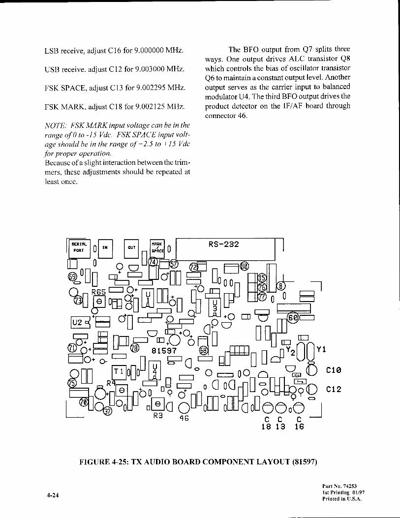
LSB receive, adjust Cl6 for 9.000000 MHz.
USB receive. adjust Cl2 for 9.003000 MHz.
FSK SPACE, adjust C13 for 9.002295 MHz.
FSK MARK, adjust Cl8 fbr 9.002125 MHz.
NOTE: FSK MARK input voltage can be in the
range of 0 to -l5 Vdc. FSK SPACE input volt-age should be in the range of +2.5 to +15 Vdc
for proper operation.Because of a slight interaction between the trim-mers, these adjustments should be repeated at
least once,
The BFO output from Q7 sPlits three
ways. One output drives ALC transistor Q8which controls the bias of oscillator transistor
Q6 to maintain a constant output level. Anotheroutput serves as the carrier input to balanced
modulator U4. The third BFO output drives the
product detector on the IF/AF board through
connector 46.
c1a
ct2
OOoOcc c18 13 16
R3 16
Part No, 74253lst Printing 0l/97Printed in U.S.A.
4-24
FIGURE -ZSzTXAUDIO BOARD COMPONENT LAYOUT (81s97)

lIriisi; 3 I I rE I'r f,@l- tr@ffi' Eo
Ir
i!lt;
RO
!r
!Ill
E, ,,
i til iiiI
E! ii !! ,..
!lu(
Ir-{Flr!
ffi!ffi
;;!!iii
4-25
Part No. 74253lst Printing 0l/97Printed in U.S.A.
FIGURE 4-262 TX AUDIO BOARD SCHEMATIC (81597)

4-I5 LOW LEVEL DRIVER / N.B. BOARD(81608)
This module contains the low level wide
band amplifier for the transmitter, the receiver
noise blanker. "T" and "R" voltage generator
and the "+REG" and meter lamp regulators. Itis located on the left upper chassis on top of the
PLL shield.The operating frequency transmit sig-
nal from the BPF/Front End board enters on
connector 24,is amplified by class A amplifiertransistors Q9 and Ql0, and exits to the FinalPower Amplifier at connector 79. During trans-
mit. "T" voltage supplies bias to both stages
through Rl8 and R21."T" and "R" voltages are developed by
Ql-Q8 based on the level of the "TD" pin fromControl board connector 62.In transmit "TD"is high and Q5 sources approximately 12.5Voltsto the "T" line through R7. while Q7 holds the
"R" line low. In receive "TD" is low and Q8sources approximately 8.5 Volts to the "R" linethrough Rl3, while Q4 holds the "T" line low.
At connector 31, a Sample ofthe 9 MHzreceive IF signal from the 9 MIIz Mixer/lFboard is input to noise blanker amplifiers Uland U2. The output of U2 is split two ways.
Part of the signal is fed through C3l to Q13which provides AGC control of U2. This helps
to maintain a constant output level from U2when there is no noise present or when the
noise pulse widths are long. The N.B. pot., lo-
cated on the Upper Pot. board, controls the
emitter voltage of Ql1 through connector 67.
The output of Q11 is summed with the AGC
voltage from Q12 and sets the noise threshold
of the noise blanker system. The other output
of IJ2 foes to pulse amplifiers Qi4 and Ql5whose output appears at connector 32. This out-
put signal consists of noise pulse components
with fast rise and fall times. which are applied
to a noise gate circuit on the 9 MHz Mixer/IFboard to blank the receiver during noise pulse
intervals. A regulator composed ofUl and Q19 supplies +8.5 Volts "+REG" volt-age to all boards via connector 62 and the Con-
trol board. Ql1 is mounted on the PLL shieldplate and connected with cable Q.
Meter lamp control transistor Q18 islikewise mounted to the PLL shield and con-nected with cable P.. Digit driving pulses are
applied to connector 89 from the LED displayDriver board. These pulses are amplified and
buffered by U3B. integrated by capacitor C18
and applied to regulator control amplifrer U3A.Output of U3A drives Q18 whose output goes
to the meter lamps via connector O. The dutycycle ofthe pulses at connector 89 can be var-ied under software control using the DIM func-tion on the front panel keypad. As this pulse
width is varied from minimum to maximum,the meter lamp voltage varies from about +2.7
volts up to a maximum of about+5.7 Volts.
Part No. 74253lst Printing 0l/97Printed in tl.S.A.4-26

I ol]Dfl,_,_o o o ,-_, ,_o o Qgo3ea'Aifu;HISn'H'{Hr6ol+5fri2\FnoJ'kr* ,l-!;:b"(J- H-=[[- _Er JLq^l
FIGURE 4-27: LOW LEVEL DRMR/N.B. BOARD COMPONENT LAYOUT (81603)
Fmt-E|AaOlGF'orl@ErEs(4tsrrffi(dSllEIo5IIIA'
D.aa
a
.6
rurp'or0lo. ,*.out a'ost 8O'5oc *r5oa gsot utD
Part No. 74253lst Printing 0l/97Printed in U.S.A.
E.ryoE[ffi.T;,fr:+gfl.o=T':',.lrrtil n: Eb'HOT
,-a !b ! !E !c' [c; loH6,t 6E* "tffii
o0lno-eow
G$|lgFDE
--f-rAil+l I?i
t
F,[
FIGURE 4-28: Low LEVEL DRTVER/N.B. BOARD SCHEMATIC (s160s)
4-27

4-16 POWER AMPLIFIER (81611)
The high power RF amplifier, its push-
pull driver stage, and the PA bias circuits are
housed in a metal box which is an integral part
of the heatsink assembly. The unit is attached
to the rear panel with four hex head screws. In-put is received through connector 79 onthe LowLevel Driver board, and the 100 Watt output is
through a miniature coaxial cable soldered to
pins on the Low Pass Filter board. "T" voltage
enters the unit on the small blue wire from con-
nector 11 on the Low Pass Filter board, and+ I 3 .5 Volts dc enters on the large red wire fromthe DC Input board.
Ql and Q2 form a wideband class ABlinear driver stage with input and output im-pedance matching accomplished by broadband
transformers T1 and T3. RC networks Rl-C1and R5-C2, in conjunction with feedback net-works R3-L3-C4, R6-L4-C5, control the inputimpedance and flatten the gain variation of thetransistors over the frequency range of 1.6-30
MHz Regulated bias is fed to this stage from
Qs-ur A.
Q3 and Q4 form the high power broad-
band output stage of the transmitter. This stage
is also biased to linear class AB operation byregulator circuit Q6-Ul B. Input impedance andgain variation with frequency are controlled byRC input networks and RF feedback similar tothe driver stage. Broadband transformer T4matches the output stage to 50 ohms for driv-
ing the transmit low pass filters.Bias for both stages is temperature com-
pensated to maintain a relatively constant op-
erating point by mounting the bias reference di-
odes D2 and D3 in thermal contact to the
heatsink. The temperature dependent voltage
across each reference diode is added to a por-
tion of the "T" voltage and the sum is used as a
reference voltage for the respective bias regu-
lator U1A-Q5 or UIB-Q6 in the PA bias cir-cuit. In receive ,"T" voltage is low and bothregulators are cut off, removing bias from both
PA stages. When "T" goes high, capacitor C25
delays the rise of the bias reference voltages,reducing the gain of the PA until the rest of the
transceiver settles into a stable transmit mode.
The bias adjustment potentiometers Rl 9
and Rl5 are accessible through the bottomshield of the transceiver. To adjust PA bias, a
dc amp meter must be inserted in series withthe large +13.5 Vdc lead coming from the DCInputboard. Unplug connector 79 fromthe LowLevel DriverA{.B. board to remove drive fromthe PA. Key the transmitter in USB mode.While watching the meter, rotate first the finalbias pot. Rl5 and then the driver bias pot. Rl9to produce minimum current. Now rotate the
driver bias pit. Rl5 to produce and additionalincrease of 500 milliamperes on the meter. Re-
move the meter and reconnect the red wire tothe DC Input board and connector 79 to LowLevel DriverAll.B. board.
Part No. 74253lst Printing 01/97Printed in U.S.A,4-28
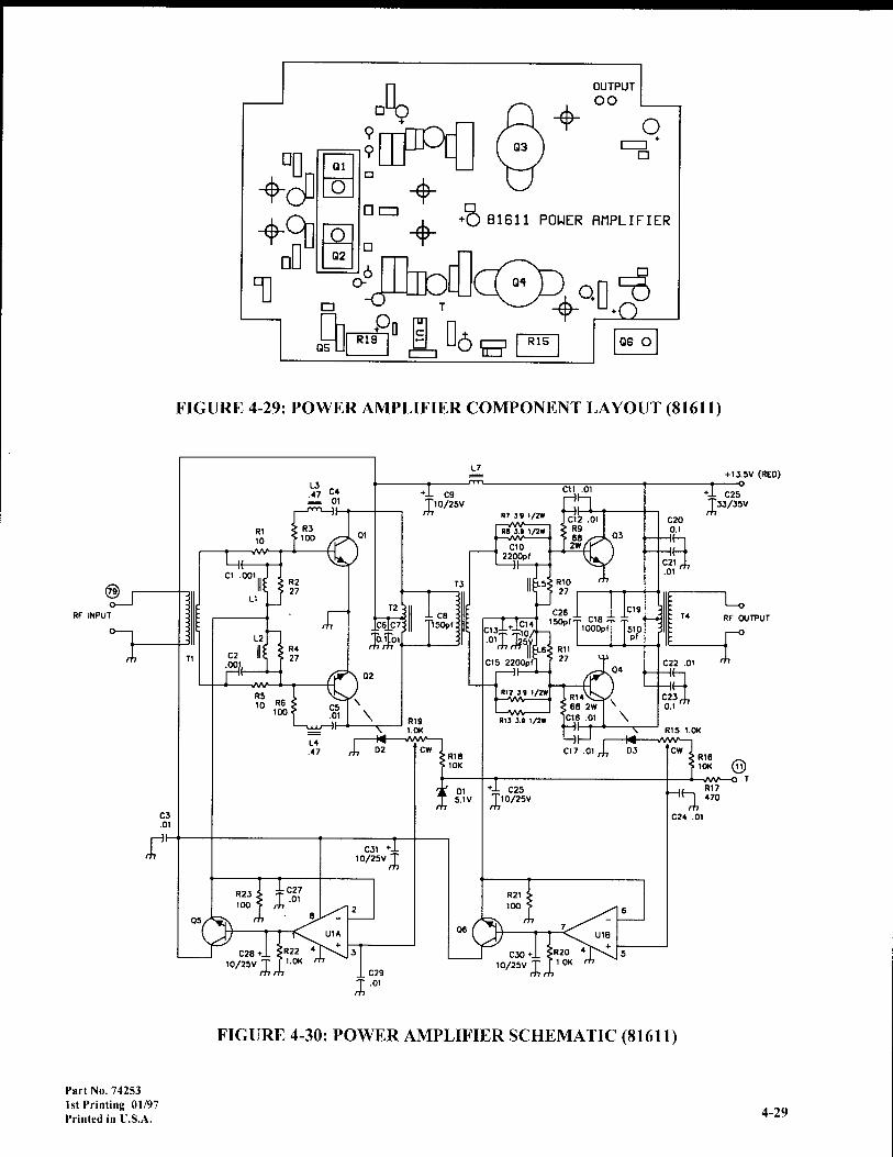
-3t
rffT
i Rro
127I
c26l5Opt
I
iRll>27
R227
R,t27
FIGURE 4-29: POWER AMPLIFIER COMPONENT LAYOUT (81611)
RF OU'PUI
c25o.r
Rr3 r.0K
R't6toK @
OTRl170
cJo1O/25V
Part No. 74253lst Printing 0l/97Printed in U.S.A.
FIGURE 4-30: POWER AMPLIFIER SCHEMATIC (81611)
4-29

4-17 FM BOARD (81598
This module contains circuitry for twoseparate signal paths.
On transmit, connector 75 receives an
amplified microphone signal from the TX Au-dio/BFO board. Amplifier U2A providespreemphasis with a high pass response of typi-cally +6 dB/octave over the 300 to 3000 Hzaudio range. Diodes D4 and D5 limit the peak
to peak amplitude ofthe processed audio to pre-
vent over deviation ofthe FM carrier. Low pass
filter U2B filters harmonic distortion from the
limiter and adjusts the amplitude of the audiofor varactor D6. the varactor performs the volt-age to frequency conversion in the Colpitts os-
cillator Q2.L2 is adjusted to center the oscilla-tor at 9.003 MHz with no audio bias. Buffertransistor Q3 isolates the oscillator and provides
about -5 dBm carrier to the next transmitterstage on the 9 MHz Mixer/IF board via con-nector 33. At this point the transmitter treats
the FM carrier as if it were CW.In receive, the FM receive signal is
tapped off the 9 MHz IF of the noise blankercircuit on the Low Level DriverA{.B. board and
enters the FM board at connector T. The sisnal
feeds Ul, an MC3371P FM receiver chip, which
converts down to a 455 kHz IF frequency. Cer-
amic filter FLI sets the receive bandwidth forthe on-chip quadrature detector. T1, the quadra-
ture coil, is adjusted for maximum recovered
audio and minimum distortion. The audio sig-
nal is deemphasized by the low pass networkof R6, C5 and C6 and is carried on to the IF/AFboard through connector U. The wideband au-
dio signal is also fed through R5-C4, to pin l0of U1, which contains an internal opamp used
as a noise triggered squelch. Output of the in-ternal opamp at pin 1 1 is routed through C2 to
Dl and through connector R to the front panel
mounted SQUELCH control. When the ampli-tude of the audio is below the level set by the
squelch control diode D I conducts and pulls pin12 low, allowing Ul to mute the audio output.
Ul also provides an S-meter output con-
trol current at pin 13. This current is propor-
tional to the logarithm of the IF input signalamplitude, and is fed to buffer transistor Ql.Diode D2 is used to compensate for the base-
emitter voltage drop of Ql, and potentiometerR8 is used to calibrate the S-meter reading. S-
meter output from Ql is sent through connec-
tor V to the front panel meter switch.
Part No. 74253lst Printing 0l/97Printed in U.S.A.4-30

F"{sr Eo -,,8.=o- -,
o-srT+ry n[#,FJ$q,trl=lY- :o n t5-b-=o?oo I la 381ss8 FN BORRD u r." E,*rF= ! - : = "4
L ? .', -l'Bdo @t-uu Uo ,.o lTl o llo -.'-r!o -,
FIGURE 4-31: FM BOARD COMPONENT LAYOUT (81598)
o€SGriAI(ns L src2aD6,t2,OJ,iJ7, Tr.U2
R2,l7x
@
NOIE: ufllESS OTHERnS€ SP€OF|EOl) CaPAOTmS rN I|CA(TARADS (uF)2) IIDUCTmS D{ lrICR(}IE}{Rl6 (uH)J) nE9STORS n O{rS 5I t,/4f
Ul uCJJTIP n A54sllHZu2 LU3sEN Y2 9.OoJIHZ
or-oJ 2i1t21 FLr tTU435€201,02 rN4r4EDJ
'N'5J 6 2V0,r,05 r[{r4t
D5 SI/CJ2ISPA
R4 470
FU RTautxoo
R6 C5J.J< 0.t
OJ62Y
FU RT
IN
TI
;
Irul
J
TRJ7
@t/fiv
FIFTT
+REG.
o lli,Cl,a1lgv
Part No. 74253lst Printing 01/97Printed in U.S.A.
c2lot D6
c26 Rl4.O$ l0O(
RJJ2Xt
Rl46tFIGURE 4-32: FM BOARD SCHEMATIC (81598)
4-31
FY TTCARTIER

4-18 KEYPAD/ENCODER BOARD (81s89)
This module contains ananay of 44key
switches, l8 LED indicators and a rotary shaft
encoder. The circuit board is mounted to the
rear ofthe front panel keypad bezel and is con-
nected to the Logic board through seven con-
nectors which are accessible through the sub
panel at the rear of the fold down front panel
assembly.The keypad switches are aranged elec-
trically in an array of eleven columns and four
rows. The columns are scanned through con-
nectors 92 and93, and the rows are read through
connector 91. The microprocessor detects a key
closure by strobing each column line low insequence, while watching for a low to appear
on any of the row lines. The location of the clo-
sure is defined by the intersection of the col-
umn and row lines that are simultaneously low.
The Logic board drives the indicator
LEDs through connectors 94,95 and 96. The
LEDs are illuminated by a positive drive volt-age and all cathodes are returned to ground
through connectors 95 and 95.
A rotary encoder is mounted to the key-
pad assembly and its output is routed to con-
nector 98, located on the Logic board.
.o -on EXEI I nI I I IH..I n! I I n[.r nn I n n,pf nn tr n o[[ . trT T TI-I !+Q
s3 .OQ+ n il xgQ+ NH
9t
"h'!- il"lnQ+n
Q+tr
.,.o .,.o .,'o _pntnngsr-'r Til
nl1 Bls's
KEYPRO SUBASSEI1BLY
FTGURE 4-33 KEYPAD/ENCODER BOARD COMPONENT LAYOUT (81589)
4-32
Part No, 74253lst Printing 0l/97Printed in U.S.A.

o
o
o
El\@\E @
E\ @\\
@\ @\@\E\ForcEl
\E
@\E\_-9_Ltgl
\--6_I l7 |
\J-l40 l
o
e
e
o
@\
@\ B\\
FffiI\\
E\\
L}\Fq\
lcLEARl\\
@\\
,ENiEd\
\IGNI \
\@\ @\
\@\
\@\
\@\
\E\
\@\
\E\
\-br \blq\ h
6\ \53\ d\
D --Z- ^lsol '\
@\>\@\
@ 6 o d
TUNE
cw
USB
LSB
FSK
FM
LOCK
xrT
RIT
NAR
.25
cn
1.8
2.4
GND
AV
OLY
GN
MS
GND
Part No. 74253lst Printing 01/97Printed in U.S.A.
FTGURE 4-34 KEYPAD/ENCODER BOARD SCHEMATTC (81sS9)
4-33

4-r9 SWTTCH BOARD (81603)
This module contains two LED indica-tors and five latching push button switcheswhich control the functions of ANTENNAmain/aux, AGC on/off, AGC fast/slow,NOTCH auto/manual, and QSK fast/slow. Thisassembly is mounted on the left front subpaneljust inboard of the main POWER switch.
Switch S 1 is connected to the Low Pass
Filter board by connector 7 and selects eitherthe main or auxiliary antenna for use during re-ceive. LED Dl is turned on when Sl is set tothe AUX position.
AGC on/off switch 52 disables the AGCcircuit on the IF/AF board by grounding theAGC amplifier input through connector 49.
AGC fast/slow switch 53 increases the AGC
decay time in the slow position by grounding
the bottom end of an additional integrating ca-
pacitor in the AGC circuit.NOTCH auto/manual switch 54 con-
nects to the Logic board through connector 48.
When in the AUTO position LEDD} is turned
on and the automatic notch function, imple-mented in the DSP processing circuits, is en-
abled along with the front panel manual notchcontrol. When in MANUAL position only thefront panel manual notch is active.
QSK fasVslow switch 55 also connects
to the Logic board through connector 48. The
setting of this switch is monitored by the mi-croprocessor which adjusts the software con-trolled keying accordingly.
.t=@ E@ @E
FIGURE 4-35 SWITCH BOARD COMPONENT LAYOUT (81603)
-l
trL DIO
EE E- Dloz J
S. ze)
r"*ffi,-TTTT 9lllL-r{t I
fL--.' ll*ollF:tu4l
Dlmt-a
urrN.l,lANTl I rux
I!=29E;;< +o
=o
ooooo2<<o
RI2.2X
sl
trlR2
l.oK
o*JF6eltorr rorrJlr@'lr.o*uorro.IlFbTdEltouro .^[email protected]*
FIGURE 4-36 SWTTCH BOARD SCHEMATTC (81603)
Part No. 74253lst Printing 0l/97Printed in U.S.A.
4-34

4-20 UPPER POT. BOARD (81604)
This module contains two dual concen-tric controls, a latching pushbutton switch andan LED indicator. The board mounts on the leftfront sub panel at the control positions of N.B.and SQL, PBT and NOTCH, and the ATTNswitch.
The ATTN switch Sl is wired to theBPF/ Front End board by connector 18 whereit controls the insertion of the receiver attenua-tor pad. When the pad is inserted, Sl applied+13.5 Volts to the anode of -20dB indicatorLED Dl and also to the attenuator switchinscircuit on the BPF/Front End board.
The N.B. control RIA connects to theLow Level DriverA,l.B. board through connec-tor 67 . This control adjusts the input threshold
level of the noise blanker amplifier.The SQL control RIB is connected to
the FM board through connector R, and adjuststhe squelch noise threshold of the FM receiverchip.
NOTCH control R2B, through connec-tor 53 to the IF/AF board, varies a dc voltage toa clock oscillator which determines the fre-quency ofthe manual audio notch filter. Clock-wise rotation of R2B increases the voltage atthe wiper, increasing the notch frequency.
The PBT control R2A connects to thePass Band Tuning board through connector 42,where it controls the dc bias to the 15.3 MHzpass band tuning VCXO. Clockwise rotation ofR2A increasesthe voltage onthe wiper, increas-ing the frequency of the VCXO.
Qa,e e2iir
@ tT?-ilttlTtl
I r:r1lllrlI ;lrllorlL_Vfr
-zoau liiir'i.l
9;9 =ddd-q.aaazzz
=9 --x555i?iooo@@@zzzttt
@
.EOO-6r @E=.UE
R2A10K
R28
10K
'F tr 816aq
FIGURE 4-37: UPPER POT. BOARD COMPONENT LAYOUT (31604)
f soll l-NorcTl
UPPER pOT. BOARD SCHEMATIC (81604)
I soll
Part No. 74253lst Printing 0l/97Printed in U.S.A. 4-35
FIGURE 4-38:

4-21LOWER POT. BOARD (81605)
This module contains two dual concen-
tric controls, a latching pushbutton switch, and
two LED indicators. The board mounts on the
left front panel at the control positions of MICand PWR, AF and RF, ALC indicator, and the
PROC on/off switch and indicator.When PROCessor on/off switch S I is
in the "on" position, "+REG" voltage is appliedto the anode of LED Dl and, through connec-
tor 70, to a diode on the TX Audio board whichroutes processed audio to MIC gain control R1Avia cable 71. RIA sets the level of the signalreturnins on cable 71 to the balanced modula-
tor. When Sl is in the "off " position, indicatorD1 is extinguished, and unprocessed transmit
audio is routed though RIA to the balanced
modulator.PWR control RIB forms a voltage di-
vider, through connector 29 to the 9 MHzMixer/lF board, which sets the ALC threshold.ALC action develops a current through connec-
tor 28 which illuminates ALC indicator D2.
AF gain and RF gain controls, R2A and
R2B, form voltage dividers, through connec-
tors 55 and 50 to the IF/AF board, which deter-
mine respectively audio output level and AGCresting voltage.
E@Erf@@E @-rE@ [,]
B16as @[-|L Dlor K
FIGURE 4-39: LOWER POT. BOARD COMPONENT LAYOUT (81605)
oN lFRocl
3I<F
t??l...{+ffiIItlII|ltltltl
ItlNi<-J
@
i=i.=i\o==:o:LGILLLeeE<< <
ex XcTI :S6 .' " O o oz==zJJo:to<<
o
oo>o8u8Pc +zc
@
4-36
Part No. 74253lst Printing 01/97Printed in U.S.A.
FIGURE 4-40: LOWER POT. BOARD SCHEMATIC (81605)

February 2006 was magic for Scott Robbins, W4PA. Most folkstravel to Barbados to marvel in the Caribbean splendor. But, notScott. Operating as 8P9PA in the ARRL DX CW contest, 5206 QSOsin 48 hours is what it took to win #1 World Single Op. Scott hadreached a goal he set for himself decades earlier as a teenage ham.
Corner Scott at a hamfest, and ask him how he did it. Like any experienced contester, he’ll tell you, “you can’t work ‘em if you can hear ‘em!” He will also tell you his ORION II is the finest contestrig ever built. Believe him, he has personally used them all. To befair, Scott is a bit prejudiced. His day job as TEN-TEC’s Amateur
Radio Product Manager gave him a pivotal role in the developmentof the ORION II. All the hams here at TEN-TEC join in congratulatingScott on two great achievements—his #1 World Single Op and forhis invaluable contribution to the world’s finest HF transceiver.
Call us today at (800) 833-7373 to put an Orion II in yourshack. $3995* or $4295* with automatic antenna tuner.
Ask about our 4-month finance plan.
800-833-7373www.tentec.com
InStock
LimitedQuantity
FACTORYRECONDITIONED
ORION I’S!Immediate Shipment!
1185 Dolly Parton Parkway • Sevierville, TN 37862Sales Dept: 800-833-7373 or [email protected] • M–F 8:00–5:30 EasternService Dept: 865-428-0364 or [email protected] • M–F 8:00–5:00 EasternWe accept VISA, Mastercard, Discover, and American ExpressOffice: (865) 453-7172 • FAX: (865) 428-4483*Shipping is additional. TN residents add 9.5% TN sales tax.
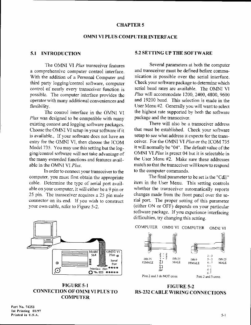
CHAPTER 5
OMNI VI PLUS COMPUTER INTERFACE
5.1 INTRODUCTION
The OMNI YI PIus transceiver featuresa comprehensive computer control interface.With the addition of a Personal Computer andthird party logging/control software, computercontrol of nearly every transceiver function ispossible. The computer interface provides theoperator with many additional conveniences andflexibility.
The control interface in the OMNI VIPlus was designed to be compatible with manyexisting contest and logging software packages.Choose the OMNI VI setup in your software if itis available., If your software does not have anentry for the OMNI VI, then choose the ICOMModel 735. You may use this setting but the log-ging/control software will not take advantage ofthe many extended functions and features avail-able in the OMNI YI Plus.
In order to connect your transceiver to thecomputer, you must first obtain the appropriatecable. Determine the type of serial port avail-able on your computer, it will either be a9 pin or25 pin. The transceiver requires a 25 pin maleconnector on its end. If you wish to constructyour own cable, refer to Figure 5-2.
FIGURE 5-1CONNECTION OF OMNI VI PLUS TO
COMPUTER
Part No. 74253lst Printing 0l/97Printed in U.S,A.
5.2 SETTING UP THE SOFTWARE
Several parameters at both the computerand transceiver must be defined before commu-nication is possible over the serial interface.Check your software package to determine whichserial baud rates are available. The OMNI VIP lus will accommod ate 1200, 2400, 4800, 9600and 19200 baud. This selection is made in theUser Menu #2. Generally you will want to selectthe highest rate supported by both the softwarepackage and the transceiver.
There will also be a transceiver addressthat must be established. Check your softwaresetup to see what address it expects for the trans-ceiver. For the OMNI YI Plus or the ICOM 735it will normally be "04". The default value of theOMNI YI Plus is preset 04 but it is selectable inthe User Menu #2. Make sure these addressesmatch so that the transceiver will know to respondto the computer commands.
The final parameter to be set is the "CdE"item in the User Menu. This setting controlswhether the transceiver automatically reportschanges made from the front panel over the se-rial port. The proper setting of this parameter(either ON or OFF) depends on your particularsoftware package. If you experience interfacingdifficulties, try changing this setting.
COMPUTER OMNI VI COMPUTER
DB-25FEMALE
2-33 - 2 DB-255 -'7 MALErl4l6J
DB-9FEMALE
7-741
61A -.1id
DB-25MALE
Pins 2 and 3 do NOT cross Prns2and3cross
FIGURE 5-2RS-232 CABLE WIRING CONNECTIONS
OMNI
r-- Model llllllllllll OMNI VI
:s64 llllllllllilprus6I rr l$llllilllt Senal@
=_+H jiltililtilt ;;
Int"rl"c" po.t oooof:" Inlerlacc porteccooV Oqe ooooo
5-l
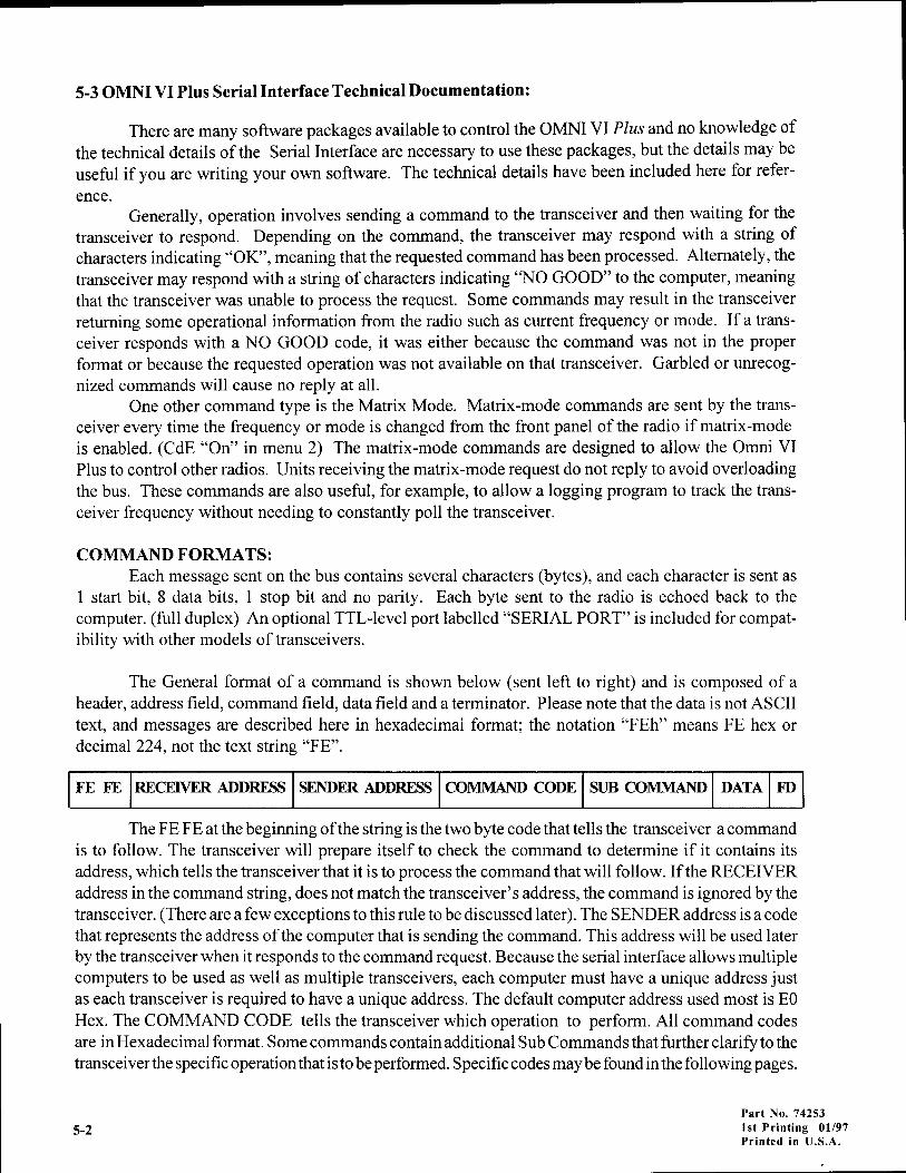
5-3 OMNI VI Plus Serial Interface Technical Documentation:
There are many software packages available to control the OMNI YI Plus and no knowledge ofthe technical details of the Serial Interface are necessary to use these packages, but the details may be
useful if you are writing your own software. The technical details have been included here for refer-
ence.
Generally, operation involves sending a command to the transceiver and then waiting for the
transceiver to respond. Depending on the command, the transceiver may respond with a string ofcharacters indicating "OK", meaning that the requested command has been processed. Alternately, the
transceiver may respond with a string of characters indicating'NO GOOD" to the computer, meaning
that the transceiver was unable to process the request. Some commands may result in the transceiver
returning some operational information from the radio such as current frequency or mode. If a trans-
ceiver responds with a NO GOOD code, it was either because the command was not in the proper
format or because the requested operation was not available on that transceiver. Garbled or unrecog-
nized commands will cause no reply at all.One other command type is the Matrix Mode. Matrix-mode commands are sent by the trans-
ceiver every time the frequency or mode is changed from the front panel of the radio if matrix-modeis enabled. (CdE "On" in menu 2) The matrix-mode commands are designed to allow the Omni VIPlus to control other radios. Units receiving the matrix-mode request do not reply to avoid overloading
the bus. These commands are also useful, for example, to allow a logging program to track the trans-
ceiver frequency without needing to constantly poll the transceiver.
COMMAND FORMATS:Each message sent on the bus contains several characters (bytes), and each character is sent as
1 start bit, 8 data bits, 1 stop bit and no parity. Each byte sent to the radio is echoed back to the
computer. (full duplex) An optional TTl-level port labelled "SEzuAL PORT" is included for compat-ibility with other models of transceivers.
The General format of a command is shown below (sent left to right) and is composed of aheader, address field, command field, data field and a terminator. Please note that the data is not ASCIItext, and messages are described here in hexadecimal format; the notation "FEh" means FE hex ordecimal 224.notthe text string "FE".
The FE FE at the beginning ofthe string is the two byte code that tells the transcerver a commandis to follow. The transceiver will prepare itself to check the command to determine if it contains itsaddress, which tells the transceiver that it is to process the command that will follow. If the RECEIVERaddress in the command string, does not match the transceiver's address, the command is ignored by thetransceiver. (There are a few exceptions to this rule to be discussed later). The SENDER address is a codethat represents the address of the computer that is sending the command. This address will be used laterby the transceiver when it responds to the command request. Because the serial interface allows multiplecomputers to be used as well as multiple transceivers, each computer must have a unique address justas each transceiver is required to have a unique address. The default computer address used most is E0Hex. The COMMAND CODE tells the transceiver which operation to perform. All command codes
are in Hexadecimal format. Some commands contain additional Sub Commands that further clarify to thetransceiverthe specific operationthat isto beperformed. Specific codes maybe foundinthe followingpages.
Part No. 74253lst Printing 01/97Printed in U.S.A.
FE FE RECEIVER ADDRESS SEI.{DER ADDRFSS COMMAND CODE SUB COMMAI\D DATA FD
5-2

TheDATAportionofthecommandstringisrequiredbysomecommands.Itwillcontainfrequencyormode information ifsuchcommandsare issued. TheFD Hex. atthe endofthecommand string, informsthetransceiverthat the end ofthe command has beenreached. Afteratransceiverreceives acomplete commandstring. it will process the command.
5.4 RESPONSE STRINGS - RADIO TO COMPUTERAfter a transceiver has processed a command sent from a computer, it will send a response back
to the computer that originated the command. This insures that the computer knows how the transceiverhandled the command and also provides a method of pacing the commands because the computer knowsnot to send additional commands until it has received a response from the transceiver concerning the lastcommand sent. If a computer sends a command to a transceiver that is not a status requesting command(a command that requests data to be sent back) the transceiver will respond either with a code indicatingOK ( FB Hex.) orNO GOOD (FA Hex.). The returned string will have the following format. The samegeneral structure as described above is maintained but the transceiver is now the sender and the computeris now the receiver.
FEh FEI RECEIVER ADDRESI SENDER ADDRES! FAh or FBI FDh
5.5 DATA FORMATSWhen a computer sends frequency or mode setting commands to a transceiver, the command
string will necessarily contain the requested frequency data or mode code. Frequency data must beencoded as a string of BCD digits in the order shown below. Each Hexadecimal number contains 2 BCDdigits and must be properly encoded for the transceiver to process them. When frequency data isrequested from a transceiver, it will also be in this format.
ndb 4rh
l?Hz 1Hz lKhz l00hz l00Khz l0Khz 10Mhz lMhz lGHz 100MHz
FOR EXAMPLE: The frequency 14.03567 Mhz would be encoded as follows:70 56 03 14 00
Since the TEN-TEC Model 563 has a tuning resolution of 10 Hz, and an upper frequency limitof 30 Mhz, the lHz digit is ignored and attempting to go beyond 30 Mhz will generate a'NO GOOD'response from the transceiver.
When a mode selection command is sent, the mode must be encoded according to the followingtable:
When a transceiver returnsin this format.
its current operating mode to a computer, it will also be encoded
Part No. 74253lst Printing 0l/97Printed in tl.S.A. 5-3

When a filter selection commanc
ine table:
When a transceiver returns its current operating
format.The narrow filters are not supported through the
is sent, the filter must be encoded according to the follow-
2.4kHz 021.8 kHz 03
.5 kHz 04
.25kHz 05
filter to a computer, it will also be in this
serial interface.
5.6 COMMANDSSpecific transceiver control commands can be found on the following pages. In
command must adhere to the structure discussed earlier. Included with the commands
discussion of the possible transceiver response.
use,
isaeach
brief
Part No. 74253lst Printing 0l/97Printed in U.S,A.
Here is a commandkeply example:The command to change modes via the serial interface is 06h, so to change the mode to USB with
a 1.8 kHz filter, the message from the computer to the transceiver is:
FEh FEh 04h EOh 06h 01h 03h FDh
This string is sent as 8 bytes of data with no carriage return or linefeed.
The transceiver will respond with:
FEh FEh EOh O4h FBh FDh
The FBh is the "good" code, and no data follows it. If the command to change modes contained
an incorrect mode number, for example, the transceiver would have responded with:
FEh FEh E()h O4h FAh FDh
Which is the "no good" code.
O3h QUERY TRANSCEIVER FREQUENCY
This command sends the transceiver's current operating frequency to the requesting com-
puter. The frequency data is returned as a string of BCD digits encoded as discussed previously.
COMMAND STRING SENT TO THE TRANSCEIVER:FEh FEh RA SA O3h FDhFEh FEhRASA03hFDh
Command PrefixReceiver Address (transceiver's address)
Sender Address (computer EOh)
Command code for frequency queryCommand String Terminator
5-4

RESPONSE STRING SENT TO THE COMPUTER:The transceiver will respond by sending a return string that contains a data segment with the
transceiver's frequency encoded in BCD format. The returned frequency represent the frequency of thecurrently active VFO.
FEh FEh RA SA DATA FDhFEh FEh Command PrefixRA Receiver Address (computer E0h)SA Sender Address (Transceiver's address)03h Command echoDATA Transceiver's frequency in BCD formatFDh Command strins terminator
O4h QUERY TRANSCEIVER MODE
This command sends the transceiver's current operating mode and filter to the requestingcomputer.
COMMAND STRING SENT TO THE TRANSCEIVER:FEhFEh RA SAO4h FDhFEh FEh. Command PrefixRA Receiver Address (transceiver's address)SA Sender Address (computer EOh)04h Command code for mode queryFDh Command String Terminator
RESPONSE STRING SENT TO THE COMPUTER:The transceiver will respond by sending a return string that contains a data segment with the
transceiver's mode and filter encoded. The data returned is from the displayed VFO.FEh FEh RA SA DATA FDhFEh FEh Command PrefixRA Receiver Address (computer EOh)SA Sender Address (Transceiver's address)04h Command echoDATA Transceiver's mode and filter encodedFDh Command Strine Terminator
This command updates the frequency of the currently selected VFO to data containedin the command string. Frequency data must be encoded.COMMAND STRING SENT TO THE TRANSCEIVER:
FEh FEh RA SA O5h DATA FDhFEh FEh Command PrefixRA Receiver Address (transceiver's address)
Part No. 74253lst Printing 0l/97Prrnted in U.S.A, t-5

SA Sender Address (comPuter E0h)
05h Command code for set frequencY
DATA BCD encoded frequencY data
FDh Command String Terminator
RESPONSE STRING SENT TO THE COMPUTER:The transceiver will send a string that contains either the OK code (FBh) or a NO GOOD code
(FAh) if the operation failed. The operation will fail if the frequency data indicates a frequency that is
beyond the capabilities of the transceiver.FEhFEh RA SA FAhorFBh FDhFEh FEh Command PrefixRA Receiver Address (computer E0H)SA Sender Address (transceiver's address)
FAhorFBh NO GOOD CODE or OK CODEFDh Command Strine Terminator
O6h SET TRANSCEIVER MODE
This command changes the mode of the currently selected VFO to data contained in the
command string. Mode data must be encoded.
COMMAND STRING SENT TO THE TRANSCEIVER:FEh FEh RA SA O6h DATA FDhFEh FEh Command PrefixRA Receiver Address (transceiver's address)
SA Sender Address (computer EOh)
06h Command code for mode and filter selectionDATA Desired mode encoded: one byte for mode only or two bytes for mode and
filter selection.FDh Command String Terminator
RESPONSE STRING SENT TO THE COMPUTER:The transceiver will respond by sending a string containing either the OK code (FBh) if the
operation was performed, or a NO GOOD (FAh) code if the operation failed. The operation will fail ifthe requested mode is not available on the transceiver.
FEhFEh RA SA FAhorFBh FDhFEh FEh Command PrefrxRA Receiver Address (computer E0h)SA Sender Address (Transceiver's address)
FAhorFBh NO GOOD CODE or OK CODE.FDh Command Strins Terminator
O7h VFO SELECTION
This command provides for selection of a particular VFO. Besides the VFO selection code 07h,a sub command must be specified that indicates which VFO operation to perform.COMMAND STRING SENT TO THE TRANSCEIVER:
FEh FEh RA SA O7h SC FDhFEh FEh Command PrehxRA Receiver Address (transceiver's address)
Part No. 74253lst Printing 0l/97Printed in U.S.A.5-6

SA07hSC
FDh
Sender Address (computer E0h)Command code for VFO selectionSub-Command:
00h Select VFO AOlh Select VFO BAOh Copies selected VFO to other VFO. ie VFO A: VFO B.BOh Swaps vFo contents. ie vFo A to vFo B and vFo B to VFo A
Command Strins Terminator
Sender Address (computer E0h)Command code for channel selectMemory channel number in BCD formatCommand String Terminator
RESPONSE STRING SENT TO THE COMPUTER:The transceiver responds by sending a string containing either the OK code (FBh) if the
operation was performed, or a NO GOOD code (FAh) if the operation failed. The operation willif the requested mode is not available on the transceiver.
FEhFEh RA SA FAhorFBh FDhFEh FEh Command PrefixRA Receiver Address (computer E0h)SA Sender Address (Transceiver's address)FAhorFBh NO GOOD CODE or OK CODE.FDh Command Strine Terminator
O8h SELECT MEMORY CHANNEL
This command informs the transceiver which memory channel is to be used for subsequentmemory operations. The memory channel number, in BCD format, must be within the memory channellimits of the transceiver or a NO GOOD will be returned.
COMMAND STRING SENT TO THE TRANSCEIVER:FEh FEh RA SA O8h MC FDhFEh FEh Command prefixRA Receiver Address (transceiver's address)SA08hMCFDh
RESPONSE STRING SENT TO THE COMPUTER:
The transceiver responds by sending a string containing eitherthe OK code (FBh) ifthe operationwas performed, or a NO GOOD code (FAh) if the operation failed. The operation will fail if the memorychannel is not available on the transceiver.
FEh FEh RA SA FAh or FBh FDhFEh FEh Receiver Address (computer E0h)SA Sender Address (Transceiver's address)FAhorFBh NO GOOD CODE or OK CODE.FDh Command String Terminator
Prrt No. 74253lst Printing 0l/97Printed in U.S.A. s7

O9h TRANSFER ACTIVE VFO TO MEMORY CHANNEL
This command transfers contents of the active VFO to the pre-specified memory channel. The
memory channel should have been previously set using command 08h. If not, the last accessed memory
channel will be used for the operation.COMMAND STRING SENT TO THE TRANSCEIVER:
FEhFEh RA SAO9h FDhFEh FEh Command Prehx
RESPONSE STRING SENT TO THE COMPUTER:The transceiver responds by sending a string containing eitherthe OK code (FBh) ifthe operation
was performed, or a NO GOOD code (FAh) if the operation failed.FEhFEh RA SA FAhorFBh FDhFEh FEh Command PrefixRA Receiver Address (computer EOh)
SA Sender Address (Transceiver's address)
FAhorFBh NO GOOD CODE or OK CODE.F'Dh Command String Terminator
OAh COPY MEMORY CHANNEL TO ACTIVE VFO
Transceiver to copy data from the pre-specified memory channel into the currently active VFO.The memory channel should have been previously set using command 08h. If not, the last accessed
memory channel will be used for the operation.
COMMAND STRING SENT TO THE TRANSCEIVER:FEh FEh RA SA OAh FDh
RASA09hFDh
FEh FEhRASA0AhFDh
Receiver Address (transceiver's address)
Sender Address (computer E0h)Command code for VFO save
Command Strins Terminator
Command PrefixReceiver Address (transceiver's address)
Sender Address (computer EOh)
Command code for memory recallCommand Strins Terminator
RESPONSE STRING SENT TO THE COMPUTER:Transceiver responds by sending a string containing either the OK code (FBh) if the operation
was performed, or a NO GOOD code (FAh) if the operation failed.FEh FEh RA SA FAh or FBh FDhFEh FEh Command PrefixRA Receiver Address (computer EOh)
SA Sender Address (Transceiver's address)FAhorFBh NO GOOD CODE or Ok CODE.FDh Command Strins Terminator
Part No. 74253lst Printing 0l/97Printed in U.S.A.
5-8

OFh SET/CANCEL SPLIT OPERATION
This command activates or cancels split operation of the transceiver. In addition to the SET/CLEAR SPLIT command code 0Fh, a sub command must be specified to indicate which operation toperform.COMMAND STRING SENT TO THE TRANSCEIVER:
FEh FEh RA SA OFh SC FDhFEh FEh Command PrefixRA Receiver Address (transceiver's address)SA Sender Address (computer E0h)OFh Command code for split operationSC Sub-command:
FDh
Cancel split operationSet split operation
Command Strins Terminator
R-ESPONSE STRING SENT TO THE COMPUTER:Transceiver responds by sending a string containing either the OK code (FBh) if the operation
was performed, or a NO GOOD code (FAh) if the operation failed.FDhFDh RA SA FAhorFBh FDh
00h01h
FD FDRASA
Command PrefixReceiver Address (computer EOh)Sender Address (Transceiver's address)
FAhorFBh NO GOOD CODE or OK CODE.FD Command String Terminator
SPECIALIZED COMMAND MODES:Sometransceivers,suchas TEN-TECmodels 563,564,535and536provideanadditionalmode
referred to as MATRIX MODE. MATzuX MODE allows a transceiver to operate as a controller for othertransceiversconnectedtotheserialinterface. Whenthe transceiverisplacedinMATRIXMODEitwillgenerateand accept MATzuX MODE COMMANDS. These commands are sent from any transceiver placed inMATzuXMODEandareinaformatuniquetoMATzuXMODE. OtherMATRIXMODEtransceiverswillacceptthematrixmodecommandsbutwillnotgenerate response. MATzuXMODEcommandsaregeneratedfrom a MATRIX MODE transceiver when ever its operating status is changed (ie frequency or mode ). BysendingMATzuXMODEcommandsthatcontainthisinformation,otherMATzuXMODEtransceiverswillautomaticallytrackthetransceiverthatgeneratedthecommands."M.Lock"willappearindisplay. ToactivateMATRIX mode on Model 563: in USER'S MENU, turn CdE.,ON',.
OOh MATRIX MODE COMMANDTRANSFER CURRENT OPERATING FREQUENCY TO ALL TRANSCEIVERS INMATRIX MODE
This command, generated by a transceiver in MATRIX MODE. causes any other MATRIXMODE transceiver to mimic the operation of the transceiver that generated this command.COMMAND STRING SENT TO THE TRANSCEIVER:
FEh FEh OOh SA OOh DATA FDh
Part No. 74253lst Printing 0l/97Printed in tt.S.A.
FEh FEh Command Prefix
5-9
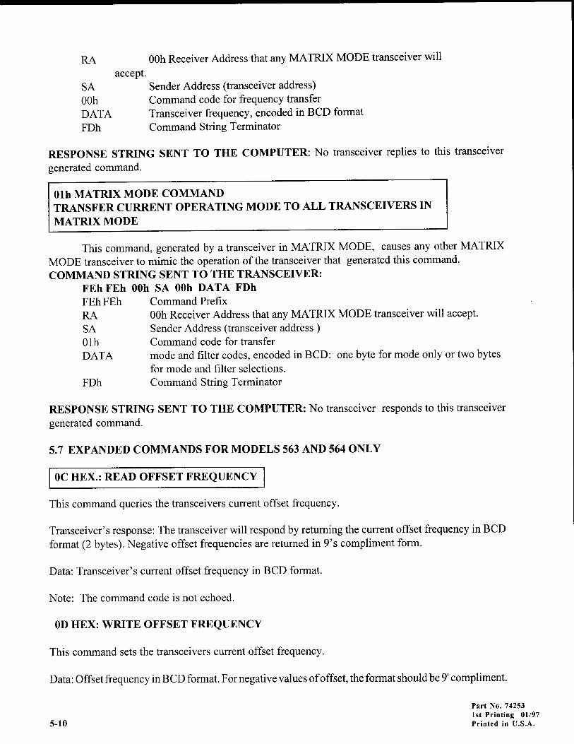
RA
SA00hDATAFDh
00h Receiver Address that any MATRIX MODE transceiver willaccept.
Sender Address (transceiver address)
Command code for frequency transfer
Transceiver frequency, encoded in BCD format
Command Strine Terminator
RESPONSE STRING SENT TO THE COMPUTER: No transceiver replies to this transceiver
senerated command.
Olh MATRIX MODE COMMANDTRANSFER CURRENT OPERATING MODE TO ALL TRANSCEIVERS INMATRIX MODE
This command, generated by a transceiver in MATRIX MODE, causes any other MATRIX
MODE transceiver to mimic the operation of the transceiver that generated this command.
COMMAND STRING SENT TO THE TRANSCEIVER:FEh FEh OOh SA OOh DATA FDhFEhFEh Command PrefixRA 00h Receiver Address that any MATRIX MODE transceiver will accept.
SA Sender Address (transceiver address )01hDATA
FDh
Command code for transfermode and filter codes, encoded in BCD: one byte for mode only or two bytes
for mode and filter selections.Command String Terminator
RESPONSE STRING SENT TO THE COMPUTER: No transceiver responds to this transceiver
generated command.
5.7 EXPANDED COMMANDS FOR MODELS 563 AND 564 ONLY
OC HEX.: READ OFFSET FREQUENCY
This command queries the transceivers current offset frequency.
Transceiver's response: The transceiver will respond by returning the current offset frequency in BCD
format (2 bytes). Negative offset frequencies are returned in 9's compliment form.
Data: Transceiver's current offset frequency in BCD format.
Note: The command code is not echoed.
OD HEX: WRITE OFFSET FREQUENCY
This command sets the transceivers current offset frequency.
Data: Offset frequency in BCD format. For negative values ofoffset, the format should be 9' compliment.
Part No. 74253lst Printing 0l/97Printed in U.S.A,s-10

BOARD REQUIRED)
This command will activate the optional voice board and announce the frequency ofthe cunentVFO.
Transceiver's response: Returns NO GOOD if the voice board is not installed.
16 HEX: SET/CLEAR TRANSMIT MODE
This command and associated sub-commands control the transmitter.
These commands provide remote control of the transmit/receive functions but cannot override localcontrol functions. Thus, if the PTT line is depressed, sending a RETURN TO RECEIVE commandcannot override the PTT action.
SUB-COMMAND OlhSUB-COMMAND O2h
GO TO TRANSMITRETURN TO RECEIVE
Transceiver's response: If the transceiver was able to perform the indicated operation, it willreturn the OK code.
COMMAND 17h: RETURN TRANSCEIVER STATUS
This command queries the transceiver's extended status information.
Transceiver's response: The transceiver will return the extended status information encoded ina I byte code encoded as listed below.
FE FE RA SA DATA FD
BIT POSITIONO SPLITSTATUSI2aJ
45
6
VFO SELECTEDTX STATUSRIT STATUSXIT STATUSVOX STATUSLOCK STATUSNOT USED
(0:SPLIT OFF, l:SPLIT ON)(0=VFO A, 1=VFO B)(0:RX, l:TX)(0:OFF, l:ON)(0:OFF, 1:ON)(O=OFF, l=ON)(0:OFF, l:ON)
Note: The command code is not echoed.
I8h: RETURN TRANSMIT FREQUENCY
This command returns the true transmit frequency ofthe transceiver. Any transmit offset or split statuswill be included in the returned frequency.
Part No. 74253lst Printing 0l/97Printed in I-l.S,A. 5-t I

COMMAND STRING SENT TO THE TRANSCEIVER:FEh FEh RA SA T8h FDhFEh FEhRASAl8hFDh
Command PrefixReceiver Address (transceiver's address)
Sender Address (computer EOh)
Command code for frequency queryCommand String Term inator
Receiver Address (computer EOh)
Sender Address (Transceiver's address)Transceiver's frequency in BCD formatCommand strins term inator
Command PrefixReceiver Address (transceiver's address)Sender Address (computer EOh)
Command code for frequency queryCommand String Term inator
RESPONSE STRING SENT TO THE COMPUTER:The transceiver willrespond by sending a return string that contains a data segmentwith the transceiver's
frequency encoded in BCD format. The returned frequency represents the frequency ofthe currently active VFO.FEh FEh RA SA DATA FDhFEh FEh Command PrefixRASADATAFDh
RESPONSE STRING SENT TO THE COMPUTER:The transceiver will respond by sending a return string that contains a data segment with the
transceiver's frequency encoded in BCD format. The returned frequency represent the frequency of thecurrently active VFO.
FEh FEh RA SA DATA FDhFEh FEh Command PrefixRA Receiver Address (Computer EOh)
SA Sender Address (Transceiver's address)DATA Transceiver's frequency in BCD formatFDh Command stringterminator
Part No. 74253lst Printing 0l/97Printed in U.S.A.
Note: Command 03h is echoed as if this were a 03h query.
19h: RETURN RECEM FREQUENCY
This command returns the true receive frequency of the transceiver. Receive offset and split operationare included in the returned frequency.
COMMAND STRING SENT TO THE TRANSCEIVER:FEh FEh RA SA I9h FDhFEh FEhRASA03hFDh
5-12
Note: Command code 03h is echoed as if this were a 03h query.

CHAPTER 6
TROUBLE SHOOTING PROCEDURES
If the transceiver should fail to operate normally, use the following chart as
determining the problem. Often the cause of the problem is an overlookedcontrol or a mistake in entering information into the keypad. Of course, youthe Service Department (l -423-428-0364) and ask for assistance should you
an aid inswitch /may callneed it.
SYMPTOM POSSIBLE CAUSE
Transceiver dead. no meter lamp, no - Quickly Reset microprocessor withdisplay Master Reset (2-4.2)
- Check power switches on radio andpower supply
- Check power cable to radio- Check fuses on radio and power
supply- Check polarity and correct voltage of
power supply- Check wall outlet for power supply- Be sure Ten-Tec power supply is not
tripping off due to high SWR (l -2)
Transceiver OK, no meter lamp or - IN+ function (in USER MENU 1) set todisplay (or very low) minimum (3- l . l6)
Receiver dead,display on
meter lamp and Check AF and RF GAIN controls C-s.09)Check headphone and EXTERNALSPKR jacks. (3-6.01)Check to be sure radio is not inTRANSMITCheck CRYSTAL FILTER SELEC-TION. Be sure filter is installed.(1-8) (3-1.08)Check MAIN / AUX Antenna switchfor proper antenna selection (3-5.15)Check Antenna coax and associateditems.Check PBT control (should be cen-tered) (3-5.12)If in FM, check SQUELCH (3-5.1 I )Check MUTE jack, if used (3-6.10)
Part No. 74253lst Printing 0l/97Printed in U.S,A.

TROUBLE SHOOTING PROCEDURES (Cont.)
SYMPTOM POSSIBLE CAUSE
Weak Receive Check MAIN / AUX Antenna switchfor proper antenna selection (3-5.15)Check RF GAIN control (3-5.09)Check ATTN switch (3-5.05)Check for proper CRYSTAL FILTERselection (3-I.08)Check PBT control (should be cen-
tered) (3-5.12)Check Antenna coax and accociateditems
Distorted Received CW / AMTOR /PACKET / RTTY sisnals
Check AUTO NOTCH switch(should be off) (3-5.13)Check AGC ON / OFF switch(should be on) (3-5.07)
Distorted Received SSBSignals
Check AGC ON / OFF switch(should be on) (3-5.07)May need to activate -20 dBATTENUATOR (3-s.0s)Check for proper mode selection(3-1.02)
Transmit frequency differentfrom Receive frequency
Check SPLIT function (3-2.2)(normally OFF)Check RIT / XIT (3-2.3,3-2.4)
Distorted Transmit signals Check ground systemCheck antenna system SWRCheck for strong RF field in shackReset microprocessorPROCESSOR level turned up toohigh (3-s.04)
Frequencies will not storein memories
- Be sure to press M>VFO keyquickly. If button held too long,frequency will go to SCRATCH PADMEMORY (3-3.3)
Main or remotewill not change
tuning knobfrequency
Check LOCK (normally OFF)Be sure you are not in VOX SETUProutine (3- I .09)
- Be sure you are not in SIDETONESETUP routine (3-1.11)
Part No. 74253lst Printing 01/97Printed in tl.S.A.
6-2

TROUBLE SHOOTING PROCEDURES (Cont.)
SYMPTOM POSSIBLE CAUSE
Keypad will not respond to input,main tuning knob will not changefrequency
No readout, audio present
Readout present, can not entercommands
- Reset microprocessor with PARTIALRESET. If radio still does notrespond, use a MASTER RESET.(2-4)
- USER OPTIONS MENU activated(3-4)
Clock resets to l2:00 when radioturned off
Memories and USER Optionsclear out when radio turned off
Replace 3 volt Lithium battery(CR-2032;DL-2032) on Logic Board(81606). See pg 4-18 &.4-19.
Beep heard every l0 - minutes ID timer turned on in USEROPTIONS MENU G-4\
Linear amplifier will not key usingRELAY N. O. jack on rear panel
- LCO option in USER OPTIONSMENU not turned ON (3-4)
Linear amplifier will not key usingTX OUT / TX EN jacks ( TEN-TECLINEARS)
Be sure TX OUT / TX EN cablesare not swapped. (3-6.09)Check TX OUT / TX EN cablecontinuity
Radio stays in Transmit whenturned on
Check CW KEY / KEYER PADDLEcable for shortCheck PTT line (cable) for shortCheck mic cable for short on pTTwire (pin 3)Check computer terminal unitfor short on PTT line.Check VOX GAIN, if used (3-1.09)
Part No. 74253lst Printing 0I/97Printed in U.S.A. 6-3

TEN-TEC, Inc.I 185 Dolly Parton ParkwaySevierville, TN 37862
CUSTOMER SERVI TELEPHONE423-42
LIMITED WARRANTY AND SERVICE POLICY. U.S.A.
TEN-TEC,Inc. warrants this product to be free from defects in material andofone year from the date ofpurchase, under these conditions:
for a period
l. THIS WARRANTY APPLIES ONLY TO THE ORIGINAL OWNER. It is that the war-ranty registration card be sent to us promptly to establish you as the owner ofinsure that any bulletins pertaining to this equipment will be sent to you.
This will also
2. READ THE MANUAL THOROUGHLY. This warranty does not cover damage rgsulting from im-proper operation. Developing a thorough understanding of this equipment is your responsibility.
3. IF TROUBLE DEVELOPS we recommend that you contact our customer service lroup direct. Theselling dealer is not obligated by us to perform service in or out of warranty. It has beon our experiencethat factory direct service is expeditious and usually results in less down-time on the gquipment. Somedealers do offer warranty service and of course, have our complete support.
4. WE ENCOURAGE SELF HELP. Taking the covers off does not void the warranty. In many cases
our customer service technicians, with your help, can identify a faulty circuit board. In these cases wewill send you a replacement board which you can change out. This will be shipped on a 30 day memobilling and when the defective board is returned, we will issue credit.
5. EQUIPMENT RETURNED TO THE FACTORY must be properly packaged, preferably in the origi-nal shipping carton. You pay the freight to us and we prepay surface freight back to you.
6. EXCLUSIONS. This warranty does not cover damage resulting from misuse, lightning, excess volt-ages, polarity errors or damage resulting from modifications not recommended or approved by Ten-Tec.In the event of transportation damage a claim must be filed with the carrier. Under no circumstances isTen-Tec liable for consequential damages to persons or property caused by the use of this equipment.
7. TEN-TEC RESERVES the right to make design changes without any obligation to modify equipmentpreviously manufactured.
8. THIS WARRANTY is given in lieu of any other warranty, expressed or implied.
SERVICE OUTSIDE OF THE U.S.A.
Many of our dealers provide warranty service on the equipment they sell. Many of them also provideout of warranty service on all equipment whether they sold it or not. If your dealer does not provideservice or is not conveniently located, follow the procedure outlined above. Equipment returned to uswill be given the same attention as domestic customers but all freight expense, customs and brokerfees will be paid by you.
Part No. 74244

This obsolete manual file is provided as a courtesy to you by Ten-Tec, Inc.
Ten-Tec's service department can repair and service virtually everything we have built going back to our first transceivers in the late 1960's. It is our ability to continue offering service on
these rigs that has led to their re-sale value remaining high and has made a major contribution to our legendary service reputation.
Printed and bound copies of all manuals are available for purchase through our service department if you would prefer not to use this copy as your transceiver manual.
We can repair or service your Ten-Tec equipment at our facility in Sevierville, TN. We also offer support via telephone for all products via during usual business hours of 8 a.m. to 5 p.m. USA
Eastern time, Monday through Friday. We have a large supply of parts for obsolete products. Repairing a transceiver or amplifier yourself? Contact us for parts pricing information.
Service department direct line: (865) 428-0364Ten-Tec office line: (865) 453-7172
Service department email: [email protected] Address: 1185 Dolly Parton Parkway, Sevierville, TN 37862 USA
We have found it is most effective for us to help you troubleshoot or repair equipment with a consultation via telephone rather than by email.
Suggested contact methods are:
Troubleshooting or repairing equipment – call (865) 428-0364Other inquiries – call (865) 428-0364 or email [email protected]
THANK YOU AND 73 FROM ALL OF US AT TEN-TEC