this is an author-created, un-copyedited version of an
TRANSCRIPT

This is an author-created, un-copyedited version of an article accepted for publication in 2D Materials. The publisher is not responsible for any errors or omissions in this version of the manuscript or any version derived from it. The Version of Record is available online at https://doi.org/10.1088/2053-1583/1/3/035003. Polarization doping of graphene on silicon carbide Samir Mammadov, Jürgen Ristein, Roland J Koch, Markus Ostler, Christian Raidel, Martina Wanke, Remigijus Vasiliauskas, Rositza Yakimova and Thomas Seyller 2D Materials 1 (2014) 035003
Polarization Doping of Graphene on Silicon Carbide
Samir Mammadov1, Jurgen Ristein2, Roland J. Koch1,Markus Ostler1, Christian Raidel1, Martina Wanke1,Remigijus Vasiliauskas3, Rositza Yakimova3, and ThomasSeyller1
1 Institut fur Physik, Technische Universitat Chemnitz, Reichenhainer Str. 70,09126 Chemnitz, Germany2 Lehrstuhl fur Laserphysik, Universitat Erlangen-Nurnberg,Erwin-Rommel-Str. 1, 91058 Erlangen, Germany3 Department of Physics, Chemistry and Biology, Linkoping University,SE-58183, Linkoping, Sweden
E-mail: [email protected],
Abstract. The doping of quasi-freestanding graphene (QFG) on H-terminated,Si-face 6H-, 4H-, and 3C-SiC is studied by angle-resolved photoelectronspectroscopy (ARPES) close to the Dirac point. Using semi-insulating as well asn-type doped substrates we shed light on the contributions to the charge carrierdensity in QFG caused by i) the spontaneous polarization of the substrate, and ii)the band alignment between the substrate and the graphene layer. In this way weprovide quantitative support for the previously suggested model of polarizationdoping of graphene on SiC [Phys. Rev. Lett. 108, 246104 (2012)].
Keywords: graphene, silicon carbide, doping, ARPES, XPS
Submitted to: 2D Mater.
1. Introduction
Silicon carbide (SiC) crystals have evolved as the substrates of choice for graphenegrowth [1–3]. Epitaxial graphene (EG) on SiC has been a subject of intensiveresearch due to various promising applications, such as, e.g., high frequency transistors[4–6], frequency mixers [7] or resistance standards [8]. The process of preciselycontrolling the number of graphene layers [2] and the determination of the basicparameters of the band structure and its dependence on the number of layers [10]or on interface modification is of great importance for the future of carbon-basednanoelectronics. Although different polytypes such as 3C-, 4H- and 6H-SiC areavailable, such fundamental questions as how the charge carrier concentration and typein the graphene layers varies with the substrate polytype and substrate doping remainlargely unanswered. This issue plays a very important role in the research of grapheneon SiC, as well as in its industrial applications. In this study we experimentally
Polarization Doping of Graphene on Silicon Carbide 2
address this issue and create a rational basis for the choice of substrate for futuregraphene-on-SiC applications.
It is well known that EG on SiC(0001), which is situated on top of the so-called buffer layer (denoted by 6
√3 in the figures of this work) is intrinsically n-type
doped [1, 9, 10]. Note that the buffer layer is already a honeycomb lattice of carbonatoms, but on account of hybridization with SiC states it does not exhibit the Dirac-like dispersion at the K-point of the Brillouin zone, [9, 11–13]. A model by Kopylovet al. [14] explained the n-type doping by either bulk or interface donor states.
The situation changes when going from EG on the buffer layer to quasi-freestanding graphene (QFG) on H-terminated SiC(0001) [15–17, 19, 19]. The latteris obtained - as was first shown by Riedl et al. [15, 16] - by annealing the bufferlayer in an atmosphere of hydrogen. Hydrogen intercalates between the SiC surfaceand the buffer layer, saturating the dangling bonds of the topmost Si atoms [21, 22].In that way, the buffer layer is decoupled from the SiC surface. On account of thedramatically reduced interaction of the now H-terminated SiC(0001) surface with thecarbon atoms, an almost undisturbed graphene layer emerges which is referred to asquasi-freestanding graphene. For details about the preparation see also section II. Incontrast to EG, QFG has an excess of holes. This p-type doping cannot be explainedby the model of Kopylov [14]. Instead, it has been attributed to the influence of thespontaneous polarization of the hexagonal SiC substrate [23].
The spontaneous polarization (which is a bulk property) leads to a polarizationcharge on the polar surfaces of hexagonal semiconductor compounds, such asSiC and GaN, which is usually compensated by internal charge formation due todepletion/accumulation of charge carriers or by external buildup of ionic charge on thesurfaces. Only the modulation of the polarization charge at a surface upon an externalperturbation can be measured [24–26], making the effect itself difficult to addressexperimentally. The existence of various SiC polytypes offers an excellent opportunityto address the question. While spontaneous polarization is absent for the cubicpolytype 3C-SiC due to symmetry, it is mainly induced at the inversion of the stackingsequence of the SiC double layers in the hexagonal polytypes. Consequently, varyingthe hexagonality of the SiC polytype changes the polarization proportionally. Thus,for 4H-SiC(0001) it is expected to be 6/4 times larger than for 6H-SiC(0001) [27–30].
In order to test this hypothesis, we have carried out systematic angle-resolvedphotoelectron spectroscopy (ARPES) measurements close to the Dirac point. Inparticular, the comparison of the total charge densities of quasi-freestanding graphene(QFG) on 6H-SiC(0001), 4H-SiC(0001) and 3C-SiC(111) provides a quantitativeconfirmation of the polarization doping proposed earlier [23]. In addition, bycomparing n-type and semi-insulating substrates with identical graphene layers ontop we provide further additional insights into the question how the charge carrierdensity in graphene overlayers is influenced by the doping level of the SiC bulk.
2. Sample Preparation and Characterization
EG was formed by sublimation growth in argon atmosphere [2] on the Si-face of variousSiC substrates. Nitrogen doped n-type 6H-SiC(0001) was purchased from SiCrystalAG while semi-insulating 6H-SiC wafers were obtained from II-VI Inc. Semi-insulatingas well as N-doped, n-type 4H-SiC wafers were purchased from and Cree Inc. Finally,a sample of 3C-SiC with (111) surface orientation grown on a 6H-SiC(0001) substratewas prepared at Linkoping University. Growth of EG (including samples covered by
Polarization Doping of Graphene on Silicon Carbide 3
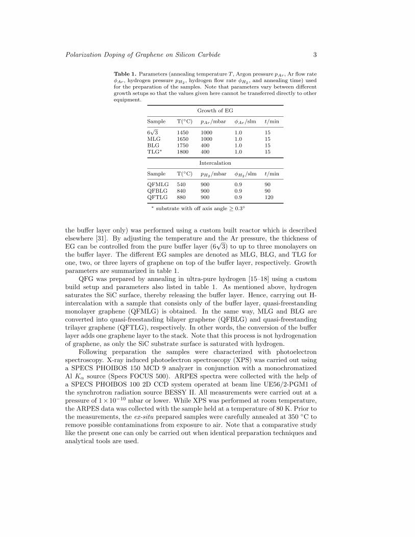
Table 1. Parameters (annealing temperature T , Argon pressure pAr, Ar flow rateφAr, hydrogen pressure pH2
, hydrogen flow rate φH2, and annealing time) used
for the preparation of the samples. Note that parameters vary between differentgrowth setups so that the values given here cannot be transferred directly to otherequipment.
Growth of EG
Sample T(◦C) pAr/mbar φAr/slm t/min
6√
3 1450 1000 1.0 15MLG 1650 1000 1.0 15BLG 1750 400 1.0 15TLG∗ 1800 400 1.0 15
Intercalation
Sample T(◦C) pH2/mbar φH2
/slm t/min
QFMLG 540 900 0.9 90QFBLG 840 900 0.9 90QFTLG 880 900 0.9 120
∗ substrate with off axis angle ≥ 0.3◦
the buffer layer only) was performed using a custom built reactor which is describedelsewhere [31]. By adjusting the temperature and the Ar pressure, the thickness ofEG can be controlled from the pure buffer layer (6
√3) to up to three monolayers on
the buffer layer. The different EG samples are denoted as MLG, BLG, and TLG forone, two, or three layers of graphene on top of the buffer layer, respectively. Growthparameters are summarized in table 1.
QFG was prepared by annealing in ultra-pure hydrogen [15–18] using a custombuild setup and parameters also listed in table 1. As mentioned above, hydrogensaturates the SiC surface, thereby releasing the buffer layer. Hence, carrying out H-intercalation with a sample that consists only of the buffer layer, quasi-freestandingmonolayer graphene (QFMLG) is obtained. In the same way, MLG and BLG areconverted into quasi-freestanding bilayer graphene (QFBLG) and quasi-freestandingtrilayer graphene (QFTLG), respectively. In other words, the conversion of the bufferlayer adds one graphene layer to the stack. Note that this process is not hydrogenationof graphene, as only the SiC substrate surface is saturated with hydrogen.
Following preparation the samples were characterized with photoelectronspectroscopy. X-ray induced photoelectron spectroscopy (XPS) was carried out usinga SPECS PHOIBOS 150 MCD 9 analyzer in conjunction with a monochromatizedAl Kα source (Specs FOCUS 500). ARPES spectra were collected with the help ofa SPECS PHOIBOS 100 2D CCD system operated at beam line UE56/2-PGM1 ofthe synchrotron radiation source BESSY II. All measurements were carried out at apressure of 1×10⁻¹⁰ mbar or lower. While XPS was performed at room temperature,the ARPES data was collected with the sample held at a temperature of 80 K. Prior tothe measurements, the ex-situ prepared samples were carefully annealed at 350 ◦C toremove possible contaminations from exposure to air. Note that a comparative studylike the present one can only be carried out when identical preparation techniques andanalytical tools are used.
Polarization Doping of Graphene on Silicon Carbide 4
3. Results and Discussion
3.1. XPS Analysis
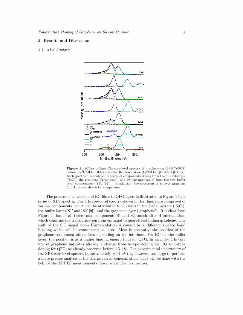
Figure 1. (Color online) C1s core-level spectra of graphene on 6H-SiC(0001)before (6
√3, MLG, BLG) and after H-intercalation (QFMLG, QFBLG, QFTLG).
Each spectrum is analyzed in terms of components arising from the SiC substrate(’SiC’), the graphene (’graphene’), and (where applicable) from the two bufferlayer components (’S1’, ’S2’). In addition, the spectrum of trilayer graphene(TLG) is also shown for comparison.
The process of conversion of EG films to QFG layers is illustrated in Figure 1 by aseries of XPS spectra. The C1s core-level spectra shown in that figure are comprised ofvarious components, which can be attributed to C atoms in the SiC substrate (’SiC’),the buffer layer (’S1’ and ’S2’ [9]), and the graphene layer (’graphene’). It is clear fromFigure 1 that in all three cases components S1 and S2 vanish after H-intercalation,which confirms the transformation from epitaxial to quasi-freestanding graphene. Theshift of the SiC signal upon H-intercalation is caused by a different surface bandbending which will be commented on later. Most importantly, the position of thegraphene component also differs depending on the interface. For EG on the bufferlayer, the position is at a higher binding energy than for QFG. In fact, the C1s coreline of graphene indicates already a change from n-type doping for EG to p-typedoping for QFG, as already observed before [15–18]. The experimental uncertainty ofthe XPS core level spectra (approximately ±0.1 eV) is, however, too large to performa more precise analysis of the charge carrier concentration. This will be done with thehelp of the ARPES measurements described in the next section.
Polarization Doping of Graphene on Silicon Carbide 5
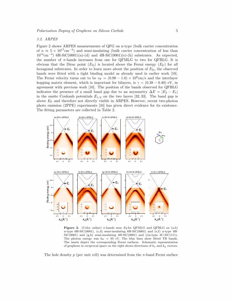
3.2. ARPES
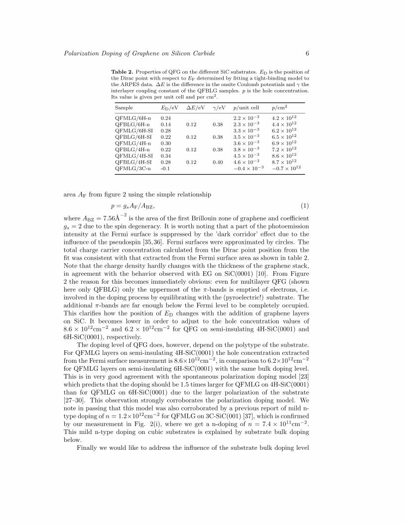
Figure 2 shows ARPES measurements of QFG on n-type (bulk carrier concentrationof n ≈ 5 × 1017cm−3) and semi-insulating (bulk carrier concentration of less than1014cm−3) 6H-SiC(0001)(a)-(d) and 4H-SiC(0001)(e)-(h) substrates. As expected,the number of π-bands increases from one for QFMLG to two for QFBLG. It isobvious that the Dirac point (ED) is located above the Fermi energy (EF) for allhexagonal substrates. In order to learn more about the position of ED, the observedbands were fitted with a tight binding model as already used in earlier work [10].The Fermi velocity turns out to be vF = (0.98 − 1.0) × 108cm/s and the interlayerhopping matrix element, which is important for bilayers, is γ = (0.38 − 0.40) eV, inagreement with previous work [10]. The position of the bands observed for QFBLGindicates the presence of a small band gap due to an asymmetry ∆E = |E2 − E1|in the onsite Coulomb potentials E1/2 on the two layers [32, 33]. The band gap isabove EF and therefore not directly visible in ARPES. However, recent two-photonphoto emission (2PPE) experiments [34] has given direct evidence for its existence.The fitting parameters are collected in Table 2.
ED ED
EDEDED ED
Bin
din
g e
nerg
y (e
V)
ED
-0.1 0 0.1-0.1 0 0.1-0.1 0 0.1-0.1 0 0.1
-0.1 0 0.1-0.1 0 0.1-0.1 0 0.1
kx(Å-1)kx(Å
-1)kx(Å-1)kx(Å
-1)
-1.5
-1.0
-0.5
0
0.5
(a) 6H-n QFMLG (b) 6H-n QFBLG (c) 6H-SI QFMLG (d) 6H-SI QFBLG
(e) 4H-n QFMLG (f) 4H-n QFBLG (g) 4H-SI QFMLG (h) 4H-SI QFBLG
-0.1 0 0.1
kx(Å-1)
(i) 3C-n QFMLG
-0.1 0 0.1
ED
-0.1 0 0.1
1.6
1.7
1.8
K
MΓ
ky
kx
-0.1 0 0.1
1.6
1.7
1.8
1.6
1.7
1.8
-0.1 0 0.1-0.1 0 0.1
1.6
1.7
1.8
-0.1 0 0.1 -0.1 0 0.1
1.6
1.7
1.8
1.6
1.7
1.8
-0.1 0 0.1
1.6
1.7
1.8
-0.1 0 0.1
Figure 2. (Color online) π-bands near EFfor QFMLG and QFBLG on (a,b)n-type 6H-SiC(0001), (c,d) semi-insulating 6H-SiC(0001) and (e,f) n-type 4H-SiC(0001) and (g,h) semi-insulating 4H-SiC(0001) and (i)n-type 3C-SiC(111).The photon energy was ~ω = 95 eV. The blue lines show fitted TB bands.The insets depict the corresponding Fermi surfaces. Schematic representationof graphene in reciprocal space on the right shows directions of kx and ky vectors.
The hole density p (per unit cell) was determined from the π-band Fermi surface
Polarization Doping of Graphene on Silicon Carbide 6
Table 2. Properties of QFG on the different SiC substrates. ED is the position ofthe Dirac point with respect to EF determined by fitting a tight-binding model tothe ARPES data. ∆E is the difference in the onsite Coulomb potentials and γ theinterlayer coupling constant of the QFBLG samples. p is the hole concentration.Its value is given per unit cell and per cm2.
Sample ED/eV ∆E/eV γ/eV p/unit cell p/cm2
QFMLG/6H-n 0.24 2.2× 10⁻³ 4.2× 10¹²
QFBLG/6H-n 0.14 0.12 0.38 2.3× 10⁻³ 4.4× 10¹²
QFMLG/6H-SI 0.28 3.3× 10⁻³ 6.2× 10¹²
QFBLG/6H-SI 0.22 0.12 0.38 3.5× 10⁻³ 6.5× 10¹²
QFMLG/4H-n 0.30 3.6× 10⁻³ 6.9× 10¹²
QFBLG/4H-n 0.22 0.12 0.38 3.8× 10⁻³ 7.2× 10¹²
QFMLG/4H-SI 0.34 4.5× 10⁻³ 8.6× 10¹²
QFBLG/4H-SI 0.28 0.12 0.40 4.6× 10⁻³ 8.7× 10¹²
QFMLG/3C-n -0.1 −0.4× 10⁻³ −0.7× 10¹²
area AF from figure 2 using the simple relationship
p = gsAF/ABZ, (1)
where ABZ = 7.56A−2
is the area of the first Brillouin zone of graphene and coefficientgs = 2 due to the spin degeneracy. It is worth noting that a part of the photoemissionintensity at the Fermi surface is suppressed by the ’dark corridor’ effect due to theinfluence of the pseudospin [35,36]. Fermi surfaces were approximated by circles. Thetotal charge carrier concentration calculated from the Dirac point position from thefit was consistent with that extracted from the Fermi surface area as shown in table 2.Note that the charge density hardly changes with the thickness of the graphene stack,in agreement with the behavior observed with EG on SiC(0001) [10]. From Figure2 the reason for this becomes immediately obvious: even for multilayer QFG (shownhere only QFBLG) only the uppermost of the π-bands is emptied of electrons, i.e.involved in the doping process by equilibrating with the (pyroelectric!) substrate. Theadditional π-bands are far enough below the Fermi level to be completely occupied.This clarifies how the position of ED changes with the addition of graphene layerson SiC. It becomes lower in order to adjust to the hole concentration values of8.6 × 1012cm−2 and 6.2 × 1012cm−2 for QFG on semi-insulating 4H-SiC(0001) and6H-SiC(0001), respectively.
The doping level of QFG does, however, depend on the polytype of the substrate.For QFMLG layers on semi-insulating 4H-SiC(0001) the hole concentration extractedfrom the Fermi surface measurement is 8.6×1012cm−2, in comparison to 6.2×1012cm−2
for QFMLG layers on semi-insulating 6H-SiC(0001) with the same bulk doping level.This is in very good agreement with the spontaneous polarization doping model [23]which predicts that the doping should be 1.5 times larger for QFMLG on 4H-SiC(0001)than for QFMLG on 6H-SiC(0001) due to the larger polarization of the substrate[27–30]. This observation strongly corroborates the polarization doping model. Wenote in passing that this model was also corroborated by a previous report of mild n-type doping of n = 1.2×1012cm−2 for QFMLG on 3C-SiC(001) [37], which is confirmedby our measurement in Fig. 2(i), where we get a n-doping of n = 7.4 × 1011cm−2.This mild n-type doping on cubic substrates is explained by substrate bulk dopingbelow.
Finally we would like to address the influence of the substrate bulk doping level
Polarization Doping of Graphene on Silicon Carbide 7
~nm
~
Energ
y (
eV
)
QFMLG6H-SiC n-type
2.9
3.0
=282.7281.0
=284.3
//
(a)
0.1 0.24
~nm
Energ
y (
eV
)
QFMLG
0.28
6H-SiC semi
2.6
0.4
3.0
=282.6281.0
=284.35
//
(b)
ED
Ev
EF
Ec
Vbi=1.2
Ec
EF
Ev
ED
Vbi=1.0
EC1sSiC
EC1sSiC
EC1sG
EC1sG
(c)
~
~
Energ
y (
eV
)
4H-SiC n-ty
3.2
3.3
=28281.0
0.1
Vbi=
Ec
EF
Ev
EC1sSiC
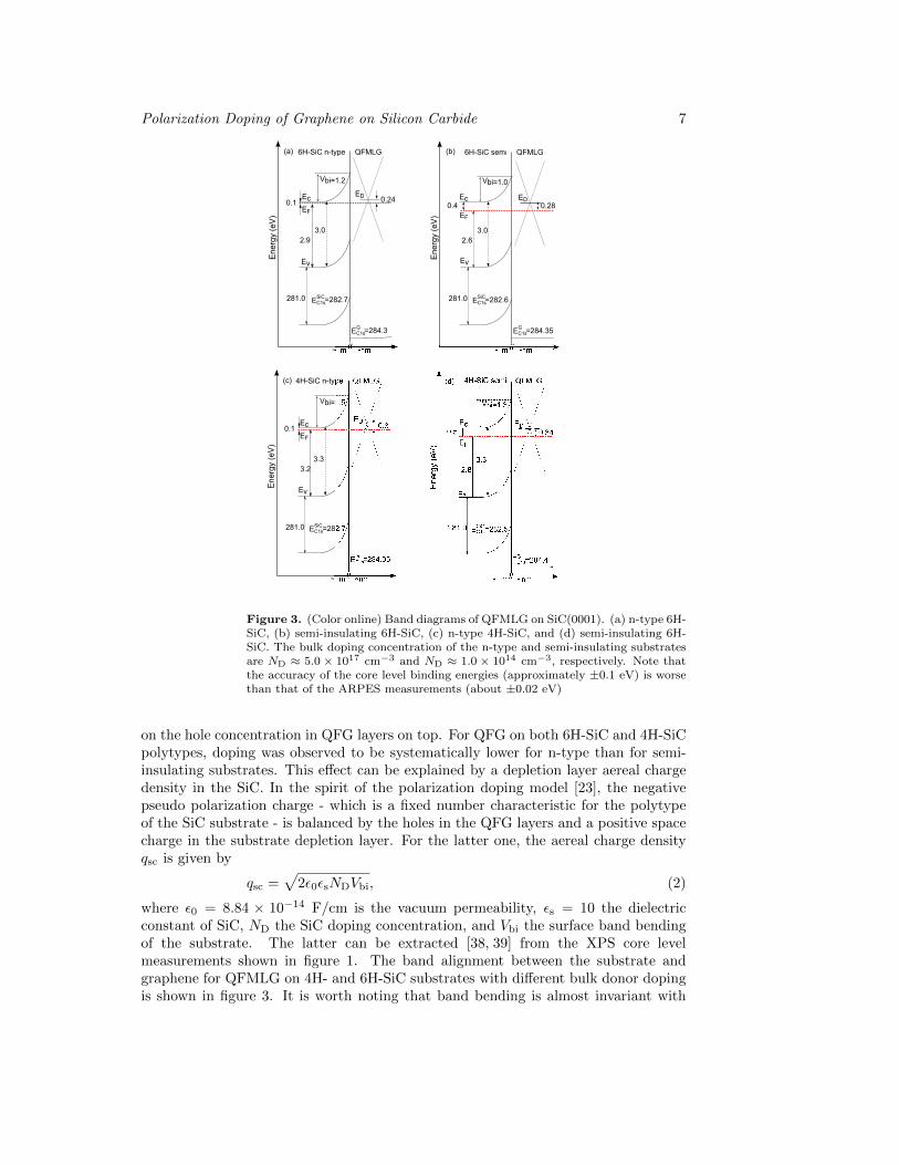
Figure 3. (Color online) Band diagrams of QFMLG on SiC(0001). (a) n-type 6H-SiC, (b) semi-insulating 6H-SiC, (c) n-type 4H-SiC, and (d) semi-insulating 6H-SiC. The bulk doping concentration of the n-type and semi-insulating substratesare ND ≈ 5.0 × 1017 cm−3 and ND ≈ 1.0 × 1014 cm−3, respectively. Note thatthe accuracy of the core level binding energies (approximately ±0.1 eV) is worsethan that of the ARPES measurements (about ±0.02 eV)
on the hole concentration in QFG layers on top. For QFG on both 6H-SiC and 4H-SiCpolytypes, doping was observed to be systematically lower for n-type than for semi-insulating substrates. This effect can be explained by a depletion layer aereal chargedensity in the SiC. In the spirit of the polarization doping model [23], the negativepseudo polarization charge - which is a fixed number characteristic for the polytypeof the SiC substrate - is balanced by the holes in the QFG layers and a positive spacecharge in the substrate depletion layer. For the latter one, the aereal charge densityqsc is given by
qsc =√
2ε0εsNDVbi, (2)
where ε0 = 8.84 × 10⁻¹⁴ F/cm is the vacuum permeability, εs = 10 the dielectricconstant of SiC, ND the SiC doping concentration, and Vbi the surface band bendingof the substrate. The latter can be extracted [38, 39] from the XPS core levelmeasurements shown in figure 1. The band alignment between the substrate andgraphene for QFMLG on 4H- and 6H-SiC substrates with different bulk donor dopingis shown in figure 3. It is worth noting that band bending is almost invariant with
Polarization Doping of Graphene on Silicon Carbide 8
addition of extra layers, thus calculations below are true for multilayer systems aswell.
By substituting the parameters into equation 2 one obtains qsc = 2.5×1012 cm−2
for QFG on n-type 6H-SiC(0001)with ND = 5.0×1017 cm−3 and qsc = 2.0×1010 cm−2
for semi-insulating 6H-SiC with ND = 1.0 × 1014 cm−3. Using the same formulawe obtain qsc = 2.8 × 1012 cm−2 for QFG on n-type 4H-SiC(0001)with ND =5.0 × 1017 cm−3 and qsc = 2.0 × 1010 cm−2 for semi-insulating 4H-SiC with ND =1.0 × 1014 cm−3. One should note that the number for bulk carrier concentrationcontains a rather large uncertainty (1.0×1017 cm−3 ≤ ND ≤ 1.0×1018 cm−3 for n-typesamples). Whereas qsc is negligible for the semi-insulating substrates, its magnitudefor the n-type case is within the uncertainty we have conceded consistent with thedifference of around 2.0× 1012 cm−2 in the aereal hole density of semi-insulating andn-type SiC substrates (see last column in Table 1). The electron transfer due to thedepletion of the n-type 3C-SiC substrate also naturally explains the n-type doping ofthe QFMLG layer on that substrate.
4. Conclusions
Multilayer epitaxial graphene (EG) and quasi-freestanding graphene (QFG) on the Si-face of three different polytypes of SiC was investigated by XPS and ARPES. The holeconcentration was observed to depend in a characteristic manner on the SiC polytypeas predicted by the polarization doping model [23]. 4H-SiC, which has the largestspontaneous polarization induces the largest carrier concentration in QFG, followedby 6H-SiC whose polarization and induced hole concentration are approximately 1.5times smaller. 3C-SiC, which has no spontaneous polarization, induces a negligiblen-type doping in QFG which is presumably due to bulk doping, i.e. the depletion ofthe n-type SiC substrate. The experiments provide strong evidence in favor of thepolarization doping model [23]. The model also provides a roadmap for the choiceof substrates for QFG. Clearly, 3C-SiC would be the substrate material of choicebecause it allows the lowest charge carrier concentration. On the other hand it wasshown previously that the deposition parameters for the growth of dielectrics canbe tuned to vary surface transfer doping of graphene [40]. This together with thepolytype-dependent polarization doping could provide a basis for tuning the chargecarrier concentration in QFG on hexagonal SiC polytypes.
The effect of polarization doping as well as bulk doping on graphene overlayernaturally takes place not only for QFG, but also for EG on SiC. In that case,the magnitude of this effect is apparently overcompensated by charge transfer frominterface states such as, e.g., dangling bonds.
Finally it is worth noting that polarization doping should also be considered forgraphene and other 2D materials on pyroelectric substrates. In conjunction withpiezoelectric substrates, where the polarization is changed by external forces, thiseffect could lead to novel applications in electronic devices.
5. Acknowledgements
The authors are grateful to Karsten Horn, Hendrik Vita and Stefan Bottcher from theFritz-Haber-Institute for their ongoing support during beam times at BESSY II as wellas for fruitful discussions. The research leading to these results has received fundingfrom the European Union Seventh Framework Programme under grant agreement
Polarization Doping of Graphene on Silicon Carbide 9
n◦604391 Graphene Flagship, from the DFG within the Collaborative Research CentreSFB 953 Synthetic Carbon Allotropes and within the Priority Programme SPP 1459Graphene (SE 1087/10-1), as well as from the European Science Foundation underthe EUROCORES Programme EuroGraphene (SE 1087/9-1).
References
[1] C. Berger, Z.M. Song, X.B. Li, X.S. Wu, N. Brown, C. Naud, D. Mayo, T.B. Li, J. Hass, A.N.Marchenkov, E.H. Conrad, P.N. First, W.A. de Heer, Science 312, 1191 (2006)
[2] K.V. Emtsev, A. Bostwick, K. Horn, J. Jobst, G.L. Kellogg, L. Ley, J.L. McChesney, T. Ohta,S.A. Reshanov, J. Roehrl, E. Rotenberg, A.K. Schmid, D. Waldmann, H.B. Weber, T. Seyller,Nat. Mater. 8, 203 (2009)
[3] P.N. First, W.A. de Heer, T. Seyller, C. Berger, J.A. Stroscio, J.S. Moon, MRS Bulletin 35, 296(2010)
[4] J. Moon, D. Curtis, M. Hu, D. Wong, C. McGuire, P. Campbell, G. Jernigan, J. Tedesco,B. VanMil, R. Myers-Ward, C. Eddy, D. Gaskill, IEEE Electron Device Lett. 30, 650 (2009)
[5] Y.-M. Lin, C. Dimitrakopoulos, K. A. Jenkins, D. B. Farmer, H.-Y. Chiu, A. Grill, and P.Avouris, Science 327, 662 (2010)
[6] Y. Wu, K. A. Jenkins, A. Valdes-Garcia, D. B. Farmer, Y. Zhu, A. A. Bol, C. Dimitrakopoulos,W. Zhu, F. Xia, P. Avouris, Y.-M. Lin, Nano Lett. 12, 3062 (2012)
[7] Y. M. Lin, A. Valdes-Garcia, S. J. Han, D. B. Farmer, I. Meric, Y. N. Sun, Y. Q. Wu, C.Dimitrakopoulos, A. Grill, P. Avouris, K. A. Jenkins, Science 332, 1294 (2011)
[8] A. Tzalenchuk, S. Lara-Avila, A. Kalaboukhov, S. Paolillo, M. Syvajarvi, R. Yakimova, O.Kazakova, T. Janssen, V. Falko, S. Kubatkin, Nat. Nanotechnol. 5, 186 (2010)
[9] K. V. Emtsev, F. Speck, Th. Seyller, L. Ley, J. D. Riley. Phys. Rev. B 77, 155303 (2008)[10] T. Ohta, A. Bostwick, J. McChesney, T. Seyller, K. Horn, E. Rotenberg, Phys. Rev. Lett. 98,
206802 (2007)[11] A. Mattausch, O. Pankratov, Phys. Rev. Lett. 99, 076802 (2007)[12] F. Varchon, R. Feng, J. Hass, X. Li, B.N. Nguyen, C. Naud, P. Mallet, J.Y. Veuillen, C. Berger,
E. Conrad, L. Magaud, Phys. Rev. Lett 99, 126805 (2007)[13] S. Goler, C. Coletti, V. Piazza, P. Pingue, F. Colangelo, V. Pellegrini, K. V. Emtsev, S. Forti,
U. Starke, F. Beltram, S. Heun, Carbon 51, 249-254 (2103)[14] S. Kopylov, A. Tzalenchuk, S. Kubatkin, and V. I. Falko, Appl. Phys. lett 97, 112109 (2010)[15] C. Riedl, C. Coletti, T. Iwasaki, A. A. Zakharov, U. Starke, Phys. Rev. Lett. 103, 246804 (2010)[16] C. Riedl, C. Coletti, T. Iwasaki, U. Starke, Mater. Sci. Forum 645-648, 623 (2010)[17] F. Speck, M. Ostler, J. Rohrl, J. Jobst, D. Waldmann, M. Hundhausen, H. Weber, T. Seyller,
Mater. Sci. Forum 645-648, 629 (2010)[18] F. Speck, J. Jobst, F. Fromm, M. Ostler, D. Waldmann, M. Hundhausen, H. B. Weber, Th.
Seyller, Appl. Phys. Lett. 99, 12216 (2011)[19] C. Virojanadara, R. Yakimova, A. A. Zakharov, L. I. Johansson, J. Phys. D: Appl. Phys. 43
374010 (2010)[20] C. Virojanadara, A. A. Zakharov, R. Yakimova, L. I. Johansson, Surf. Sci. 604, L4 (2010)[21] H. Tsuchida, I. Kamata, and K. Izumi, Jpn. J. Appl. Phys. Part 2 36, L699 (1997)[22] N. Sieber, B.F. Mantel, T. Seyller, J. Ristein, L.Ley, T. Heller, D.R. Batchelor, D. Schmeißer,
Appl. Phys. Lett. 78, 1216 (2001)[23] J. Ristein, S. Mammadov, and Th. Seyller. Phys. Rev. Lett. 108, 246104 (2012)[24] S. B. Austerman, D. A. Berlincour, and H. H. A. Krueger, J. Appl. Phys. 34, 339 (1963)[25] E. Loh, Phys. Rev. 166, 673 (1968)[26] Elastic, Piezoelectric and Related Constants of Crystals, O. Madelung (ed.), Landolt-Bornstein
Series, Vol III (Springer, Berlin, 1979)[27] M. Posternak, A. Baldereschi, A. Catellani, and R. Resta, Phys. Rev. Lett. 64, 1777 (1990)[28] R. Resta, M. Posternak, A. Baldereschi, and A. Catellani, Ferroelectrics 111, 15 (1990)[29] A. Qteish, V. Heine, and R. J. Needs, Phys. Rev. B 45, 6376 (1992).[30] J. Soltys, J. Piechota, M. Lopuszynski and S. Krukowski, New J. Phys. 12, 043024 (2010)[31] M. Ostler, F. Speck, M. Gick, Th. Seyller, Phys. Stat. Sol. B 247, 2924 (2010)[32] T. Ohta, A. Bostwick, T. Seyller, K. Horn, E. Rotenberg, Science 313, 951 (2006)[33] E. McCann, V.I. Fal’ko, Phys. Rev. Lett. 96, 086805 (2006)[34] S. Ulstrup, J. C. Johannsen, F. Cilento, J. A. Miwa, A. Crepaldi, M. Zacchigna, C. Cacho, R.
Chapman, E. Springate, S. Mammadov, F. Fromm, C. Raidel, Th. Seyller, F. Parmigiani, M.Grioni, P. D. C. King, Ph. Hofmann, Phys. Rev. Lett. 112, 257401 (2014)

Polarization Doping of Graphene on Silicon Carbide 10
[35] I. Gierz, J. Henk, H. Hochst, C. R. Ast, K. Kern, Phys. Rev. B 83, 121408 (2011)[36] Y. Liu, G. Bian, T. Miller, and T.-C. Chiang, Phys. Rev. Lett.107, 166803 (2011)[37] C. Coletti, K. V. Emtsev, A. A. Zakharov, T. Ouisse, D. Chaussende, U. Starke, Appl. Phys.
Lett. 99, 081904 (2011)[38] Th. Seyller, J. Phys.: Condens. Matter 16, S1755 (2004)[39] Th. Seyller, K. V. Emtsev, F. Speck, K.-Y. Gao, L. Ley, Mater. Sci. Forum 556-557, 701 (2007)[40] P. Wehrfritz, F. Fromm, S. Malzer, Th. Seyller, J. Phys. D: Appl. Phys. 47, 305103 (2014)