this document is downloaded from cityu institutional...
TRANSCRIPT

This document is downloaded from CityU Institutional Repository,
Run Run Shaw Library, City University of Hong Kong.
Title A driver design for retrofit LED lamp
Author(s) Gao, Jiabei (高加貝)
Citation Gao, J. B. (2011). A driver design for retrofit LED lamp (Outstanding Academic Papers by Students (OAPS)). Retrieved from City University of Hong Kong, CityU Institutional Repository.
Issue Date 2011
URL http://hdl.handle.net/2031/6319
Rights This work is protected by copyright. Reproduction or distribution of the work in any format is prohibited without written permission of the copyright owner. Access is unrestricted.

1
Department of Electronic Engineering
Final Year Project (FYP)
PROJECT REPORT
Bachelor of Engineering (Honors) in
Electronic and Communication Engineering
BEngECE – 2010/2011 – HC – 07
A Driver Design for Retrofit LED Lamp
Student ID Number:
Student Name: Gao Jiabei
Project Supervisor: Prof. Henry Chung
Project Assessor: Prof. Ron Hui

2
Student Final Year Project Declaration
I have read the student handbook and I understand the meaning of academic dishonesty, in
particular plagiarism and collusion. I declare that the work submitted for the final year project
does not involve academic dishonesty. I give permission for my final year project work to be
electronically scanned and if found to involve academic dishonesty, I am aware of the
consequences as stated in the Student Handbook.
Project Title: A Driver Design for Retrofit LED Lamp
Student Name: Gao Jiabei Student ID:
Signature: 高加贝 Date: 11 April 2011
No part of this report may be reproduced, stored in a retrieval system, or transcribed in any
form or by any means – electronic, mechanical, photocopying, recording or otherwise –
without the prior written permission of City University of Hong Kong.

3
Acknowledgement
This project would have not been possible without the extraordinary support of a number of
people. Firstly, I would like to send a huge ―thank-you‖ to my project supervisor Prof. Henry
Chung. He has been so kind and encouraging to FYP research projects since I approached to
him and showed my interests in Power Electronics in Semester A, 2009/10. Throughout my
final year study, I also learned theories about Power Electronics in a course taught by him.
I want to express as well my gratitude to my project assessor Professor Ron Hui, for providing
very useful comments and time in monitoring my progress.
Several Ph.D candidates in the Power Electronics Lab, Mr. Chen Nan, Miss. Karen Zhang and
Mr. Wang Huai took much of their time to help me with my FYP. Many useful technical
advices were generated and donated from their own research experiences and previous
research projects. Without their altruistic help, I will not able to finish my project on time.
Last but not least, I would like to thank Department of Electronic Engineering, for providing
so many academic and research opportunities for me to explore the world of engineering
within the recent three years. Clearly, as the most sophisticated, challenging and meaningful
research project I have done in my college, my FYP is the culmination of my study in
electronic engineering. This research experience will be an unforgettable one in my life.

4
Table of Content
Abstract ……………………………………………………………………………………… 7
Chapter 1 Introduction
1.1 Background ………………………………………………………………………. 8
1.2 Motivation ……………………………………………………………………….. 9
1.3 Objectives ……………………………………………………………………….. 10
Chapter 2 Literature Review
2.1 Basic Knowledge about LED …………………………………………………… 11
2.2 LED Driver Designs …………………………………………………………….. 13
2.3 Working Principles of Electronic Ballast ……………………………………….. 14
2.4 Power Factor Correction (PFC) Circuit ………………………………………… 22
2.5 AC-to-DC Rectifier ……………………………………………………………... 24
2.6 AC Power ……………………………………………………………………..… 25
2.7 Dimming Control Methods …………………………………………………...….32
2.8 Total Harmonic Distortion (THD) …………………………………………….... 37
2.9 Crest Factor (CF) ………………….……………………………………………. 38
2.10 Summary of Chapter …………………………………………………...……… 38
Chapter 3 Design Procedures
3.1 Introduction ………………………………………………………………………40
3.2 Circuit Modeling ………………………………………………………………... 40
3.3 Mathematical Modeling ……………………………………………………...…. 46
3.4 Limitation Analysis ……………………………………………………………... 48
3.5 Summary of Chapter ……………………………………………………………. 48
Chapter 4 Simulation Results
4.1 Introduction ……………………………………………………………………... 54
4.2 Simulation of Electronic Ballast ………………………………………………... 54
4.3 Simulation of PFC Circuit - Electronic Ballast …………………………………. 59
4.4 Simulation of Electronic Ballast - LED Driver …………………………………. 60
4.5 Simulation of PFC Circuit - Electronic Ballast - LED Driver ………………….. 64
Chapter 5 Experimental Result …………………………………………………………... 66
Chapter 6 Conclusion and Future Development ……………………………………...…. 71

5
List of Figures:
Figure 1: Typical LED Drivers in the market (all embedded in LED bulbs and lamps)
Figure 2: LED Driver in the Market vs. Proposed LED Driver Design for Electronic Ballast
Figure 3: Block Diagram of Typical Electronic Ballast
Figure 4: Anatomy of Electronic Ballast
Figure 5: Half-Bridge Resonant Inverter Electronic Ballast
Figure 6: Switching Patter of Half-Bridge Resonant Inverter Electronic Ballast
Figure 7: Buck-Converter Electronic Ballast
Figure 8: Voltage Output of the Switch and Current Input for the Inverter
Figure 9: Typical Circuit Schematic of Active PFC circuit
Figure 10: A Typical Rectifier Circuit and the Resulting DC Voltage Waveform with Ripples
Figure 11: Phasor Representation of Power
Figure 12: Relationship between Luminous Flux (%) and Forward Current
Figure 13: Dominating Wavelength vs. Current
Figure 14: V-I Relationship of LED Lamp
Figure 15: Active/ Reactive Power Flow
Figure 16: Circuit Modeling of LED Driver
Figure 17: Portion of Output Power and Absorption of Power by Adjusting the Phase
Figure 18: Equivalent Circuit of the Ballast and Fluorescent Lamp Model
Figure 19: Replacement of LED Driver and LED Unit
Figure 20: Circuit Diagram of LED Driver
Figure 21: Circuit Diagram of Electronic Ballast - LED Driver
Figure 22: Thevenin Circuit Equivalent of Ballast-Driver
Figure 23: Circuit of Buck-Converter Electronic Ballast
Figure 24: Circuit of Half-Bridge Inverter Electronic Ballast
Figure 25, 26 & 27: Output of Simulated Electronic Ballast

6
Figure 28: Pulsating Current at the Input Port
Figure 29: High-frequency AC, Low-frequency AC and Pulsating Current
Figure 30: Electronic Ballast with PFC module
Figure 31: Waveform of Vin and Iin, in phase, high pf
Figure 32 (a): Electronic Ballast – LED Driver with phase adjustment module
Figure 33: Phase shift = x degree, Vled = yV
Figure 34: Final Circuit Diagram of the Electronic Ballast – LED Driver
Figure 35: Analysis of Waveforms Vled, Vac1, Vac2, Vout and vo (25 degrees shift)
Figure 36: Phase Shift Analysis (25 degrees shift from Vac2 and vo)
Figure 37: Phase Shift Analysis (90 degrees shift from Vac2 and vo)
Figure 38: Laboratory Equipments for Final Year Project
Figure 39: DC Module Used for MCU
Figure 40: LED Units Working at Rated Voltage 27V
Figure 41: LED Unit Composed of Small LED Grid (Left)
Figure 42: LED Unit Working under Pure Diode Bridge Rectifier
Figure 43: LED Unit Working under MCU Controlled Dimming Control Mode
Figure 44: Circuit Diagram of LED Driver
List of Tables:
Table 1: Trend of Development of Key Properties of LED Lamp from 2008 – 2015
Table 2: Comparison of Categories of Electronic Ballast
Table 3: Three Working Stages for Electronic Ballast
Table 4: Advantages of PWM Dimming Control Method
Table 5: Phase Shift between V and I and Decrease of Active Power (Straight Line)
7
Abstract
LED lamp tubes are becoming more and more popular in recent light fixture market,
especially fluorescent lamp tube replacement market. To replace a LED lamp tube directly
with fluorescent lamp tube, a special design for LED driver compatible with the supply
sources output by electronic ballast needs to be proposed. In this project, under the guidance
of Professor Henry Chung and the help of his research group in Power Lab of CityU, a design
of LED driver which can be embedded in LED lamp tube that can operate with electronic
ballasts without rewiring the existing circuitry inside the fluorescent lamp holder is presented.
Another feature of this LED driver is the function of dimming control. The kernel technology
of this driver design to achieve the power conversion is the adjustment of the input impedance
of AC-to-DC converter. Through this adjustment, the active and reactive power drawn from
the electronic ballast to the LED lamp can be controlled. The concept of this retrofit design
allows convenient replacement of fluorescent lamps with LED lamp tubes without removal or
replacement of existing electronic ballasts. Once the prototype is commercialized and finally
becomes real product, the market potential will be huge, since customers who could afford
this kind of retrofit LED lamp must have used electronic ballasts before. A 20W retrofit LED
lamp prototype is built, and the performance of it is evaluated in this project.
8
Chapter 1 Introduction
1.1 Background
Fluorescent lamp tube has been widely used as light equipment, due to its advantages of
providing longer lifespan and less power consumption than an incandescent light does.
However, it might not be as energy-efficient as LED lamps today. On contrary, the leakage of
mercury from wasted fluorescent light has even become another source of pollution to the
environment. Therefore, the idea of replacing the fluorescent tube with LED was getting more
and more popular. Should this idea be realized, it will do help human society to save huge
amounts of energy and solve many environmental problems. However, realizing this
feasibility in practice is frustrated by a number of difficulties. Firstly, there will be
considerable labor costs involved in the installation, because people need to open the light
fixture to disassemble the existing ballast, either it be an electronic one, or a magnetic one.
Secondly, people might just throw away the removed ballasts. Clearly, it is not a desired
solution for fluorescent lamp replacement, because of the extra costs paid and lack of recycle
scheme of ballasts.
Instead of removing the existing electronic ballast for installation of LED lamp tubes, my
research presents a LED driver embedded in the naked LED lamp to allow a direct
replacement of fluorescent lamps. The proposed LED driver has a value-added function,
which is dimming control. The new type of LED lamp tube is called ―retrofit design of LED
lamp‖. Clearly, this solution outperforms the current method of fluorescent lamp replacement.

9
This project is aimed at designing the circuitries of a LED driver which could be geared on
electronic ballast for fluorescent lamp tubes. In order to drive the LED lamp in DC mode,
basic knowledge of power electronics, including AC-to-DC conversion, DC-to-AC
conversion (inverter) and PWM control, need to be used. The design procedures started from
an investigation on the performance of electronic ballast, and continued with a simulation
process by trial and error of the circuitries of half-bridge rectified, and finally ended with the
construction of the mathematical model of the circuit system and the solutions of the
parameters. The final design was consolidated on computer simulation and verified by
experimental result.
The software used for computer simulation in this project is PSim, which is recommended by
Professor Henry Chung and PhD candidates. This software is actually very popular in the
field of power electronics and electrical-mechanical control. PSim is capable of nearly all the
circuit simulation in power electronics, with a user-friendly interface, fast-computation speed,
high resolution and accuracy.
In some other procedures and discussions of this report, computer aid of Microsoft
Mathematics was used in the active/reactive power analysis.
1.2 Motivation
Current LED lamps in the market are incompatible with standardized lamp fixtures
that are originally designed for fluorescent lamps, needing labor costs to rewire
circuitries for installation.

10
LED lamps are flexible for dimming control, but dimming control function is not
usually used in current LED lamp tubes, because of inferior design of LED driver
1.3 Objectives
To study the basic knowledge of LED lamps and different categories of LED drivers
To study the working principles of electronic ballast
To investigate on the methods of dimming control
To use the principle of AC power engineering for the driver design
To compare different modes of LED driver and draw a conclusion

11
Chapter 2 Literature Review
2.1 Basic Knowledge about LED
A. Sources of Concerns
LED technology is an obvious area that we can achieve energy savings as well as economic
benefits in the next decade. Currently, LED technologies are successful in decorative, display,
signaling and signage sectors, but not so successful in general public lighting sector.
Compared with the traditional fluorescent lamps invented half a century ago, LEDs tend to
have longer life expectancy and higher resistant to vibration failure. They also consume less
power than all light equipment nowadays. Moreover, they contain no toxic elements, such as
mercury, and emit no ultra-violet light, which is harmful for human health. However, The
high cost (usually 10 times that of fluorescent tubes) of all kinds LED lamps is one factor that
deters general customers from using LED lamps, the incompatibility of electricity
infrastructures, including the AC electricity supply and the use of lamp ballast is another
important issue that resists the mass application of LED lamps.
B. A Promising Future
LED lamps have a promising future. All research interests about LED as daily lighting
sources saw an amazing development in the past five years, including electrical interfaces
(drivers, power management), mechanical interface (fixture design, housing and geometry of
LED grids), thermal interface (heat sink) and photometric interface (material science &
engineering). It is estimated that all key elements for research in this research area will be
12
improved steadily until the year 2015, when all standards of LED as lighting equipments
finally become mature and strictly regulated.
Table 1: Trend of Development of Key Properties of LED Lamp from 2008 - 2015
C. Economic Analysis of LED Lamp Applications
As estimated by China’s Bureau of Energy, 400 millions of new fluorescent lamps were
purchased in domestic market of China, and around 1 billion fluorescent lamps were used. If
it is assumed that on average 4 hours of running time per lamp and the power rating of LED
lamp is 25 Watts, then on average the power consumed is 0.1 KWh per day. With a rough
calculation, 30 billion KWh of electricity will be consumed per year. If LED lamp is assumed
to save half of the power consumed by fluorescent lamp, only 15 billion KWh of electricity
will be used. If we could add dimming control to LED lamps and we assume that around 10%
more electricity could be saved by it, 1.5 billion KWh more electricity will be saved again.
This is a considerable number, because if 0.7RMB/KWh, around 1 billion RMB (= 153
13
million US$) will be saved. We could reinvest this amount of money to investigate on more
efficient lighting equipments.
2.2 LED Driver Designs
In the market, LED lamp tubes and other LED light fixtures must be equipped with LED
drivers to function. Since LED lamp requires AC-to-DC conversion, (See section 2.4 for
Rectifier) an important electrical component plays a key role, which is the capacitor used for
smoothing the voltage. Normally electrolytic capacitor, which has lower cost, is massively
used in LED drivers. The figure (Figure 1) below displays four typical models of LED drivers.
Figure 1: Typical LED Drivers in the market (all embedded in LED bulbs and lamps)
It could be seen that components like transformers, capacitors, MOSFETs and diodes, which
are necessary components for rectifiers, are used in these drivers.
However, it is estimated that the electrolytic capacitor has only a lifespan of several thousand
hours. Therefore, the lifespan of the whole LED lamp (with driver) has a bottleneck in terms
of this electrolytic capacitor. The reason why electrolytic capacitors could pose a serious

14
degradation to the lifespan of LED lamp is because of the vaporization of the electrolytic
liquid inside due to the temperature rise in the circuit. Without an efficient and long-life
capacitor to achieve the smoothing effect of AC-to-DC conversion, advantage of LED lamp’s
longevity of working hours could not be revealed.
Figure 2: LED Lamp Tube Driver in the Market vs. Proposed LED Driver Design for
Electronic Ballast
Successful LED drivers could facilitate the energy-saving mission, since the power
consumption of the LED lamp is generally lower than that of the fluorescent lamp. In addition,
the proposed retrofit design of LED lamp could provide dimming function with users, which
means more energy-saving capacity.
2.3 Working Principles of Electronic Ballast:

15
Fluorescent lamp converts electrical power into useful light more efficiently than an
incandescent lamp. Lower energy cost typically offsets the higher initial cost of the lamp. In
the lamp fixture holding fluorescent lamp tubes, a kind of power conversion device, ballast,
needs to be added in order to regulate the current flowing through the lamp.
Electronic ballast, which functions at high-frequency to drive the fluorescent lamp, has been
widely used with fluorescent lighting systems for over 30 years. It tends to be more energy
efficient and runs more quietly than traditional magnetic ballasts. Compared with traditional
magnetic ballast, electronic ballast can reduce the flickering effects of the lamp and hence
creates a comfortable light output to human eyes.
A. Advantages of Electronic Ballast
Higher power efficiency
High frequency mode, no obvious flickering effect
Less noisy, no buzzing sound
Easy to achieve dimming control
Extending the lifespan of fluorescent lamp
Easy for implementation of PFC circuit (see Section 2.4)
High input power factor (pf)
Low input current total harmonic distortion (THD)
Good lamp current crest factor (CF) (see Section 2.9 – 2.10)
Lighter weight and smaller size

16
However, there are some disadvantages of using electronic ballasts. Firstly, electronic ballast
tends to be more reliable than magnetic ballast, but its burn-out rate are on average higher
than its magnetic counterpart. Secondly, once a lamp ballast has burned out, the only way to
save is to replace it by a new one. Thirdly, since electronic ballasts work at very high
frequencies (20 – 60 KHz), they can create radio frequency noise and electromagnetic
interferences to power lines and indoor ambience. However, these issues belong to general
education, and will not be discussed in this report.
B. Categories of Electronic Ballast
Category A Category B
Independent electronic ballast Embedded electronic ballast CFL
Ballast with pre-heat stage Ballast without pre-heating stage
Ballast with PFC circuit Ballast without PFC circuit
Ballast with dimming control function Ballast without dimming control function
Table 2: Comparison of Categories of Electronic Ballast
C. Circuit Design of Electronic Ballast
Figure 3 shows the block diagram of typical electronic ballast. It is constituted with two
power-conversion process (AC-to-DC) and (DC-to-AC). The final effect is a frequency
increase from 50Hz (low) to tens of KHz (high)
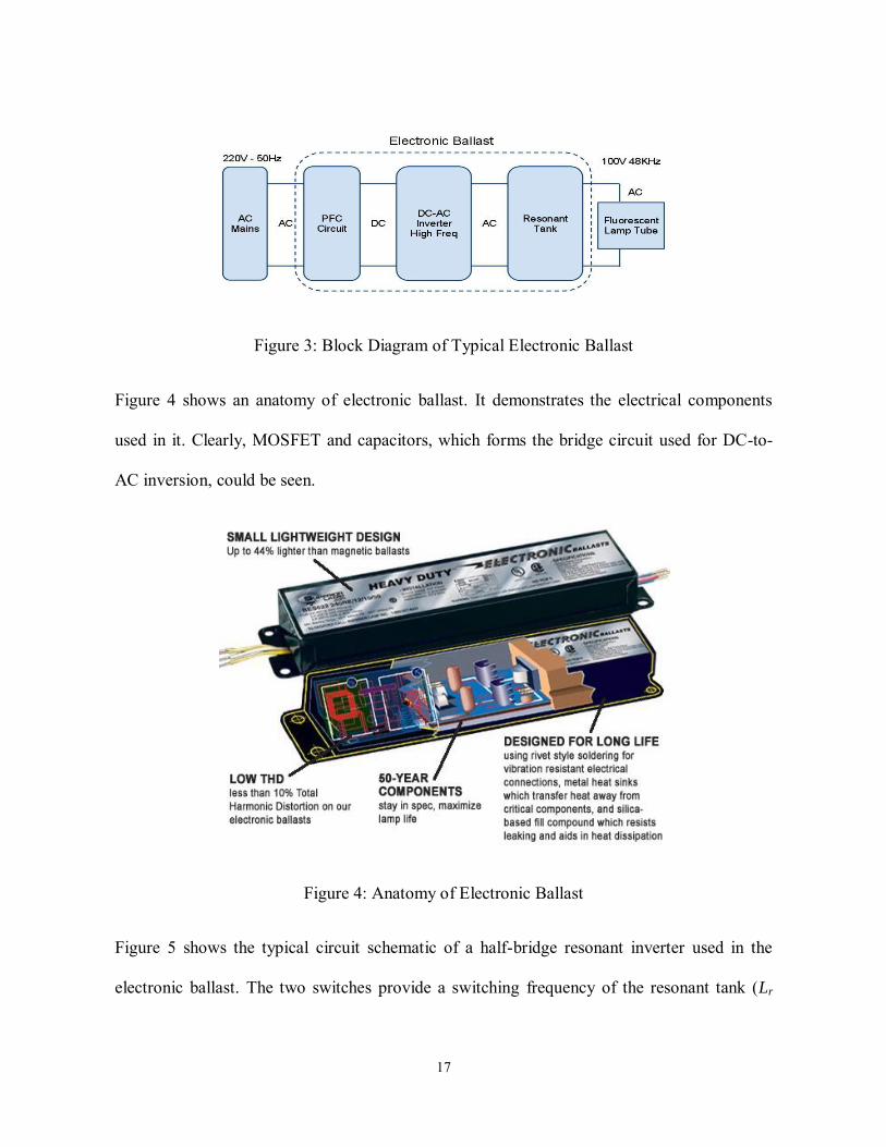
17
Figure 3: Block Diagram of Typical Electronic Ballast
Figure 4 shows an anatomy of electronic ballast. It demonstrates the electrical components
used in it. Clearly, MOSFET and capacitors, which forms the bridge circuit used for DC-to-
AC inversion, could be seen.
Figure 4: Anatomy of Electronic Ballast
Figure 5 shows the typical circuit schematic of a half-bridge resonant inverter used in the
electronic ballast. The two switches provide a switching frequency of the resonant tank (Lr

18
and Cr). This electronic ballast circuit could drive two fluorescent lamps at the same time. The
half bridge working schematics could be explained by Figure 6.
Figure 5: Half-Bridge Resonant Inverter Electronic Ballast
Figure 6: Switching Patter of Half-Bridge Resonant Inverter Electronic Ballast
In Figure 6 (a), the switch of VT1 is on and VT2 is off, thus creating a circuit as shown by the
arrow in (a). In Figure 6 (b), the switch of VT2 is on and VT1 is off, thus creating a reversed
circuit as shown in (b). Note that the LCRL network consists of two identical resonant tanks in
Figure 7. Also note that the current flowing through RL (fluorescent lamp) is in a reversed
direction in (a) and (b). Therefore, with a high frequency switching, a sinusoidal AC with
high frequency (20 – 60 KHz) could be formed with the LCRL network.

19
Figure 7 is another typical design of electronic ballast. It is in fact a two-switched buck
converter. Vg is a DC and Vxy before the capacitor C is a PWM chopped DC. With the
function of a DC-isolation capacitor C, the DC component is filtered out, leaving with an AC
square wave Vxy. After the LCR filter, which is similar to the one shown in Figure…, a high-
frequency AC wave is created at rFl.
Figure 7: Buck-Converter Electronic Ballast
There are in total three working stages for electronic ballast as shown in Table 3:
Stage Description
Pre-heat Stage: In this stage, the lamp is non-conducting, with a high equivalent resistance value. The switching frequency of S1 and S2 are set at a higher value than the natural frequency of LrCrrF1 network, in order to pre-heat the filaments.
Ignition Stage: In this stage, the switching frequency is decreased toward the resonant frequency at which the Vlamp and lamp power is at the rated value.
Steady Stage: With the ignition of fluorescent lamp, the temperature of the filaments increased, causing rFl to decrease. The lamp voltage is decreased as proportionally.
Table 3: Three Working Stages for Electronic Ballast
20
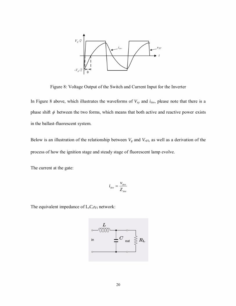
Figure 8: Voltage Output of the Switch and Current Input for the Inverter
In Figure 8 above, which illustrates the waveforms of Vxy and iinv, please note that there is a
phase shift between the two forms, which means that both active and reactive power exists
in the ballast-fluorescent system.
Below is an illustration of the relationship between Vg and VrFl, as well as a derivation of the
process of how the ignition stage and steady stage of fluorescent lamp evolve.
The current at the gate:
inv
invinv
Z
vi
The equivalent impedance of LrCrrFl network:

21
Flr
Flr
r
Flr
r
Fl
rFlCrLrinvrCj
rLj
Cj
rCj
Cj
r
LjrZZZ
11//
Therefore:
FlFlrrr
Flrinv
rrCLLj
rCjZ
21 1
The magnitude of iinv is:
2222
222
)(1
FlrrFlr
Flrinvinv
rCLrL
rCvi
LCf
21
0 , LC
10
Using voltage divider:
inv
rFlrrFl
Flinv
Flr
Flr
Flr
Fl
r VLjrCLr
rV
rCj
rLj
rCj
r
VFl
2
1
1
At resonant frequency,
inv
r
rFlinv
r
r
Fl
inv
rFlrrFl
Fl
r VL
CjrV
C
Lj
rV
LjrCLr
rV
Fl
2

22
After the fluorescent lamp is ignited with a higher voltage than Vinv, the fluorescent lamp goes
into steady-state, in which rFl becomes smaller. Since VrFl is proportional to the value of rFl,
then the VrFl will also decrease. This change confirms the descriptions in Table 3.
2.4 Power Factor Correction Circuit
Power Factor pf is an important gauge in AC power system. Please see section 2.6 AC Power
for explanations in detail. The cause of low pf is due to the property of rectification process
explained in Section 2.5. They ―polluted‖ the public electricity transmission system
extraordinarily, but they are still massively used, because of their simplicity in structure and
low cost. Without PFC circuit, a single device connected to the AC mains might not be
revealed clearly. But if millions of such devices that have no PFC regulation, the high-
frequency harmonics contained in the pulsating current might ―pollute‖ the whole electricity
transmission system in a large extent.
Excessive current harmonic components might cause more power consumption and heat for
electrical engines and generators with contains coils. It might also break down the electronic
ballast. When it comes to the worst case, it might also lead to burnt-down and fire, and huge
amounts of economic losses. Therefore, from perspectives of protecting the electrical system
as well as protecting human safety, current harmonics must be reduced as much as possible.

23
Problems of having no PFC circuit:
Sharp and high current pulse, around 10-20 times of current in steady-state
Narrow conduction angle, THD (Please see section 2.8) will even reach 100%
In this section, Power Factor Correction (PFC) circuits that are typically used in driving
circuits will be introduced. The basic working principle of PFC circuit is to force the pulsating
current to follow the phase pattern of voltage, by using a control circuit. Achieving a
sinusoidal current with a phase synchronization of sinusoidal voltage, PFC circuit could be
seen as a purely resistive component in the circuit. Figure 9 is a circuit schematic of Active
PFC circuit.
Figure 9: Typical Circuit Schematic of Active PFC circuit
For analysis of PFC circuit, please see Section 4 for simulation results. Since there are
embedded PFC implementation in the commercialized electronic ballast, PFC is not
considered in the performance analysis of the circuit.

24
2.5 AC-to-DC Rectifier
A rectifier is a device that converts AC voltage to DC voltage, through a process known as
rectification. A device which performs the opposite function (DC-to-AC) is known as an
inverter. This figure (Figure 10) below shows a typical rectification process:
Figure 10: A Typical Rectifier Circuit and the Resulting DC Voltage Waveform with Ripples
Using diode-bridge only, structures of rectifier can only produce a pulsating DC output, but
not a constant-voltage DC. In order to produce steady DC, a smoothing circuit must be used.
Hence, a smoothing capacitor, which is placed right in parallel with the diode-bridge, can be
used to filter out the ripples. Therefore, this capacitor can also be regarded as a low-pass filter,
which filters out the high frequency components of AC ripples and preserves the low
frequency component of DC. However, there will still be some AC ripples left, caused by the
charging-discharging effect of the smoothing capacitor.

25
2.6 AC Power
In alternating current (AC) circuits, energy storage elements such as inductance and
capacitance may result in periodic energy exchange between them inside the circuit and
electrical system. The part of power that results in a net transfer of energy in one direction (to
be consumed by electrical/electronic devices) over a complete cycle of the AC waveform, is
called real power, while the portion of power, which was stored in capacitors and inductors
and returns to the source over each complete AC cycle, is known as reactive power.
If the load device is purely resistive (R), the sinusoidal current (I) and voltage (V) flowing
through it and over it are in phase at the same time. In other words, at every instant the
product of I and V is positive, meaning that the direction of energy flow is unique (the load is
consuming electrical power to do other jobs). Using similar analysis of the sinusoidal V and I
and phasor representation of C and L, if the load is purely reactive, then the energy flows
toward the load (consumed by the load) is equal to the energy that flows back (to the source).
There is no net energy flow over one cycle. In this case, only reactive energy flows—there is
no net transfer of energy to the load.
A. Instantaneous Power:
In real world, loads might have resistance, inductance, and capacitance elements, so both real
and reactive power need to be considered. Instantaneous power is a measure of power flow
over time:
)cos()cos()()()( ivmm ttIVtitvtp

26
Here, mV is the peak value of sinusoidal voltage and iV is the peak value of sinusoidal current.
v is the phase of sinusoidal voltage and i is the phase of sinusoidal current.
After trigonometry arrangement
)2cos(21)-cos(
21)( i ivmmvmm tIVIVtp
Thus, instantaneous power has a DC component and an AC component. DC component is a
constant value of:
)-cos(21
ivmm IV
And the AC component is a cosine function with peak value:
mm IV21
Using the theory above, if p(t) is larger than 0, it means that the power is absorbed (consumed)
by the load, while if p(t) is smaller than 0, it means that the power is absorbed (consumed) by
the source. Below is an example of instantaneous power illustration, using the simulation
software of Microsoft Mathematics.

27
It could be noticed that, the blue line is function 1 (voltage), the green line is function 2
(current). Function 3 is the pink line, which is the product of function 1 and 2, which
represents the instantaneous power. Function 4 is the DC component, whose value is:
)-cos(21
ivmm IV.
B. Average Power:
It measures the average value of instantaneous power over one complete cycle period.
)-cos(21)(
T1P i
T
0avg vmm IVdttp , which is the DC component of the instantaneous
power. Clearly, the sinusoidal part of the instantaneous power averaged zero during one full
cycle.
C. RMS Values in AC Power Analysis:

28
Equating the two identities:
T
dttiT
RRdtti
TP
0
2T
0
2avg )()(1 and P = Ieff
2R, where R is the
resistance and i(t) is the AC current flowing through. rmseff IdttiT
I T
0
2)(1
The RMS (effective) of a periodic I or V is the DC I or V that deliver the same average power
to a resistor as the AC I or V.
If I and V are sinusoidal quantities, the RMS value of them are:
2I m
rms
I and
2m
rms
VV
Hence, avgP )-cos( ivrmsrms IV
D. Apparent Power:
The quantity S is defined as apparent power. It is a measure in volt-amperes (VA) to
distinguish it from the unit used by average and real power.
rmsrms IVS
)cos( i vavg SP
Apparent power is a quantity that is cared about by engineers, because it is the real useful
power at the load, which is desired by users. However, components in the circuit such as
conductors and inductors must be designed to carry the total current, not just the current that
does useful work.
29
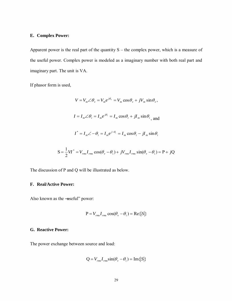
E. Complex Power:
Apparent power is the real part of the quantity S – the complex power, which is a measure of
the useful power. Complex power is modeled as a imaginary number with both real part and
imaginary part. The unit is VA.
If phasor form is used,
vmvm
j
mvm jVVeVVV v sincos ,
imim
j
mim jIIeIII i sincos , and
imim
j
mim jIIeIII i sincos*
QP)sin()cos(21S ii
* jIjVIVVI vrmsrmsvrmsrms
The discussion of P and Q will be illustrated as below.
F. Real/Active Power:
Also known as the ―useful‖ power:
}Re{)cos(P i SIV vrmsrms
G. Reactive Power:
The power exchange between source and load:
}Im{)(sinQ i SIV vrmsrms

30
The unit of reactive power is Var.
Hence, apparent power: 22 QS P
The relationship between complex power, real power and reactive power is shown in the
Figure 11 below, where Phase of Current (φ) is the phase difference between V and I:
i v
Figure 11: Phasor Representation of Power
Since reactive power in AC must be needed to support the transfer of real power over the
network. Therefore, we could not conclude that reactive power is not useful. In fact, it is very
useful so that the function of the circuit could be maintained.
H: Leading and Lagging:
Inductor stores energy in magnetic field, which consists of coil of wire. It takes time for I to
reach its peak value, when the V is added across the coil to build up a magnetic field. This
causes the value of I to lags the value of V. And we say that inductive devices ―absorb
reactive power‖. On the contrary, Capacitor stores energy in electric field. It takes time for

31
charge to build up to produce the full V. This causes the value of I to lead the value of V in
phase. And we say that capacitive devices ―generate reactive power‖.
I: Power Factor:
pf is a measure of the efficiency of a power system. If two power systems are transmitting the
same amount of real (active) power, the one with the lower pf will have higher circulating
currents due to energy that exchanges between source and load. It is the ratio between real
power and apparent power. In pure sinusoidal case, it is also the ration between Pavg and
apparent power.
cos)cos( ivS
Ppf
Consider a rectifier drawing some current waveform, and express
)sin()( tVtv s
0
)sin()(n
nn tniti
Real Power:
)()sin()sin(21
)sin()()sin(21)()()(
21
20
22
tdtntiV
tnitdtVtdtitVP
nns
n
nns
32
By orthogonality, all terms except for fundamental drop out, and the real power P is:
11
11
20
221
cos
cos2
)()sin()sin(21
)()sin()sin(21)()sin(
21
RMSRMS
snns
n
nnss
iV
iVtdtntiV
tdtnitVtdtiVP
So the only current component that contributes to active/real power is the fundamental
component in phase with the voltage.
kki
i
iV
iV
S
Ppf d
RMS
RMS
RMSRMS
RMSRMS
1
111 coscos
kd: distortion factor (<=1) shows how much the utilization of the source is reduced because of
harmonic currents that do not contribute to power (shape of the current);
kθ: displacement factor (<=1) shows how much utilization of the source is reduced due to
phase shift between the voltage and fundamental current (position of the current)
2.7 Dimming Control
A. Introduction
Ever since the greenhouse effect and global warming became a pressing issue internationally,
people are becoming more and more aware of the importance of cutting the electricity waste

33
when it is not needed. Lighting consumption is clearly a large portion of this cut, since it takes
around 20% of the global gross electricity consumption on average.
In fact, in many scenarios, light equipments need not to be run at full power as they are now.
For example, the street lamp during the mid-night, the fluorescent lamp in the sunny day in
schools, factories, hospitals etc., and the high-brightness lamp in the public parking lot. If
lamps could be dimmed down and up according to people’s real need, huge portion of energy
wasted could be saved.
Now, it is a great relief that LED lamps emerge in time, and it has some significant
advantages over the traditional lamps. It is also known that LED lamps, which use DC, rather
than AC, is flexible in dimming control. If we could use this flexibility fully and efficiently, it
will certainly become another aspect to save more energy.
Figure 12: Relationship between Luminous Flux (%) and Forward Current
The figure above shows the relationship between forward current of LED lamp and its relative
luminous flux (i.e. its strength of light output). So if we scale the light output at 350 mA as
100% full strength, then the light output at 200mA is around 60% and the light output at

34
100mA is 25%. Therefore, it is easy to achieve dimming control by adjusting the current
flowing through the LED.
Sample Light Strength Current I (mA)
1. 100% 350
2. 60% 200
3. 25% 100
B. Problems related to current adjustment:
Change of photometric properties of LED lamp
Figure 13: Dominating Wavelength vs. Current
However, although it seems straightforward that dimming control using current adjustment is
easy to achieve, there is a serious problem occurred to the photometric effect of LED lamp.
The figure above shows that the dominating wavelength emitted by the LED lamp will change
when the current changes:
Sample Dominating Wavelength (nm) Current I (mA)

35
1. 545.8 350
2. 548.6 200
3. 550.2 100
It is certain that this problem might not be a severe one in terms of real applications, but
people might not want that happen in some lighting systems or services with strict color
control. Since human eyes are very sensitive to the even a minor shift in light spectrum,
current adjustment control is not the most ideal method.
Change of current – change of voltage
Figure 14: V-I Relationship of LED Lamp
According to the V-I relationship of LED lamp, a current change (forward bias) through the
light emitting diode leads to a corresponding change of the voltage added on it, and vice versa.
That is to say, change of current will inevitably change the relationship between the voltage of
the source and the voltage of the load. With analysis of DC-to-DC conversion circuit, this

36
effect will cause an obvious flickering effect (low-frequency), which could be seen clearly by
users.
C. Other issues of current adjustment
Another issue of current adjustment is about heat effect. Heat caused by the LED driver
would not decrease with the decrease of current output to LED lamp. Due to decrease of the
efficiency of the LED driver with the reduction of current, the heat caused by the driver will
increase, if the light is dimmed down. It will even burn out the LED driver.
D. Dimming control using PWM
By changing current or voltage, the final goal is to control the power output to the LED lamp.
By using PWM control, constant current output to LED lamp could be dimmed. If a MOSFET
switch is added in series with the LED lamp, the power of LED lamp could be controlled.
There are several advantages of PWM dimming control:
Advantages Reasons
1. No shift of light spectrum for dominating wavelength
LED lamp is always working at 0-full current
2. High accuracy Power is proportion to duty cycle of the pulse wave
3. Digital control PWM signal could easily be generated by MCUs
4. No flickering effect V-I relationship of LED lamp would not be changed
Table 4: Advantages of PWM Dimming Control Method
However, the proposed method for dimming control used in this research is not PWM.

37
2.8 Total Harmonic Distortion
From Section 2.6 AC Power, it is known that power factor could be represented as:
cos)cos( ivS
Ppf
kki
i
iV
iV
S
Ppf d
RMS
RMS
RMSRMS
RMSRMS
1
111 coscos
Another measure of distortion in AC Power is total harmonic distortion (THD):
21
12
i
iTHD n n
THD is a measure of the RMS value of the rest of the harmonics normalized to the RMS of
the fundamental (square root of the power ration). Distortion factor could be used to represent
THD:
21
21
2
21
12
RMS
RMSRMSn n
i
ii
i
iTHD
211
THDkd
When V and I are in phase:

38
211)0cos(
THDkkkkpf ddd
2.9 Crest Factor
The crest factor is also called ―peak-to-average ratio (PAR)‖. It is a measurement of an AC
waveform, which is derived from the division of peak amplitude over the RMS value of the
waveform. Since RMS value is usually derived from peak value, we normally calculated the
CF by normalizing RMS value to be one.
2.10 Summary of Chapter
This chapter presents the keywords and understanding of them for the literature review in
preparation for the whole project about a new LED driver for a retrofit design of new LED
lamp tube. LED industry was briefly discussed and some of the reasons why LED lamp is
getting more and more accepted by customers are introduced. Then the important section of
LED driver is discussed. As one of the most important interfaces for LED lamp modules,
LED driver as electrical interface plays an important role in adapting the power from AC
mains to LEDs. Electronic Ballast, Power Factor Correction, AC-to-DC regulation
(rectification), and basic knowledge about filters are mentioned as well. Since this paper uses
the control of active/reactive power flow to achieve adaptation of electrical properties and
dimming control function, two sections about AC power and LED dimming control methods

39
are presented. In this chapter, complexities of problems and confinement for design criteria to
be met are discussed, which reveal that LED driver design is a science that requires prudent
thinking and careful engineering skills. This chapter forms the foundation of knowledge used
in this FYP, and concepts, equations and knowledge will be referred by subsequent chapters
of this report.

40
Chapter 3 Design Procedures
3.1 Introduction
In this chapter, the design method of the LED driver will be illustrated. Using the background
knowledge introduced and discussed in the previous chapter, the circuit model of the driver
will be shown. The design criteria is to use the timing of the switching MOSFET to control
the phase of the input current and voltage, thus changing the active/reactive power absorbed
by the LED lamp. In this process, LED lamp needs to be modeled as a complex component,
which consists of a purely resistive part and a reactive part. Without this premise, power could
not be exchanged between LED lamp and electronic ballast. Circuit structure will be proposed
for the LED lamp, through a re-consideration of the electronic ballast-lamp system. Finally, a
mirror structure will be proposed, and an equivalent circuit will be modeled, for convenience
of mathematical modeling. The final problem is the choice of values of two capacitors and
one inductor. Through mathematical modeling, the resonant tank will be designed and the
design is finished.
3.2 Circuit Modeling
The foremost issue to think about is that the LED lamp must function at a DC voltage.
Therefore, the whole circuit must be an AC-to-DC inverter circuit.
The second thought is about dimming control. Figure 15 shows a schematic of dimming
control of the electronic ballast-LED lamp system. If the active power flowing out of the

41
electronic ballast could be controlled, the brightness of the LED lamp could be controlled as
well. After some meditation and understanding of a massive amount of literature review, a
basic structure of the energy flow in this circuit is developed.
Figure 15: Active/ Reactive Power Flow
Figure 16: Circuit Modeling of LED Driver
Recall that the equation for active power and reactive power is:
}Re{)cos(P i SIV vrmsrms and }Im{)(sinQ i SIV vrmsrms

42
And for sinusoidal waveforms, 2
I mrms
I and
2m
rms
VV
In Figure 17 below, if the phase difference between vL’ and iL’ which are the voltage output
and current output at the electronic ballast could be modified by some certain scheme, the
active power (brightness of the lamp) could be controlled.
Figure 17: Portion of Output Power and Absorption of Power by Adjusting the Phase
With these two thoughts above, the implementation of such as LED driver could be realized
by a high-frequency half-bridge AC-to-DC inverter. The gate signals of the two MOSFET
could be synchronized with the lamp voltage vL’ with a phase difference , as shown in Figure
17 above.
43
We need a capacitor for DC isolation and another LC circuit to construct a filter that could
transform a square wave to a sinusoidal wave. It is important to use a capacitor for DC
isolation. Without DC isolation, transformer will be subject to a DC voltage, which is not
desirable, because this DC voltage will cause a saturation of current of the coil for the
transformer and finally burns the transformer. Another usage of this capacitor is to eliminate
the DC component in the sinusoidal waveform, which is always larger than zero.
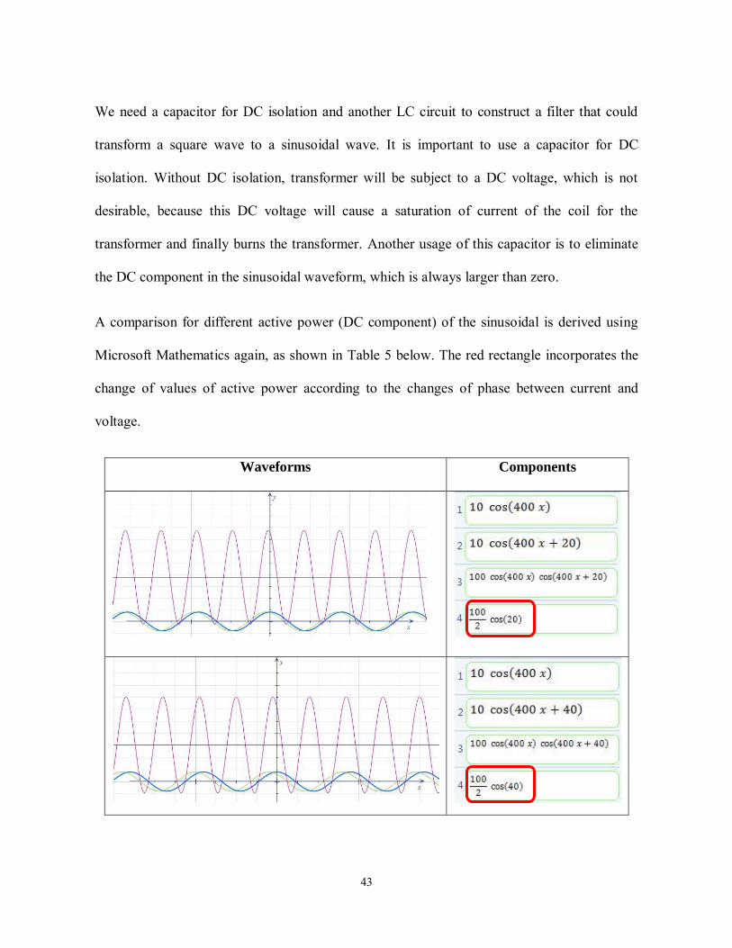
A comparison for different active power (DC component) of the sinusoidal is derived using
Microsoft Mathematics again, as shown in Table 5 below. The red rectangle incorporates the
change of values of active power according to the changes of phase between current and
voltage.
Waveforms Components

44
Table 5: Phase Shift between V and I and Decrease of Active Power (Straight Line)
Above are the explanations of design criteria. Below these criteria must be applied to the real
LED driving circuit. If we assume that the electronic ballast is having current feedback
scheme, which used to stabilize the current flowing through the resonant tank. If this
assumption is made, we could regard the electronic ballast as a current source. Taking away
the fluorescent lamp part, the LED driver and LED lamps could be replaced, as shown in
Figure 18.
Figure 18: Equivalent Circuit of the Ballast and Fluorescent Lamp Model

45
Figure 19: Replacement of LED Driver and LED Unit
Therefore, the final design of the LED driver is shown in Figure 20
Figure 20: Circuit Diagram of LED Driver
The circuit is actually an inverter formed by switches SA and SB through a resonant tank
circuit formed by CA, CB and L. The inverter circuit is actually a ―mirror‖ of the circuit of the
electronic ballast. It actually performs exactly the reversed function of electronic ballast. A
transformer is used to link the electronic ballast and LED driver, as shown by Figure 21.
AC
DC
AC
DC
46
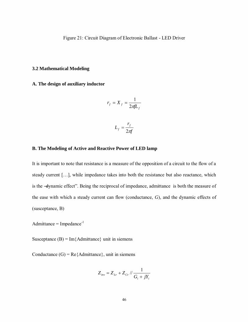
Figure 21: Circuit Diagram of Electronic Ballast - LED Driver
3.2 Mathematical Modeling
A. The design of auxiliary inductor
f
fffL
Xr21
f
rL
f
f2
B. The Modeling of Active and Reactive Power of LED lamp
It is important to note that resistance is a measure of the opposition of a circuit to the flow of a
steady current […], while impedance takes into both the resistance but also reactance, which
is the ―dynamic effect‖. Being the reciprocal of impedance, admittance is both the measure of
the ease with which a steady current can flow (conductance, G), and the dynamic effects of
(susceptance, B)
Admittance = Impedance-1
Susceptance (B) = Im{Admittance} unit in siemens
Conductance (G) = Re{Admittance}, unit in siemens
ii
CrLrinvjYG
ZZZ
1//

47
22 )()(
)(1
)(
)(1
1//1
rii
riir
iir
r
iir
iir
iirr
iir
rinv
CYG
CYjGLj
GYCjLj
jYGCj
jYGCj
jYGCjLj
jYGCjLjZ
22 )(}Re{
rii
iinv
CYG
GZ
, 22 )(
}Im{rii
ririnv
CYG
CYLZ
The active power (real power) PLED and the reactive power QLED of the LED lamp are:
ilampLED GvP2
ilampLED YvQ2
)()(
)()(()(
22
222222
2
2
rilamprilamp
ilampriilampilampinv
lamp
LEDinv
CYVCYV
GVCYGVGViv
Pi
]-[
2
22
rlamp
lamp
LEDinvlampLED CV
v
PivQ ilamp Yv
2
A
ACj
Z
1 ,
B
BCj
Z
1 ,
LjZC

48
Using node analysis of the circuit,
oLC vVVB
-
oC
B
C
A
Clamp
C vZZ
V
Z
VvV BB
B
'-
So oC
B
C
A
CCClamp
C vZZ
V
Z
ZVZvV BB
B
'-
'lamp
A
CoC
B
C
A
CC
C vZ
ZvZ
Z
V
Z
VZV BB
B
Therefore,
'lamp
A
CoC
B
C
A
CC
C vZ
ZvZ
Z
V
Z
VZV BB
B
'lamp
CBCABA
BCo
CBCABA
BAC v
ZZZZZZ
ZZv
ZZZZZZ
ZZV
B
, where vlamp’ is the voltage
across the secondary winding of the transformer, and vo is the inverter voltage on the AC side.
The lamp current ilamp’ is shown as:
A
lamp
CBCABA
CABAo
CBCABA
BA
A
Clamp
lampZ
vZZZZZZ
ZZZZv
ZZZZZZ
ZZ
Z
Vvi B
''
'
It can be seen that the value of ilamp’ is controlled by vlamp’ and v0, which means that the phase
of ilamp’ can be controlled by v0.

49
The active power PLED and reactive power QLED of the LED lamp could be obtained from:
}''Re{ *)()( rmslamprmslampLED ivP
}''Im{ *)()( rmslamprmslampLED ivQ
sincos 0000 vjvevv i
ABA
lamp
LEDCCCLn
vvP
)](1[sin
20
ABA
lampB
ABA
lamp
LEDCCCLn
vLC
CCCLn
vvQ
)](1[
)1(
)](1[
cos22
22
2
0
Here, n is the ratio of transformer, CA, CB and L are components of the resonant tank to be
modeled in the section below.
D. The Modeling of Resonant Tank
Figure 22: Thevenin Circuit Equivalent of Ballast-Driver
50
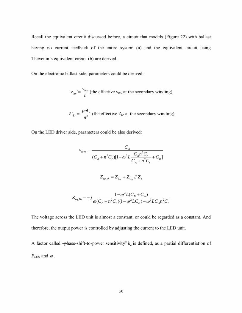
Recall the equivalent circuit discussed before, a circuit that models (Figure 22) with ballast
having no current feedback of the entire system (a) and the equivalent circuit using
Thevenin’s equivalent circuit (b) are derived.
On the electronic ballast side, parameters could be derived:
n
vv inv
inv ' (the effective vinv at the secondary winding)
2'n
LjZ r
Lr
(the effective ZLr at the secondary winding)
On the LED driver side, parameters could be also derived:
]1)[( 2
222
,0
B
rA
rArA
ATh
CCnC
CnCLCnC
Cv
LCCTheq ZZZZBA
//,
rABrA
ABTheq
CnLCLCCnC
CCLjZ 2322
2
, )1)(()(1
The voltage across the LED unit is almost a constant, or could be regarded as a constant. And
therefore, the output power is controlled by adjusting the current to the LED unit.
A factor called ―phase-shift-to-power sensitivity‖ k is defined, as a partial differentiation of
PLED and .

51
ABA
lampLED
CCCLn
vvPk
)](1[
cos2
0
Therefore, by using this factor:
sin)](1[1
02
vv
nP
CCCLlamp
LED
ABA
2
2
0
2
2 )](1[
cos
)](1[)1(
lamp
LED
ABA
lamp
ABA
B
v
nQCCCL
vvn
CCCL
LC
By solving the equations above, the values of CA, CB and L could be calculated:
)cos
1(
)](1[1
0
2
lamp
ABAA
v
vn
CCCLC
A
lamp
B Cvn
vnvC
0
0-cos
ABlamp
AB
A
ABA
B
A
ABA
B
lamp
CLCv
CLCvn
CCCCL
LC
CCCCL
LC
v
vn
L)1(cos)1(
)](1[)1(
))](1[)1((
cos22
20
2
22
2
20
There are three unknowns and three equations. All other parameters in the equations are
already known from the circuit (n, v0, vlamp and ω). Therefore, equations could be solved and
the resonant tank could be designed.

52
The representations of the three values CA, CB and L all involve with cosφ, which means that
the value should actually change with the change of the phase difference. However, this is
impossible in the real case. The three values should be designed with the maximum allowable
phase. This is one of the origins of the inaccuracy of dimming control of the circuit.
3.3 Limitation Analysis
As mentioned in the last section, since the value of the components in the resonant tank is
fixed, the performance of the dimming control function is not accurate enough.
Even though theoretically the dimming range should be from 0% - 100%m, as proved in the
representation of PLED, in practice, it is observed that the dimming range is only between 60%
- 100%. In other words, there is a limitation of this dimmable LED driver proposed in this
research. In fact, the adjustment of phase shift must be only achieved at the range of the rated
power of electronic ballast. Phase adjustment out of this range could not guarantee a proper
work of the electronic ballast. The fact that dimming range does not strictly follow the
mathematical representation is due to this reason.
3.4 Summary of Chapter
In this chapter, circuit modeling and resonant tank modeling were made, in order to realize the
requirement of the LED lamp. Mathematical modeling congested this chapter, and the

53
equations of the power of the LED lamp by adjusting the phase of the switching MOSFETs
were developed. With these derivations, the circuit could be designed.
Phase adjustment is achieved using a MCU in the circuit, it detects the voltage and use A/D
converter to sample it, and then feed it to the MCU. Then the MCU processed it, using
another external voltage, which is obtained using the voltage divider circuit with a variable
resistor. The source code is shown in the appendix section.

54
Chapter 4 Simulation Results
4.1 Introduction
In this section, computer simulations will used to verify all the findings and conclusions for
previous sections. Software was chosen as PSim, because of the flexibility and simplicity of
usage. The sequence of this simulation starts from electronic ballast and the study of PFC
circuit with its implementation on electronic ballast. Then the LED driver circuit is added to
the analysis. Finally, a complete version of PFC circuit, electronic ballast and LED driver is
simulated. This is a thorough simulation of the performance in real applications.
4.2 Simulation of Electronic Ballast
Figure 23: Circuit of Buck-Converter Electronic Ballast
Figure 23 is a simulation of buck-converter resembled, frequency upgrading AC-to-AC
converter, which could be used as an electronic ballast. Please note that this is a buck-

55
converter (DC) manipulation of the high-frequency square wave, therefore, a capacitor
achieving DC isolation C2 needs to be added.
Figure 24: Circuit of Half-Bridge Inverter Electronic Ballast
Figure 24 is a representation of a half-bridge AC-to-AC converter, which is a typical design
for electronic ballast in real applications. Please note that the capacitor C2, achieving DC
isolation is eliminated from this circuit, due to the AC output of half-bridge. The differences
between these two typical designs of electronic ballast have been explained in Chapter 1.
Below is the analysis of the waveforms.
Using equation derived before:
inv
r
rFlinv
r
r
Fl
inv
rFlrrFl
Fl
r VL
CjrV
C
Lj
rV
LjrCLr
rV
Fl
2
56
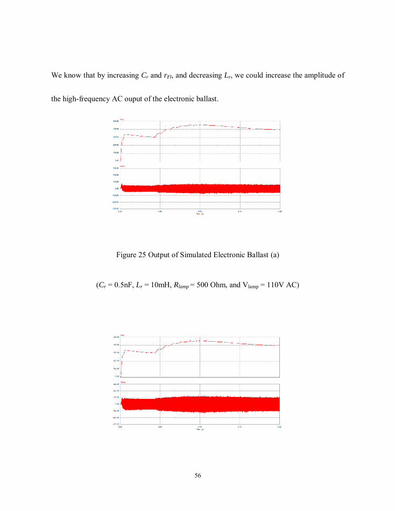
We know that by increasing Cr and rFl, and decreasing Lr, we could increase the amplitude of
the high-frequency AC ouput of the electronic ballast.
Figure 25 Output of Simulated Electronic Ballast (a)
(Cr = 0.5nF, Lr = 10mH, Rlamp = 500 Ohm, and Vlamp = 110V AC)

57
Figure 26 Output of Simulated Electronic Ballast (b)
(Cr = 1nF, Lr = 5mH, Rlamp = 500 Ohm, and Vlamp = 170V AC)
Figure 27 Output of Simulated Electronic Ballast (c)
(Cr = 2nF, Lr = 2mH, Rlamp = 500 Ohm, and Vlamp = 205V AC)
It could be seen that the simulation results matches the calculation above. When Cr is
increasing and Lr is decreasing, the high frequency AC output for the fluorescent lamp is
increasing. However, it is noticed that there are lots of pulsating current components exists in
the input side of the electronic ballast, as shown in Figure 28 and 29.
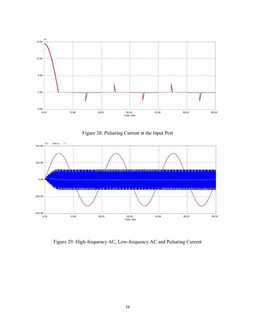
58
Figure 28: Pulsating Current at the Input Port
Figure 29: High-frequency AC, Low-frequency AC and Pulsating Curernt
59
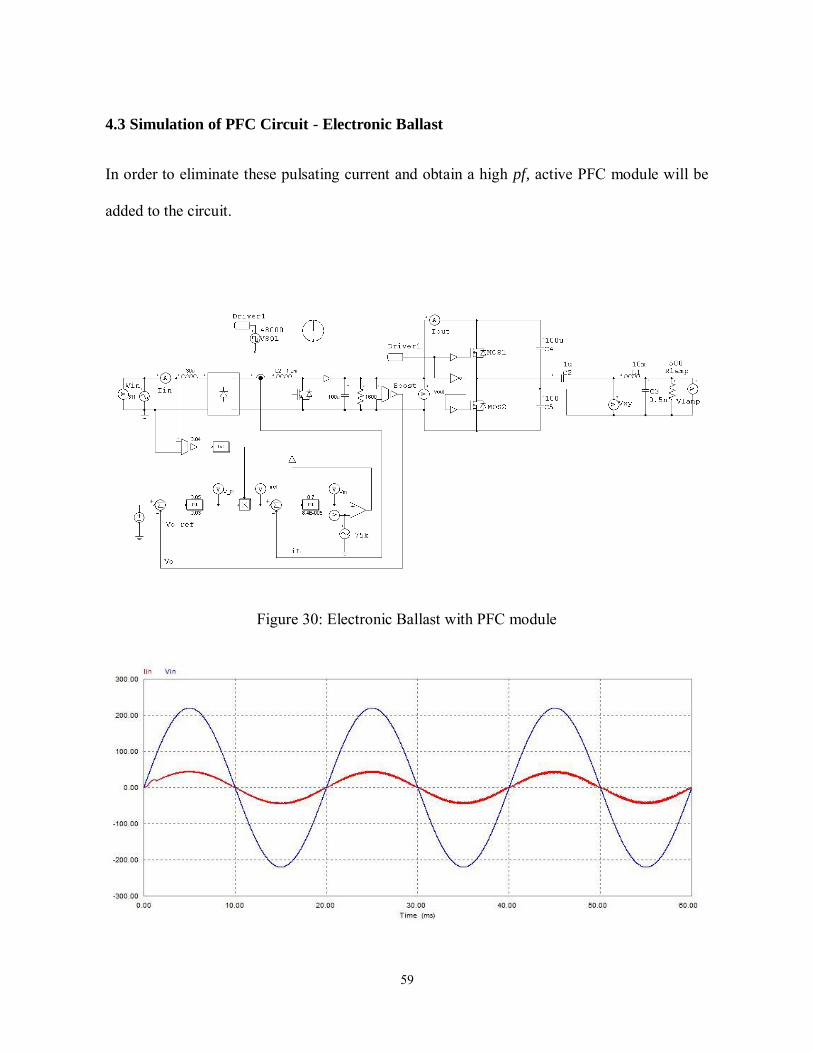
4.3 Simulation of PFC Circuit - Electronic Ballast
In order to eliminate these pulsating current and obtain a high pf, active PFC module will be
added to the circuit.
Figure 30: Electronic Ballast with PFC module

60
Figure 31: Waveform of Vin and Iin, in phase, high pf
4.4 Simulation of Electronic Ballast - LED Driver
In simulation software, a phase adjustment tool must be added to control the gate signal of the
two MOSFETs. A RC filter is used to create a phase shift and assign this phase shift to the
gate signal. Below is an explanation of how the phase shift is determined by using PSim
simulation.
If the voltage is:
)sin(0 tV
The RC circuit is regarded as a voltage divider, so the voltage at the comparator is:
)sin(1
1
0 tV
CjR
CjVcontrol
Using polar form, this voltage can be represented as:
222
0
1 RC
VVcontrol , where )arctan( RC
Therefore, by varying the value of R and C, with a fixed frequency, Vcontrol could be
synchronized with V0 with a controllable phase difference. If Vcontrol could be used to generate
a gate signal to switch the MOSFET of the LED driver, the switching signal could be used to
adjust the waveform of V0, and thus the active power drawn from the electronic ballast.
61
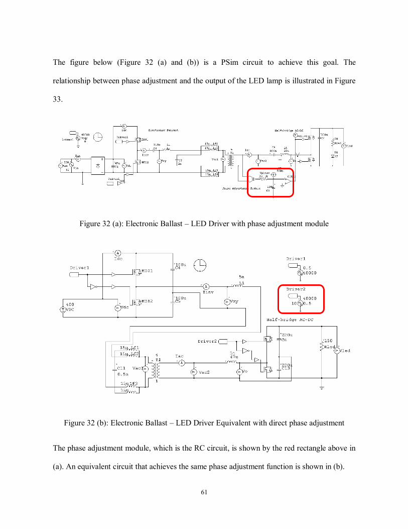
The figure below (Figure 32 (a) and (b)) is a PSim circuit to achieve this goal. The
relationship between phase adjustment and the output of the LED lamp is illustrated in Figure
33.
Figure 32 (a): Electronic Ballast – LED Driver with phase adjustment module
Figure 32 (b): Electronic Ballast – LED Driver Equivalent with direct phase adjustment
The phase adjustment module, which is the RC circuit, is shown by the red rectangle above in
(a). An equivalent circuit that achieves the same phase adjustment function is shown in (b).

62
By adjusting the value of C8, with a fixed value of R2, the phase could be adjusted.
Or the phase could be adjusted directly by inputting phase shift to the attribute column of the
PWM signal generator.
Figure 33 (a): Phase shift = 10 degree, Vled = 7.4V
Figure 33 (b): Phase shift = 30 degree, Vled = 17.4V

63
Figure 33 (c): Phase shift = 90 degree, Vled = 27.4V
Figure 33 (d): Phase shift = 130 degree, Vled = 13.9V
Hence the LED lamp voltage, Vled could be shown in Figure 33 (a) (b) (c) (d) and (e). In the
best scenario (c), the output voltage has around 1% ripple and remained steady at around 27 V,
which is the rated voltage of the LED lamp.

64
However, with an unsuitable phase difference, the voltage value of the waveform will be
degraded, as shown in (d), which means that the phase adjustment scheme has a valid range.
Out of this range, the lamp would not work properly.
Figure 33 (e): Phase shift = 180 degree, Vled = 0.64V
4.5 Simulation of PFC Circuit - Electronic Ballast - LED Driver
The final circuit design is illustrated as Figure 34, the PFC circuit is added before the
electronic ballast, which is a half-bridge version. The LED driver with a phase adjustment RC
tank is added on the secondary winding of the transformer.
This PSim file simulates the real circumstance, where a PFC circuit is embedded in the
electronic ballast and a phase control module is embedded on the LED driver. However, this
phase control module must be a MCU implementation.

65
Figure 34: Final Circuit Diagram of the Electronic Ballast – LED Driver
Figure 35: Analysis of Waveforms Vled, Vac1, Vac2, Vout and vo (25 degrees shift)
The boost-typed PFC circuit firstly converts the output of the AC mains to be a DC output at
Vout, then the half bridge typed electronic ballast inverter converts this DC to a high frequency
AC. The transformer windings Vac1 and Vac2 show the waveform of this AC output.

66
Figure 36: Phase Shift Analysis (25 degrees shift from Vac2 and vo)
Figure 37: Phase Shift Analysis (90 degrees shift from Vac2 and vo)

67
Chapter 5 Experimental Results
Figure 38: Laboratory Equipments for Final Year Project
Figure 39: DC Module Used for MCU

68
Figure 40: LED Units Working at Rated Voltage 27V
Figure 41: LED Unit Composed of Small LED Grid (Left)

69
Figure 42: LED Unit Working under Pure Diode Bridge Rectifier
Figure 43: LED Unit Working under MCU Controlled Dimming Control Mode

70
Figure 44: Circuit Diagram of LED Driver

71
Chapter 6 Conclusion and Future Improvement
In this final year project, a design of LED driver used for retrofit LED lamp that can function
with the output of electronic ballasts for fluorescent lamps has been presented. The driver is
useful for the popular LED replacements for fluorescent lamp market. Background knowledge
about Power Electronics and AC Power were discussed. Key tools for circuit design and
analysis were reiterated. The experimental results match the theoretical prediction of the
unique active/reactive power dimming control method. However, there are some limitations
for this method, and the limitations were discussed.
A further design of LED driver that can be connected to the output of lamp ballast (high-
frequency electronic one or low-frequency magnetic one) or AC mains with dimming control
function needs to be studied. The new driver uses nearly the same principles of the driver
studied in this report. It will be a power converter with controllable input impedance for the
ballast or ac mains, and with its output to be controlled for dc-powered LED. The proposed
universal LED driver will be operated as an AC-to-DC resonant converter with controllable
impedance that are both resistive and reactive (i.e. having both real and imaginary part), so
that the active power and reactive power delivered to the LED can be adjusted, which is the
dimming control function.

72
References
[1]. A Driving Technology for Retrofit LED Lamp for Fluorescent Lighting Fixtures With
Electronic Ballasts, Nan Chen, Student Member, IEEE and Henry Shu-Hung Chung, Senior
Member, IEEE
[2]. A Dimming Module for Controlling Power Supplying to a Fluorescent Lamp Ballasted by
a Nondimmable Electronic Ballast, Nan Chen, Student Member, IEEE, and Henry Shu-hung
Chung, Senior Member, IEEE
[3]. Multi-Year Program Plan FY 09 – FY 15, Solid State Lighting Research and
Development, Prepared by Navigant Consulting, Inc., Radcliffe Advisors, Inc. and SSLS Inc.
[4]. A Very Simple Control Strategy for Power Factor Correctors Driving High-Brightness
Light-Emitting Diodes, J. Sebastian, D.G. Lamar etc.
[5]. Power Driver Topologies and Control Schemes for LEDs, Heinz van der Broeckl, Georg
Sauerlander etc.
[6]. AC Power – See: http://en.wikipedia.org/wiki/AC_power
[7]. AC-to-DC Rectifier – See: http://en.wikipedia.org/wiki/Rectifier
[8]. Admittance – See: http://en.wikipedia.org/wiki/Admittance
[9]. J. Robertson and R. Currie, ―LED replacement for fluorescent lighting,‖ US Patent
6,860,628, Mar 1, 2005.
73
[10]. S. Eiich and H. Kenjiro, ―LED Lighting Unit Applied to a Fluorescent Lighting Fixture,‖
US Patent Application 20070223225, Sep 27, 2007.
[11]. J. Timmermans, J. Raymond, and J. Ivey, ―LED lighting device for replacing fluorescent
tubes,‖ US Patent 7,510,299, Mar 31, 2009.
[12]. J. Kit ―Retrofit LED lamp for fluorescent fixtures without ballast,‖ US Patent
7,507,001B2, Mar 24, 2009.
[13]. C. Hulgan, ―LED retrofit method and kit for converting fluorescent luminaries,‖ US
Patent 6,739,734, May 25, 2004.
[14]. C. Wu and C. Tu, ―Retrofitting of fluorescent tubes with light-emitting diode (LED)
modules for various signs and lighting applications,‖
[15]. E. Sorella and J. J. Robertson, ―LED Replacement Light Tube for Fluorescent Light
Fixture,‖ United States Patent Application 20090261706, Oct 22, 2009.
[16]. L. O. Nielson and A. A. Mangiaracina, ―Fluorescent lighting conversion to LED lighting
using a power converter,‖ US Patent Application 20080266849, Oct 30, 2008.
[17]. Design Considerations for Achieving ZVS in a Half Bridge Inverter that Drives a
Piezoelectric Transformer with No Series Inductor, Svetlana Bronstein and Sam Ben-Yaakov

74
Appendix
PCB Routing Bottom Side
PCB Routing Top Side

75
PCB of LED Driver Circuit
Chrystal: 30 KHz Capacitors:
22 pF*2
CA 880 nF
CB 320 nF
C3 100 nF*1
10 uF*2
47 uF
100 nF*2
Resistors:
5.1KΩ *7
10 Ω *5
R7: 3KΩ
R1: 10KΩ
Transformer (8:2:1) primary winding > 30
mH
ICs:
IC1: IR2104
IC2: LM393 (COM)
Q4, Q5: IRF840
Q1, Q2:2N3906
Inductor:
L44 uH
Diodes:
D2: 1N4007
D3: 1N4148
Component List of LED Driver