thin wideband absorber with optimal thickness …lup.lub.lu.se/search/ws/files/6328653/1581319.pdf1...
TRANSCRIPT

LUND UNIVERSITY
PO Box 117221 00 Lund+46 46-222 00 00
Thin wideband absorber with optimal thickness
Kazemzadeh, Alireza
Published: 2010-01-01
Link to publication
Citation for published version (APA):Kazemzadeh, A. (2010). Thin wideband absorber with optimal thickness. (Technical Report LUTEDX/(TEAT-7192)/1-9/(2010); Vol. TEAT-7192). [Publisher information missing].
General rightsCopyright and moral rights for the publications made accessible in the public portal are retained by the authorsand/or other copyright owners and it is a condition of accessing publications that users recognise and abide by thelegal requirements associated with these rights.
• Users may download and print one copy of any publication from the public portal for the purpose of privatestudy or research. • You may not further distribute the material or use it for any profit-making activity or commercial gain • You may freely distribute the URL identifying the publication in the public portalTake down policyIf you believe that this document breaches copyright please contact us providing details, and we will removeaccess to the work immediately and investigate your claim.

Download date: 15. Jul. 2018
Electromagnetic TheoryDepartment of Electrical and Information TechnologyLund UniversitySweden
CODEN:LUTEDX/(TEAT-7192)/1-9/(2010)
Thin Wideband Absorber withOptimal Thickness
Alireza Kazemzadeh
Alireza [email protected]
Department of Electrical and Information TechnologyElectromagnetic TheoryLund UniversityP.O. Box 118SE-221 00 LundSweden
Editor: Gerhard Kristenssonc© Alireza Kazemzadeh, Lund, April 1, 2010
1
Abstract
The known methods for designing nonmagnetic absorbers usually aim for ei-
ther the reduction of total thickness or increase of absorption bandwidth by
sacricing the other parameter. The conventional circuit analog absorbers aim
for large bandwidths whereas the newly proposed meta-material or optimized
geometry designs try to reduce the thickness of the absorber. By the aid of
the capacitive circuit absorber approach, an optimal method for designing thin
absorbers with practical bandwidths is proposed. An absorber is designed for
the whole radar X-band with total thickness about λ/10. It is shown that the
absorber thickness is satisfactorily close to the theoretical limit. The eect
of mutual coupling on the performance of thin absorbers are investigated and
some techniques for reducing the mutual couplings are suggested.
1 Introduction
Two parameters are usually important in the design of an absorber, the absorptionbandwidth and the total thickness of the design. The ideal situation for a designis to achieve the largest bandwidth with the minimum possible thickness. Simul-taneous optimization of the total thickness and the absorption bandwidth is notan easy task and the published designs usually succeed in achieving one goal bysacricing the other. For achieving large bandwidths, conventional design methodssuch as Jaumann [1, 2] and circuit analog absorbers [810] have been introduced.These absorbers are made of resistive layers separated from each other by dielectricspacers that are quarter of a wavelength thick at the mid-frequency. It is knownthat for obtaining large bandwidths a few resistive/dielectric layers are required.Consequently large bandwidths are achieved in cost of considerable thicknesses. Re-cent investigations have concentrated on low prole absorbers that are thinner thana quarter of wavelength. The designs are usually called ultra thin absorbers and usemeta-material ideas or optimized geometries of frequency selective surfaces (FSS)to match the ground plane to free space [3, 4, 6, 7]. Unfortunately these absorbershave very narrow bandwidths which jeopardize their practicality [9, 10].
The capacitive circuit absorber approach is capable of fullling both of the con-tradictory goals [5]. A systematic method for designing wideband thin absorber withoptimal thickness is presented. First, by the aid of the physical bound introducedby Rozanov [11] a meaningful relationship between bandwidth and total thicknessof an absorber is established. It is shown that for a given frequency response, thetotal thickness of a nonmagnetic absorber cannot be less than a theoretical limit.Then a two layer thin absorber is designed for the whole radar X-band frequencyinterval (8-12GHz). It is shown that the total thickness of the absorber is very closeto the minimum possible thickness dictated by the theoretical limit.

2
2 The relation between total thickness and absorp-
tion frequency response
A basic rule of absorber design is that wider bandwidth requires larger thickness,but is there any physical relation between these quantities? Rozanov has shownthat for any metal backed absorber under normal incident illumination, the inniteintegral of natural logarithm of the reection coecient is bounded from aboveunder certain conditions [11]. The conditions are very general and include all linear,passive, time invariant and causal materials. Therefore, all the meta-material oroptimized geometries and FSS based absorbers are included in this general category.The physical bound is expressed by the following relation:
|∫ ∞
0
ln |R(λ)| dλ | ≤ 2π2∑
i
µs,idi (2.1)
In the above equation R is the reection coecient, λ is the wavelength in freespace and di, µs,i are the thickness and the static permeability of the ith layer of themultilayered slab. For a nonmagnetic absorber the above equation can be rearrangedinto the following form:
d ≥|∫∞
0ln |R(λ)| dλ |
2π2(2.2)
The above equation provides a useful relation between the total thickness of a non-magnetic absorber (d) and its frequency response. It states that that for a givenabsorption frequency response, the total thickness of the absorber cannot be lessthan a theoretical limit. By providing an accurate approximation of the desiredfrequency response, Eq. 2.2 can be used to estimate the minimum possible thicknessof the corresponding absorber. This theoretical thickness is then used as a designobjective. Experience has shown that a linear piecewise approximation of the fre-quency response in dB scale is a fair approximation for the frequency response ofa nonmagnetic absorber. It is very similar to the Bode plots used in lter theorywith the dierence that the frequency is not in logarithmic scale. Therefore, thereection coecient can be expressed as a function of frequency as the following:
R(f) =
−R0(
f−f1
f2−f1) f1 ≤ f ≤ f2
−R0 f2 ≤ f ≤ f3
R0(f−f4
f4−f3) f3 ≤ f ≤ f4
0 otherwise
(2.3)
In the above equation, the R0 is the average absorption level in the absorptionband in dB scale (a positive number). The transition intervals are controlled by thef1 and f4 frequencies and should be selected in a way that they result in practicalslopes for the frequency response. By mapping the frequency response of Eq. 2.3into wavelength domain and using Eq. 2.2, the minimum possible thickness of theabsorber can be calculated. In the next section an absorber is designed for theradar X-band (8− 12 GHz). To dene a design objective, the case with f1 = 6 GHz,f2 = 8 GHz, f3 = 12 GHz, f4 = 16 GHz and R0 = 22 dB is considered throughoutthe paper. For the given values the minimum possible thickness is ≈ 2.8 mm.

3
3 Thin Absorber for the Radar X-Band
After dening the design goals and calculating the minimum possible thickness forthe desired frequency response, it is time to propose a design that can fulll them asclose as possible. A two layer (number of periodic layers) capacitive circuit absorber[5] is able to meet the design goals successfully. All the previous publications on ultrathin absorber are single resistive layer designs [3, 4, 6, 7] and it is for the rst timethat a wideband two layer thin absorber is presented. Capacitive circuit absorber[5] is a modication of the circuit analog absorber [9, 10] approach that resultsin many advantages. The basic idea is to replace the band-stop resonating FSSelements of the circuit analog absorbers with low-pass FSS structures. The low-passelements can be synthesized by simple geometries such as square patches [5]. Thelow-pass behavior of the square patch array has the advantage that its frequencyresponse is not aected by harmonic and anti-resonance frequencies over a very largebandwidth, in contrast to the band-stop resonating elements used in circuit analogabsorbers [5, 810]. The fact simplies the modeling and design of the absorbersignicantly. It can be shown that the capacitive circuit absorber method is a moreexible approach that leads into new applications, impossible to be accomplishedby circuit analog absorber method (some examples have been given in [5]). Amongthe new applications one is the wideband thin absorber with optimal thickness. Animportant advantage of the capacitive circuit method is that the distance betweenFSS layers can be much smaller than quarter-wavelength separations common incircuit analog absorbers [810]. When the distance between FSS layers are abouta quarter of a wavelength, the mutual coupling between the periodic arrays is verylow, in particular if they are embedded in dielectric covers [810]. Therefore, theequivalent circuit models of the circuit analog absorbers are very close to the actualfrequency response of the synthesized absorber (cares must be taken into accountabout harmonic and anti-resonance frequencies). The situation is the same (orbetter owing to avoiding resonances) for thick capacitive circuit absorbers. In a thinabsorber the total thickness of the design is in order of λ/10 or less. Consequently,the distance between the FSS layers and the distance between the rst periodic layerand the ground plane are much smaller than quarter of a wavelength. Therefore, itis expected that the mutual coupling between layers can be high and destructive ifthey are not treated properly. There might be a perceptible dierence between thefrequency response of the equivalent circuit model and the actual full-wave responseof the synthesized absorber. These facts and the potential of the capacitive circuitabsorber method to handle the problem is illustrated in the following.
The rst step in the design of the absorber is to nd an equivalent circuit modelthat can match the ground plane to the free space over the desired frequency interval.Then, the circuit model is synthesized by proper FSS elements and dielectric layers.If the separation between the FSS layers are large enough, the frequency responseof the circuit model and the actual absorber are very similar. In our case where thetotal thickness of the absorber is only λ/10, cares must be take into account fromthe beginning in the circuit model. The mutual coupling between the FSS layersand the ground plane must be reduced as much as possible by proper techniques.

4
d1dcd c
C 2 1234C 1
R 1
d2"c "c
Figure 1: The schematic of the equivalent circuit model of the thin widebandabsorber.
εc d1( mm) dc( mm) d2( mm)1 0.8 0.2 1.9
3.8 0.8 0.2 1.9
εc R1( Ω) C1( pF) C2( pF)1 37.3 0.305 0.061
3.8 39.6 0.31 0.06
Table 1: The equivalent circuit model parameters for the thin absorbers accompa-nied with the permittivity of the corresponding dielectric cover used in the designs.Other dielectric layers have permittivity values equal to one.
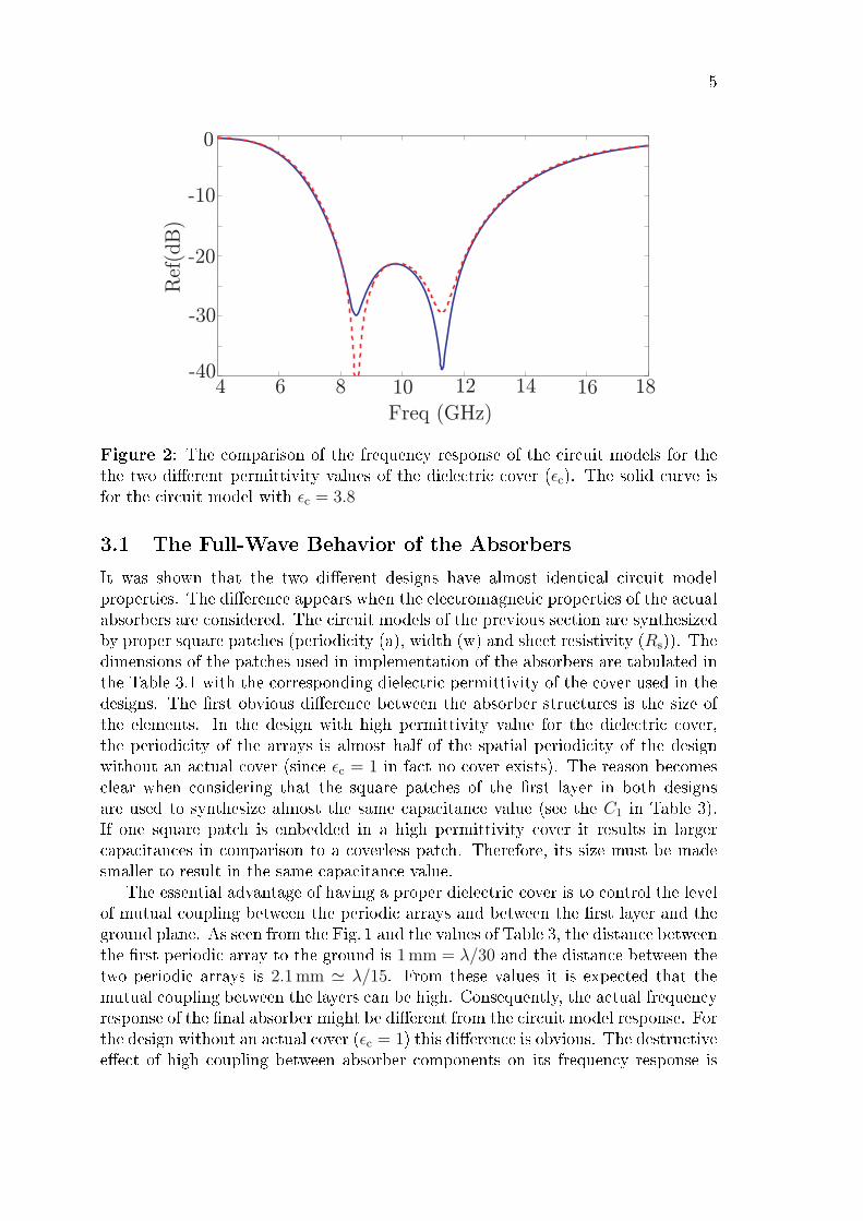
The fact is illustrated by two dierent design examples. Both of the designs are twolayer absorbers with circuit models that diers only in one parameter. It is shownthat this small dierence causes a large eect on the full-wave frequency responseof the absorbers. The equivalent circuit model of the thin absorber is shown inFig. 1. As seen from the equivalent circuit model, only low-pass elements are usedto match the ground-plane to the free space impedance (the port symbol in Fig. 1).The rst series RC circuit (R1 and C1 in Fig. 1) is embedded in a dielectric coverwith permittivity εc and thickness dc. The dielectric cover with proper permittivityresults in signicant advantages, one is the reduction of the mutual coupling eects.The best way to illustrate the mechanism is through examples. Two absorbers withthe same circuit models are designed for the radar X-band with the only dierencethat the permittivity of the dielectric cover is varied between them (εc in Fig. 1). Thevalues of the circuit parameters are tabulated for both designs in Table 3. As seenfrom the values, the two circuit models are very similar except they have dierentpermittivity values for the dielectric cover. The variation of the permittivity of thedielectric cover has a minor eect on the frequency response of the circuit models.The fact can be seen clearly in Fig. 2 where the frequency responses of the two circuitmodels are compared. Both designs have the same total thickness of 3.1 mm whichis practically close to the minimum possible thickness calculated in the previoussection (2.8 mm). Therefore, as far as circuit models are considered the designs arealmost identical.
5
4 6 8 10 12 14 16 18-40
-30
-20
-10
0
Freq (GHz)
Ref
(dB
)
Figure 2: The comparison of the frequency response of the circuit models for thethe two dierent permittivity values of the dielectric cover (εc). The solid curve isfor the circuit model with εc = 3.8
3.1 The Full-Wave Behavior of the Absorbers
It was shown that the two dierent designs have almost identical circuit modelproperties. The dierence appears when the electromagnetic properties of the actualabsorbers are considered. The circuit models of the previous section are synthesizedby proper square patches (periodicity (a), width (w) and sheet resistivity (Rs)). Thedimensions of the patches used in implementation of the absorbers are tabulated inthe Table 3.1 with the corresponding dielectric permittivity of the cover used in thedesigns. The rst obvious dierence between the absorber structures is the size ofthe elements. In the design with high permittivity value for the dielectric cover,the periodicity of the arrays is almost half of the spatial periodicity of the designwithout an actual cover (since εc = 1 in fact no cover exists). The reason becomesclear when considering that the square patches of the rst layer in both designsare used to synthesize almost the same capacitance value (see the C1 in Table 3).If one square patch is embedded in a high permittivity cover it results in largercapacitances in comparison to a coverless patch. Therefore, its size must be madesmaller to result in the same capacitance value.
The essential advantage of having a proper dielectric cover is to control the levelof mutual coupling between the periodic arrays and between the rst layer and theground plane. As seen from the Fig. 1 and the values of Table 3, the distance betweenthe rst periodic array to the ground is 1 mm = λ/30 and the distance between thetwo periodic arrays is 2.1 mm ' λ/15. From these values it is expected that themutual coupling between the layers can be high. Consequently, the actual frequencyresponse of the nal absorber might be dierent from the circuit model response. Forthe design without an actual cover (εc = 1) this dierence is obvious. The destructiveeect of high coupling between absorber components on its frequency response is

6
εc a1( mm) w1( mm) a2( mm) w2( mm)1 12 11.9 6 5.4
3.8 6.8 6.6 3.4 3.3
Table 2: The parameters of the square patches used in the absorbers accompaniedwith the permittivity of the corresponding dielectric cover used in the designs.
4 6 8 10 12 14 16 18-40
-30
-20
-10
0
Freq (GHz)
Ref
(dB
)
Figure 3: Comparison of the frequency response of the actual absorber with theequivalent circuit model used to construct it for the case of low permittivity dielectriccover (εc = 1). The solid curve shows the full wave simulation (CST MicrowaveStudio).
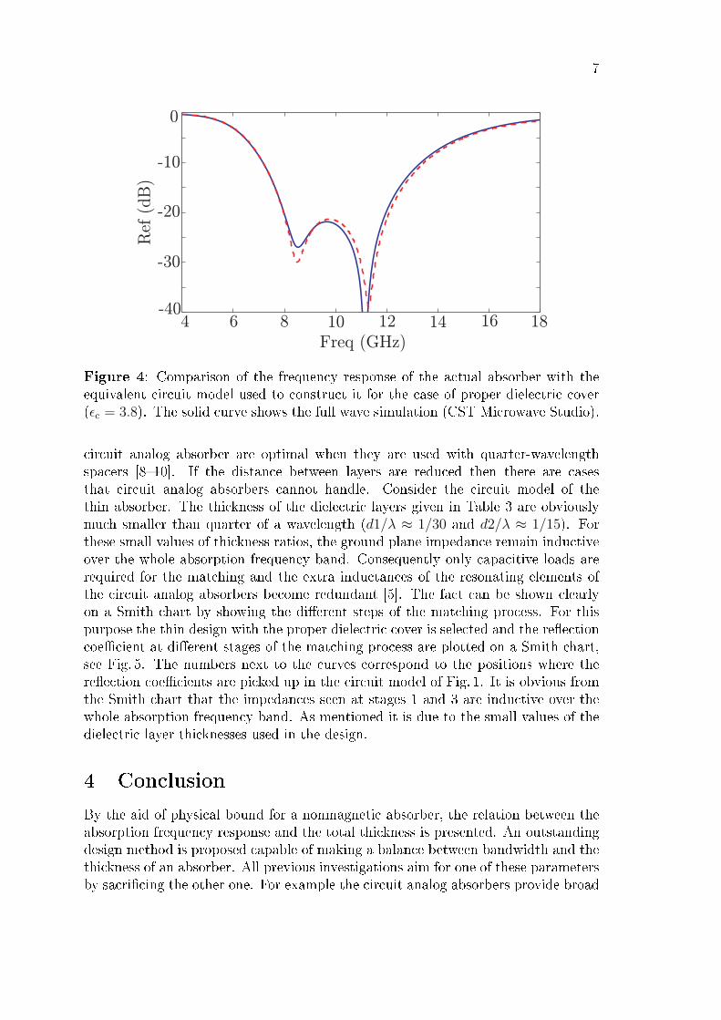
shown in Fig. 3. A proper dielectric cover can concentrate the eld distribution to thevicinity of the periodic array. Therefore, when the rst periodic layer is embeddedin a high permittivity dielectric cover (εc = 3.8), the presence of the ground planeand the next periodic array do not inuence its eld distribution. As a result itsequivalent impedance is not altered by the presence of the ground plane and thesecond periodic array. Moreover, by increasing the width to periodicity ratio of thesecond square patch (w2/a2) from 0.9 in the design with low permittivity cover to0.97 in the design with high permittivity, the eld distribution of the second arrayis more concentrated to the vicinity of the patches. Therefore, the coupling betweenthe two periodic arrays is reduced one more time. All these eects together causethat the frequency response of the nal design to be preserved in the transition fromthe circuit model to the actual absorber. Comparison of the frequency response ofthe circuit model and the full-wave simulation in Fig.4 veries the fact.
3.2 Why Capacitive Circuit Absorber Method
Before ending this section it is important to explain why the circuit analog absorberapproach cannot be used for thin wideband absorbers. The main reason is that
7
4 6 8 10 12 14 16 18-40
-30
-20
-10
0
Freq (GHz)
Ref
(dB
)
Figure 4: Comparison of the frequency response of the actual absorber with theequivalent circuit model used to construct it for the case of proper dielectric cover(εc = 3.8). The solid curve shows the full wave simulation (CST Microwave Studio).
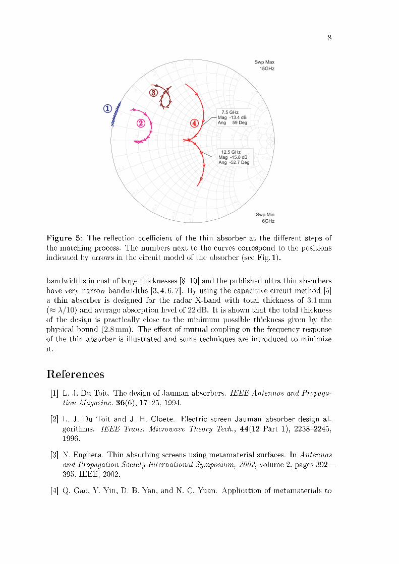
circuit analog absorber are optimal when they are used with quarter-wavelengthspacers [810]. If the distance between layers are reduced then there are casesthat circuit analog absorbers cannot handle. Consider the circuit model of thethin absorber. The thickness of the dielectric layers given in Table 3 are obviouslymuch smaller than quarter of a wavelength (d1/λ ≈ 1/30 and d2/λ ≈ 1/15). Forthese small values of thickness ratios, the ground plane impedance remain inductiveover the whole absorption frequency band. Consequently only capacitive loads arerequired for the matching and the extra inductances of the resonating elements ofthe circuit analog absorbers become redundant [5]. The fact can be shown clearlyon a Smith chart by showing the dierent steps of the matching process. For thispurpose the thin design with the proper dielectric cover is selected and the reectioncoecient at dierent stages of the matching process are plotted on a Smith chart,see Fig. 5. The numbers next to the curves correspond to the positions where thereection coecients are picked up in the circuit model of Fig. 1. It is obvious fromthe Smith chart that the impedances seen at stages 1 and 3 are inductive over thewhole absorption frequency band. As mentioned it is due to the small values of thedielectric layer thicknesses used in the design.
4 Conclusion
By the aid of physical bound for a nonmagnetic absorber, the relation between theabsorption frequency response and the total thickness is presented. An outstandingdesign method is proposed capable of making a balance between bandwidth and thethickness of an absorber. All previous investigations aim for one of these parametersby sacricing the other one. For example the circuit analog absorbers provide broad
8
0 1.0
1.0
-1.0
10.0
10.0
-10.0
5.0
5.0
-5.0
2.0
2.0
-2.0
3.0
3.0
-3.0
4.0
4.0
-4.0
0.2
0.2
-0.2
0.4
0.4
-0.4
0.6
0.6
-0.6
0.8
0.8
-0.8
Swp Max15GHz
Swp Min6GHz
12.5 GHzMag -15.8 dBAng -52.7 Deg
7.5 GHzMag -13.4 dBAng 59 Deg
1
2
3
4
Figure 5: The reection coecient of the thin absorber at the dierent steps ofthe matching process. The numbers next to the curves correspond to the positionsindicated by arrows in the circuit model of the absorber (see Fig. 1).
bandwidths in cost of large thicknesses [810] and the published ultra thin absorbershave very narrow bandwidths [3, 4, 6, 7]. By using the capacitive circuit method [5]a thin absorber is designed for the radar X-band with total thickness of 3.1 mm(≈ λ/10) and average absorption level of 22 dB. It is shown that the total thicknessof the design is practically close to the minimum possible thickness given by thephysical bound (2.8 mm). The eect of mutual coupling on the frequency responseof the thin absorber is illustrated and some techniques are introduced to minimizeit.
References
[1] L. J. Du Toit. The design of Jauman absorbers. IEEE Antennas and Propaga-
tion Magazine, 36(6), 1725, 1994.
[2] L. J. Du Toit and J. H. Cloete. Electric screen Jauman absorber design al-gorithms. IEEE Trans. Microwave Theory Tech., 44(12 Part 1), 22382245,1996.
[3] N. Engheta. Thin absorbing screens using metamaterial surfaces. In Antennas
and Propagation Society International Symposium, 2002, volume 2, pages 392395. IEEE, 2002.
[4] Q. Gao, Y. Yin, D. B. Yan, and N. C. Yuan. Application of metamaterials to

9
ultra-thin radar-absorbing material design. Electronics Letters, 41, 936, 2005.
[5] A. Kazem Zadeh and A. Karlsson. Capacitive circuit method for fast andecient design of wideband radar absorbers. IEEE Trans. Antennas Propagat.,57(8), 23072314, August 2009.
[6] D. J. Kern and D. H. Werner. A genetic algorithm approach to the design ofultra-thin electromagnetic bandgap absorbers. Microwave Opt. Techn. Lett.,38(1), 6164, 2003.
[7] H. Mosallaei and K. Sarabandi. A one-layer ultra-thin meta-surface absorber.In Antennas and Propagation Society International Symposium, 2005 IEEE,volume 1, pages 615618. IEEE, 2005.
[8] B. Munk. Frequency Selective Surfaces: Theory and Design. John Wiley &Sons, New York, 2000.
[9] B. Munk. Metamaterials: Critique and Alternatives. John Wiley & Sons, NewYork, 2009.
[10] B. A. Munk, P. Munk, and J. Pryor. On designing Jaumann and circuit analogabsorbers (CA absorbers) for oblique angle of incidence. IEEE Trans. Antennas
Propagat., 55(1), 186193, January 2007.
[11] K. N. Rozanov. Ultimate thickness to bandwidth ratio of radar absorbers.IEEE Trans. Antennas Propagat., 48(8), 12301234, August 2000.