thin solid films - university of minnesota · 2 (99.99% purity) ceramic target in a aja-atc-2000...
TRANSCRIPT

Thin Solid Films 520 (2012) 2554–2561
Contents lists available at SciVerse ScienceDirect
Thin Solid Films
j ourna l homepage: www.e lsev ie r .com/ locate / ts f
Sputter deposition of semicrystalline tin dioxide films
B. Selin Tosun a, Rebekah K. Feist b, Aloysius Gunawan a, K. Andre Mkhoyan a,Stephen A. Campbell c, Eray S. Aydil a,⁎a Department of Chemical Engineering and Materials Science, University of Minnesota, 421 Washington Avenue SE, Minneapolis, MN 55455, USAb Dow Solar Solutions, The Dow Chemical Company, 1381 Building, Office 201, Midland, MI 48667, USAc Department of Electrical and Computer Engineering, 200 Union Street SE, Minneapolis, MN 55455, USA
⁎ Corresponding author. Tel.: +1 612 625 8593; fax:E-mail address: [email protected] (E.S. Aydil).
0040-6090/$ – see front matter © 2011 Elsevier B.V. Alldoi:10.1016/j.tsf.2011.10.169
a b s t r a c t
a r t i c l e i n f oArticle history:Received 10 June 2011Received in revised form 29 October 2011Accepted 31 October 2011Available online 6 November 2011
Keywords:Tin dioxideSemicrystallineSputteringAmorphousX-ray diffractionElectrical properties
Tin dioxide is emerging as an important material for use in copper indium gallium diselenide based solarcells. Amorphous tin dioxide may be used as a glass overlayer for covering the entire device and protectingit against water permeation. Tin dioxide is also a viable semiconductor candidate to replace the wide bandgap zinc oxide window layer to improve the long-term device reliability. The film properties required bythese two applications are different. Amorphous films have superior water permeation resistance while poly-crystalline films generally have better charge carrier transport properties. Thus, it is important to understandhow to tune the structure of tin dioxide films between amorphous and polycrystalline. Using X-ray diffrac-tion (XRD) and Hall-effect measurements, we have studied the structure and electrical properties of tin diox-ide films deposited by magnetron sputtering as a function of deposition temperature, sputtering power, feedgas composition and film thickness. Films deposited at room temperature are semicrystalline with nanome-ter size SnO2 crystals embedded in an amorphous matrix. Film crystallinity increases with deposition temper-ature. When the films are crystalline, the X-ray diffraction intensity pattern is different than that of thepowder diffraction pattern indicating that the films are textured with (101) and (211) directions orientedparallel to the surface normal. This texturing is observed on a variety of substrates including soda–limeglass (SLG), Mo-coated soda–lime glass and (100) silicon. Addition of oxygen to the sputtering gas, argon, in-creases the crystallinity and changes the orientation of the tin dioxide grains: (110) XRD intensity increasesrelative to the (101) and (211) diffraction peaks and this effect is observed both on Mo-coated SLG and (100)silicon wafers. Films with resistivities ranging between 8 mΩ cm and 800 mΩ cm could be deposited. Thefilms are n-type with carrier concentrations in the 3×1018 cm−3 to 3×1020 cm−3 range. Carrier concentra-tion decreases when the oxygen concentration in the feed gas is above 5%. Electron mobilities range from 1 to7 cm2/V s and increase with increasing film thickness, oxygen addition to the feed gas and film crystallinity.Electron mobilities in the 1–3 cm2/V s range can be obtained even in semicrystalline films. Initial depositionrates range from 4 nm/min at low sputtering power to 11 nm/min at higher powers. However, depositionrate decreases with deposition time by as much as 30%.
© 2011 Elsevier B.V. All rights reserved.
1. Introduction
Thin tin dioxide (SnO2) films find applications in a wide variety ofdevices such as sensors and solar cells [1–4]. SnO2 is a wide band gap(3.8 eV) semiconductor that crystallizes in tetragonal Cassiterritecrystal structure with lattice parameters a=b=4.737 Å andc=3.185 Å. Although, SnO2 thin films have been used in gas sensorsand as transparent conducting electrodes, its high chemical stabilityalso makes it an attractive replacement for wide band gap semicon-ductor oxides such as ZnO. Tin dioxide has been deposited on varioussubstrates including Si [1,5], glass slides [2,5–9], quartz [10], InSb [3]
+1 612 626 7246.
rights reserved.
and InP [4]. Many techniques such as sol–gel deposition [11], chemi-cal bath deposition from SnCl4[12], chemical vapor deposition [13],spray pyrolysis [14], electron beam evaporation [9,15], thermal evap-oration [16] and sputtering [1–8,10,17–19] have been used to depositSnO2 films. In most studies where intrinsic SnO2 was studied, thefilms have been deposited by reactive sputtering of metallic tin (Sn)target under O2/Ar atmosphere [1,3–4]. Films deposited at low O2
concentration in the feed gas show metallic characteristics [1]. Inhigh power DC sputtering, the films consist mostly of the mono-oxide phase [1,6,8]. Most of the research on sputtered SnO2 films fo-cused on depositing n-type films with high conductivity by dopingwith Sb [6–8,10,18–19]. SnO2:Sb has been studied both with reactivesputtering of Sn:Sb (95.5% weight purity) metallic targets using Ar/O2
gas [6,8] and with RF sputtering of SnO2 ceramic targets with Ar gas[7,10,18–19]. Increase in deposition rates, grain sizes, carrier
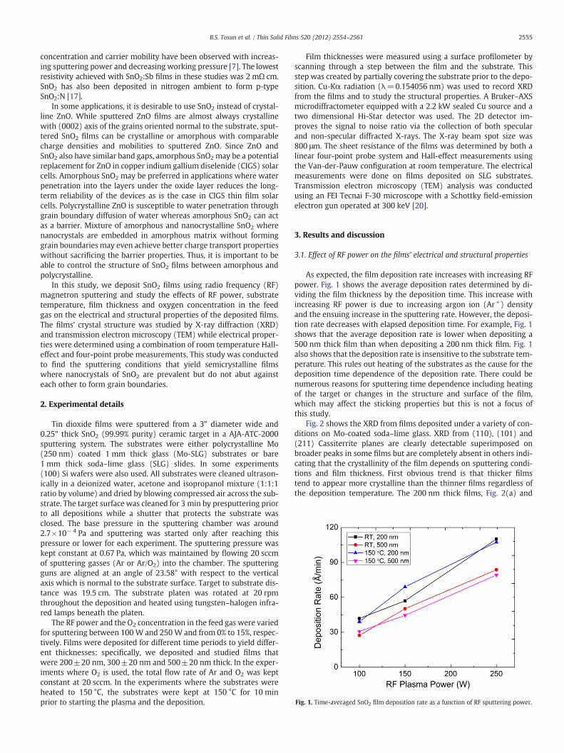
Fig. 1. Time-averaged SnO2 film deposition rate as a function of RF sputtering power.
2555B.S. Tosun et al. / Thin Solid Films 520 (2012) 2554–2561
concentration and carrier mobility have been observed with increas-ing sputtering power and decreasing working pressure [7]. The lowestresistivity achieved with SnO2:Sb films in these studies was 2 mΩ cm.SnO2 has also been deposited in nitrogen ambient to form p-typeSnO2:N [17].
In some applications, it is desirable to use SnO2 instead of crystal-line ZnO. While sputtered ZnO films are almost always crystallinewith (0002) axis of the grains oriented normal to the substrate, sput-tered SnO2 films can be crystalline or amorphous with comparablecharge densities and mobilities to sputtered ZnO. Since ZnO andSnO2 also have similar band gaps, amorphous SnO2 may be a potentialreplacement for ZnO in copper indium gallium diselenide (CIGS) solarcells. Amorphous SnO2 may be preferred in applications where waterpenetration into the layers under the oxide layer reduces the long-term reliability of the devices as is the case in CIGS thin film solarcells. Polycrystalline ZnO is susceptible to water penetration throughgrain boundary diffusion of water whereas amorphous SnO2 can actas a barrier. Mixture of amorphous and nanocrystalline SnO2 wherenanocrystals are embedded in amorphous matrix without forminggrain boundaries may even achieve better charge transport propertieswithout sacrificing the barrier properties. Thus, it is important to beable to control the structure of SnO2 films between amorphous andpolycrystalline.
In this study, we deposit SnO2 films using radio frequency (RF)magnetron sputtering and study the effects of RF power, substratetemperature, film thickness and oxygen concentration in the feedgas on the electrical and structural properties of the deposited films.The films' crystal structure was studied by X-ray diffraction (XRD)and transmission electron microscopy (TEM) while electrical proper-ties were determined using a combination of room temperature Hall-effect and four-point probe measurements. This study was conductedto find the sputtering conditions that yield semicrystalline filmswhere nanocrystals of SnO2 are prevalent but do not abut againsteach other to form grain boundaries.
2. Experimental details
Tin dioxide films were sputtered from a 3" diameter wide and0.25" thick SnO2 (99.99% purity) ceramic target in a AJA-ATC-2000sputtering system. The substrates were either polycrystalline Mo(250 nm) coated 1 mm thick glass (Mo-SLG) substrates or bare1 mm thick soda–lime glass (SLG) slides. In some experiments(100) Si wafers were also used. All substrates were cleaned ultrason-ically in a deionized water, acetone and isopropanol mixture (1:1:1ratio by volume) and dried by blowing compressed air across the sub-strate. The target surface was cleaned for 3 min by presputtering priorto all depositions while a shutter that protects the substrate wasclosed. The base pressure in the sputtering chamber was around2.7×10−4 Pa and sputtering was started only after reaching thispressure or lower for each experiment. The sputtering pressure waskept constant at 0.67 Pa, which was maintained by flowing 20 sccmof sputtering gasses (Ar or Ar/O2) into the chamber. The sputteringguns are aligned at an angle of 23.58° with respect to the verticalaxis which is normal to the substrate surface. Target to substrate dis-tance was 19.5 cm. The substrate platen was rotated at 20 rpmthroughout the deposition and heated using tungsten–halogen infra-red lamps beneath the platen.
The RF power and the O2 concentration in the feed gas were variedfor sputtering between 100 W and 250 W and from 0% to 15%, respec-tively. Films were deposited for different time periods to yield differ-ent thicknesses: specifically, we deposited and studied films thatwere 200±20 nm, 300±20 nm and 500±20 nm thick. In the exper-iments where O2 is used, the total flow rate of Ar and O2 was keptconstant at 20 sccm. In the experiments where the substrates wereheated to 150 °C, the substrates were kept at 150 °C for 10 minprior to starting the plasma and the deposition.
Film thicknesses were measured using a surface profilometer byscanning through a step between the film and the substrate. Thisstep was created by partially covering the substrate prior to the depo-sition. Cu-Kα radiation (λ=0.154056 nm) was used to record XRDfrom the films and to study the structural properties. A Bruker–AXSmicrodiffractometer equipped with a 2.2 kW sealed Cu source and atwo dimensional Hi-Star detector was used. The 2D detector im-proves the signal to noise ratio via the collection of both specularand non-specular diffracted X-rays. The X-ray beam spot size was800 μm. The sheet resistance of the films was determined by both alinear four-point probe system and Hall-effect measurements usingthe Van-der-Pauw configuration at room temperature. The electricalmeasurements were done on films deposited on SLG substrates.Transmission electron microscopy (TEM) analysis was conductedusing an FEI Tecnai F-30 microscope with a Schottky field-emissionelectron gun operated at 300 keV [20].
3. Results and discussion
3.1. Effect of RF power on the films' electrical and structural properties
As expected, the film deposition rate increases with increasing RFpower. Fig. 1 shows the average deposition rates determined by di-viding the film thickness by the deposition time. This increase withincreasing RF power is due to increasing argon ion (Ar+) densityand the ensuing increase in the sputtering rate. However, the deposi-tion rate decreases with elapsed deposition time. For example, Fig. 1shows that the average deposition rate is lower when depositing a500 nm thick film than when depositing a 200 nm thick film. Fig. 1also shows that the deposition rate is insensitive to the substrate tem-perature. This rules out heating of the substrates as the cause for thedeposition time dependence of the deposition rate. There could benumerous reasons for sputtering time dependence including heatingof the target or changes in the structure and surface of the film,which may affect the sticking properties but this is not a focus ofthis study.
Fig. 2 shows the XRD from films deposited under a variety of con-ditions on Mo-coated soda–lime glass. XRD from (110), (101) and(211) Cassiterrite planes are clearly detectable superimposed onbroader peaks in some films but are completely absent in others indi-cating that the crystallinity of the film depends on sputtering condi-tions and film thickness. First obvious trend is that thicker filmstend to appear more crystalline than the thinner films regardless ofthe deposition temperature. The 200 nm thick films, Fig. 2(a) and

Fig. 2. X-ray diffraction pattern from SnO2 films deposited using different RF sputtering powers. XRD from 200 nm thick SnO2 films deposited (a) at room temperature and (b) at150 °C. XRD from 500 nm thick SnO2 films deposited (c) at room temperature and (d) at 150 °C. The SnO2 diffractions are labeled with Miller indices whereas the Mo (110) peak at40.5° is labeled as Mo.
2556 B.S. Tosun et al. / Thin Solid Films 520 (2012) 2554–2561
(b), show amorphous diffraction pattern with very weak (101) and(211) peaks, while the 500 nm films show distinct (101) and (211)peaks, Fig. 2(c) and (d). Second, increasing the substrate temperaturefrom room temperature to 150 °C also increases crystallinity. InFig. 2(d), which shows the XRD from a 500 nm thick film depositedat 150 °C, the (110), (101) and (210) peak intensities are all muchmore intense than those in Fig. 2(c), the XRD for a 500 nm thickfilm deposited at room temperature. Third, increasing the RF plasmapower also appears to increase the crystallinity, though this effect ismuch less obvious than the changes due to film thickness and sub-strate temperature.
Fig. 3 shows the scanning electron micrograph (SEM) of the500 nm thick SnO2 film deposited using 250 W RF power at 150 °C.The film was grown on (100) Si substrates. The columnar grains of
Fig. 3. Scanning electron micrograph of SnO2 films deposited on Si (100) substrates at250 W RF power and at 150 °C.
the film are aligned along the (101) plane normal to the (100) Si sur-face. As it is clear from the SEM micrograph, the deposited film issmooth and continuous over the substrate. Other films also showedsimilar characteristics.
The broad diffraction spanning the range 20° to 37° is present onfilms deposited on all the substrates (SLG, Mo-SLG and (100) Si)and increases with increasing SnO2 thickness suggesting that it isdue to SnO2. Such broad diffraction can originate from amorphousglasses. We attribute absence of sharper diffractions but presence ofthis broad peak to the presence of amorphous SnO2 in the film.Thus, we conclude that thin (200 nm or less) films deposited at lowRF powers and low temperatures tend to contain amorphous SnO2
but the film crystallinity increases with increasing film thickness, sub-strate temperature and RF power. Whether crystalline regions exist infilms deposited at room temperature and in 200 nm thin films cannotbe concluded from XRD alone. The diffraction peak from the nano-crystals overlaps with the broad amorphous feature. To address thisissue we examined the films using cross sectional TEM. We foundthat the 200 nm thick films deposited at room temperature consistedof 5–10 nm SnO2 nanocrystals embedded in an amorphous SnO2 ma-trix. The nanocrystals are surrounded by amorphous SnO2 and do notabut against each other. Thus, despite its nanocrystalline structure thefilms do not contain any grain boundaries. Fig. 4(a) and (b) showshigh-resolution TEM images of the SnO2 films grown using 250 WRF at room temperature and 250 W RF at 150 °C. These films were de-posited on native oxide covered Si substrates to facilitate TEM whileapproximating deposition on glass substrates. The selected area elec-tron diffraction (SAED) patterns obtained from the films confirm thepresence of both amorphous and crystalline components in bothfilms. The film grown using 250 W RF at 150 °C exhibits more intensepolycrystalline-like diffraction ring indicative of higher crystallinecontent than that of 250 W RF at room temperature.
The grain sizes, determined from the full width at half maximumof the XRD peaks using Scherer analysis are shown in Fig. 5 as a
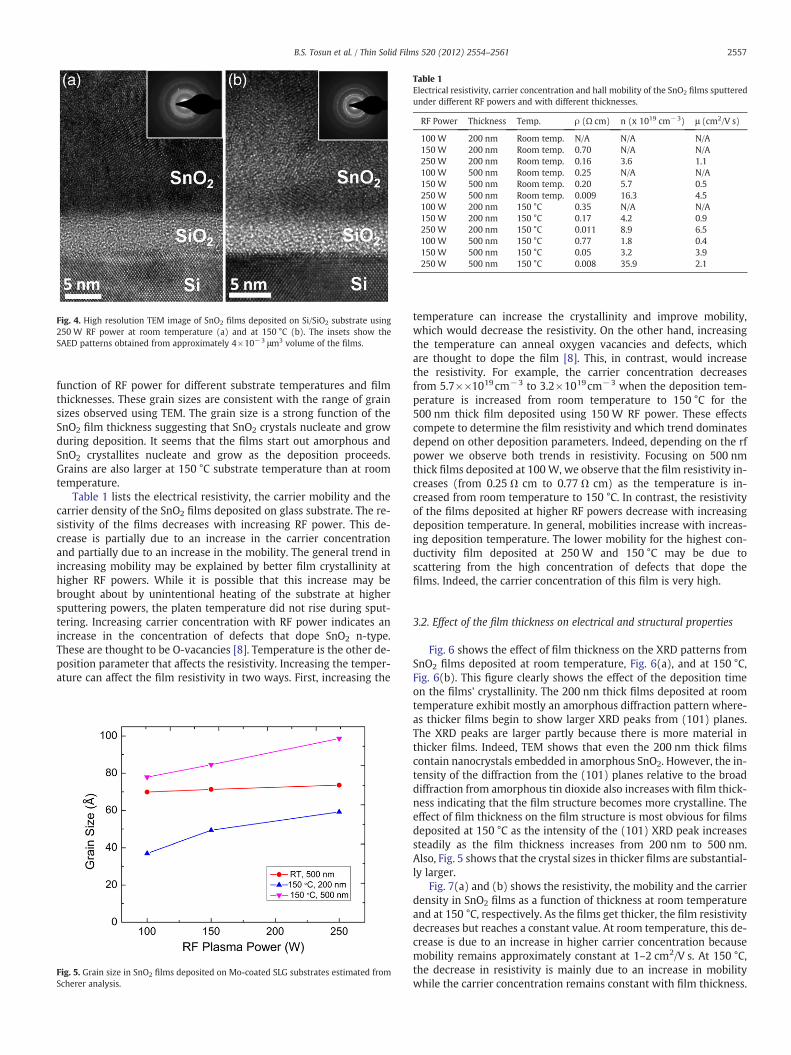
Fig. 4. High resolution TEM image of SnO2 films deposited on Si/SiO2 substrate using250 W RF power at room temperature (a) and at 150 °C (b). The insets show theSAED patterns obtained from approximately 4×10⁻³ μm3 volume of the films.
Table 1Electrical resistivity, carrier concentration and hall mobility of the SnO2 films sputteredunder different RF powers and with different thicknesses.
RF Power Thickness Temp. ρ (Ω cm) n (x 1019 cm−3) μ (cm2/V s)
100 W 200 nm Room temp. N/A N/A N/A150 W 200 nm Room temp. 0.70 N/A N/A250 W 200 nm Room temp. 0.16 3.6 1.1100 W 500 nm Room temp. 0.25 N/A N/A150 W 500 nm Room temp. 0.20 5.7 0.5250 W 500 nm Room temp. 0.009 16.3 4.5100 W 200 nm 150 °C 0.35 N/A N/A150 W 200 nm 150 °C 0.17 4.2 0.9250 W 200 nm 150 °C 0.011 8.9 6.5100 W 500 nm 150 °C 0.77 1.8 0.4150 W 500 nm 150 °C 0.05 3.2 3.9250 W 500 nm 150 °C 0.008 35.9 2.1
2557B.S. Tosun et al. / Thin Solid Films 520 (2012) 2554–2561
function of RF power for different substrate temperatures and filmthicknesses. These grain sizes are consistent with the range of grainsizes observed using TEM. The grain size is a strong function of theSnO2 film thickness suggesting that SnO2 crystals nucleate and growduring deposition. It seems that the films start out amorphous andSnO2 crystallites nucleate and grow as the deposition proceeds.Grains are also larger at 150 °C substrate temperature than at roomtemperature.
Table 1 lists the electrical resistivity, the carrier mobility and thecarrier density of the SnO2 films deposited on glass substrate. The re-sistivity of the films decreases with increasing RF power. This de-crease is partially due to an increase in the carrier concentrationand partially due to an increase in the mobility. The general trend inincreasing mobility may be explained by better film crystallinity athigher RF powers. While it is possible that this increase may bebrought about by unintentional heating of the substrate at highersputtering powers, the platen temperature did not rise during sput-tering. Increasing carrier concentration with RF power indicates anincrease in the concentration of defects that dope SnO2 n-type.These are thought to be O-vacancies [8]. Temperature is the other de-position parameter that affects the resistivity. Increasing the temper-ature can affect the film resistivity in two ways. First, increasing the
Fig. 5. Grain size in SnO2 films deposited on Mo-coated SLG substrates estimated fromScherer analysis.
temperature can increase the crystallinity and improve mobility,which would decrease the resistivity. On the other hand, increasingthe temperature can anneal oxygen vacancies and defects, whichare thought to dope the film [8]. This, in contrast, would increasethe resistivity. For example, the carrier concentration decreasesfrom 5.7××1019cm−3 to 3.2×1019cm−3 when the deposition tem-perature is increased from room temperature to 150 °C for the500 nm thick film deposited using 150 W RF power. These effectscompete to determine the film resistivity and which trend dominatesdepend on other deposition parameters. Indeed, depending on the rfpower we observe both trends in resistivity. Focusing on 500 nmthick films deposited at 100 W, we observe that the film resistivity in-creases (from 0.25 Ω cm to 0.77 Ω cm) as the temperature is in-creased from room temperature to 150 °C. In contrast, the resistivityof the films deposited at higher RF powers decrease with increasingdeposition temperature. In general, mobilities increase with increas-ing deposition temperature. The lower mobility for the highest con-ductivity film deposited at 250 W and 150 °C may be due toscattering from the high concentration of defects that dope thefilms. Indeed, the carrier concentration of this film is very high.
3.2. Effect of the film thickness on electrical and structural properties
Fig. 6 shows the effect of film thickness on the XRD patterns fromSnO2 films deposited at room temperature, Fig. 6(a), and at 150 °C,Fig. 6(b). This figure clearly shows the effect of the deposition timeon the films' crystallinity. The 200 nm thick films deposited at roomtemperature exhibit mostly an amorphous diffraction pattern where-as thicker films begin to show larger XRD peaks from (101) planes.The XRD peaks are larger partly because there is more material inthicker films. Indeed, TEM shows that even the 200 nm thick filmscontain nanocrystals embedded in amorphous SnO2. However, the in-tensity of the diffraction from the (101) planes relative to the broaddiffraction from amorphous tin dioxide also increases with film thick-ness indicating that the film structure becomes more crystalline. Theeffect of film thickness on the film structure is most obvious for filmsdeposited at 150 °C as the intensity of the (101) XRD peak increasessteadily as the film thickness increases from 200 nm to 500 nm.Also, Fig. 5 shows that the crystal sizes in thicker films are substantial-ly larger.
Fig. 7(a) and (b) shows the resistivity, the mobility and the carrierdensity in SnO2 films as a function of thickness at room temperatureand at 150 °C, respectively. As the films get thicker, the film resistivitydecreases but reaches a constant value. At room temperature, this de-crease is due to an increase in higher carrier concentration becausemobility remains approximately constant at 1–2 cm2/V s. At 150 °C,the decrease in resistivity is mainly due to an increase in mobilitywhile the carrier concentration remains constant with film thickness.
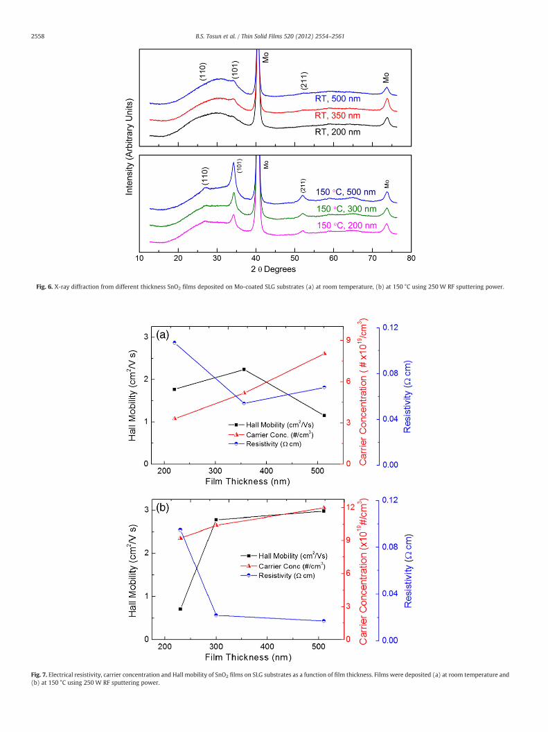
Fig. 6. X-ray diffraction from different thickness SnO2 films deposited on Mo-coated SLG substrates (a) at room temperature, (b) at 150 °C using 250 W RF sputtering power.
Fig. 7. Electrical resistivity, carrier concentration and Hall mobility of SnO2 films on SLG substrates as a function of film thickness. Films were deposited (a) at room temperature and(b) at 150 °C using 250 W RF sputtering power.
2558 B.S. Tosun et al. / Thin Solid Films 520 (2012) 2554–2561
2559B.S. Tosun et al. / Thin Solid Films 520 (2012) 2554–2561
The mobility in the film deposited at 150 °C is higher as expected.These trends are consisted with the XRD data shown in Fig. 6: thinnerfilms consist of nanocrystals embedded in amorphous SnO2 and mo-bility is approximately at 1–2 cm2/V s. In contrast at 150 °C, the mo-bility increases due to higher film crystallinity.
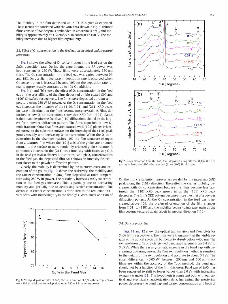
Fig. 9. X-ray diffraction from the SnO2 films deposited using different O2% in the feedgas (a) on Mo-coated SLG substrates and (b) on (100) Si substrates.
3.3. Effect of O2 concentration in the feed gas on electrical and structuralproperties
Fig. 8 shows the effect of O2 concentration in the feed gas on theSnO2 deposition rate. During the experiments, the RF power waskept constant at 250 W. These films were approximately 350 nmthick. The O2 concentration in the feed gas was varied between 0%and 15%. Only a slight decrease in deposition rate is observed whenO2 concentration is increased beyond 10% but the deposition rate re-mains approximately constant up to 10% O2 addition.
Fig. 9(a) and (b) shows the effect of O2 concentration in the feedgas on the crystallinity of the films deposited on Mo-coated SLG and(100) Si wafers, respectively. The films were deposited at room tem-perature using 250 W RF power. As the O2 concentration in the feedgas increases, the intensity of the (110), (101) and (211) XRD peaksincrease indicating that the films become more crystalline. Films de-posited at low O2 concentrations show that XRD from (101) planesis dominant despite the fact that (110) diffractions should be the larg-est for a powder diffraction pattern. The films deposited at low O2
mole fractions show that films are textured with (101) planes orient-ed normal to the substrate surface but the intensity of the (110) peakgrows steadily with increasing O2 concentration. When the O2 con-centration in the chamber reaches 10%, the film structure changesfrom a textured film where the [101] axis of the grains are orientednormal to the surface to more randomly oriented grain structure. Acontinuous increase in the (211) peak intensity with increasing O2%in the feed gas is also observed. In contrast, at high O2 concentrationsin the feed gas, the deposited film XRD shows an intensity distribu-tion closer to the powder diffraction pattern.
Clearly, the mobility is determined by the microstructure and ori-entation of the grains. Fig. 10 shows the resistivity, the mobility andthe carrier concentration in SnO2 films deposited at room tempera-ture using 250 W RF power. The resistivity increases as O2 concentra-tion in the feed gas increases. This is partially due to decreasingmobility and partially due to decreasing carrier concentration. Thedecrease in carrier concentration is attributed to the reduction in O-vacancies with increasing O2 in the feed gas. With small addition of
Fig. 8. Average deposition rates of SnO2 films as a function of O2% in the feed gas. Filmswere 350 nm thick and were deposited using 250 W RF sputtering power.
O2, the film crystallinity improves as revealed by the increasing XRDpeak along the (101) direction. Thereafter the carrier mobility de-creases with O2 concentration because the films become less tex-tured: the (110) XRD peak grows in as the (101) XRD peakdecreases. The film's XRD pattern becomes more like that of a powderdiffraction pattern. As the O2 concentration in the feed gas is in-creased above 10%, the preferred orientation of the film changesfrom (101) to (110) and the mobility begins to increase again as thefilm become textured again, albeit in another direction (110).
3.4. Optical properties
Figs. 11 and 12 show the optical transmission and Tauc plots forSnO2 films, respectively. The films were transparent in the visible re-gion of the optical spectrum but begin to absorb below ~400 nm. Theextrapolation of Tauc plots yielded band gaps ranging from 3.4 eV to3.65 eV. While there is a systematic increase in the band gap with de-creasing sputtering power, the Tauc extrapolation method is sensitiveto the details of the extrapolation and accurate to about 0.1 eV. Thesmall differences (~0.05 eV) between 200 nm and 500 nm thickfilms are within the accuracy of the Tauc method: the band gapshould not be a function of the film thickness. Band gap of SnO2 hasbeen suggested to shift to lower values than 3.6 eV with increasingoxygen vacancies [21]. This hypothesis is consistent both with our op-tical and electrical characterization data. Increasing the sputteringpower decreases the band gap and carrier concentration and both of

Fig. 10. The resistivity, the carrier concentration and the Hall mobility of SnO2 films on SLG substrates as a function of O2% in the feed gas.
2560 B.S. Tosun et al. / Thin Solid Films 520 (2012) 2554–2561
these effects have been hypothesized to be due to increasing oxygenvacancies in the film [8,21]. The index of refraction extracted from thevisible (500–700 nm) transmission using methods described in refer-ence 22 ranged between 1.8 and 1.9. This is slightly lower than theindex of refraction of bulk SnO2[22] and we attribute this lowervalue to internal voids, which were also observed in low-resolutionTEM images.
4. Conclusions
Sputtered SnO2 films become more crystalline with increasing RFpower, film thickness and substrate temperature. A small amount ofO2 (0.125%) in the feed gas also increases the crystallinity of thefilms. The SnO2 film electrical resistivity decreases with increasingRF power, film thickness and substrate temperature. The lowest resis-tivity, 8 mΩ cm, is achieved at 150 °C and using 250 W RF power in a500 nm thick film. The highest carrier concentration, 3.6×1020 cm−3,
Fig. 11. Optical transmission of nominally (a) 200 nm and (b) 500 nm th
is achieved with 250 W RF power and 150 °C substrate temperaturein 500 nm thick SnO2 films. A decrease in carrier concentration from1020 cm−3 to 1018 cm−3 is observed when O2 is added into thefeed gas. The carrier mobility of the films increases with increasingRF power, film thickness and substrate temperature. SemicrystallineSnO2 thin films can have mobilities of the order of 1–3 cm2/Vs. Thisis only slightly lower than the mobilities achieved in polycrystallineSnO2 and ZnO films (5–35 cm2/Vs) [23–27] and our highest crystal-linity films deposited by sputtering (6.8 cm2/Vs). We recentlyshowed that the semicrystalline films have superior water barrierproperties as compared to polycrystalline SnO2 and ZnO films. Wewere also able to assemble CIGS solar cells with semicrystaline SnO2
films with no sacrifice in the solar cell efficiency as compared tofilms made with polycrystalline ZnO: these results will be reportedelsewhere. Thus, while there is some sacrifice in the carrier mobilityof the semicrystalline SnO2 films in comparison to polycrystallineSnO2 and ZnO, it is not significant to cause degradation of device
ick SnO2 films sputtered at various RF powers at room temperature.
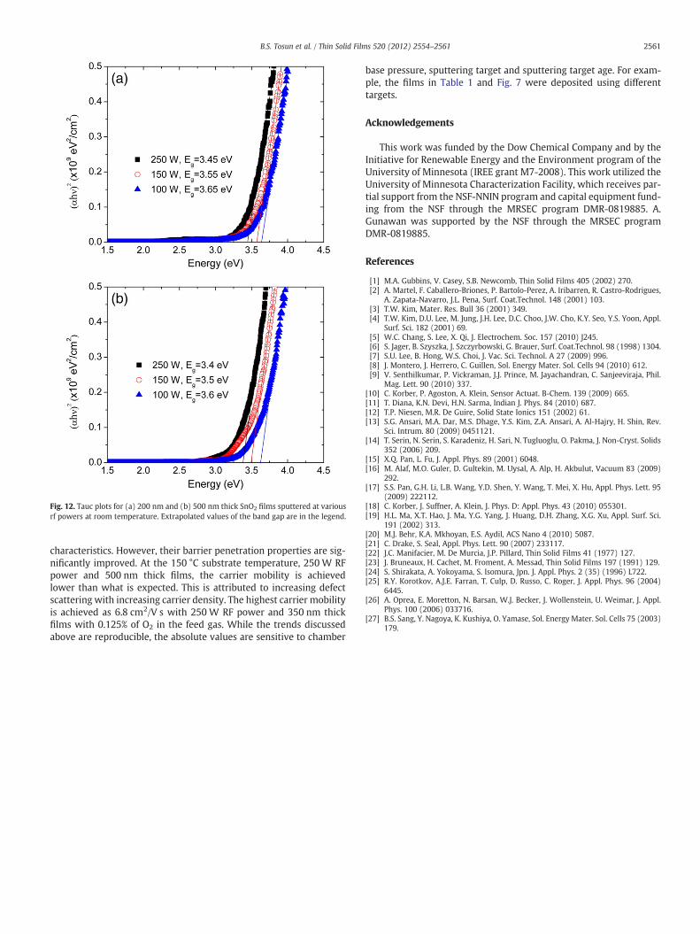
Fig. 12. Tauc plots for (a) 200 nm and (b) 500 nm thick SnO2 films sputtered at variousrf powers at room temperature. Extrapolated values of the band gap are in the legend.
2561B.S. Tosun et al. / Thin Solid Films 520 (2012) 2554–2561
characteristics. However, their barrier penetration properties are sig-nificantly improved. At the 150 °C substrate temperature, 250 W RFpower and 500 nm thick films, the carrier mobility is achievedlower than what is expected. This is attributed to increasing defectscattering with increasing carrier density. The highest carrier mobilityis achieved as 6.8 cm2/V s with 250 W RF power and 350 nm thickfilms with 0.125% of O2 in the feed gas. While the trends discussedabove are reproducible, the absolute values are sensitive to chamber
base pressure, sputtering target and sputtering target age. For exam-ple, the films in Table 1 and Fig. 7 were deposited using differenttargets.
Acknowledgements
This work was funded by the Dow Chemical Company and by theInitiative for Renewable Energy and the Environment program of theUniversity of Minnesota (IREE grant M7-2008). This work utilized theUniversity of Minnesota Characterization Facility, which receives par-tial support from the NSF-NNIN program and capital equipment fund-ing from the NSF through the MRSEC program DMR-0819885. A.Gunawan was supported by the NSF through the MRSEC programDMR-0819885.
References
[1] M.A. Gubbins, V. Casey, S.B. Newcomb, Thin Solid Films 405 (2002) 270.[2] A. Martel, F. Caballero-Briones, P. Bartolo-Perez, A. Iribarren, R. Castro-Rodrigues,
A. Zapata-Navarro, J.L. Pena, Surf. Coat.Technol. 148 (2001) 103.[3] T.W. Kim, Mater. Res. Bull 36 (2001) 349.[4] T.W. Kim, D.U. Lee, M. Jung, J.H. Lee, D.C. Choo, J.W. Cho, K.Y. Seo, Y.S. Yoon, Appl.
Surf. Sci. 182 (2001) 69.[5] W.C. Chang, S. Lee, X. Qi, J. Electrochem. Soc. 157 (2010) J245.[6] S. Jager, B. Szyszka, J. Szczyrbowski, G. Brauer, Surf. Coat.Technol. 98 (1998) 1304.[7] S.U. Lee, B. Hong, W.S. Choi, J. Vac. Sci. Technol. A 27 (2009) 996.[8] J. Montero, J. Herrero, C. Guillen, Sol. Energy Mater. Sol. Cells 94 (2010) 612.[9] V. Senthilkumar, P. Vickraman, J.J. Prince, M. Jayachandran, C. Sanjeeviraja, Phil.
Mag. Lett. 90 (2010) 337.[10] C. Korber, P. Agoston, A. Klein, Sensor Actuat. B-Chem. 139 (2009) 665.[11] T. Diana, K.N. Devi, H.N. Sarma, Indian J. Phys. 84 (2010) 687.[12] T.P. Niesen, M.R. De Guire, Solid State Ionics 151 (2002) 61.[13] S.G. Ansari, M.A. Dar, M.S. Dhage, Y.S. Kim, Z.A. Ansari, A. Al-Hajry, H. Shin, Rev.
Sci. Intrum. 80 (2009) 0451121.[14] T. Serin, N. Serin, S. Karadeniz, H. Sari, N. Tugluoglu, O. Pakma, J. Non-Cryst. Solids
352 (2006) 209.[15] X.Q. Pan, L. Fu, J. Appl. Phys. 89 (2001) 6048.[16] M. Alaf, M.O. Guler, D. Gultekin, M. Uysal, A. Alp, H. Akbulut, Vacuum 83 (2009)
292.[17] S.S. Pan, G.H. Li, L.B. Wang, Y.D. Shen, Y. Wang, T. Mei, X. Hu, Appl. Phys. Lett. 95
(2009) 222112.[18] C. Korber, J. Suffner, A. Klein, J. Phys. D: Appl. Phys. 43 (2010) 055301.[19] H.L. Ma, X.T. Hao, J. Ma, Y.G. Yang, J. Huang, D.H. Zhang, X.G. Xu, Appl. Surf. Sci.
191 (2002) 313.[20] M.J. Behr, K.A. Mkhoyan, E.S. Aydil, ACS Nano 4 (2010) 5087.[21] C. Drake, S. Seal, Appl. Phys. Lett. 90 (2007) 233117.[22] J.C. Manifacier, M. De Murcia, J.P. Pillard, Thin Solid Films 41 (1977) 127.[23] J. Bruneaux, H. Cachet, M. Froment, A. Messad, Thin Solid Films 197 (1991) 129.[24] S. Shirakata, A. Yokoyama, S. Isomura, Jpn. J. Appl. Phys. 2 (35) (1996) L722.[25] R.Y. Korotkov, A.J.E. Farran, T. Culp, D. Russo, C. Roger, J. Appl. Phys. 96 (2004)
6445.[26] A. Oprea, E. Moretton, N. Barsan, W.J. Becker, J. Wollenstein, U. Weimar, J. Appl.
Phys. 100 (2006) 033716.[27] B.S. Sang, Y. Nagoya, K. Kushiya, O. Yamase, Sol. Energy Mater. Sol. Cells 75 (2003)
179.