thesis internal data bus of a small student satellite
DESCRIPTION
Thesis about CubeSat platformTRANSCRIPT
Master of Science in ElectronicsJune 2011Bjørn B. Larsen, IET
Submission date:Supervisor:
Norwegian University of Science and TechnologyDepartment of Electronics and Telecommunications
Internal Data Bus of a Small StudentSatellite
Marius Lind Volstad


Problem description
In modern satellites, containing many separate digital systems, it is essentialfor the functionality of the satellite to allow for reliable and power efficientcommunication between all systems. The most effective way of ensuringsystem-to-system communication is through a common data bus. The inter-nal data bus will be the backbone of the satellite and has to remain operablethrough the lifespan of the satellite. It is also beneficial for the integrity ofthe satellite to have an On-Board Controller (OBC) to log useful data andmonitor the digital systems.
The student shall design a reliable data bus and OBC for use in theNTNU Test Satellite (NUTS) project.
Assignment Given: 24.01.2011Supervisor: Bjørn B. LarsenCo-supervisor: Roger Birkeland
i

ii
Abstract
This thesis presents a platform for a small student satellite. A backplanesolution with slots for 8 individual modules is proposed. The backplane pro-vides the modules with power and a common data bus, as well as mechanismsfor isolating modules from the rest of the system and a possibility of restoringmisbehaving modules. It has a power consumption of about 100mW.
An on-board controller has been designed and tested. It consists of a32-bit MCU, a NAND flash memory for housekeeping logs, an SRAM mem-ory for processing variables, an OTP memory for safe storage of modulefirmwares, USB interface and a wireless intra-satellite communication mod-ule. The on-board controller has the main responsibility for monitoring andpreserving the satellite’s health. The power consumption will be dependentof the final firmware, but a rough estimate is about 100mW.
Also, an experimental wireless intra-satellite communication system isproposed. The system consists of a small wireless module, that will be inte-grated onto any module that is a part of the wireless network.
iii

iv

Preface
My first thought when joining the NUTS project, was that it would be ex-tremely satisfying building something that is destined to be launched intospace. But I felt a bit confused after the first introductory speeches of whatbuilding a satellite was all about. There were a lot of new concepts andmethodologies to become familiar with. After some time immersing myselfin space and satellite related material, I again began to feel the excitementof being a part of a team of satellite builders.
The work with the backplane has been a joint effort by Dewald de Bruynand myself. Dewald has had main responsibility for the power solution anddone most of the hardware layout drawings, while I have made the digitalsystems. We have had many discussions about the system, and feel that wehave ended up with a solid design.
It has been incredibly educational to work with the NUTS project. I havemet many challenges and felt a lot of joy in overcoming the obstacles. Also,I have had the pleasure of being a part of a very competent team. And now,I’m looking forward to coming back to NTNU for the launch of NTNU’s firstsuccessful satellite mission!
———————————————————-
Marius Lind Volstad
v

vi

Acknowledgement
I would like to thank my supervisors Bjørn B. Larsen and Roger Birkelandfor guidance on this thesis, and thanks to Dewald de Bruyn for coopera-tion during the backplane development. Thanks to Torbjørn Finnøy, DanielAasbø, Kjetil Kvalø and Carolina Fiorella Inche Velezmoro for overall helpwith this thesis and great company at the office. A double thanks to DanielAasbø for corrective reading of the thesis.
vii

viii

Contents
Abstract iii
Preface v
Acknowledgement vii
Contents ix
Acronyms xiii
List of Figures xv
List of Tables xvii
1 Introduction 11.1 Internal Communication . . . . . . . . . . . . . . . . . . . . . 21.2 Backplane . . . . . . . . . . . . . . . . . . . . . . . . . . . . . 21.3 On-Board Controller . . . . . . . . . . . . . . . . . . . . . . . 2
2 Background Information and Theory 32.1 The Space Environment . . . . . . . . . . . . . . . . . . . . . 3
2.1.1 Space Radiation . . . . . . . . . . . . . . . . . . . . . . 32.1.2 Vacuum Conciderations . . . . . . . . . . . . . . . . . 82.1.3 Space Debris . . . . . . . . . . . . . . . . . . . . . . . 8
2.2 Memory . . . . . . . . . . . . . . . . . . . . . . . . . . . . . . 92.2.1 NAND Flash . . . . . . . . . . . . . . . . . . . . . . . 92.2.2 Static Random Access Memory . . . . . . . . . . . . . 102.2.3 One-Time-Programmable Memory . . . . . . . . . . . . 10
ix
Contents
2.3 Digital Logic Series . . . . . . . . . . . . . . . . . . . . . . . . 112.4 AT32UC3A3 . . . . . . . . . . . . . . . . . . . . . . . . . . . . 112.5 nRF24LE1 . . . . . . . . . . . . . . . . . . . . . . . . . . . . . 12
3 Backplane 133.1 Design . . . . . . . . . . . . . . . . . . . . . . . . . . . . . . . 16
3.1.1 Data Bus . . . . . . . . . . . . . . . . . . . . . . . . . 163.1.2 Power System . . . . . . . . . . . . . . . . . . . . . . . 193.1.3 Digital Control . . . . . . . . . . . . . . . . . . . . . . 203.1.4 Mechanical Considerations . . . . . . . . . . . . . . . . 243.1.5 System Overview . . . . . . . . . . . . . . . . . . . . . 25
3.2 Prototyping . . . . . . . . . . . . . . . . . . . . . . . . . . . . 253.2.1 Testing . . . . . . . . . . . . . . . . . . . . . . . . . . . 253.2.2 Results . . . . . . . . . . . . . . . . . . . . . . . . . . . 29
4 On-Board Controller 314.1 Hardware Design . . . . . . . . . . . . . . . . . . . . . . . . . 31
4.1.1 Microcontroller . . . . . . . . . . . . . . . . . . . . . . 324.1.2 Memory Hierarchy . . . . . . . . . . . . . . . . . . . . 324.1.3 Backplane Connector . . . . . . . . . . . . . . . . . . . 334.1.4 USB Interface . . . . . . . . . . . . . . . . . . . . . . . 344.1.5 Manual Override . . . . . . . . . . . . . . . . . . . . . 344.1.6 Hardware Overview . . . . . . . . . . . . . . . . . . . . 34
4.2 Software Design . . . . . . . . . . . . . . . . . . . . . . . . . . 354.2.1 Drivers . . . . . . . . . . . . . . . . . . . . . . . . . . . 354.2.2 Housekeeping . . . . . . . . . . . . . . . . . . . . . . . 364.2.3 Operating System . . . . . . . . . . . . . . . . . . . . . 364.2.4 Support Software . . . . . . . . . . . . . . . . . . . . . 36
4.3 Prototyping . . . . . . . . . . . . . . . . . . . . . . . . . . . . 374.3.1 Testing . . . . . . . . . . . . . . . . . . . . . . . . . . . 374.3.2 Results . . . . . . . . . . . . . . . . . . . . . . . . . . . 38
5 Internal Wireless Communication 415.1 Hardware Design . . . . . . . . . . . . . . . . . . . . . . . . . 425.2 Firmware Design . . . . . . . . . . . . . . . . . . . . . . . . . 43
5.2.1 Protocol . . . . . . . . . . . . . . . . . . . . . . . . . . 435.3 Prototyping . . . . . . . . . . . . . . . . . . . . . . . . . . . . 46
5.3.1 Testing . . . . . . . . . . . . . . . . . . . . . . . . . . . 47
x
Contents
5.3.2 Results . . . . . . . . . . . . . . . . . . . . . . . . . . . 47
6 Discussion 49
7 Concluding Remarks 53
8 Future Work 558.1 Wireless link . . . . . . . . . . . . . . . . . . . . . . . . . . . . 558.2 OBC Completion . . . . . . . . . . . . . . . . . . . . . . . . . 558.3 Radiation Detector . . . . . . . . . . . . . . . . . . . . . . . . 55
Bibliography 57
A Backplane 59
B On-Board Controller 71
C Wireless Internal Communication Module 75
xi

xii

Acronyms
ADC Analog-to-Digital Converter.
CAN Controller Area Network.
CD Compact Disc.
CMOS Complementary Metal-Oxide-Semiconductor.
DMIPS Dhrystone Million Instructions Per Second
(MIPS).
DSP Digital Signal Processing.
ECC Error Correcting Code.
GPIO General Purpose Input/Output.
GUI Graphical User Interface.
I2C Inter-Integrated Circuit.
IC Integrated Circuit.
LEO Low Earth Orbit.
MCU Microcontroller Unit.
MeV Megaelectronvolt.
xiii

Acronyms
MIPS Million Instructions Per Second.
MOS Metal Oxide Semiconductor.
NUTS NTNU Test Satellite.
OBC On-Board Controller.
OTP One-Time Programmable.
PCB Printed Circuit Board.
RAM Random Access Memory.
SCL Serial Clock Line.
SDA Serial Data Line.
SEE Single Event Effect.
SEU Single Event Upset.
SOI Silicon-On-Insulator.
SPI Serial Peripheral Interface.
SRAM Static RAM.
TID Total Ionizing Dose.
UART Universal Asynchronous Receiver/Transmit-
ter.
USB Universal Serial Bus.
xiv

List of Figures
2.1 Illustration of the Van Allen belts. Courtesy of NASA. . . . . 42.2 A standard CMOS inverter with parasitic transistors. Cour-
tesy of Aerospace Corporation. . . . . . . . . . . . . . . . . . . 52.3 A majority voting system, processor 2 is defective. . . . . . . . 72.4 A majority voting system with time delay. . . . . . . . . . . . 72.5 The floating gate transistor. . . . . . . . . . . . . . . . . . . . 92.6 An SRAM memory cell. . . . . . . . . . . . . . . . . . . . . . 10
3.1 The centralized system solution. . . . . . . . . . . . . . . . . . 143.2 The distributed system solution. . . . . . . . . . . . . . . . . . 143.3 An illustration of a backplane solution, from the NUTS-1 Mis-
sion Statement. . . . . . . . . . . . . . . . . . . . . . . . . . . 153.4 The proposed bus topology. . . . . . . . . . . . . . . . . . . . 183.5 The satellite power system. . . . . . . . . . . . . . . . . . . . . 193.6 The address matching circuit for the module controls. . . . . . 203.7 Power and data bus access control. . . . . . . . . . . . . . . . 213.8 Control waveform for power and data bus access flip-flops. . . 223.9 The backplane reset circuitry. . . . . . . . . . . . . . . . . . . 223.10 The backplane reprogramming circuitry. . . . . . . . . . . . . 233.11 The module to backplane connector. . . . . . . . . . . . . . . 243.12 An overview of the backplane, excluding control logic. . . . . . 263.13 Pinouts for master slots (left), payload slots (middle) and
power slot (right). . . . . . . . . . . . . . . . . . . . . . . . . . 273.14 The circuit board for the backplane. . . . . . . . . . . . . . . . 273.15 The finished backplane with On-Board Controller (OBC) mod-
ule. . . . . . . . . . . . . . . . . . . . . . . . . . . . . . . . . . 28
4.1 A system overview of the OBC. . . . . . . . . . . . . . . . . . 34
xv

List of Figures
4.2 The circuit board for the OBC. . . . . . . . . . . . . . . . . . 374.3 The finished OBC. . . . . . . . . . . . . . . . . . . . . . . . . 38
5.1 An overview of the wireless transceiver module. . . . . . . . . 425.2 The wireless module circuit board. Top view on the left, and
bottom view on the right. . . . . . . . . . . . . . . . . . . . . 465.3 The wireless module. . . . . . . . . . . . . . . . . . . . . . . . 46
A.1 Backplane schematic, page 1. . . . . . . . . . . . . . . . . . . 60A.2 Backplane schematic, page 2. . . . . . . . . . . . . . . . . . . 61A.3 Backplane schematic, page 3. . . . . . . . . . . . . . . . . . . 62A.4 Backplane schematic, page 4. . . . . . . . . . . . . . . . . . . 63A.5 Backplane schematic, page 5. . . . . . . . . . . . . . . . . . . 64A.6 Backplane schematic, page 6. . . . . . . . . . . . . . . . . . . 65A.7 Backplane schematic, page 7. . . . . . . . . . . . . . . . . . . 66A.8 Backplane schematic, page 8. . . . . . . . . . . . . . . . . . . 67A.9 Backplane schematic, page 9. . . . . . . . . . . . . . . . . . . 68A.10 Backplane schematic, page 10. . . . . . . . . . . . . . . . . . . 69A.11 Backplane schematic, page 11. . . . . . . . . . . . . . . . . . . 70
B.1 On-Board Controller schematic, page 1. . . . . . . . . . . . . . 72B.2 On-Board Controller schematic, page 2. . . . . . . . . . . . . . 73
C.1 Intra-satellite Communication Module schematic. . . . . . . . 76
xvi
List of Tables
2.1 Estimated amount of space debris. Source: American Instituteof Physics. . . . . . . . . . . . . . . . . . . . . . . . . . . . . . 8
3.1 Selected data bus characteristics based on common specifica-tions. . . . . . . . . . . . . . . . . . . . . . . . . . . . . . . . . 17
3.2 Testing specification of the backplane. . . . . . . . . . . . . . 28
5.1 Example address table for wireless transmission. . . . . . . . . 445.2 A transmission from Module A to Module B. . . . . . . . . . . 455.3 Dividing the channel controls in time for each link. . . . . . . 45
xvii

xviii

Chapter 1
Introduction
This thesis is one of many concerning the student satellite program at NTNU,called NTNU Test Satellite (NUTS). A document outlining the mission ob-jectives for NUTS is attached on the accompanying Compact Disc (CD). Ashort summary of the mission objectives is given below:
The NUTS (NTNU Test Satellite) project was started in Septem-ber 2010. The project is part of the Norwegian student satelliteprogram run by NAROM (Norwegian Centre for Space-related Ed-ucation). The projects goal is to design, manufacture and launcha double CubeSat by 2014. The national student satellite programinvolves three educational establishments, namely the University ofOslo (UiO), Narvik University College (HiN) and NTNU.
As main payload, the NUTS project will fly an IR-camera for at-mospheric observations. In addition, a concept for a wireless shortrange data bus connecting different subsystems will be added. Forcommunication, the satellite will use the common amateur radiobands and fly one transceiver for each frequency. During the firsthalf of 2011, ten students from different departments and curricu-lums were involved in the project.
It has previously been done research on building a student satellite atNTNU. This research stems from both previous projects, and a precursory
1

Chapter 1. Introduction
study for the NUTS project. Some previous experiences have been incorpo-rated into the research.
The NUTS will be orbiting Earth way out of reach for us to do anyphysical maintenance after launch. It is also too far out to be protected fromsolar radiation by our planet’s atmosphere. Because of this, it is extremelyimportant that the satellite is designed to be self-reliant and robust. Thereare many aspects to consider to design such a system. This thesis focuses onthree main points; the internal communication, providing a systems platformfor maximum lifespan and an OBC.
1.1 Internal Communication
The internal communication of the satellite will consist of a regular wired busfor main internal communication, and an experimental wireless bus. Wirelessintra-satellite communication has not yet been widely tested, and one of themission objectives is therefore to test if this is a viable replacement.
1.2 Backplane
The basic platform of the satellite is refered to as the backplane. It willconsist of all the necessary circuitry for providing power and communicationsto the payloads, and also for isolating and restoring misbehaving sub-systems.In short terms; it is the connection hub for all sub-systems.
1.3 On-Board Controller
An OBC is responsible for much of the housekeeping of the satellite. It hasthe main responsibility for monitoring the health of the system, and to takeany necessary actions. It should keep a log of all events and vital missiondata, and be able to offer processing capabilities for other systems.
The accompanying CD contains developed code, as well as source files forschematics and layout.
2

Chapter 2
Background Information andTheory
This chapter will present various theory and concepts useful for understand-ing the rest of this thesis. Some electronic devices used are also presented.
2.1 The Space Environment
The environment in space is very different from the normal operating con-ditions of electronic devices. This section will outline these differences, andreflect on the difficulties they pose.
2.1.1 Space Radiation
Space radiation is one of the biggest concerns when dealing with satellitesin orbit. It consists of high energy particles radiated from several sourcesin space. [1] These particles comes from cosmic rays, as well as our ownsun. Cosmic rays mainly consists of the nuclei of a variety of atoms, but alsoincludes subatomic particles such as positrons and electrons.[2] Other stars,novas, supernovas and other objects are responsible for the cosmic rays. Theradiation from the sun mostly stems from the fusion processes in the core,which results in a solar wind of electrons and protons. The strength of the
3

Chapter 2. Background Information and Theory
Figure 2.1: Illustration of the Van Allen belts. Courtesy of NASA.
solar radiation will vary with the sunspot activity, and will peak during solarflares.
When the radiation reaches Earth, it will be affected by Earth’s electro-magnetic field. This will cause some of the radiation to accumulate in theupper atmosphere in what is called the Van Allen Radiations belts. There aretwo belts, the inner and the outer belt. The inner belt mostly consist of pro-tons with energy above 3 Megaelectronvolt (MeV). The outer belt containsless energetic protons, but has electrons that can have energies of severalhundred MeV. [3] The inner Van Allen belt has its centre at approximately2,000 km above the surface of the Earth. However, measurements have shownthat the belt is descending closer to the poles, and that the radiation canhave considerable concentrations at lower altitudes. An illustration of theVan Allen belts are shown in figure 2.1.
Effects of Radiation on Electronic Components
The bombardment of highly energetic space radiation can cause some trou-bling effects on electronic components. The total radiation dose will leadto a constant degradation of the components, and will eventually cause thedevice to fail. In addition, the radiation can cause spontaneous Single EventEffects (SEEs). Radiation in the form of protons or heavy ions will releaseenergy by ionization when it penetrates the components. The ionization willgive a charge at the node, and lead to a short current pulse.
4

2.1. The Space Environment
Figure 2.2: A standard CMOS inverter with parasitic transistors. Courtesyof Aerospace Corporation.
Latch-up is a state found in Complementary Metal-Oxide-Semiconductor(CMOS) devices where a high current moves from the component’s sourcevoltage to ground. In this state, the component will not respond properlyto input stimuli. [4] Normal operation can be restored by removing andreapplying power, but heat dissiapation from the current flow might havedestroyed the component.
The problem can be understood by considering the standard CMOS logicinverter seen in figure 2.2. The die has a PNPN-structure which results in theequivalent circuit of two connected transistors. When high energy radiationpenetrates into this structure and releases some of it’s energy as a currentspike, it can activate one of the transistors. The current consumption willincrease due to positive feedback in the circuit, and ultimately become ashort-circuit. [5]
A Single Event Upset (SEU) is a less devastating effect, but can stillcause mayhem on the circuit’s operation. Consider a storage element suchas a flip-flop, NAND flash or SRAM cell. A heavy ion can penetrate into thestructure and leave a charge that flips one or more bits. The consequence
5

Chapter 2. Background Information and Theory
of this SEE will depend on the application’s interpretation of the specificbits, but could possibly be mission-threatening if it affects e.g. navigation orpower controls.
Total Ionizing Dose (TID) refers to the amount of ionizing radiationa component has accummulated over time. The ionizing radiation leadsto a change in the physical parameters of the devices. More specifically itwill result in a shift of the threshold voltage of Metal Oxide Semiconductor(MOS) transistors. [6] This could lead to a higher leakage current, andeventual failure of the electronic components.
Improving Radiation Tolerance
Physically shielding by encapsulating the sensitive components in a radi-ation absorbing or reflecting material is possible. Depending on the materialcharacteristics and thickness it will reduce the amount of radiation reach-ing the components. However, the shielding will not be able to stop all theradiation, and especially not the most energetic particles that causes SEEs.
Fabrication processes exists that can be used to counteract latch-up.Latch-up is dependent on the existence of the PNPN-structure. For themost common CMOS fabrication process this structure will be present onnumerous places. Luckily, there are design methods and alternate fabricationprocesses to counter the PNPN-structure. [7] One design method is to disruptthe current flow path by placing an n-well contact to the power supply foreach pFET connected to the power supply. [4] An example for latch-uptolerant processes is the Silicon-On-Insulator (SOI) process. SOI builds it’stransistors on an insulator instead of a silicon substrate. This won’t lead tothe formation of the PNPN-structure.
Redundancy is a way of increasing the reliability of a system by du-plicating sub-systems or information. This is especially important in spaceapplications, where the equipment is constantly subject to a bombardmentof radiation, which results in SEUs and degradation. However, redundancywill add some extra space and complexity to both hardware and software.
Error Correcting Codes (ECCs) will assure data integrity by addingredundant bits to a bulk of data. [8] These bits are calculated using specialalgorithms to allow for detection and even correction of bit errors. There are
6
2.1. The Space Environment
Majority Voter
Processor 1
Processor 2
Processor 3
0xAA
0xA9
0xAA
Output: 0xAA Input: 0x55
Figure 2.3: A majority voting system, processor 2 is defective.
Majority Voter
Processor 1
Processor 2
Processor 3
0xA4
0xAA
0xAA
Output: 0xAA Input: 0x551us
2us
1us
2us
Figure 2.4: A majority voting system with time delay.
a number of different algorithms such as Hamming codes and Reed Solomoncodes, which vary in calculation complexity and storage efficiency (i.e. howmany bits are redundant). Some Microcontroller Units (MCUs) have inte-grated generators for some codes, which will heavily increase the throughput.
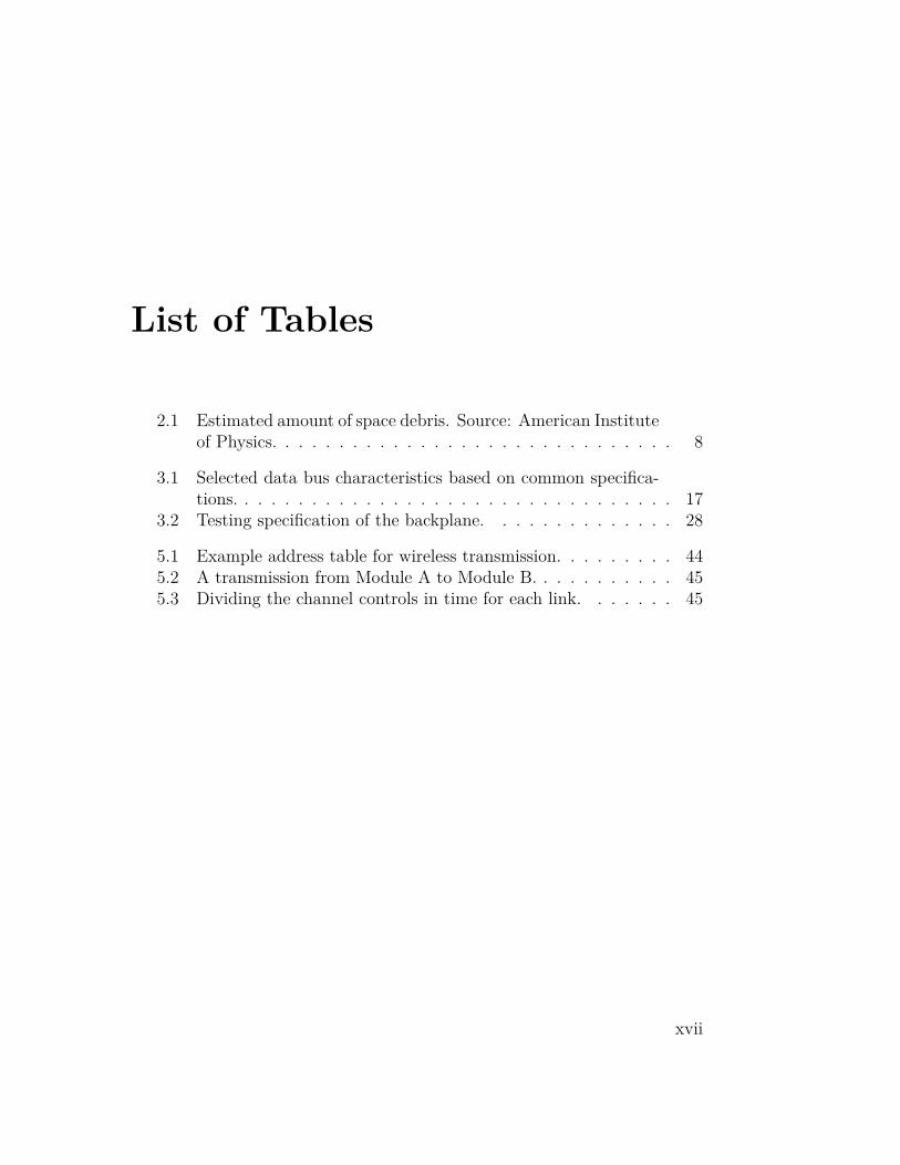
Majority voting is useful when adding redundant duplicated pieces ofhardware for processing. It is used to decide which result is the correct one,and which sub-systems have been damaged and produces the faulty response.This can be done by majority voting where the result from all the redundantsystems are compared, and the most common answer will be assumed to becorrect. Figure 2.3 shows a system using majority voting.
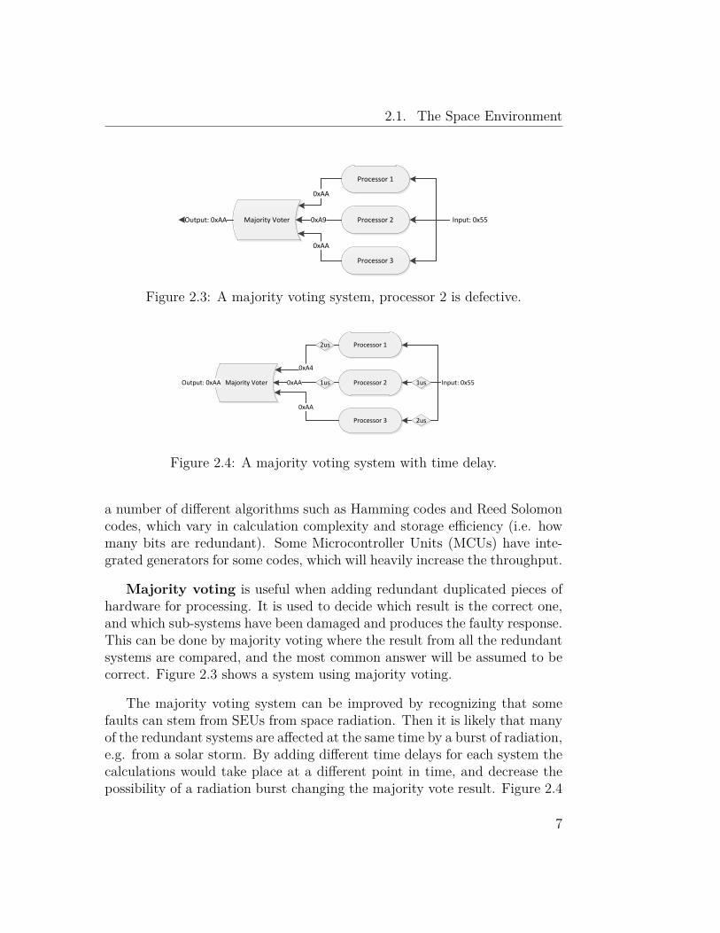
The majority voting system can be improved by recognizing that somefaults can stem from SEUs from space radiation. Then it is likely that manyof the redundant systems are affected at the same time by a burst of radiation,e.g. from a solar storm. By adding different time delays for each system thecalculations would take place at a different point in time, and decrease thepossibility of a radiation burst changing the majority vote result. Figure 2.4
7
Chapter 2. Background Information and Theory
shows the majority voting system with time delay implemented.
2.1.2 Vacuum Conciderations
The concentration of particles of the atmosphere in Low Earth Orbit (LEO)is significantly smaller than on the surface of Earth. Since the atmosphereexcert a pressure depending on the concentration of particles, the pressureis much higher on the surface. [9] Certain conciderations must be taken inorder for the pressure difference of the design environment, the surface ofEarth, and the flight environment, LEO, to not have a damaging effect. Ifbubbles of gas and liquid have been trapped in any component package ora Printed Circuit Board (PCB), it could lead to the pressure damaging thematerial and possibly the whole component or PCB.
Such bubbles can occur on a PCB during manufacturing if a via holeis buried between copper layers or solder mask. And even during solderingpockets of gas or liquids can be trapped in the solder. The components canalso contain pockets from the packaging process. A danger also arises if anyof these gases or liquids are acidic, which could result in damage to the wholesatellite or even other satellites in the same rocket.
2.1.3 Space Debris
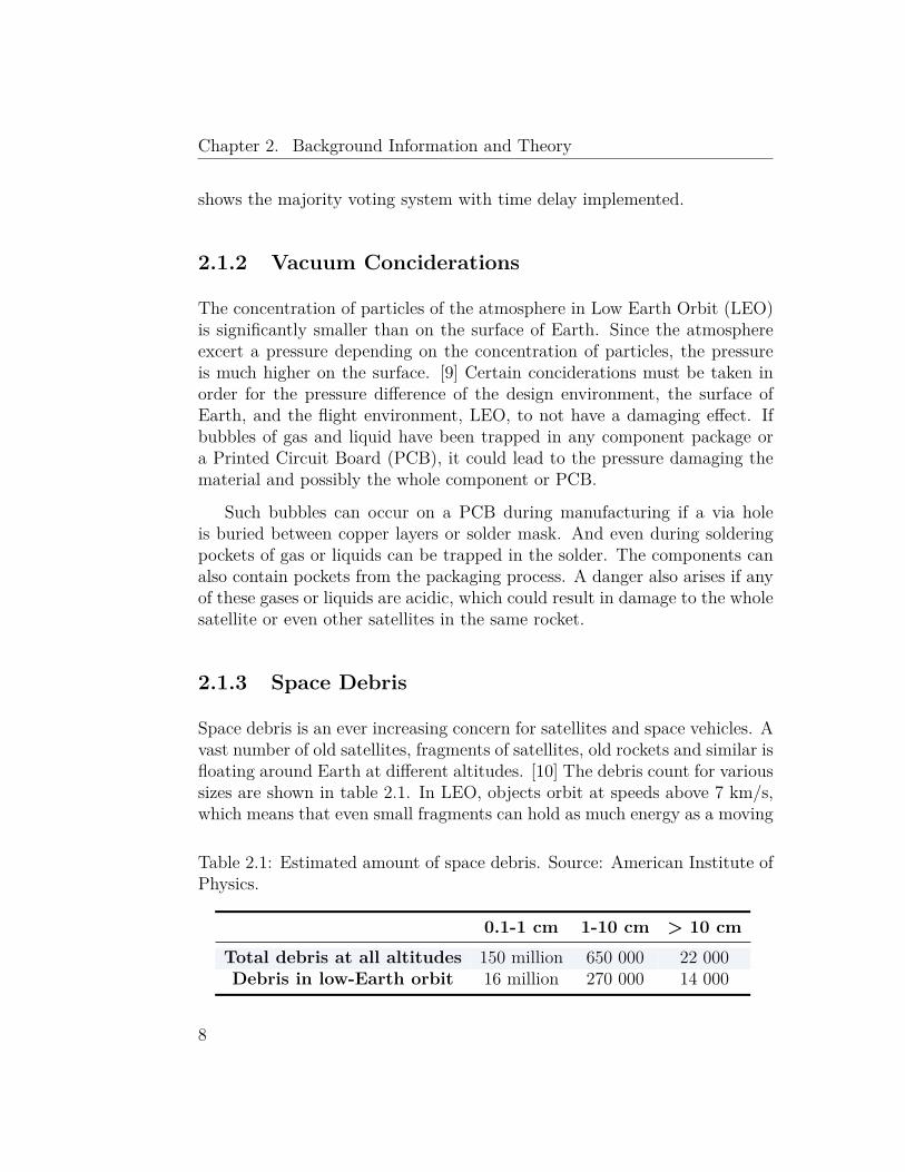
Space debris is an ever increasing concern for satellites and space vehicles. Avast number of old satellites, fragments of satellites, old rockets and similar isfloating around Earth at different altitudes. [10] The debris count for varioussizes are shown in table 2.1. In LEO, objects orbit at speeds above 7 km/s,which means that even small fragments can hold as much energy as a moving
Table 2.1: Estimated amount of space debris. Source: American Institute ofPhysics.
0.1-1 cm 1-10 cm > 10 cmTotal debris at all altitudes 150 million 650 000 22 000Debris in low-Earth orbit 16 million 270 000 14 000
8

2.2. Memory
n+ n+
Floating gate
Control gate
Source Drain
Figure 2.5: The floating gate transistor.
car on the freeway. All fragments between 1 mm and 1 cm are considered topose a threat to satellites, while any fragment above 1 cm would definitelydestroy it.
The only way to improve space debris resilience would be to shield thesatellite with durable materials. This would make the satellite too heavy tofit into the CubeSat standards. Luckily, there is a vast amount of space andthe chance of a collision is small, even though the possibility of a collision isreal.
2.2 Memory
Memory devices are an indispensable part of all advanced systems, and arepresent in some form. This section will give a brief introduction to sometypes used in this thesis.
2.2.1 NAND Flash
NAND Flash storage devices are based on a floating gate MOS transistor. [11]A floating gate transistor can be thought of as a regular MOS transistor withan extra control gate on top of the normal gate, as illustrated in figure 2.5.A charge can be built up on the floating gate, which will hold the transistorin it’s on or off state. The state of the transistor decides if a one or a zerois stored in the cell. The process of depositing charge on the floating gatevaries among technologies and manufacturers. But one way of programmingis to ground the P-substrate and N-well, and then applying voltage to the
9

Chapter 2. Background Information and Theory
WLnBit Bit
Figure 2.6: An SRAM memory cell.
control gate. This will create an electric field that pulls electrons onto thefloating gate, making it negatively charged. The floating gate is chargedpositively by applying ground to the control gate and voltage to the sourceof the transistor.
2.2.2 Static Random Access Memory
A Static RAM (SRAM) memory cell is based on two connected transistorinverters, as shown in figure 2.6. [12] The inverters will keep the gate voltageof each other to retain the bit information. Reading is performed by acti-vating the control transistors, which connects the inverters to the bit lines.Write is performed in the same way, but by applying the new bit on the bitline and thereby charging or discharging the gate.
2.2.3 One-Time-Programmable Memory
The One-Time Programmable (OTP) memory is a non-volatile memory thatcan only be programmed once. It is built up by an array of fuses thatis permanently broken during programming. [13] There are many differentconfigurations of OTP memory, but the basic principles are the same. Pro-gramming is performed by imposing a large enough current or voltage todamage the dielectric material. [14] Address lines are available to address
10
2.3. Digital Logic Series
specific parts of the memory. Information is then stored by addressing thecorrect part and programming the fuses that should be programmed.
Since information is stored by structurally altering the component, itis considered to be more reliable than other memories in harsh radiationenvironments. In fact, certain technologies of OTP memories has provento be specifically radiation tolerant. The resistance of a programmed OTPantifuse memory cell based on amorphous silicon is not affected by radiation,and the resistance of an unprogrammed cell will increase under radiation, i.e.improve. [15]
2.3 Digital Logic Series
Using digital logic is not as simple as just selecting the logic expression youwant to realize and putting it together using the available Integrated Circuits(ICs). There are several key parameters to take into concideration, such asvoltage levels, power consumption, speed and other internal aspects of thelogic circuitry. For example a logic device that supports partial power downwill not be partially powered through an I/O pin when it’s power supplyhas been shut off. There are dozens of different families and technologies ofdigital logic to explore. [16]
2.4 AT32UC3A3
The AT32UC3A3 is a range of MCU devices built around the AVR32 corefrom Atmel. [17] It offers 32 bit processing at up to 92 Dhrystone MIPS(DMIPS), and a Digital Signal Processing (DSP) instruction set. It can han-dle many memory interfaces automatically, and supports multiple differentmemory devices connected to a common bus at the same time. The memoryinterface can be used together with an ECC generator to add redundancy. AUniversal Serial Bus (USB) interface is available for connectivity to a com-puter.
11

Chapter 2. Background Information and Theory
2.5 nRF24LE1
The nRF24LE1 is a combination of a 2.4GHz radio transceiver and an 8051MCU from Nordic. [18] It can transfer data at a maximum rate of 2Mbps,but can be lowered to acheive a better transmission reliability. The MCUoffers several modules such as communication, encryption and Analog-to-Digital Converter (ADC). An external crystal can be connected to providea low-power synchronization clock. Both the radio and the MCU has beenoptimized to be power efficient.
An OTP edition of nRF24LE1 is available. This version provides an OTPmemory instead of the normal flash for firmware storage. In addition, someOTP memory is also available for storing data.
12
Chapter 3
Backplane
A system as complicated as a satellite will always be divided into severalsub-systems. The designers working on those sub-systems will focus on com-pleting their specific task. But eventually all the sepearate sub-systems hasto be sown together into the completed satellite. So the question is; how willeverything be tied together?
There are ultimately two main topologies for connecting the sub-systemstogether. A centralized approach, as shown in figure 3.1, will consist of amain computer functioning as the connection point between all sub-systems.The distributed system, shown in figure 3.2, consists of a common connectionlink shared by all sub-systems. Previous research on the subject has favoredthe distributed system because of reusability and scalability. [19] Scalabilityis important because the designer of the data bus-system does not necessarilyknow in what way the data bus will be used.
The use of a distributed system makes it much easier to define a commonconnector and pin-out for all sub-systems in the satellite. This introduces thethought of a backplane. A backplane is a board with several connectors thatinterfaces the sub-systems together. An illustration of the general thoughtof the backplane is shown in figure 3.3. The different sub-systems are thenbuilt as separate modules that fits directly onto the backplane connector.This solution makes it easy for designers to insert and remove single cardswithout having to dismantle the whole satellite every time a change must bemade.
13

Chapter 3. Backplane
Main MCU
Payload
Payload
Payload
Payload
Payload
Payload
Payload
Payload
Figure 3.1: The centralized system solution.
Main MCU
Payload Payload Payload
PayloadPayload
Payload
Payload Payload
Figure 3.2: The distributed system solution.
14

Figure 3.3: An illustration of a backplane solution, from the NUTS-1 MissionStatement.
15

Chapter 3. Backplane
The backplane will have slots for 8 modules. Two of them will be reservedas extended functionality master module slots, one for a special purposepower module and the remaining five as regular payload slots. The twomasters will be responsible for controlling most of the digital systems on thebackplane, and do general housekeeping in the satellite. Both masters willhave equal access to do everything, as a redundancy.
But there are still many considerations to be made. What if a modulestarts misbehaving and floods the data bus? Due to space radiation thisis likely to occur eventually during the satellite’s lifespan. There shouldbe some mechanisms for detecting the misbehaving module, isolating it andhopefully correcting the error. This makes it necessary to add control logic tothe backplane. The following section (3.1) presents a viable design solution.
3.1 Design
3.1.1 Data Bus
The data bus will be the main communication channel between all modules.It needs to be scalable and robust, provide a relatively high throughput rateand preferably have a low power consumption. In addition, it should beeasy to use for the modules, and the best way to assure this is to select acommonly available standard for the data bus. There are many differentstandards available, both for serial and parallell communication. Parallellbusses will require a much larger connector than the serial busses, thereforea serial interface is to prefer.
Many MCUs have integrated logic to automatically handle a range of com-munication protocols. Among the serial interfaces, the most found includesInter-Integrated Circuit (I2C), Serial Peripheral Interface (SPI), UniversalAsynchronous Receiver/Transmitter (UART) and Controller Area Network(CAN). The most important characteristics of each bus is summarized intable 3.1.
16
3.1. Design
Table 3.1: Selected data bus characteristics based on common specifications.
Data Bus Speed Lines NotesSPI 20Mbps 4 One chip select for each device.I2C 400kbps 2 Limited address and bus capacity.CAN 1Mbps 2 Needs external circuitry. Noise resilient.UART 1Mbps 2 Difficult to use between multiple nodes.
The most important aspects for the backplane is that the data bus shouldbe equally available for all and be as simple as possible. This excludes SPIbecause it requires a master device to control the chip select signal, or somesort of complex logic to control the arbitration process. UART will also re-quire som complex logic for arbitration since it is made for communicationbetween just two modules. The CAN bus would have been a good choice be-cause of it’s noise resilience, but most MCUs do not have integrated support.It would therefore be necessary to add some extra circuitry, and increase theoverall design complexity.
I2C
The I2C bus was selected as a common data bus. It is a very common databus with integrated support in most MCUs, and many sensor chips uses thisinterface. The bus only requires two lines for communication; Serial DataLine (SDA) and Serial Clock Line (SCL). [20] The lines are controlled byopen-collector logic, and pulled up to logic 1 by resistors in the idle state.This makes it possible to have multiple masters on the same bus, and im-plement collision detection and arbitration in software if there isn’t alreadysupported in hardware.
All devices are connected to these common lines, and addressed by aunique address for each device. The address space is limited to 7 bits giving128 possible addresses, but a 10 bit addressing mode can be used if necessary.Some of the addresses are reserved for specific purposes, so the true numberof available addresses is smaller depending on what devices are used. Therewill anyways be enough addresses for many modules and sensors connectedto the bus. If more devices are needed there exists an abundance of I2C
17

Chapter 3. Backplane
Module 1
Module 2
Module 3
Module 4
Module 5
Module 6
Module 7
Module 8
I2CRep.
I2CRep.
I2CRep.
I2CRep.
I2CRep.
I2CRep.
I2CRep.
I2CRep.
I2CBus
Figure 3.4: The proposed bus topology.
switches, multiplexers and hubs that can be used to create sub-domains ofthe I2C address space.
The total bus capacitance of the I2C bus will limit both the number ofdevices that can be connected to the bus and the total length of the bus. Thiscan be solved by using I2C repeaters that replicates the bus conditions onboth sides, acting like a buffer. These repeaters also have an enable/disablepin for connecting or disconnecting the two sides of the repeater, makingthem ideal for isolating malfunctioning devices from the bus.
Bus Topology
The bus has to be distributed in a reasonable way between all of the modules.The selected topology is presented in figure 3.4. The backplane contains acommon I2C bus connected to an array of bus repeaters. Each of those busrepeaters are connected to a separate module slot, and one for a separateI2C bus on the backplane. The bus repeaters (PCA9517) has an active-highenable pin that can be used to isolate the module side of the bus from thebackplane side. This bus topology makes it easy to isolate a separate modulethrough the control logic.
18

3.1. Design
Solar panel
Solar panel
Solar panel
Solar panel
SUN
Power Module
Batt. Batt.
Batt. Batt.
3v3 5v
a b a b
Currentlim.
Meas.3v3 to module
Currentlim.
Meas.3v3 to module
Currentlim.
Meas.
3v3 to module
I2C
Same circuitry for 5v, as for 3v3.
Figure 3.5: The satellite power system.
3.1.2 Power System
The power system, as illustrated in figure 3.5, consists of a set of solar panels,a power module, battery packs and a power distribution system. The powermodule has it’s own special slot on the backplane because it is suppose pro-vide the backplane with power, and not draw power as the other modules. Itprovides two regulated power levels of 3.3V and 5V, and two separately reg-ulated lines of each for redundancy. On the backplane the redundant powerlines are merged into one source for each of the modules. The merging isdone through a special circuit that acts as an ideal diode, only leading oneway. Following the ideal diodes is a current limiting circuit. It will cut thepower whenever the module tries to draw too much current from either of thesources. There is also a circuit for reading the current consumption throughthe I2C bus.
It will also be possible to shut the power off for the separate modules.This is handled by the current limiting circuit which has an enable pin forthe power. The current state can even be monitored by the master modulesas a power flag, and proper steps taken to correct the behavior. All of thisfunctionality will be handled by the digital logic on the backplane.
19

Chapter 3. Backplane
Board ID0
Addr0
Board ID1
Addr1
Board ID2
Addr2
nSelect
Figure 3.6: The address matching circuit for the module controls.
3.1.3 Digital Control
The digital control will handle shutting on and off power and data bus accessfor each module. In addition it will handle the reset signals and repro-grammability option for each of the modules. But if all the necessary signalswere dedicated for each module, the master connectors would need way toomany pins. It is therefore necessary to use a common control bus for all themodules, and add some kind of addressing to select the module. A moredetailed explanation of the parts of the digital control system follows below.
Address Matching
Each of the modules will have their own address. When addressed, themodule’s select signal will go active. The simplest solution for doing thiswould be to have 8 select lines from the masters. This is still too many lines.A better solution is to use a 3-to-8 decoder circuit. The master modules canthen use 3 lines to address each of the 8 modules. But the 3-to-8 decoderwould have been a single point of failure, that could potentionally crippledthe whole system.
The solution was to break the 3-to-8 decoder into individual address
20

3.1. Design
nSet
nSelect
Clk
Clk
nBus
nPwr
nClr
nClr
D
D Q
nQ
Q
nQI2C enable
Power On
BP Reset
Figure 3.7: Power and data bus access control.
matching circuits, as shown in figure 3.6. The XOR-ports compares thevalue of each address bit and gives a low signal when it is a match. TheOR-port will then check for a mismatch by propagating any high signals.This makes the select signal active-low.
The address for each module is hardwired onto the module itself. Thismakes it possible to address the specific module and not just the slot on thebackplane. The modules can then be swapped without reprogramming themasters.
Data Bus and Power Control
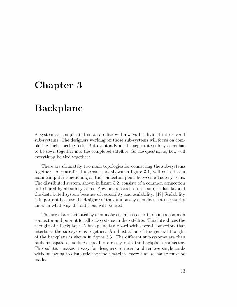
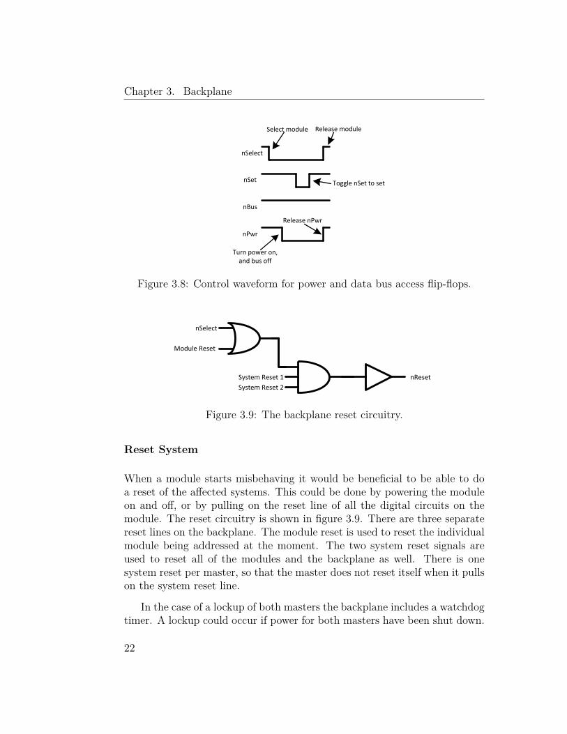
The data bus access and power switch is simply controlled by enable pins.These two pins could have been controlled directly from the master modules,but because of the pin count a better solution had to be found. A D-typeflip-flop is used for each signal to store the state, as shown in figure 3.7. Thecontrol bus for these flip-flops consists of a bus enable, power enable andclock signal. These signals are used together with the select signal to controlthe state of the flip-flop outputs. Figure 3.8 shows the correct waveforms forsetting the states.
21
Chapter 3. Backplane
nSelect
nSet
nBus
nPwr
Select module
Turn power on,and bus off
Toggle nSet to set
Release module
Release nPwr
Figure 3.8: Control waveform for power and data bus access flip-flops.
nSelect
Module Reset
System Reset 1
System Reset 2
nReset
Figure 3.9: The backplane reset circuitry.
Reset System
When a module starts misbehaving it would be beneficial to be able to doa reset of the affected systems. This could be done by powering the moduleon and off, or by pulling on the reset line of all the digital circuits on themodule. The reset circuitry is shown in figure 3.9. There are three separatereset lines on the backplane. The module reset is used to reset the individualmodule being addressed at the moment. The two system reset signals areused to reset all of the modules and the backplane as well. There is onesystem reset per master, so that the master does not reset itself when it pullson the system reset line.
In the case of a lockup of both masters the backplane includes a watchdogtimer. A lockup could occur if power for both masters have been shut down.
22

3.1. Design
nSelect
Pwr-state
En
Prog1
Prog2
Prog3
Prog4
Module prog1
Module prog2
Module prog3
Module prog 4
From masters
Figure 3.10: The backplane reprogramming circuitry.
Then there won’t be any controlling modules on the backplane, and thepower can’t be turned back on. The watchdog timer will then trigger andreset the power and bus flip-flops and reset the entire system. To preventthe watchdog timer from triggering one of the masters must toggle the firstaddressing pin.
Reprogramming Modules
In a harsh radiation such as space, memory cells will suffer from degradationand bit flips. If a firmware flash on an MCU is affected it could possiblyrender the device useless. The only way to recover the device would then beto reprogram the device. Most devices uses an interface, e.g. JTAG, ISP,TPI etc., with 4 lines or less to program the device. Therefore four signalsare routed from the masters to each module slot as a programming port. Theprogramming port is as default disconnected, and is connected whenever amodule is selected. The circuitry for handling this is shown in figure 3.10.
There doesn’t have to be made any decisions regarding the actual pro-gramming protocols to be used. It will just be a matter of implementing thevarious necessary protocols on the master modules later. Then the masterwill know which protocol to use depending on which address is going to bereprogrammed.
23

Chapter 3. Backplane
Figure 3.11: The module to backplane connector.
3.1.4 Mechanical Considerations
The satellite needs to be a mechanically reliable system. During launchthe satellite must endure immense accelerations and vibrations. This meansthat there are special concerns to be handled regarding the connectors usedfor each of the modules, and also for how the backplane itself is securedin the satellite. It is even important to concider component packaging andplacement to build a mechanical stable system.
The connector for the modules should be capable of providing the modulewith mechanical support in the satellite. It will act as an anchor point,and support the module together with the satellite’s frame. The selectedconnector is a regular 2.54mm pitch two row connector, as shown in figure3.11. It should provide sufficient support and be mechanical robust.
The circuit board of the backplane itself is shaped to be able to secure tothe frame of the satellite. It is meant to fit into slots in the frame, and besecured by screws in the corner. The shape of the circuit board can be seenin figure 3.14.
24

3.2. Prototyping
3.1.5 System Overview
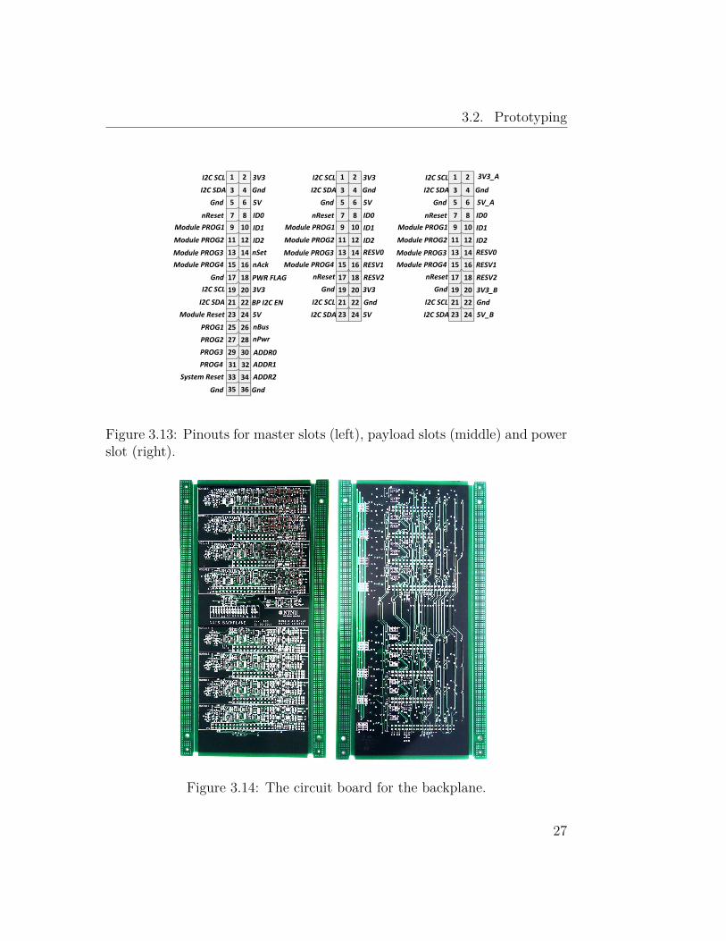
An overall overview of the backplane system is shown in figure 3.12. Itconsists of six 12x2 pin 2.54mm connectors, for regular payload and power,and two 18x2 pin 2.54mm connectors for the master modules. It is proposedthat the master modules are the radio module and the OBC. The mastershave the ability to control access to the common I2C bus, toggle power foreach module, reprogram modules and reset specific modules. The connectorpinouts for both the master modules, power module and payload modulesare shown in figure 3.13.
3.2 Prototyping
The proposed solution has been realized and tested. The schematics arepresented in appendix A. Figure 3.14 shows the PCB, both unassembled andassembled.
3.2.1 Testing
The basic functionality of the backplane has been tested by the steps shownin table 3.2. The first step was to do a visual inspection of the circuit boardto check that all ICs were mounted correctly, and that there were no shortcircuits before powering the board. Power was applied to the power slot ofthe backplane, and the power levels throughout the board were verified usinga multimeter. The redundancy of the power system was tested by removingpower to one of the power contacts from the power slot, and then measuringthat the power was still present. The current limiting circuits were also testedby short-circuiting the power terminals.
The digital systems were thoroughly tested in incremental steps. ProperI2C signalling, communication and full speed has been tested by checkingthat the I2C current monitor circuits could be read. Then, by hard-wiringaddresses for each slot, an acknowledge signal was verified when the correctaddress was applied. The remaining tests were performed by attaching anMCU to the control ports. Bus access, power and reset signals have been
25

Chapter 3. Backplane
Module 1Payload
Module 2Payload
Module 4Power
Module 5Master1
Module 6Payload
Module 7Payload
Module 8Master2
Module 3Payload
3v35v
a b a b
IdealDiodes
Curr.Limit
Curr.Limit
Curr.Meas.
Curr.Meas.
BP I2C
3v3
5v
Power
Power
5v
3v3
Power
5v
3v3
Power
5v
3v3
Power
5v
3v3
Power
5v
3v3
Power
5v
3v3
I2CRepeater
I2CRepeater
I2CRepeater
I2CRepeater
I2CRepeater
I2CRepeater
I2CRepeater
I2CRepeater
SDA SCL
I2C Bus
Control Bus:ADDR, Module Reset, System Reset, nSet,
nPwr, nBus, nAck, Pwr Flag, BP I2C EN
Figure 3.12: An overview of the backplane, excluding control logic.
26
3.2. Prototyping
1 2
3 4
5 6
7 8
9
11 12
13 14
15 16
17 18
19 20
21 22
23 24
25 26
27 28
29 30
31 32
33 34
35 36
10
I2C SCL
I2C SDA
I2C SCL
I2C SDA
Gnd
Gnd
Gnd
Gnd
Gnd
3V3
3V3
5V
5V
ADDR0
ADDR1
ADDR2
nBus
nPwr
BP I2C EN
PWR FLAG
nAck
nSet
ID0
ID1
ID2
nReset
Module PROG1
Module PROG2
Module PROG3
Module PROG4
PROG1
PROG2
PROG3
PROG4
System Reset
Module Reset
1 2
3 4
5 6
7 8
9
11 12
13 14
15 16
17 18
19 20
21 22
23 24
10
I2C SCL
I2C SDA
I2C SCL
I2C SDA
Gnd
Gnd
Gnd
3V3
3V3
5V
5V
Gnd
RESV2
RESV1
RESV0
ID0
ID1
ID2
nReset
Module PROG1
Module PROG2
Module PROG3
Module PROG4
nReset
1 2
3 4
5 6
7 8
9
11 12
13 14
15 16
17 18
19 20
21 22
23 24
10
I2C SCL
I2C SDA
I2C SCL
I2C SDA
Gnd
Gnd
Gnd
3V3_A
3V3_B
5V_A
5V_B
Gnd
RESV2
RESV1
RESV0
ID0
ID1
ID2
nReset
Module PROG1
Module PROG2
Module PROG3
Module PROG4
nReset
Figure 3.13: Pinouts for master slots (left), payload slots (middle) and powerslot (right).
Figure 3.14: The circuit board for the backplane.
27

Chapter 3. Backplane
Figure 3.15: The finished backplane with OBC module.
toggled using the control bus. The programming interface have been testedusing a JTAG interface connected to another MCU.
Table 3.2: Testing specification of the backplane.
Step Functionality Specification1 Visual inspection Check components and soldering2 Basic power Apply power to both3 Redundant power Remove power from one4 Over-Current protection Short-circuit power signals5 I2C signalling Pull and release I2C lines6 I2C communication Read current measurement ICs7 I2C speed Read at 400kHz8 Module addressing Addressed a slot9 Power and bus control Turn on/off controls10 Ack and power flag Address module and check flags11 Reset system System and module reset12 Programming bus Signal propagation to module13 Programming bus JTAG programming
28
3.2. Prototyping
3.2.2 Results
Overall, the backplane is functioning as expected. However, there have beena few problems regarding the pull-up resistors for the I2C bus and the firstaddress bit. The bus repeaters needed a lower resistance than the defaultvalue of 10k ohms on the common backplane side, to be able to release thebus after a zero was transmitted. This is probably due to the load all therepeaters puts on the common bus, and the resistor is not sufficient to pullthe line high again. The first address line also had troubles being pulled high.The watchdog timer required a larger current to pull the line high.
The maximum speed of the I2C bus exceeds the specified 400kHz, butcommunication speeds should still be limited to 400kHz for reliable commu-nication. The programming bus was tested at speeds up to 500kHz, but itcan probably work with higher speeds.
Power Consumption
The backplane’s power consumption was measured to be ∼20mA. The back-plane logics runs at 3.3V, and the total power consumption is thus 66mW.The power consumption will of course increase with control and I2C busactivity because of the pull-up resistors.
29

30

Chapter 4
On-Board Controller
The main tasks of the On-Board Controller are to keep track of the satel-lite’s health, help to increase it’s life span and provide support with storageand/or processing capabilities. It will serve as one of the two backplanemasters, and will use it’s heightened responsibility to monitor and act on allcommunication and behavior of the satellite.
Since the OBC will have a supervising responsibility, it is natural that itretains a log of events and house-keeping data. It could be interesting to beable to download this log, or at least a summary, and analyze the behaviorof the satellite. Especially getting detailed logs of error condition would behelpful.
It is also desirable that the OBC can be used as a helpful tool before flightas well. The OBC can perform debug tasks as monitoring the messages onthe data bus and power consumption, reprogram modules on request etc. Itwould therefore be advantageous to provide an option to interface the OBCto a computer.
4.1 Hardware Design
The hardware will mainly consist of the connector for the backplane, anMCU for processing and memory for different purposes. Because of space andpower restrictions, hardware redundancy will not be prioritized. Although,
31

Chapter 4. On-Board Controller
methods for increasing reliability are discussed and planned for. Methods forusing the OBC for manual backplane control are also implemented.
4.1.1 Microcontroller
There were several issues to think about before selecting an MCU. It had toprovide low-power modes or sleep modes for saving power, and also be ableto process a sufficient amount of data. Since the board were to contain alot of memory, it was also desirable to have integrated support for variousmemory busses. Another aspect was that the MCU should preferably be ofa familiar architecture for both the author and the succeeding developers.
The final choice was the AT32UC3A3256 MCU from Atmel. It runs onthe AVR32 core which is designed with power-saving in mind, and offers pro-cessing capabilities with up to 92 DMIPS. There is some DSP instructionsavailable, which could be useful for image processing or other sensory equip-ment. There is also internal support for many different memory types, andan ECC generator with support for both Hamming codes and Reed Solomoncodes.
4.1.2 Memory Hierarchy
The memory setup will be used for logging events in the satellite, temporaryprocessing storage, module firmwares and possible more. It must thereforecontain some different type of memory to accommodate all uses. It shouldalso be taken into consideration that some memory types are volatile againstradiation, and can suffer bit-flips. Also, all memories that are not radiationhardened are vulnerable against latch-up in the on-chip digital circuits, butthose will hopefully be handled by the power system of the backplane.
First of all an SRAM chip is needed to expand on the limited amount ofon-chip Random Access Memory (RAM) on the MCU. This type of memoryhas a low access time and will help speed up the calculations. Unfortunately,they are sensitive to radiation and bit-flips are a potential danger. [21] Aradiation hardened SRAM would have solved this, but as the availabilityof those are limited a regular variant is still used. The specific chip used
32
4.1. Hardware Design
is IS61WV102416BLL-10TLI, and expands the MCU RAM with 16Mbit ofstorage.
For a more long-term logging of data a non-volatile memory was needed.There is also a possibility of SEU for non-volatile memories, so the idea wasto store redundant information to be able to detect any anomalies. By usinga sophisticated ECC it is possible to use a relatively small amount of bits todetect a fair amount of bit errors, and even correct them. A NAND flash hasbeen used because it comes in relatively large sizes, and there won’t be anyconcerns for having too little space for adding redundancy. A 16Gbit flash,MT29F16G08DAAWP, gives the possibility of storing a lot of housekeepingdata and even images.
The firmware for the different modules in the satellite are most commonlystored in a on-chip flash on the separate MCUs. This flash is also volatileto radiation, and can be struck by a SEU that flips a bit. It will then benecessary to have something to compare the firmware with to detect theerror in the flash. When an error is detected the known correct firmwarecan be uploaded. A correct firmware version must then be available for theOBC. This is done by using an OTP memory which is known to be speciallytolerant against radiation. The OTP memory will contain the firmware andperhaps other default settings for all of the modules, and can be used tocompare and correct errors.
4.1.3 Backplane Connector
Since the OBC is a master, it will have a master connector following thepinout from figure 3.13. The I2C bus signals are connected to the Gen-eral Purpose Input/Output (GPIO) pins with integrated I2C support. Thismeans that the MCU can communicate over the I2C bus with much lessprocessing power. The control signals are connected to normal GPIO, andwill be configured to use open-drain signalling. This is done to assure thatif the two masters fight over control of the backplane (i.e. one master wantto transmit 0, and the other master tries to transmit 1) they won’t harm theoutput stage of the GPIO pin.
33

Chapter 4. On-Board Controller
AT32UC3A3256
SRAM16Mbit
NAND 16Gbit
OTP4Mbit
Data b
us
USB
Backplane Connector
RF Link
Ove
rride
Figure 4.1: A system overview of the OBC.
4.1.4 USB Interface
An USB interface would be a simple way to communicate with the satellite.It could be used to debug and configure the satellite, both in the developmentprocess and just before launch. Since the selected MCU has direct supportfor USB it was not necessary to add any new chips to the design. The MCUis programmed to enumerate on the computer as a standard COM-port andthe user can then decide to use a simple terminal or a specialized programto communicate with the satellite.
4.1.5 Manual Override
There are also possible to override the backplane control signals manually.By using some jumpers placed at the edge of the OBC most of the backplanecontrol signals can be operated to e.g. turn off power for a module, select amodule for programming and check the power state.
4.1.6 Hardware Overview
An overview of the hardware design for the OBC is shown in figure 4.1. TheAT32UC3A3 MCU is connected to the memory hierarchy with a common
34

4.2. Software Design
parallell bus. The backplane control signals are connected directly to generalpurpose input/output pins of the MCU, and some are also connected to themanual override headers. The USB connector is connected to the MCU aswell. The wireless module shown in the figure will be discussed in chapter 5.
4.2 Software Design
The OBC will need a complex piece of software to function as a master forthe satellite. It has been given many tasks, and all of them needs to behandled in an efficient and secure manner. Because of it’s heightened statusas a master on the backplane, it has a lot of responsibility to not abuse it’spower and perform potentially devastating mistakes. This has to be kept inmind when developing the software.
A lot of the development work for the OBC software still remains, butan overall idea for the various tasks and abilities of the software is outlined.Some aspects have been tested, and hardware specific drivers have been de-veloped and can be used in the future.
4.2.1 Drivers
The OBC contains 3 different types of memory devices which have been inter-faced to the same bus interface, but in a slightly different way. This requiressome configuration and setup in software in order to work as expected. TheSRAM and OTP memory uses a standard random access addressed interface,but the NAND flash uses a command interface to read and store pages ofdata. This requires a little framework in order to function.
The USB interface also needs some drivers to work. Actually it wouldtake several days, or even weeks, of work to get a usable USB stack upand running. Fortunately, Atmel provides a framework of drivers for mostmodules and the USB interface is one of them. This framework has beenused for both the USB interface and for the memories, with the exception ofthe NAND flash command interface.
Also, some drivers for the backplane has to be developed in order to con-trol all the functions properly. This includes turning the power and bus ac-
35

Chapter 4. On-Board Controller
cess on/off, resetting modules, interpreting bus activity and reprogrammingmodules. Even the reprogramming must be taken care of by implementing adriver for each of the supported protocols.
4.2.2 Housekeeping
Tasks as supervising the power consumption, bus activity, module healthetc. falls under housekeeping. This needs to be handled by the OBC byperiodically reading the current measurement circuits on the I2C bus, check-ing that communication is valid and sending a ping to each of the modules.Housekeeping data should also be stored to the NAND flash and could beused to create a summary for download to the ground station. Then theground station can request more detailed data of a duration in time thatseem interesting.
4.2.3 Operating System
Since the OBC will perform many separate tasks, it would be easier, moreefficient and more secure to use some sort of small operating system. Thereare many operating systems available to select from, and a suitable one shouldbe implemented at a later time.
4.2.4 Support Software
The support software will consist of a python script with a Graphical UserInterface (GUI). It will have the ability to connect to the OBC and monitorand control all of the OBC actions. E.g. power consumption, bus activity,module firmware etc. can be read and configured from the interface. Alldata can be sent and received using the USB interface with the COM-portemulation.
36

4.3. Prototyping
Figure 4.2: The circuit board for the OBC.
4.3 Prototyping
A prototype of the OBC has been developed and tested. The circuit diagramcan be found in appendix B. The circuit board is shown in figure 4.2, and anassembled version is shown in figure 4.3. Note that the OTP memory is notmounted since it has to be programmed using a special programmer beforemounting. The extra PCB on the top of the figure is the wireless internalcommunication module discussed in chapter 5.
4.3.1 Testing
The OBC module was tested by attaching it to the backplane through amaster slot before applying power to the backplane. Then using the manualoverride connectors in front on the OBC module, the address was set tothe OBC module itself. A JTAG programmer was attached to the JTAGconnector, and the chip ID of the MCU was read. To be able to fully debugthe rest of the system a firmware emulating a COM port through the USBinterface was programmed onto the MCU
A simple command interface using single letters, controlled which testthe MCU was going to run, and the result of the test was printed back on
37
Chapter 4. On-Board Controller
Figure 4.3: The finished OBC.
the terminal. A full write/read-test of the SRAM was performed, as well asa simple read test on the NAND flash. The OTP memory has unfortunatelynot been fully tested since the programming socket was not available.
The backplane was also controlled by the OBC to check that all theconnector pins were correctly placed. The I2C bus was used to read currentmeasurements from the backplane, and a simple JTAG programming driverwas written to read the ID from modules.
4.3.2 Results
All functionality of the OBC has proven to work. The memory ICs are ableto share a common bus, and operate at the timing specifications given in thedatasheet. This means that the PCB routing is not a limiting factor for thethroughput.
38
4.3. Prototyping
Power Consumption
The power consumption of the OBC module will rely heavily on the firmwarefor the MCU. In the worst case scenario with USB connected using no sleepmodes, not shutting of clock domains in the MCU or other power optimiza-tions the power consumption was ∼45mA, or ∼150mW. When putting theOBC into static sleep mode, which means all clocks are stopped, the powerconsumption fell to ∼4.5mA, or ∼15mW. The datasheet for the SRAM chipreports a nominal consumption of 4mA in retention mode, so below 0.5mAis used for the NAND flash.
It is much potential for saving power by carefully using sleep modes asmuch as possible. Even when the MCU can’t sleep it can save a lot of powerby using a low operating frequency when little processing power is required.A high frequency should be used when processor intensive tasks should bedone, so that the MCU can go back to sleep as soon as possible.
39

40
Chapter 5
Internal WirelessCommunication
There are certain disadvantages by using a standard electrically wired databus for communication between the modules. A short circuit is the firstproblem, which would cripple the whole bus. The only way to protect againstthis would be to have an extra data bus for redundancy. Another problemwould be if a module starts flooding the bus with garbage data.
One solution for all of this is to use a wireless data bus instead. Thereare many different wireless communication ICs available, and many are opti-mized for low-power and low-size applications. They also give the option tochange the communication frequency, which would fix the problem of a mod-ule flooding the data bus. A wireless bus is also more flexible since it doesn’trequire any concern for how to connect the different modules together.
Some of the modules in the student satellite will be equipped with awireless internal communication module, as described in this chapter. Thegoal is to test if a wireless internal data bus is a viable solution, and if it couldreplace the wired bus in the future. It should be as invisible as possible forthe module MCUs, i.e. provide a seamless wireless link between the modules.Therefore the wireless module has to be smart and be able to transmit andreceive data without help from the module MCU.
41

Chapter 5. Internal Wireless Communication
nRF24LE1 FilterSPI
Prog
Figure 5.1: An overview of the wireless transceiver module.
5.1 Hardware Design
Since the wireless module should be able to process the wireless transmissionsitself, it should contain some sort of a processing unit. There are a numberof single-chip solutions with a wireless transceiver and a MCU on the samechip. One of these are the nRF24LE1 from Nordic Semiconductor. Thischip has been selected because it can transmit at a rate of up to 2Mbps, andcomes in a variety where the firmware for the MCU is stored in an on-chipOTP memory. This will help improve the radiation tolerance of the wirelessmodules. Figure 5.1 shows an overview of the wireless module hardware.
The wireless module contains two crystal oscillators connected to thenRF24LE1 chip. A 16MHz crystal is needed for the wireless transceiver andas a MCU clock, and a 32.768kHz crystal will be used by the chip to synchro-nize timings of the wireless protocols. By having a reliable synchronizationit is possible to sleep between transceiving in order to save a substantialamount of power.
A chip antenna has been used instead of a trace antenna to eliminatethe need to experiment on the optimal length and geometry of the trace.In addition, the chip antenna takes up a much smaller area than the traceantenna would have. A matching network of inductive coils and capacitorsare still needed in order to match the output stage of the wireless transceiverto the chip antenna.
A SPI interface will be used between the module MCU and the wirelessmodule. The SPI interface will provide a larger throughput than the I2C
42

5.2. Firmware Design
bus, and is necessary in order to take full advantage of the 2Mbps transferrate of the transceiver. Some extra connectors for reset and programminglines are added as well. These will be helpful during the development stage.
5.2 Firmware Design
Some firmware work is needed on the wireless module too. First of all adecent protocol must be found that will accommodate the various demandson throughput, latency and power consumption. A complicating piece of thepuzzle is that the wireless network should be self-reliant and not dependingon any form of master node. Some suggestive ideas for the protocol is givenin section 5.2.1.
The firmware must also keep track of incoming and outgoing data, andwhere they come from and where they should be sent. Because of the limitedamount of memory in the rf transceiver IC, the buffer will be too small tohold a signficant amount of packages. Therefore it will be easiest to limitthe buffer to only be able to hold one incoming and one outgoing package atany given time.
The actual wireless packages from nRF24LE1 are limited to only 32 bytesper wireless transmission. If any more data is needed it must be split intoseveral transmissions. The protocol will be able to handle the transmissionof the entire buffer automatically, but if even larger amount of data needsto be transmitted, such as an image, it must be handled by the transmittingand receiving module MCUs.
5.2.1 Protocol
Addressed Transmission
The nRF24LE1 has the possibility to filter and buffer wireless packages basedon a separate address. If wireless module A is the receiver, it can configure sixindividual addresses used for six independent links. Then wireless moduleB has been given one of those six addresses to use when transmitting towireless module A. When wireless module B transmits a package with this
43

Chapter 5. Internal Wireless Communication
address, only wireless module A will receive this package, and will know thatthe message came from wireless module B because of the address that wasused. Table 5.1 shows an example address table for transmission between 3wireless modules.
Table 5.1: Example address table for wireless transmission.
Transmitter Receiver AddressModule A Module B 0Module A Module C 1Module B Module A 2Module B Module C 3Module C Module A 4Module C Module B 5
The disadvantage with this approach is that all modules must constantlybe in receive mode to check for messages. This will lead to a high powerconsumption. In addition, if two wireless modules start transmitting at thesame time both messages will be corrupted.
Separate Channels
A slightly different approach is to use a separate channel for each, instead ofthe addresses. This will eliminate the danger of collisions, but will still leadto a high power consumption since the modules have to listen all the time.Therefore it could be beneficial to combine the use of addresses and channels.By assigning a separate channel for all communications going to module A, B,C etc. and making the transmitter listen for an invitation before transmittingit is possible to put the devices into sleep mode occasionally. Table 5.2 showsa step by step instruction of how a transmission would occur.
44
5.2. Firmware Design
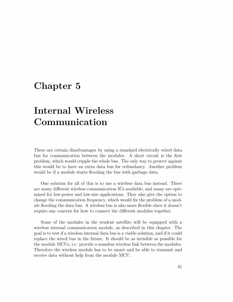
Table 5.2: A transmission from Module A to Module B.
Step Module A action Module B action1 Change to B channel Sleeping2 Waiting for invitation Invite C to start transmission3 Waiting for invitation Receiving4 Waiting for invitation Invite A to start transmission5 Transmit data Receiving6 Receive ack Send ack
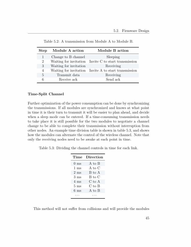
Time-Split Channel
Further optimization of the power consumption can be done by synchronizingthe transmissions. If all modules are synchronized and knows at what pointin time it is their turn to transmit it will be easier to plan ahead, and decidewhen a sleep mode can be entered. If a time-consuming transmission needsto take place it is still possible for the two modules to negotiate a channelchange to be able to complete their transmission without interruption fromother nodes. An example time division table is shown in table 5.3, and showshow the modules can alternate the control of the wireless channel. Note thatonly the receiving nodes need to be awake at each point in time.
Table 5.3: Dividing the channel controls in time for each link.
Time Direction0 ms A to B1 ms A to C2 ms B to A3 ms B to C4 ms C to A5 ms C to B6 ms A to B· · · · · ·
This method will not suffer from collisions and will provide the modules
45
Chapter 5. Internal Wireless Communication
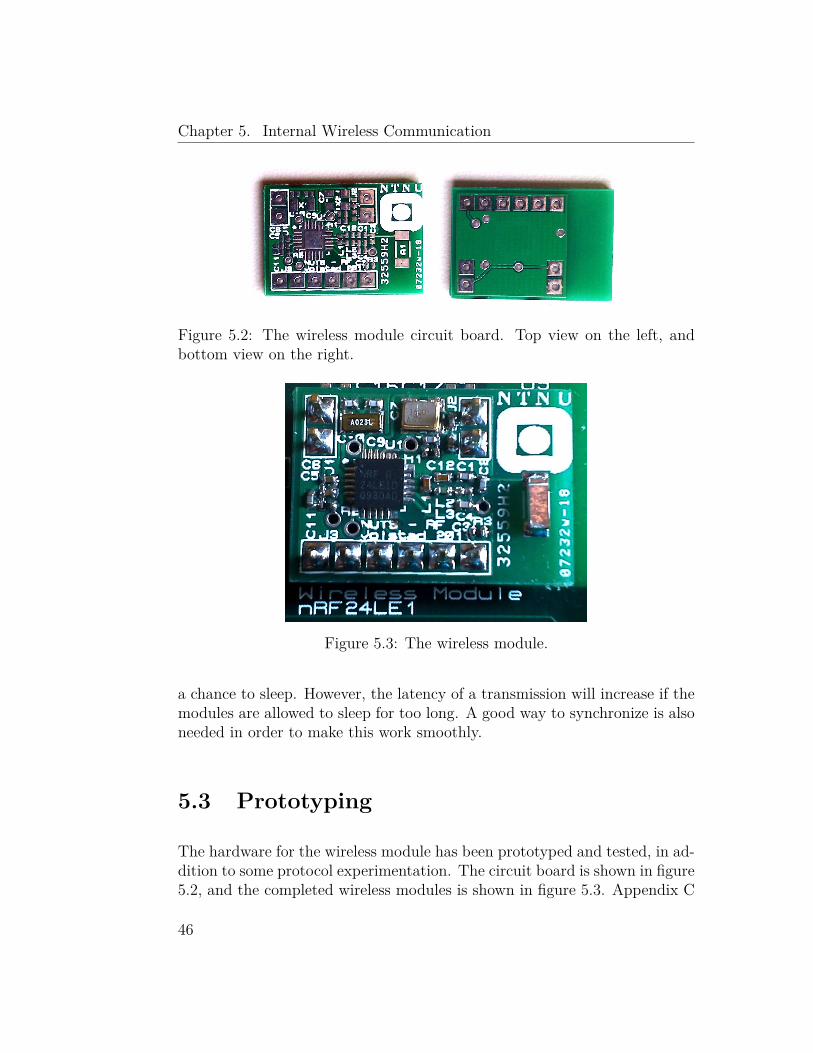
Figure 5.2: The wireless module circuit board. Top view on the left, andbottom view on the right.
Figure 5.3: The wireless module.
a chance to sleep. However, the latency of a transmission will increase if themodules are allowed to sleep for too long. A good way to synchronize is alsoneeded in order to make this work smoothly.
5.3 Prototyping
The hardware for the wireless module has been prototyped and tested, in ad-dition to some protocol experimentation. The circuit board is shown in figure5.2, and the completed wireless modules is shown in figure 5.3. Appendix C
46

5.3. Prototyping
shows the hardware schematics.
5.3.1 Testing
The wireless module was tested by programming it to constantly incrementa variable, and transmit it to a receiving development board with a display.The counter was displayed on the display. Some testing has also been doneon various ways to implement a communication protocol for the satellite.
5.3.2 Results
The wireless module is working as expected. Messages can be transmittedand received from the chip antenna. However, there is still some work leftto do to find a suitable protocol for communicating efficiently between all ofthe modules. It could be easier to find a suitable protocol when the completeusage of the wireless link has been decided.
Power Consumption
The power consumption of the wireless module is ∼20mA during constantreceive mode, and similar results for constant transmit mode. This is toomuch since there has to be one wireless module per backplane slot for acomplete communication system. However, experimentation with differentprotocols has shown that the power consumption can probably reach as lowas 2mA for each wireless module.
47

48

Chapter 6
Discussion
The satellite is suppose to be a self-reliant system. This means that it shouldbe able to automatically handle any error conditions that might occur duringit’s lifespan. It is unfortunately impossible to predict every single problemthat might occur. And not all of the ones that can be predicted will bepossible to account for completely. A solution using redundant componentswill consume a lot of space and extra power, and the complexity of con-necting these systems could lead to a more fragile system. Since NUTS willfollow the CubeSat specification it has a heavily limited amount of space andweight. Because of this, the solutions presented in this thesis has emphasizedsimplicity over a fully redundant system.
The amount of space available for each module is quite limited. Bydoing a simple design for the backplane it was possible to put all the necessarycontrol logic on it. This will ease the process for module designers, and makethe backplane more reliable since all control logic is the same. One simplemistake that could have been done is to use a different logic family for thecontrol logic. The logic families have been specially selected to account forvoltage range, speed, partial power down and other aspects.
The backplane solution takes care of the most important design aspects,which has been to not allow a single fault to take down the whole satellite.This has been done by being able to isolate modules from the rest of thesystem, and power down modules drawing too much current. There is evena redundant set of regulated power lines in case one regulator fails.
49
Chapter 6. Discussion
Space radiation will eventually incapacitate the satellite due to increas-ing TID, and it is difficult to slow down the process. The satellite has mostlybeen protected from SEU to stop a sudden radiation burst from causing toomuch damage. The over-current protection will hopefully act quick enoughto be able to stop a latch-up condition from damaging the die. And if thelatch-up does not draw enough power to trigger the over-current protection,the OBC will notice the anomaly and do a power toggling. Latch-up can beeliminated by building the logic gates using separate transistors, but it wouldconsume way too much area. SEU affecting memory cells will be detectedby the ECC. This will protect against a lot of possible hazards.
The OBC will have the main responsibility as a master module on thebackplane. It will keep polling the rest of the modules to make sure thesystem’s health is good. In addition, a log of events and statuses will bekept in a NAND flash. The NAND flash is not concidered to be a veryreliable memory, not even on the ground. Therefore much redundancy hasbeen planned for the flash memory. By using ECC and storing data twice,data should be kept intact even if some bits are flipped by SEU. There is stillthe possibility of the NAND flash logic failing totally, but that risk is alwayspresent, no matter what memory type is used.
The backplane master responsibility is shared with the radio module,which can take control when the ground station sends a specific command.If the OBC suddenly starts misbehaving, the radio module can take over andtry to restore the OBC. The radio can even hold a copy of the OBC firmwarein order to be able to reprogram it. If the OBC can’t be recovered, the radiomodule can shut off power to the OBC and continue acting as a master.
Power consumption for the backplane seems to be well below 100mW.From rough power calculations of the solar panel efficiency, the total powerbudget is about 4W. A consumption of 100mW is therefore a small piece ofthe total budget. For the OBC the power consumption will be dependent onthe programming of the MCU, but it is probable that it’s power consumptioncan end at 100mW also. The total power consumption would then be about5% of the total power budget, which should not be too demanding.
Intra-satellite wireless communication will be an interesting addi-tion to the regular wired bus. Since the total speed of the I2C bus has beenlimited to 400kb/s, the 2Mbit/s wireless link can be used to speed up trans-missions of larger data sets. It could even prove to be more power efficient to
50

use this high speed wireless link over the wired I2C bus. Since the I2C bussignals will have to propagate to several separate sub-domains with separatepull-ups. And transmissions will require longer time to complete on the I2Cbus, so power consumption could add up to be higher when using the wiredbus. In addition, the point to point transmission using the wireless bus willnot stop any other modules from communicating.
51

52
Chapter 7
Concluding Remarks
The overall system solution presented in this thesis seems to be a viabledesign for a reliable satellite. Although, radiation testing has not been donebecause of lack of equipment, the functionality of isolating separate modulesand others have been verified. The design has emphasized simplicity over acomplex redundant system, as this has several benefits such as lower area andpower consumption, and since simple systems generally are more reliable.
Low power consumption has been a constant criteria for the backplaneOBC and wireless communication module. With the OBC and backplaneconsuming 5% of the total power budget, there will be plenty of power leftfor other modules to perform their tasks. The wireless communication couldeven prove to improve on the overall power budget since transmissions canbe done quicker, and devices can go into sleep modes faster.
The abrasions from radiation can only be countered by shielding or us-ing different manufacturing processes for the ICs. These ICs are hard tofind, and it is almost impossible to shield from the most energetic particles.Therefore eventual failure will occur. However, the most drastic effects ofspace radiation, such as latch-up and bit-flips, have been taken into accountand compensated for in the design. The total lifespan of the satellite will beincreased by the proposed solutions.
53

54

Chapter 8
Future Work
8.1 Wireless link
The exact usage of the wireless link must be assessed, and a suitable protocolmust be implemented. For now the wireless link is considered an experimentto look at the viability of an internal wireless bus for communications.
8.2 OBC Completion
There are still a lot of work remaining on the OBC module. The behavior ofthe firmware has only been outlined, and some drivers developed. Still theimplementation needs to be done and thoroughly tested. A file system shouldbe implemented on the NAND flash device for logging, and other usage. TheOTP memory also need some sort of structure.
8.3 Radiation Detector
There should also be done some research on adding a radiation detectorcircuit to the system. A photodiode can be used to detect charge injectionsdue to ionizing radiation. This actually works much the same way as the
55

Chapter 8. Future Work
reason for latch-up and bit-flips. A charge is injected on the die, and flowsas a current through the sensor. This minute current can be amplified andmeasured to attain an approximation of the amount of radiation.
The measurements can be logged and downloaded to the ground station.It could be interesting to see the changes in radiation at various locationsin the Van Allen belt, and also compared to the solar cycle. In addition,the measurements could be used by the OBC to determine if certain fragilesystems should be shut down during intense radiation showers.
56

Bibliography
[1] “Space radiation effects on electronic components in low-earth orbit,”tech. rep., NASA, April 1996. Practice No. PD-ED-1258.
[2] R. A. Mewaldt, “Cosmic rays,” 1996.
[3] “Van allen radiation belt.” http://www.britannica.com/EBchecked/topic/622563/Van-Allen-radiation-belt.
[4] J. P. Uyemura, Introduction to VLSI Circuits and Systems. John Wiley& Sons, Inc., 2002.
[5] “Single event latchup.” http://www.aero.org/capabilities/seet/SElatchup.html.
[6] S. Kayali, “Space radiation effects on microelectronics.” http://parts.jpl.nasa.gov/docs/Radcrs_Final.pdf.
[7] “Understanding latch-up in advanced cmos logic.” http://www.fairchildsemi.com/an/AN/AN-600.pdf, April 1999. AN-600.
[8] S. Chen, “What types of ecc should be used on flash memory?,” tech.rep., Spansion, November 2007.
[9] N. Marquardt, “Introduction to the principles of vacuumphysics.” http://www.cientificosaficionados.com/libros/CERN/vacio1-CERN.pdf.
[10] D. Wright, “Space debris.” http://www.ucsusa.org/assets/documents/nwgs/wright-space-debris-physics-today.pdf, Octo-ber 2007.
57
Bibliography
[11] T. Miyahira and G. Swift, “Evaluation of radiation effectsin flash memories.” http://klabs.org/richcontent/MAPLDCon98/Papers/c4_miyahira.doc.
[12] A. S. Sedra and K. C. Smith,Microelectronic Circuits. Oxford UniversityPress, 2004.
[13] “Evaluating embedded non-volatile memory for 65nm and beyond.”http://www.sidense.com/images/stories/designcon_8_a_eval_embedded_nvm_65nm_and_beyond.pdf, 2008.
[14] H. S. R. S. V. L. G. L. Hans Reisinger, Martin Franosch and H. Wendt,“Patent no. us 6,215,140 b1 - electrically programmable non-volatilememory cell configuration,” tech. rep., Siemens Aktiengesellschaft, April2001.
[15] J. Benedetto and C. Hafer, “Ionizing radiation response of an amorphoussilicon based antifuse,” in Radiation Effects Data Workshop, 1997 IEEE,pp. 101 –104, jul 1997.
[16] “Logic guide.” http://focus.ti.com/lit/sg/sdyu001z/sdyu001z.pdf, 2009.
[17] “At32uc3a3 datasheet,” March 2010.
[18] “nrf24le1 - ultra-low power wireless system on-chip solution,” August2010.
[19] I. Helland, “Systems platform for nano and pico satellites,” January2009.
[20] “Um10204 - i2c-bus specification and user manual - rev.03,” tech. rep.,NXP, June 2007.
[21] G. S. L.Z. Scheick and S. Guertin, “Seu evaluation of sram memories forspace applications,” 2001.
58

Appendix A
Backplane
The source drawings for the hardware of the design is located in this section.
59

Appendix A. Backplane
5 5
4 4
3 3
2 2
1 1
DD
CC
BB
AA
Initial Pre-Release Version
NUTS Backplane
PA00
Board Function
Page
Front Page
1 2
Revision History
Comment
Revision
Module Connectors
Power Module 1 & 2
3
Power Module 3 & 4
4 5Power Module 5 & 6
6Power Module 7 & 8
7Bus Logic Module 1 & 2
8 9 10
Bus Logic Module 3 & 4
Bus Logic Module 5 & 6
Bus Logic Module 7 & 8
PA01
11
Backplane Logic & Pull-ups
Fixed errors from initial review
A00
First Release Version
Size
Des
igne
d:
Rev
isio
n
Shee
t of
Appr
oved
:
Shee
t Cre
ated
Dat
eSh
eet M
odifi
ed D
ate
Doc
umen
t num
ber
Sch
emat
ic T
itle
Des
ign
Cre
ated
Dat
e:
BOM
Doc
No:
Pag
e Ti
tle
A00
<Doc
>Su
nday
, Mar
ch 2
0, 2
011
111
A3<O
rgAd
dr1>
<Org
Addr
2>
NU
TS B
ackp
lane
<Cag
e C
ode>
Frid
ay, F
ebru
ary
18, 2
011
Frid
ay, F
ebru
ary
18, 2
011
TOP
/
Fron
t Pag
e
Figure A.1: Backplane schematic, page 1.
60
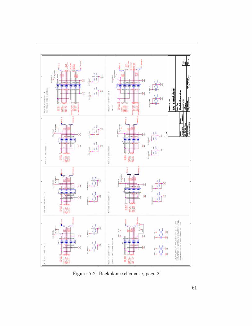
5 5
4 4
3 3
2 2
1 1
DD
CC
BB
AA
Module Connector 1
Module Connector 2
Module Connector 3
Module Connector 4
Module Connector 5
Module Connector 6
Module Connector 7
Module Connector 8
On Board Data Handling
RADIO
Electrical Power System
The EPS supplies the 3V3_A, 3V3_B, 5V_A and
5V_B rails. The module 5 power distribution
circuit is used to provide protection to the
backplane. Module 5 power cannot be turned
off.
ID10
ID11
ID12
RES
V0R
ESV1
RES
V2
ID20
ID21
ID22
RES
V0R
ESV1
RES
V2
ID30
ID31
ID32
RES
V0R
ESV1
RES
V2
ID50
ID51
ID52
RES
V0R
ESV1
RES
V2
ID60
ID61
ID62
RES
V0R
ESV1
RES
V2
ID70
ID71
ID72
RES
V0R
ESV1
RES
V2
ID40
ID41
ID42
ADD
R0
ADD
R1
ADD
R2
ADD
R0
ADD
R1
ADD
R2
ID80
ID81
ID82
3V3_
MO
DU
LE1
5V_M
OD
ULE
1
GN
DG
ND
3V3_
MO
DU
LE2
5V_M
OD
ULE
2
GN
DG
ND
3V3_
MO
DU
LE3
5V_M
OD
ULE
3
GN
DG
ND
3V3_
A5V
_A
GN
DG
ND
3V3_
MO
DU
LE6
5V_M
OD
ULE
6
GN
DG
ND
3V3_
MO
DU
LE7
5V_M
OD
ULE
7
GN
DG
ND
GN
D
3V3_
MO
DU
LE4
5V_M
OD
ULE
4
GN
D
GN
DG
ND
3V3_
MO
DU
LE8
5V_M
OD
ULE
8
3V3_
B5V
_B
GN
DG
ND
GN
DG
ND
3V3_
A3V
3_B
5V_A
5V_B
GN
D
3V3_
MO
DU
LE3
5V_M
OD
ULE
3
GN
DG
ND
GN
D
3V3_
MO
DU
LE4
5V_M
OD
ULE
4
GN
D
3V3_
MO
DU
LE1
GN
D
5V_M
OD
ULE
1
GN
DG
ND
3V3_
MO
DU
LE2
5V_M
OD
ULE
2
GN
DG
ND
3V3_
MO
DU
LE6
5V_M
OD
ULE
6
GN
DG
ND
GN
DG
ND
3V3_
MO
DU
LE7
5V_M
OD
ULE
73V
3_M
OD
ULE
85V
_MO
DU
LE8
RES
ET#1
I2C
_SC
L1I2
C_S
DA1
ID1[
2..0
]
RES
V[2.
.0]
RES
ET#2
I2C
_SC
L2I2
C_S
DA2
ID2[
2..0
]
RES
V[2.
.0]
RES
ET#3
I2C
_SC
L3I2
C_S
DA3
ID3[
2..0
]
RES
V[2.
.0]
RES
ET#5
I2C
_SC
L5I2
C_S
DA5
ID5[
2..0
]
RES
V[2.
.0]
RES
ET#6
I2C
_SC
L6I2
C_S
DA6
ID6[
2..0
]
RES
V[2.
.0]
RES
ET#7
I2C
_SC
L7I2
C_S
DA7
ID7[
2..0
]
RES
V[2.
.0]
ID4[
2..0
]
ADD
R[2
..0]
BUS_
EN#
PWR
_EN
#
SET#
ACK# AD
DR
[2..0
]
BUS_
EN#
PWR
_EN
#
SET#
ACK#
ID8[
2..0
]
RES
ET#8
PWR
_FLA
G
PWR
_FLA
G
RES
ET#4
SYST
EM_R
ESET
#1
MO
DU
LE_R
ESET
#
SYST
EM_R
ESET
#2
MO
DU
LE_R
ESET
#
BP_I
2C_E
N
BP_I
2C_E
N
DBG
_TC
K2D
BG_T
DI2
DBG
_TM
S2D
BG_T
DO
2
DBG
_TD
I1
DBG
_TM
S1D
BG_T
DO
1D
BG_T
CK1
DBG
_TC
K3D
BG_T
DI3
DBG
_TM
S3D
BG_T
DO
3D
BG_T
CK4
DBG
_TD
I4
DBG
_TM
S4D
BG_T
DO
4
DBG
_TC
KD
BG_T
DI
DBG
_TD
OD
BG_T
MS
DBG
_TC
K5D
BG_T
DI5
DBG
_TM
S5D
BG_T
DO
5
DBG
_TC
K6D
BG_T
DI6
DBG
_TM
S6D
BG_T
DO
6D
BG_T
CK7
DBG
_TD
I7
DBG
_TM
S7D
BG_T
DO
7
DBG
_TC
K8D
BG_T
DI8
DBG
_TD
O8
DBG
_TM
S8
DBG
_TC
KD
BG_T
DI
DBG
_TD
OD
BG_T
MS
I2C
_SC
L8I2
C_S
DA8
I2C
_SC
L4I2
C_S
DA4
Size
Des
igne
d:
Rev
isio
n
Shee
t of
Appr
oved
:
Shee
t Cre
ated
Dat
eSh
eet M
odifi
ed D
ate
Doc
umen
t num
ber
Sch
emat
ic T
itle
Des
ign
Cre
ated
Dat
e:
BOM
Doc
No:
Pag
e Ti
tle
A00
<Doc
>Su
nday
, Mar
ch 2
0, 2
011
211
A3<O
rgAd
dr1>
<Org
Addr
2>
NU
TS B
ackp
lane
<Cag
e C
ode>
Frid
ay, F
ebru
ary
18, 2
011
Frid
ay, F
ebru
ary
18, 2
011
TOP
/
Mod
ule
Con
nect
ors
C25
100N
P71
2 4 86 10
3 5 97
1213
1411 15
1617
1819
2021
2223
24
C9
100N
C3
100N
C29
100N
C17
100N
C19
100N
C5
100N
C28
100N
C30
100N
P21
2 4 86 10
3 5 97
1213
1411 15
1617
1819
2021
2223
24
C32
100N
C10
100N
C11
100N
C26
100N
C20
100N
C6
100N
P61
2 4 86 10
3 5 97
1213
1411 15
1617
1819
2021
2223
24
C23
100N
C12
100N
P81
2 4 86 10
3 5 97
1213
1411 15
1617
1819
2021
2223
24
C15
100N
P51
2 4 86 10
3 5 97
1213
1411 15
1617
1819
2021 23 25 27
22 24 26 28 3031
3229 33
3435
36
C21
100N
C14
100N
C18
100N
C31
100N
P11
2 4 86 10
3 5 97
1213
1411 15
1617
1819
2021
2223
24
C4
100N
P31
2 4 86 10
3 5 97
1213
1411 15
1617
1819
2021
2223
24
C27
100N
C2
100N
P41
2 4 86 10
3 5 97
1213
1411 15
1617
1819
2021 23 25 27
22 24 26 28 3031
3229 33
3435
36 C24
100N
C22
100N
C16
100N
C1
100N
C13
100N
C7
100N
C8
100N
Figure A.2: Backplane schematic, page 2.
61
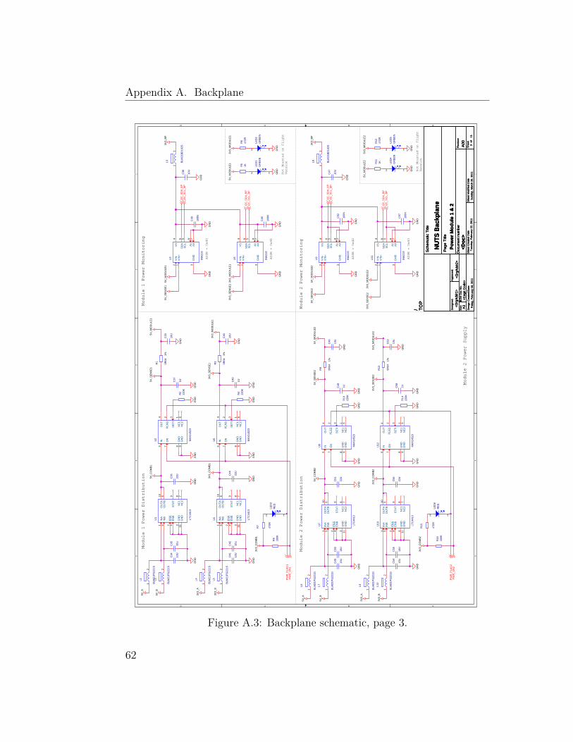
Appendix A. Backplane
5 5
4 4
3 3
2 2
1 1
DD
CC
BB
AA
Module 2 Power Supply
Not Mounted on Flight
Version
Not Mounted on Flight
Version
ADDR = 0x40
ADDR = 0x41
ADDR = 0x42
ADDR = 0x43
Module 1 Power Distribution
Module 1 Power Monitoring
Module 2 Power Monitoring
Module 2 Power Distribution
3V3_
A
3V3_
B
GN
DG
ND
5V_A
5V_B
GN
DG
ND
GN
D
GN
D
GN
D
GN
D
GN
D
GN
D
GN
D
GN
D
5V_M
OD
ULE
1
3V3_
MO
DU
LE1
3V3_
A
3V3_
B
GN
DG
ND
5V_A
5V_B
GN
DG
ND
GN
D
GN
D
GN
D
GN
D
GN
D
GN
D
5V_M
OD
ULE
2
3V3_
MO
DU
LE2
GN
D
GN
D
GN
D
3V3_
BP
3V3_
CO
MB1
3V3_
CO
MB1
5V_C
OM
B1
GN
DG
ND
5V_M
OD
ULE
23V
3_M
OD
ULE
2
GN
DG
ND
5V_M
OD
ULE
13V
3_M
OD
ULE
1
5V_C
OM
B2
3V3_
CO
MB2
3V3_
CO
MB2
GN
D
GN
D
GN
D
3V3_
BP
GN
D
GN
D
GN
D
GN
D
GN
D
GN
D
5V_M
OD
ULE
1
3V3_
MO
DU
LE1
5V_S
ENSE
1
3V3_
SEN
SE1
3V3_
SEN
SE1
5V_S
ENSE
1
5V_S
ENSE
25V
_SEN
SE2
5V_M
OD
ULE
2
3V3_
MO
DU
LE2
3V3_
SEN
SE2
3V3_
SEN
SE2
PWR
_ON
1PW
R_F
LAG
1
PWR
_FLA
G2
PWR
_ON
2
I2C
_SD
A_BP
I2C
_SC
L_BP
I2C
_SD
A_BP
I2C
_SC
L_BP
I2C
_SC
L_BP
I2C
_SD
A_BP
I2C
_SC
L_BP
I2C
_SD
A_BP
Size
Des
igne
d:
Rev
isio
n
Shee
t of
Appr
oved
:
Shee
t Cre
ated
Dat
eSh
eet M
odifi
ed D
ate
Doc
umen
t num
ber
Sch
emat
ic T
itle
Des
ign
Cre
ated
Dat
e:
BOM
Doc
No:
Pag
e Ti
tle
A00
<Doc
>Su
nday
, Mar
ch 2
0, 2
011
311
A3<O
rgAd
dr1>
<Org
Addr
2>
NU
TS B
ackp
lane
<Cag
e C
ode>
Tues
day,
Feb
ruar
y 22
, 201
1Fr
iday
, Feb
ruar
y 18
, 201
1
TOP
/
Pow
er M
odul
e 1
& 2
R15
470R
U12 MAX
1452
3
IN5
OU
T4
FLA
G2
ON
7
GN
D8
GN
D9
SE
TI3
NC
11
NC
26
C48
1U
L9
BLM
21PG
221S
12
L2
BLM
21PG
221S
12
LED
6R
ED
2 1
L4
BLM
21PG
221S
12
U8 MAX
1452
3
IN5
OU
T4
FLA
G2
ON
7
GN
D8
GN
D9
SE
TI3
NC
11
NC
26
L10
BLM
21PG
221S
12
R14
220K
U9 INA2
19
VIN
+1
VIN
-2
GN
D3
VS
4
SD
A6
SC
L5
A1
8
A0
7
R10
220K
C36
22U
C40
10U
C50
10U
L5
BLM
21PG
221S
12
C45
100N
C41
10U
C42
10U
C34
10U
R7
470R
C52
100N
C43
1U
C35
10U
U7 LTC
4413
INA
1O
UTA
10
INB
5O
UTB
6
GN
D3
GN
D11
EN
A2
EN
B4
STA
T9
NC
27
NC
18
C49
10U
C57
100N
LED
2G
REE
N
2 1
LED
3R
ED
2 1
R6
470R
LED
1G
REE
N
2 1
C54
10U
L8 BLM
21BD
102S
12
U2 MAX
1452
3
IN5
OU
T4
FLA
G2
ON
7
GN
D8
GN
D9
SE
TI3
NC
11
NC
26
U1 LTC
4413
INA
1O
UTA
10
INB
5O
UTB
6
GN
D3
GN
D11
EN
A2
EN
B4
STA
T9
NC
27
NC
18
L1
BLM
21PG
221S
12
C55
10U
R5
1K
R9
0R04
1%
C38
10U
U11 INA2
19
VIN
+1
VIN
-2
GN
D3
VS
4
SD
A6
SC
L5
A1
8
A0
7
R13
0R04
1%
L3 BLM
21BD
102S
12
LED
5G
REE
N
2 1
U5 MAX
1452
3
IN5
OU
T4
FLA
G2
ON
7
GN
D8
GN
D9
SE
TI3
NC
11
NC
26
R12
470R
R16
100K
LED
4G
REE
N
2 1
C53
10U
C56
22U
C46
10U
U10 LTC
4413
INA
1O
UTA
10
INB
5O
UTB
6
GN
D3
GN
D11
EN
A2
EN
B4
STA
T9
NC
27
NC
18
L6
BLM
21PG
221S
12
C33
10U
R11
1K
R4
220K
C39
100N
L7
BLM
21PG
221S
12
C37
1U
R1
0R04
1%
C51
22U
U6 INA2
19
VIN
+1
VIN
-2
GN
D3
VS
4
SD
A6
SC
L5
A1
8
A0
7
R8
100K
R2
220K
C58
1U
U4 LTC
4413
INA
1O
UTA
10
INB
5O
UTB
6
GN
D3
GN
D11
EN
A2
EN
B4
STA
T9
NC
27
NC
18
R3
0R04
1%
C47
10U
C44
22U
U3 INA2
19
VIN
+1
VIN
-2
GN
D3
VS
4
SD
A6
SC
L5
A1
8
A0
7
Figure A.3: Backplane schematic, page 3.
62
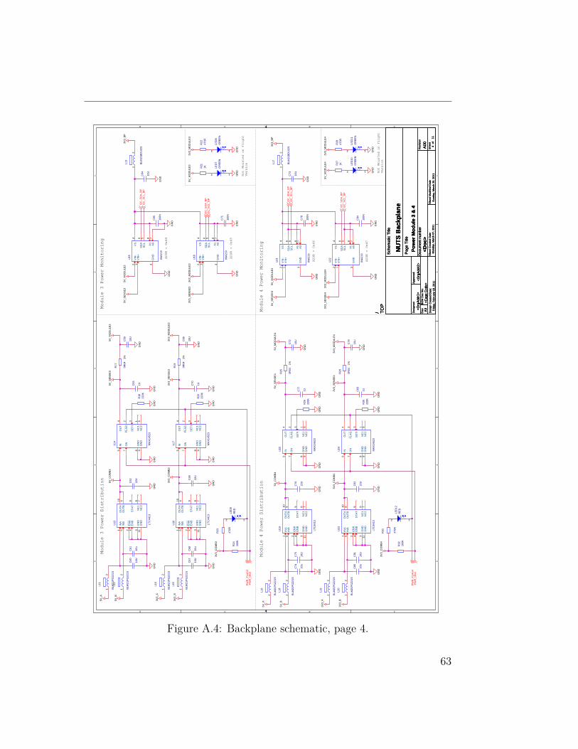
5 5
4 4
3 3
2 2
1 1
DD
CC
BB
AA
Not Mounted on Flight
Version
Not Mounted on Flight
Version
ADDR = 0x44
ADDR = 0x45
ADDR = 0x46
ADDR = 0x47
Module 3 Power Distribution
Module 3 Power Monitoring
Module 4 Power Monitoring
Module 4 Power Distribution
3V3_
A
3V3_
B
GN
DG
ND
5V_A
5V_B
GN
DG
ND
GN
D
GN
D
GN
D
GN
D
GN
D
GN
D
GN
D
GN
D
5V_M
OD
ULE
3
3V3_
MO
DU
LE3
3V3_
A
3V3_
B
GN
DG
ND
5V_A
5V_B
GN
DG
ND
GN
D
GN
D
GN
D
GN
D
GN
D
GN
D
5V_M
OD
ULE
4
3V3_
MO
DU
LE4
GN
D
GN
D
GN
D
3V3_
BP
3V3_
CO
MB3
3V3_
CO
MB3
5V_C
OM
B3
GN
DG
ND
5V_M
OD
ULE
43V
3_M
OD
ULE
4
GN
DG
ND
5V_M
OD
ULE
33V
3_M
OD
ULE
3
5V_C
OM
B4
3V3_
CO
MB4
3V3_
CO
MB4
GN
D
GN
D
GN
D
3V3_
BP
GN
D
GN
D
GN
D
GN
D
GN
D
GN
D
5V_S
ENSE
3
3V3_
SEN
SE3
5V_M
OD
ULE
35V
_SEN
SE3
3V3_
MO
DU
LE3
3V3_
SEN
SE3
5V_M
OD
ULE
4
3V3_
MO
DU
LE4
5V_S
ENSE
45V
_SEN
SE4
3V3_
SEN
SE4
3V3_
SEN
SE4
PWR
_ON
3PW
R_F
LAG
3
PWR
_FLA
G4
PWR
_ON
4
I2C
_SD
A_BP
I2C
_SC
L_BP
I2C
_SD
A_BP
I2C
_SC
L_BP
I2C
_SC
L_BP
I2C
_SD
A_BP
I2C
_SC
L_BP
I2C
_SD
A_BP
Size
Des
igne
d:
Rev
isio
n
Shee
t of
Appr
oved
:
Shee
t Cre
ated
Dat
eSh
eet M
odifi
ed D
ate
Doc
umen
t num
ber
Sch
emat
ic T
itle
Des
ign
Cre
ated
Dat
e:
BOM
Doc
No:
Pag
e Ti
tle
A00
<Doc
>Su
nday
, Mar
ch 2
0, 2
011
411
A3<O
rgAd
dr1>
<Org
Addr
2>
NU
TS B
ackp
lane
<Cag
e C
ode>
Mon
day,
Mar
ch 0
7, 2
011
Frid
ay, F
ebru
ary
18, 2
011
TOP
/
Pow
er M
odul
e 3
& 4
L11
BLM
21PG
221S
12
R30
220K
R27
1K
U21 INA2
19
VIN
+1
VIN
-2
GN
D3
VS
4
SD
A6
SC
L5
A1
8
A0
7
R25
0R04
1%
C60
10U
L15
BLM
21PG
221S
12
LED
9R
ED
2 1
C65
100N
R18
220K
R19
0R04
1%
C76
22U
C81
10U
LED
11G
REE
N
2 1
C67
10U
L14
BLM
21PG
221S
12
L17
BLM
21BD
102S
12
C80
10U
C59
10U
L12
BLM
21PG
221S
12
C63
1U
L19
BLM
21PG
221S
12
L13
BLM
21BD
102S
12
R23
470R
U24 MAX
1452
3
IN5
OU
T4
FLA
G2
ON
7
GN
D8
GN
D9
SE
TI3
NC
11
NC
26
C77
1U
C70
1U
L20
BLM
21PG
221S
12
C78
100N
U19 LTC
4413
INA
1O
UTA
10
INB
5O
UTB
6
GN
D3
GN
D11
EN
A2
EN
B4
STA
T9
NC
27
NC
18
R20
220K
U20 MAX
1452
3
IN5
OU
T4
FLA
G2
ON
7
GN
D8
GN
D9
SE
TI3
NC
11
NC
26
C79
10U
C61
10U
R22
470R
C75
10U
R32
100K
C83
1U
C74
10U
LED
12R
ED
2 1
C71
100N
C66
10U
R31
470RU23 LTC
4413
INA
1O
UTA
10
INB
5O
UTB
6
GN
D3
GN
D11
EN
A2
EN
B4
STA
T9
NC
27
NC
18
LED
7G
REE
N
2 1
LED
10G
REE
N
2 1
U13 LTC
4413
INA
1O
UTA
10
INB
5O
UTB
6
GN
D3
GN
D11
EN
A2
EN
B4
STA
T9
NC
27
NC
18
C73
10U
R29
0R04
1%
U14 MAX
1452
3
IN5
OU
T4
FLA
G2
ON
7
GN
D8
GN
D9
SE
TI3
NC
11
NC
26
U18 INA2
19
VIN
+1
VIN
-2
GN
D3
VS
4
SD
A6
SC
L5
A1
8
A0
7
C64
10U
L16
BLM
21PG
221S
12
R24
100K
U22 INA2
19
VIN
+1
VIN
-2
GN
D3
VS
4
SD
A6
SC
L5
A1
8
A0
7
U15 INA2
19
VIN
+1
VIN
-2
GN
D3
VS
4
SD
A6
SC
L5
A1
8
A0
7
R17
0R04
1%
C84
100N
L18
BLM
21PG
221S
12
R21
1K
C62
22U
C72
10U
C68
10U
U17 MAX
1452
3
IN5
OU
T4
FLA
G2
ON
7
GN
D8
GN
D9
SE
TI3
NC
11
NC
26
U16 LTC
4413
INA
1O
UTA
10
INB
5O
UTB
6
GN
D3
GN
D11
EN
A2
EN
B4
STA
T9
NC
27
NC
18
LED
8G
REE
N
2 1
R28
470R
C69
22U
C82
22U
R26
220K
Figure A.4: Backplane schematic, page 4.
63

Appendix A. Backplane
5 5
4 4
3 3
2 2
1 1
DD
CC
BB
AA
Not Mounted on Flight
Version
Not Mounted on Flight
Version
ADDR = 0x48
ADDR = 0x49
ADDR = 0x4a
ADDR = 0x4b
Backplane Power Distribution
Backplane Power Monitoring
Module 6 Power Distribution
Module 6 Power Monitoring
Since this module supplies the backplane power, it cannot be turned
off. (Turning off the backplane power will cause it to automatically
be turned on again anyway) Latch-up protection is still present.
3V3_
A
3V3_
B
GN
DG
ND
5V_A
5V_B
GN
DG
ND
GN
D
GN
D
GN
D
GN
D
GN
D
GN
D
GN
D
GN
D
5V_B
P
3V3_
BP
3V3_
A
3V3_
B
GN
DG
ND
5V_A
5V_B
GN
DG
ND
GN
D
GN
D
GN
D
GN
D
GN
D
GN
D
5V_M
OD
ULE
6
3V3_
MO
DU
LE6
GN
D
GN
D
GN
D
3V3_
BP
3V3_
CO
MB_
BP
5V_C
OM
B_BP
GN
DG
ND
5V_M
OD
ULE
63V
3_M
OD
ULE
6
GN
DG
ND
5V_B
P3V
3_BP
5V_C
OM
B6
3V3_
CO
MB6
3V3_
CO
MB6
GN
D
GN
D
GN
D
3V3_
BP
GN
D
GN
D
GN
D
GN
D
GN
D
GN
D
5V_S
ENSE
5
5V_S
ENSE
5
3V3_
SEN
SE5
3V3_
SEN
SE5
3V3_
BP
5V_B
P
5V_S
ENSE
6
3V3_
SEN
SE6
5V_M
OD
ULE
6
3V3_
MO
DU
LE6
5V_S
ENSE
6
3V3_
SEN
SE6
3V3_
CO
MB_
BP
PWR
_FLA
G6
PWR
_ON
6
I2C
_SD
A_BP
I2C
_SC
L_BP
I2C
_SD
A_BP
I2C
_SC
L_BP
I2C
_SC
L_BP
I2C
_SD
A_BP
I2C
_SD
A_BP
I2C
_SC
L_BP
Size
Des
igne
d:
Rev
isio
n
Shee
t of
Appr
oved
:
Shee
t Cre
ated
Dat
eSh
eet M
odifi
ed D
ate
Doc
umen
t num
ber
Sch
emat
ic T
itle
Des
ign
Cre
ated
Dat
e:
BOM
Doc
No:
Pag
e Ti
tle
A00
<Doc
>Su
nday
, Mar
ch 2
0, 2
011
511
A3<O
rgAd
dr1>
<Org
Addr
2>
NU
TS B
ackp
lane
<Cag
e C
ode>
Mon
day,
Mar
ch 0
7, 2
011
Frid
ay, F
ebru
ary
18, 2
011
TOP
<Sch
emat
ic P
ath>
Pow
er M
odul
e 3
& 4
L25
BLM
21PG
221S
12
U31 INA2
19
VIN
+1
VIN
-2
GN
D3
VS
4
SD
A6
SC
L5
A1
8
A0
7
U26 MAX
1452
3
IN5
OU
T4
FLA
G2
ON
7
GN
D8
GN
D9
SE
TI3
NC
11
NC
26
U30 INA2
19
VIN
+1
VIN
-2
GN
D3
VS
4
SD
A6
SC
L5
A1
8
A0
7
C99
10U
U34 INA2
19
VIN
+1
VIN
-2
GN
D3
VS
4
SD
A6
SC
L5
A1
8
A0
7
R41
220K
C85
10U
R42
1K
C86
10U
C91
100N
C87
10U
C10
9
100N
C10
7
10U
C89
22U
LED
16G
REE
N
2 1
C95
22U
L21
BLM
21PG
221S
12
R45
220K
U33 MAX
1452
3
IN5
OU
T4
FLA
G2
ON
7
GN
D8
GN
D9
SE
TI3
NC
11
NC
26
C10
8
22U
R39
220K
L30
BLM
21PG
221S
12
C10
0
10U
L22
BLM
21BD
102S
12
C10
4
1U
R36
0R04
1%
R44
0R04
1%
C90
1U
U29 MAX
1452
3
IN5
OU
T4
FLA
G2
ON
7
GN
D8
GN
D9
SE
TI3
NC
11
NC
26
R46
470R
LED
13
RED
21
R47
100K
R35
220K
C10
3
100N
LED
15G
REE
N
2 1
LED
17G
REE
N
2 1
C94
10U
U32 LTC
4413
INA
1O
UTA
10
INB
5O
UTB
6
GN
D3
GN
D11
EN
A2
EN
B4
STA
T9
NC
27
NC
18
C11
0
1U
R37
1K
C10
2
22U
L23
BLM
21PG
221S
12
U35 LTC
4413
INA
1O
UTA
10
INB
5O
UTB
6
GN
D3
GN
D11
EN
A2
EN
B4
STA
T9
NC
27
NC
18
C96
1U
L26
BLM
21PG
221S
12
U27 INA2
19
VIN
+1
VIN
-2
GN
D3
VS
4
SD
A6
SC
L5
A1
8
A0
7
C97
100N
U28 LTC
4413
INA
1O
UTA
10
INB
5O
UTB
6
GN
D3
GN
D11
EN
A2
EN
B4
STA
T9
NC
27
NC
18
R34
0R04
1%
LED
14G
REE
N
2 1
LED
18R
ED
2 1
L28
BLM
21PG
221S
12
R43
470R
C92
10U
R33
470R
C93
10U
C10
6
10U
C88
10U
C10
1
10U
U36 MAX
1452
3
IN5
OU
T4
FLA
G2
ON
7
GN
D8
GN
D9
SE
TI3
NC
11
NC
26
C10
5
10U
L29
BLM
21PG
221S
12
C98
10U
R38
470R
U25 LTC
4413
INA
1O
UTA
10
INB
5O
UTB
6
GN
D3
GN
D11
EN
A2
EN
B4
STA
T9
NC
27
NC
18
L27
BLM
21BD
102S
12
L24
BLM
21PG
221S
12
R40
0R04
1%
Figure A.5: Backplane schematic, page 5.
64

5 5
4 4
3 3
2 2
1 1
DD
CC
BB
AA
Module 7 Power Distribution
Not Mounted on Flight
Version
Not Mounted on Flight
Version
ADDR = 0x4d
ADDR = 0x4e
ADDR = 0x4f
ADDR = 0x4c
Module 7 Power Monitoring
Module 8 Power Monitoring
Module 8 Power Distribution
3V3_
A
3V3_
B
GN
DG
ND
5V_A
5V_B
GN
DG
ND
GN
D
GN
D
GN
D
GN
D
GN
D
GN
D
GN
D
GN
D
5V_M
OD
ULE
7
3V3_
MO
DU
LE7
3V3_
A
3V3_
B
GN
DG
ND
5V_A
5V_B
GN
DG
ND
GN
D
GN
D
GN
D GN
D
GN
D
GN
D
5V_M
OD
ULE
8
3V3_
MO
DU
LE8
GN
D
GN
D
GN
D
3V3_
BP
3V3_
CO
MB7
3V3_
CO
MB7
5V_C
OM
B7
GN
DG
ND
5V_M
OD
ULE
83V
3_M
OD
ULE
8
GN
DG
ND
5V_M
OD
ULE
73V
3_M
OD
ULE
7
5V_C
OM
B8
3V3_
CO
MB8
3V3_
CO
MB8
GN
D
GN
D
3V3_
BP
GN
D
GN
D
GN
D
GN
D
GN
D
5V_S
ENSE
7
GN
DG
ND
5V_M
OD
ULE
75V
_SEN
SE7
3V3_
MO
DU
LE7
3V3_
SEN
SE7
3V3_
SEN
SE7
5V_S
ENSE
8
3V3_
SEN
SE8
5V_M
OD
ULE
85V
_SEN
SE8 3V
3_M
OD
ULE
83V
3_SE
NSE
8
PWR
_ON
7PW
R_F
LAG
7
PWR
_FLA
G8
PWR
_ON
8
I2C
_SD
A_BP
I2C
_SC
L_BP
I2C
_SD
A_BP
I2C
_SC
L_BP
I2C
_SD
A_BP
I2C
_SC
L_BP
I2C
_SC
L_BP
I2C
_SD
A_BP
Size
Des
igne
d:
Rev
isio
n
Shee
t of
Appr
oved
:
Shee
t Cre
ated
Dat
eSh
eet M
odifi
ed D
ate
Doc
umen
t num
ber
Sch
emat
ic T
itle
Des
ign
Cre
ated
Dat
e:
BOM
Doc
No:
Pag
e Ti
tle
A00
<Doc
>Su
nday
, Mar
ch 2
0, 2
011
611
A3<O
rgAd
dr1>
<Org
Addr
2>
NU
TS B
ackp
lane
<Cag
e C
ode>
Mon
day,
Mar
ch 0
7, 2
011
Frid
ay, F
ebru
ary
18, 2
011
TOP
<Sch
emat
ic P
ath>
Pow
er M
odul
e 3
& 4
R57
220K
R58
1K
C12
0
10U
L38
BLM
21BD
102S
12
C11
1
10U
C11
3
10U
L35
BLM
21PG
221S
12
C12
2
1UR
5122
0K
R48
0R04
1%L3
3
BLM
21BD
102S
12
C12
7
10U
C13
6
100N
U43 INA2
19
VIN
+1
VIN
-2
GN
D3
VS
4
SD
A6
SC
L5
A1
8
A0
7
LED
22G
REE
N
2 1
C13
2
10U
C12
9
100N
R61
220K
R52
1K
R49
220K
C11
6
10U
U39 INA2
19
VIN
+1
VIN
-2
GN
D3
VS
4
SD
A6
SC
L5
A1
8
A0
7
LED
19G
REE
N
2 1
R50
0R04
1%
L36
BLM
21PG
221S
12
C13
1
10U
C12
5
10U
C11
9
10U
U44 LTC
4413
INA
1O
UTA
10
INB
5O
UTB
6
GN
D3
GN
D11
EN
A2
EN
B4
STA
T9
NC
27
NC
18
R53
470R
L39
BLM
21PG
221S
12
C13
3
10U
R55
100K
U37 LTC
4413
INA
1O
UTA
10
INB
5O
UTB
6
GN
D3
GN
D11
EN
A2
EN
B4
STA
T9
NC
27
NC
18
U38 MAX
1452
3
IN5
OU
T4
FLA
G2
ON
7
GN
D8
GN
D9
SE
TI3
NC
11
NC
26
C12
3
100N
R60
0R04
1%
C11
8
10U
L40
BLM
21PG
221S
12
C13
5
1U
U42 INA2
19
VIN
+1
VIN
-2
GN
D3
VS
4
SD
A6
SC
L5
A1
8
A0
7
C11
2
10U
U47 MAX
1452
3
IN5
OU
T4
FLA
G2
ON
7
GN
D8
GN
D9
SE
TI3
NC
11
NC
26
C12
8
22U
C13
4
22U
C12
1
22U
U45 MAX
1452
3
IN5
OU
T4
FLA
G2
ON
7
GN
D8
GN
D9
SE
TI3
NC
11
NC
26
C11
4
22U
C12
6
10U
C12
4
10U
LED
20G
REE
N
2 1
LED
24R
ED
2 1LE
D21
RED
2 1
R63
100K
R59
470R
U46 LTC
4413
INA
1O
UTA
10
INB
5O
UTB
6
GN
D3
GN
D11
EN
A2
EN
B4
STA
T9
NC
27
NC
18
R62
470R
C13
0
1U
R54
470R
L34
BLM
21PG
221S
12
U41 MAX
1452
3
IN5
OU
T4
FLA
G2
ON
7
GN
D8
GN
D9
SE
TI3
NC
11
NC
26
L32
BLM
21PG
221S
12
LED
23G
REE
N
2 1
R56
0R04
1%
L37
BLM
21PG
221S
12
U40 LTC
4413
INA
1O
UTA
10
INB
5O
UTB
6
GN
D3
GN
D11
EN
A2
EN
B4
STA
T9
NC
27
NC
18
C11
7
100N
C11
5
1U
L31
BLM
21PG
221S
12
U48 INA2
19
VIN
+1
VIN
-2
GN
D3
VS
4
SD
A6
SC
L5
A1
8
A0
7
Figure A.6: Backplane schematic, page 6.
65

Appendix A. Backplane
5 5
4 4
3 3
2 2
1 1
DD
CC
BB
AA
Decoupling
Decoupling
Module 1 Reset & Debug Signals
Module 1 Acknowledge & Power flag
Module 1 Address match, flip-flops & I2C repeater
Module 2 Address match, flip-flops & I2C repeater
Module 2 Acknowledge & Power flag
Module 2 Reset & Debug Signals
ID11
ADD
R0
ADD
R1
ADD
R2
PWR
_STA
TE#1
PWR
_STA
TE#1
SELE
CT#
1
SELE
CT#
1
PWR
_STA
TE#2
ID20
ID21
ID22
ADD
R2
ADD
R1
ADD
R0
SELE
CT#
2
PWR
_STA
TE#2
SELE
CT#
2
SELE
CT#
1
SELE
CT#
2
ID10
ID12
3V3_
BP
3V3_
MO
DU
LE1
GN
D
GN
D
3V3_
BP
3V3_
BP
GN
D
GN
D3V
3_BP
3V3_
BP
3V3_
BP
GN
D
GN
D3V
3_BP
3V3_
BP
3V3_
BP
GN
D
3V3_
MO
DU
LE2
3V3_
BP
GN
D
GN
D
GN
D
3V_I
2C
GN
D
3V_I
2C
GN
D
ID1[
2..0
]
ADD
R[2
..0]
DBG
_TC
KD
BG_T
DI
DBG
_TD
OD
BG_T
MS
DBG
_TC
K1D
BG_T
DI1
DBG
_TD
O1
DBG
_TM
S1
SET#
BUS_
EN#
PWR
_EN
#
BP_R
ESET
#
MO
DU
LE_R
ESET
#
RES
ET#1
PWR
_ON
1
SYST
EM_R
ESET
#1
SYST
EM_R
ESET
#2
ACK#
PWR
_FLA
G1
PWR
_FLA
G
SET#
PWR
_EN
#
BUS_
EN#
BP_R
ESET
#PW
R_O
N2
ID2[
2..0
]
ADD
R[2
..0]
DBG
_TC
KD
BG_T
DI
DBG
_TM
SD
BG_T
DO
DBG
_TD
I2D
BG_T
CK2
DBG
_TM
S2D
BG_T
DO
2
MO
DU
LE_R
ESET
#
RES
ET#2
SYST
EM_R
ESET
#1
SYST
EM_R
ESET
#2
ACK#
PWR
_FLA
G2
PWR
_FLA
G
I2C
_SC
LI2
C_S
DA
I2C
_SC
L1I2
C_S
DA1
I2C
_SC
L2I2
C_S
DA2
I2C
_SC
LI2
C_S
DA
Size
Des
igne
d:
Rev
isio
n
Shee
t of
Appr
oved
:
Shee
t Cre
ated
Dat
eSh
eet M
odifi
ed D
ate
Doc
umen
t num
ber
Sch
emat
ic T
itle
Des
ign
Cre
ated
Dat
e:
BOM
Doc
No:
Pag
e Ti
tle
A00
<Doc
>Su
nday
, Mar
ch 2
0, 2
011
711
A3<O
rgAd
dr1>
<Org
Addr
2>
NU
TS B
ackp
lane
<Cag
e C
ode>
Mon
day,
Mar
ch 0
7, 2
011
Frid
ay, F
ebru
ary
18, 2
011
TOP
/
Bus
Log
ic M
odul
e 1
& 2
C14
8
100N
U58
A
74LV
C1G
11
41 3 6
C21
3
100N
U55
B
34
U52
C
74LV
C2G
02G
ND
4
VC
C8
C15
4
100N
U61
C
89 10
U65
B
34
C14
3
100N
U68
A
74LV
C1G
11
41 3 6
C13
9
100N
R69
100K
U60
B
35 6
U52
B
35 6
U66
A74
LV40
66
1Y1
1Z2
1E13
2Y4
3Y8
4Y11
2Z3
3Z9
4Z10
2E5
3E6
4E12
U52
A
71 2
C14
4
100N
C14
0
100N
C21
2
100N
C13
8
100N
R68
10K
U55
A
16
U50
A
74LV
C74
A
1PR
E4
1CLK
3
1D2
1CLR
1
1Q5
1Q6
U49
A
31 2
C15
3
100N
R65
10K
U59
A
41 3 6
C15
0
100N
C15
2
100N
U61
A
31 2
U49
D
1112 13
C14
1
100N
C14
2
100N
U53 PC
A951
7Vcca1
SC
LA2
SD
AA
3
Gnd4
Vccb8
SC
LB7
SD
AB
6
EN
5
U63 PC
A951
7Vcca1
SC
LA2
SD
AA
3
Gnd4
Vccb8
SC
LB7
SD
AB
6
EN
5
U68
B
74LV
C1G
11
VC
C5
GN
D2
U59
B
74LV
C1G
332
GN
D2
VC
C5
U51
B
74LV
C1G
332
GN
D2
VC
C5
U50
B
74LV
C74
A
2PR
E10
2CLK
11
2D12
2CLR
13
2Q9
2Q8
U67
B
74LV
C1G
125
VC
C5
GN
D3
C13
7
100N
U49
B
64 5
U64
B
74LV
C1G
32G
ND
3
VC
C5
U50
C
74LV
C74
A
GN
D7
VC
C14
U56
B
74LV
4066VC
C14
GN
D7
C14
6
100N
C14
5
100N
U61
E
74LV
C86
A
VC
C14
GN
D7
U67
A
74LV
C1G
125
24
1
U54
B
74LV
C1G
32G
ND
3
VC
C5
C14
9
100N
U49
C
89 10
U65
A
16
U55
C
74LV
C2G
07
VC
C5
GN
D2
U62
A
74LV
C74
A
1PR
E4
1CLK
3
1D2
1CLR
1
1Q5
1Q6
U57
A
24
1
U54
A
41 2
R67
10K
U65
C
74LV
C2G
07
VC
C5
GN
D2
R66
100K
R64
10K
U57
B
74LV
C1G
125
VC
C5
GN
D3
U62
B
74LV
C74
A
2PR
E10
2CLK
11
2D12
2CLR
13
2Q9
2Q8
U66
B
74LV
4066VC
C14
GN
D7
U61
D
1112 13
U49
E
74LV
C86
A
VC
C14
GN
D7
U56
A74
LV40
66
1Y1
1Z2
1E13
2Y4
3Y8
4Y11
2Z3
3Z9
4Z10
2E5
3E6
4E12
C14
7
100N
U62
C
74LV
C74
A
GN
D7
VC
C14
U51
A
41 3 6
C15
1
100N
U64
A
41 2
U61
B
64 5
U58
B
74LV
C1G
11
VC
C5
GN
D2
U60
A
71 2
U60
C
74LV
C2G
02G
ND
4
VC
C8
Figure A.7: Backplane schematic, page 7.
66

5 5
4 4
3 3
2 2
1 1
DD
CC
BB
AA
Decoupling
Decoupling
Module 3 Reset & Debug Signals
Module 3 Acknowledge & Power flag
Module 3 Address match, flip-flops & I2C repeater
Module 4 Address match, flip-flops & I2C repeater
Module 4 Acknowledge & Power flag
Module 4 Reset & Debug Signals
(Module 4 is only connected to SYSTEM_RESET#2, as it
supplies the SYSTEM_RESET#1 signal, and connot be
allowed to reset itself in this way).
ID30
ID31
ID32
ADD
R0
ADD
R1
ADD
R2
PWR
_STA
TE#3
PWR
_STA
TE#3
SELE
CT#
3
SELE
CT#
3
PWR
_STA
TE#4
ID40
ID41
ID42
ADD
R2
ADD
R1
ADD
R0
SELE
CT#
4
PWR
_STA
TE#4
SELE
CT#
4
SELE
CT#
3
SELE
CT#
4
3V3_
BP
3V3_
MO
DU
LE3
GN
D
GN
D
3V3_
BP
3V3_
BP
GN
D
GN
D3V
3_BP
3V3_
BP
3V3_
BP
GN
D
GN
D3V
3_BP
3V3_
BP
3V3_
BP
GN
D
3V3_
MO
DU
LE4
3V3_
BP
GN
D
GN
D
GN
D
3V_I
2C
GN
D
3V_I
2C
GN
D
ID3[
2..0
]
ADD
R[2
..0]
DBG
_TC
KD
BG_T
DI
DBG
_TD
OD
BG_T
MS
DBG
_TC
K3D
BG_T
DI3
DBG
_TD
O3
DBG
_TM
S3
SET#
BUS_
EN#
PWR
_EN
#
BP_R
ESET
#
MO
DU
LE_R
ESET
#
RES
ET#3
PWR
_ON
3
SYST
EM_R
ESET
#1
SYST
EM_R
ESET
#2
ACK#
PWR
_FLA
G3
PWR
_FLA
G
SET#
PWR
_EN
#
BUS_
EN#
BP_R
ESET
#PW
R_O
N4
ID4[
2..0
]
ADD
R[2
..0]
DBG
_TC
KD
BG_T
DI
DBG
_TM
SD
BG_T
DO
DBG
_TD
I4D
BG_T
CK4
DBG
_TM
S4D
BG_T
DO
4
MO
DU
LE_R
ESET
#
RES
ET#4
SYST
EM_R
ESET
#2
ACK#
PWR
_FLA
G4
PWR
_FLA
G
I2C
_SC
LI2
C_S
DA
I2C
_SC
L3I2
C_S
DA3
I2C
_SC
L4I2
C_S
DA4
I2C
_SC
LI2
C_S
DA
Size
Des
igne
d:
Rev
isio
n
Shee
t of
Appr
oved
:
Shee
t Cre
ated
Dat
eSh
eet M
odifi
ed D
ate
Doc
umen
t num
ber
Sch
emat
ic T
itle
Des
ign
Cre
ated
Dat
e:
BOM
Doc
No:
Pag
e Ti
tle
A00
<Doc
>Su
nday
, Mar
ch 2
0, 2
011
811
A3<O
rgAd
dr1>
<Org
Addr
2>
NU
TS B
ackp
lane
<Cag
e C
ode>
Mon
day,
Mar
ch 1
4, 2
011
Frid
ay, F
ebru
ary
18, 2
011
TOP
/
Bus
Log
ic M
odul
e 1
& 2
U69
B
64 5
U71
A
41 3 6
U74
A
41 2
C16
6
100N
C16
9
100N
C16
4
100N
U77
B
74LV
C1G
125
VC
C5
GN
D3
C16
1
100N
U83 PC
A951
7Vcca1
SC
LA2
SD
AA
3
Gnd4
Vccb8
SC
LB7
SD
AB
6
EN
5
U72
B
35 6
U75
C
74LV
C2G
07
VC
C5
GN
D2
C21
5
100N
U85
B
34
C15
9
100N
U81
B
64 5
R75
100K
C15
7
100N
C21
4
100N
C16
5
100N
C15
6
100N
R71
10K
U69
A
31 2
U81
D
1112 13
U82
C
74LV
C74
A
GN
D7
VC
C14
R70
10K
U81
C
89 10
R74
10K
U76
B
74LV
4066VC
C14
GN
D7
C16
3
100N
U75
B
34
U84
A
41 2
U80
C
74LV
C2G
02G
ND
4
VC
C8
U86
A
74LV
C1G
125
24
1
U69
C
89 10
U72
A
71 2
C17
0
100N
C17
2
100N
U73 PC
A951
7Vcca1
SC
LA2
SD
AA
3
Gnd4
Vccb8
SC
LB7
SD
AB
6
EN
5
U82
A
74LV
C74
A
1PR
E4
1CLK
3
1D2
1CLR
1
1Q5
1Q6
U71
B
74LV
C1G
332
GN
D2
VC
C5
U69
D
1112 13
C16
0
100N
U84
B
74LV
C1G
32G
ND
3
VC
C5
R72
100K
C15
8
100N
U81
A
31 2
U87
B
74LV
C1G
08
VC
C5
GN
D3
U85
A
16
U87
A
41 2
U78
B
74LV
C1G
11
VC
C5
GN
D2
U79
B
74LV
C1G
332
GN
D2
VC
C5
C16
2
100N
C16
7
100N
U77
A
24
1
U85
C
74LV
C2G
07
VC
C5
GN
D2
U74
B
74LV
C1G
32G
ND
3
VC
C5
U75
A
16
U78
A
74LV
C1G
11
41 3 6
U72
C
74LV
C2G
02G
ND
4
VC
C8
U86
B
74LV
C1G
125
VC
C5
GN
D3
U76
A74
LV40
66
1Y1
1Z2
1E13
2Y4
3Y8
4Y11
2Z3
3Z9
4Z10
2E5
3E6
4E12
U70
C
74LV
C74
A
GN
D7
VC
C14
U88
B
74LV
4066VC
C14
GN
D7
U69
E
74LV
C86
A
VC
C14
GN
D7
U82
B
74LV
C74
A
2PR
E10
2CLK
11
2D12
2CLR
13
2Q9
2Q8
U81
E
74LV
C86
A
VC
C14
GN
D7
U79
A
41 3 6
U88
A74
LV40
66
1Y1
1Z2
1E13
2Y4
3Y8
4Y11
2Z3
3Z9
4Z10
2E5
3E6
4E12
U70
B
74LV
C74
A
2PR
E10
2CLK
11
2D12
2CLR
13
2Q9
2Q8
C15
5
100N
R73
10K
U70
A
74LV
C74
A
1PR
E4
1CLK
3
1D2
1CLR
1
1Q5
1Q6
U80
A
71 2
U80
B
35 6
C16
8
100N
C17
1
100N
Figure A.8: Backplane schematic, page 8.
67

Appendix A. Backplane
5 5
4 4
3 3
2 2
1 1
DD
CC
BB
AA
Decoupling
Decoupling
Module 5 Reset & Debug Signals
Module 5 Acknowledge
Module 5 Address match, flip-flops & I2C repeater
Module 6 Address match, flip-flops & I2C repeater
Module 6 Acknowledge & Power flag
Module 6 Reset & Debug Signals
ID50
ID51
ID52
ADD
R0
ADD
R1
ADD
R2
SELE
CT#
5
SELE
CT#
5
PWR
_STA
TE#6
ID60
ID61
ID62
ADD
R2
ADD
R1
ADD
R0
SELE
CT#
6
PWR
_STA
TE#6
SELE
CT#
6
SELE
CT#
5
SELE
CT#
6
3V3_
BP
3V3_
MO
DU
LE5
GN
D
3V3_
BP
3V3_
BP
GN
D
GN
D3V
3_BP
3V3_
BP
3V3_
BP
GN
D
GN
D3V
3_BP
3V3_
BP
GN
D
3V3_
MO
DU
LE6
3V3_
BP
GN
D
GN
D
GN
D
3V_I
2C
GN
D
3V_I
2C
GN
D
GN
D
ID5[
2..0
]
ADD
R[2
..0]
DBG
_TC
KD
BG_T
DI
DBG
_TD
OD
BG_T
MS
DBG
_TC
K5D
BG_T
DI5
DBG
_TD
O5
DBG
_TM
S5
SET#
BUS_
EN#
BP_R
ESET
#
MO
DU
LE_R
ESET
#
RES
ET#5
SYST
EM_R
ESET
#1
SYST
EM_R
ESET
#2
ACK#
SET#
PWR
_EN
#
BUS_
EN#
BP_R
ESET
#PW
R_O
N6
ID6[
2..0
]
ADD
R[2
..0]
DBG
_TC
KD
BG_T
DI
DBG
_TM
SD
BG_T
DO
DBG
_TD
I6D
BG_T
CK6
DBG
_TM
S6D
BG_T
DO
6
MO
DU
LE_R
ESET
#
RES
ET#6
SYST
EM_R
ESET
#1
SYST
EM_R
ESET
#2
ACK#
PWR
_FLA
G6
PWR
_FLA
G
I2C
_SC
LI2
C_S
DA
I2C
_SC
L5I2
C_S
DA5
I2C
_SC
LI2
C_S
DA
I2C
_SC
L6I2
C_S
DA6
Size
Des
igne
d:
Rev
isio
n
Shee
t of
Appr
oved
:
Shee
t Cre
ated
Dat
eSh
eet M
odifi
ed D
ate
Doc
umen
t num
ber
Sch
emat
ic T
itle
Des
ign
Cre
ated
Dat
e:
BOM
Doc
No:
Pag
e Ti
tle
A00
<Doc
>Su
nday
, Mar
ch 2
0, 2
011
911
A3<O
rgAd
dr1>
<Org
Addr
2>
NU
TS B
ackp
lane
<Cag
e C
ode>
Tues
day,
Mar
ch 1
5, 2
011
Frid
ay, F
ebru
ary
18, 2
011
TOP
/
Bus
Log
ic M
odul
e 1
& 2
U93
A
74LV
C1G
74
SD
7
CP
1
D2
RD
6
Q5
Q3
C17
4
100N
R77
10K
U10
2C
74LV
C74
A
GN
D7
VC
C14
R76
10K
R78
10K
U96
B
74LV
4066VC
C14
GN
D7
C18
1
100N
U10
1D
1112 13
U10
4A
41 2
U10
0C
74LV
C2G
02G
ND
4
VC
C8
U95
B
34
U10
6A
74LV
C1G
125
24
1
U91
A
71 2
C18
8
100N
C19
0
100N
C17
8
100N
U10
4B
74LV
C1G
32G
ND
3
VC
C5
C17
6
100N
U92 PC
A951
7Vcca1
SC
LA2
SD
AA
3
Gnd4
Vccb8
SC
LB7
SD
AB
6
EN
5
U10
2A
74LV
C74
A
1PR
E4
1CLK
3
1D2
1CLR
1
1Q5
1Q6
U90
B
74LV
C1G
332
GN
D2
VC
C5
U89
D
1112 13
U10
5A
16
U93
B
74LV
C1G
74
GN
D4
VC
C8
U98
B
74LV
C1G
11
VC
C5
GN
D2
U99
B
74LV
C1G
332
GN
D2
VC
C5
U89
B
64 5
C21
7
100N
C21
6
100N
C18
0
100N
C18
5
100N
U10
5C
74LV
C2G
07
VC
C5
GN
D2
U10
7A
74LV
C1G
11
41 3 6
U94
B
74LV
C1G
32G
ND
3
VC
C5
U95
A
16
U10
6B
74LV
C1G
125
VC
C5
GN
D3
U96
A74
LV40
66
1Y1
1Z2
1E13
2Y4
3Y8
4Y11
2Z3
3Z9
4Z10
2E5
3E6
4E12
U10
8B
74LV
4066VC
C14
GN
D7
U98
A
74LV
C1G
11
41 3 6
U91
C
74LV
C2G
02G
ND
4
VC
C8
U89
C
89 10
U89
E
74LV
C86
A
VC
C14
GN
D7
U10
1B
64 5
U10
2B
74LV
C74
A
2PR
E10
2CLK
11
2D12
2CLR
13
2Q9
2Q8
U10
1E
74LV
C86
A
VC
C14
GN
D7
U99
A
41 3 6
U10
8A74
LV40
66
1Y1
1Z2
1E13
2Y4
3Y8
4Y11
2Z3
3Z9
4Z10
2E5
3E6
4E12
C17
3
100N
R79
10K
U10
0B
35 6
C18
6
100N
C18
9
100N
U10
0A
71 2
U10
1C
89 10
U90
A
41 3 6
U89
A
31 2 U
94A
41 2
C18
4
100N
C18
7
100N
U10
7B
74LV
C1G
11
VC
C5
GN
D2
U10
3
PCA9
517Vcca
1
SC
LA2
SD
AA
3
Gnd4
Vccb8
SC
LB7
SD
AB
6
EN
5
C18
2
100N
U10
5B
34
C17
7
100N
U95
C
74LV
C2G
07
VC
C5
GN
D2
C17
5
100N
C18
3
100N
R80
100K
U10
1A
31 2
Figure A.9: Backplane schematic, page 9.
68

5 5
4 4
3 3
2 2
1 1
DD
CC
BB
AA
Decoupling
Decoupling
Module 7 Reset & Debug Signals
Module 7 Acknowledge & Power flag
Module 7 Address match, flip-flops & I2C repeater
Module 8 Address match, flip-flops & I2C repeater
Module 8 Acknowledge & Power flag
Module 8 Reset & Debug Signals
(Module 8 is only connected to SYSTEM_RESET#1, as it
supplies the SYSTEM_RESET#2 signal, and connot be
allowed to reset itself in this way).
ID70
ID71
ID72
ADD
R0
ADD
R1
ADD
R2
PWR
_STA
TE#7
PWR
_STA
TE#7
SELE
CT#
7
SELE
CT#
7
PWR
_STA
TE#8
ID80
ID81
ID82
ADD
R2
ADD
R1
ADD
R0
SELE
CT#
8
PWR
_STA
TE#8
SELE
CT#
8
SELE
CT#
7
SELE
CT#
8
3V3_
BP
3V3_
MO
DU
LE7
GN
D
GN
D
3V3_
BP
3V3_
BP
GN
D
GN
D3V
3_BP
3V3_
BP
3V3_
BP
GN
D
GN
D3V
3_BP
3V3_
BP
3V3_
BP
GN
D
3V3_
MO
DU
LE8
3V3_
BP
GN
D
GN
DGN
D
3V_I
2C
GN
D
3V_I
2C
GN
D
ID7[
2..0
]
ADD
R[2
..0]
DBG
_TC
KD
BG_T
DI
DBG
_TD
OD
BG_T
MS
DBG
_TC
K7D
BG_T
DI7
DBG
_TD
O7
DBG
_TM
S7
SET#
BUS_
EN#
PWR
_EN
#
BP_R
ESET
#
MO
DU
LE_R
ESET
#
RES
ET#7
PWR
_ON
7
SYST
EM_R
ESET
#1
SYST
EM_R
ESET
#2
ACK#
PWR
_FLA
G7
PWR
_FLA
G
SET#
PWR
_EN
#
BUS_
EN#
BP_R
ESET
#
PWR
_ON
8
ID8[
2..0
]
ADD
R[2
..0]
DBG
_TC
KD
BG_T
DI
DBG
_TM
SD
BG_T
DO
DBG
_TD
I8D
BG_T
CK8
DBG
_TM
S8D
BG_T
DO
8
MO
DU
LE_R
ESET
#
RES
ET#8
SYST
EM_R
ESET
#1
ACK#
PWR
_FLA
G8
PWR
_FLA
G
I2C
_SC
L7I2
C_S
DA7
I2C
_SC
LI2
C_S
DA
I2C
_SC
LI2
C_S
DA
I2C
_SC
L8I2
C_S
DA8
Size
Des
igne
d:
Rev
isio
n
Shee
t of
Appr
oved
:
Shee
t Cre
ated
Dat
eSh
eet M
odifi
ed D
ate
Doc
umen
t num
ber
Sch
emat
ic T
itle
Des
ign
Cre
ated
Dat
e:
BOM
Doc
No:
Pag
e Ti
tle
A00
<Doc
>Su
nday
, Mar
ch 2
0, 2
011
1011
A3<O
rgAd
dr1>
<Org
Addr
2>
NU
TS B
ackp
lane
<Cag
e C
ode>
Tues
day,
Mar
ch 1
5, 2
011
Frid
ay, F
ebru
ary
18, 2
011
TOP
/
Bus
Log
ic M
odul
e 1
& 2
U11
9A
41 3 6
U12
6A74
LV40
66
1Y1
1Z2
1E13
2Y4
3Y8
4Y11
2Z3
3Z9
4Z10
2E5
3E6
4E12
U11
0B
74LV
C74
A
2PR
E10
2CLK
11
2D12
2CLR
13
2Q9
2Q8
C19
1
100N
R85
10K
U11
0A
74LV
C74
A
1PR
E4
1CLK
3
1D2
1CLR
1
1Q5
1Q6
U10
9B
64 5
U12
1E
74LV
C86
A
VC
C14
GN
D7
U12
0B
35 6
C20
4
100N
C20
7
100N
U12
0A
71 2
U11
1A
41 3 6
U11
4A
41 2
C20
2
100N
C20
5
100N
U10
9C
89 10
U12
1B
64 5
U11
7B
74LV
C1G
125
VC
C5
GN
D3
C19
7
100N
U12
3
PCA9
517Vcca
1
SC
LA2
SD
AA
3
Gnd4
Vccb8
SC
LB7
SD
AB
6
EN
5
C20
0
100N
U12
5B
34
U12
8A
41 2
C19
5
100N
U11
2B
35 6
U11
5C
74LV
C2G
07
VC
C5
GN
D2
C19
3
100N
U12
1C
89 10
C20
1
100N
R86
100K
U10
9A
31 2
C19
2
100N
R82
10K
U12
2C
74LV
C74
A
GN
D7
VC
C14
R81
10K
R84
10K
U11
6B
74LV
4066VC
C14
GN
D7
C19
9
100N
U12
1D
1112 13
C21
9
100N
U12
4A
41 2
U12
0C
74LV
C2G
02G
ND
4
VC
C8
U11
5B
34
U12
1A
31 2
U11
2A
71 2
C21
8
100N
C20
6
100N
C20
8
100N
U12
7A
74LV
C1G
125
24
1
C19
6
100N
U12
4B
74LV
C1G
32G
ND
3
VC
C5
R83
100K
C19
4
100N
U11
3
PCA9
517Vcca
1
SC
LA2
SD
AA
3
Gnd4
Vccb8
SC
LB7
SD
AB
6
EN
5
U12
2A
74LV
C74
A
1PR
E4
1CLK
3
1D2
1CLR
1
1Q5
1Q6
U11
1B
74LV
C1G
332
GN
D2
VC
C5
U10
9D
1112 13
U12
5A
16
U11
8B
74LV
C1G
11
VC
C5
GN
D2
U11
9B
74LV
C1G
332
GN
D2
VC
C5
C19
8
100N
C20
3
100N
U11
7A
24
1
U12
5C
74LV
C2G
07
VC
C5
GN
D2
U11
4B
74LV
C1G
32G
ND
3
VC
C5
U11
5A
16
U12
8B
74LV
C1G
08
VC
C5
GN
D3
U12
7B
74LV
C1G
125
VC
C5
GN
D3
U11
6A74
LV40
66
1Y1
1Z2
1E13
2Y4
3Y8
4Y11
2Z3
3Z9
4Z10
2E5
3E6
4E12
U11
0C
74LV
C74
A
GN
D7
VC
C14
U12
6B
74LV
4066VC
C14
GN
D7
U11
8A
74LV
C1G
11
41 3 6
U11
2C
74LV
C2G
02G
ND
4
VC
C8
U10
9E
74LV
C86
A
VC
C14
GN
D7
U12
2B
74LV
C74
A
2PR
E10
2CLK
11
2D12
2CLR
13
2Q9
2Q8
Figure A.10: Backplane schematic, page 10.
69

Appendix A. Backplane
5 5
4 4
3 3
2 2
1 1
DD
CC
BB
AA
I2C Bus Pull-up
DEBUG Pull-up
ADDR Pull-down
RESET Pull-up
Control signals Pull-up
Backplane Reset Monitor
Backplane I2C Isolation
Pull-ups on all ID lines
ADD
R0
ADD
R1
ADD
R2
ID10
ID11
ID12
ID21
ID20
ID22
ID30
ID31
ID32
ID40
ID42
ID41
ID51
ID50
ID52
ID60
ID61
ID62
ID70
ID72
ID71
ID82
ID80
ID81
GN
D
3V3_
BP
3V3_
BP
GN
D
3V3_
BP 3V3_
BP
GN
D
3V3_
BP
GN
D
3V3_
BP
3V3_
A3V
3_B
3V_I
2C
GN
D
3V_I
2C
GN
D
3V3_
BP
3V3_
BP
3V3_
BP
3V3_
BP
3V3_
BP
3V3_
BP
3V3_
BP
3V3_
BP
I2C
_SD
A
I2C
_SC
L
BP_R
ESET
#
DBG
_TC
K
DBG
_TD
I
DBG
_TD
O
DBG
_TM
S
ADD
R[2
..0]
MO
DU
LE_R
ESET
#
SYST
EM_R
ESET
#1
SYST
EM_R
ESET
#2
SET#
ACK#
PWR
_FLA
G
BUS_
EN#
PWR
_EN
#
ADD
R0
SYST
EM_R
ESET
#1
SYST
EM_R
ESET
#2
I2C
_SC
L_BP
I2C
_SD
A_BP
I2C
_SC
LI2
C_S
DA
BP_I
2C_E
N
ID1[
2..0
]
ID2[
2..0
]
ID3[
2..0
]
ID4[
2..0
]
ID5[
2..0
]
ID6[
2..0
]
ID7[
2..0
]
ID8[
2..0
]
Size
Des
igne
d:
Rev
isio
n
Shee
t of
Appr
oved
:
Shee
t Cre
ated
Dat
eSh
eet M
odifi
ed D
ate
Doc
umen
t num
ber
Sch
emat
ic T
itle
Des
ign
Cre
ated
Dat
e:
BOM
Doc
No:
Pag
e Ti
tle
A00
<Doc
>Su
nday
, Mar
ch 2
0, 2
011
1111
A3<O
rgAd
dr1>
<Org
Addr
2>
NU
TS B
ackp
lane
<Cag
e C
ode>
Frid
ay, M
arch
11,
201
1Fr
iday
, Feb
ruar
y 18
, 201
1
TOP
/
Bac
kpla
ne L
ogic
& P
ull-u
ps
U12
9B
74LV
C1G
08
VC
C5
GN
D3
R11
910
0K
D2
MBR
5020
L
2 1
D1
MBR
5020
L
2 1R
8810
K
U13
1
PCA9
517Vcca
1
SC
LA2
SD
AA
3
Gnd4
Vccb8
SC
LB7
SD
AB
6
EN
5
U12
9A
41 2
R11
810
0K
R12
810
0K
R11
710
0K
R10
710
0KR
106
100K
R12
210
0K
R91
100K
C20
9
100N
R12
710
0KR
131
100K
R12
110
0K
C22
1
100N
R93
100K
R12
610
0KR
130
100K
R12
010
0KR
125
100K
R11
010
0K
R12
910
0KR
124
100K
R12
310
0K
R10
910
0K
C22
0
100N
R10
210
K
R10
810
0K
R97
100K
R96
100K
R11
610
0KR
113
100K
R10
110
K
U13
0
TPS3
823
VD
D5
GN
D2
MR
3
WD
I4
RE
SE
T1
R95
100K
R11
510
0KR
112
100K
C21
1
100N
R10
010
0K
R11
410
0KR
111
100K
R10
510
0K
R92
100K
R87
10K
R99
100K
R10
410
0K
R94
100K
C21
0
100NR
9810
0K
R10
310
0K
Figure A.11: Backplane schematic, page 11.
70
Appendix B
On-Board Controller
The source drawings for the hardware of the design is located in this section.
71

Appendix B. On-Board Controller
AB
CD
EF
GH
JK
BC
DE
FG
HJ
KA
FILE NAME:
BY:
DATE:
PAGE:
obc.DSN
Connectors and Controller
19.06.2011
<NONE>
C:\Users\Tablet\Dropbox\Skole\Master\Rapport\CD\On-Board Contro
PATH:
1of
2
REV: <NONE>
TIME:
13:06:00
DESIGN TITLE:OBC
0 1 2 4 5 6 7 8 9
0 1 2 3 4 5 6 7 8
3
9
PA00
122
PA01
123
PA02
15
PA03
125
PA04
126
PA05
124
PA06
127
PA07
133
PA08
137
PA09
139
PA10
138
PA11
136
PA12
132
PA13
129
PA14
100
PA15
101
PA31
29
PA30
14
PA29
23
PA27
26
PA28
28
PA25
119
PA26
120
PA24
112
PA22
110
PA23
111
PA21
109
PA20
113
PA19
114
PA17
116
PA18
115
PA16
128
PB00
30
PB01
27
PB02
25
PB03
24
PB04
22
PB05
121
PB06
134
PB07
135
PB08
11
PB09
17
PB10
16
PB11
31
PC00
98
PC01
99
PC02
18
PC03
19
PC04
13
PC05
12
RESET_N
106
TMS
104
TDO
105
TCK
107
TDI
108
PX00
55
PX01
59
PX02
62
PX03
63
PX04
60
PX05
58
PX06
53
PX07
54
PX08
50
PX09
49
PX10
37
PX11
67
PX12
34
PX13
33
PX14
68
PX15
40
PX31
97
PX30
96
PX29
94
PX27
89
PX28
91
PX25
92
PX26
90
PX24
86
PX22
72
PX23
85
PX21
80
PX20
73
PX19
35
PX17
83
PX18
84
PX16
32
PX32
93
PX33
95
PX34
61
PX35
38
PX36
44
PX37
45
PX38
51
PX39
52
PX40
36
PX41
71
PX42
69
PX43
88
PX44
66
PX45
70
PX46
74
PX47
39
PX59
56
PX57
76
PX58
57
PX56
78
PX54
46
PX55
79
PX53
42
PX52
87
PX51
77
PX49
43
PX50
75
PX48
41
GNDIO4
GNDIO20
GNDIO47
GNDIO65
GNDIO102
GNDIO82
VDDIO2
VDDIO10
VDDIO21
VDDIO48
VDDIO64
VDDIO81
VDDIO103
VDDANA118
VDDIO130
VDDCORE141
GNDANA117
GNDIO131
GNDCORE140
GNDPLL144
VDDIN142
VDDIN143
USB_VBUS1
USB_VBIAS3
DMHS5
DPHS6
DMFS8
DPFS9
GNDIO7
U1
AT32UC3A3
VCC
TMS
TDI
TCK
TDO
RESET
VDDANA VCC
I/O0
I/O1
I/O2
I/O3
I/O4
I/O5
I/O6
I/O7
I/O8
I/O9
I/O10
I/O11
I/O12
I/O13
I/O14
I/O15
NANDWE
NRD
NANDOE
ADDR0
ADDR1
ADDR2
ADDR3
ADDR4
ADDR5
ADDR6
ADDR7
ADDR8
ADDR9
ADDR10
ADDR11
ADDR12
ADDR13
ADDR14
ADDR15
ADDR16
ADDR17
ADDR18
ADDR19
ADDR20
ADDR21
ADDR22
ADDR23
NCS1
NCS2
NCS0
FSDM
FSDP
HSDM
HSDP
FSDM
HSDM
FSDP
HSDP
R3
39 R4
39
VBIAS
VBUS
VBUS
1D-
2D+
3GND
5
ID4
SHIELD6/7/8/9
J1CONN-USB-MINI
VBUS 2
1
D1
PESD0603-240
21
D2
PESD0603-240
1 3 5 7
2 4 6 8
910
11
12
13
14
15
16
17
18
19
20
21
22
23
24
25
26
27
28
29
30
31
32
33
34
35
36
J2
CONN-DIL36
I2C_SCL
I2C_SDA
I2C_SCL
I2C_SDA
RESET
TMS
TDO
TCK
TDI
MODULE_RESET
DBG_TMS
DBG_TDO
DBG_TCK
DBG_TDI
SYSTEM_RESET
ID0
ID1
ID2
SET
ACK
PWR_FLAG
BP_I2C_EN
BUS_EN
PWR_EN
MODULE_ADDR0
MODULE_ADDR1
MODULE_ADDR2
VCC
I2C_SDA
I2C_SCL
SET
ACK
PWR_FLAG
BP_I2C_EN
BUS_EN
PWR_EN
MODULE_ADDR0
MODULE_ADDR1
MODULE_ADDR2
MODULE_RESET
DBG_TMS
DBG_TDO
DBG_TCK
DBG_TDI
SYSTEM_RESET
INHIBIT
10
864
9753
21
J3
CONN-HEAD-05X2
INHIBIT
DBG_TCK
DBG_TDO
DBG_TMS
DBG_TDI
MODULE_RESET
VCC
MODULE_ADDR0
MODULE_ADDR1
MODULE_ADDR2
SET
BUS_EN
PWR_EN
A C
D3
LED-SMD
A C
D4
LED-SMD
R6
120
R7
120
VCC
ACK
PWR_FLAG
RF_CS
RF_SCK
RF_MISO
RF_MOSI
SCK
6
MISO
8
MOSI
7
CS
9
PROG
5
RESET
10
Gnd2
Gnd3
Vcc1
Vcc4
U5
RF-MODULE
VCC
RF_SCK
RF_MISO
RF_CS
RF_MOSI
RF_RESET
RF_RESET
NOR_RP
NWAIT
NOR_WP
NAND_WP
C3
470pF
NP0
C4
2.2uF
X7R
VDDCORE
C5
1nF
NP0
C6
4.7uF
X7R
VCC
VDDCORE
C7
100nF
C8
100nF
C9
100nF
C10
100nF
C11
100nF
C12
100nF
C13
100nF
C14
100nF
VCC
VBIAS
R11
6810
+/- 1%
C15
10pF
C16
100nF
C17
100nF
VCC
USB_EN
USB_EN
X1
ABM8G-16
XIN0
XOUT0
XIN32
XOUT32
XIN0
XOUT0
C22
18pF
C23
18pF
1 2
X2
CRYSTAL
XIN32
XOUT32
C24
12.5pF
C25
12.5pF
1 2 3 4
16
15
14
13
512
611
710
89
J4
CONN-DIL16
Q1
BC857
Q2
BC857
R5
82k
R13
82k
VCC
L1
BLM21AG102SN1D
C26
100nF
VCC
VDDANA
ID0
ID1
ID2
NWR
NCS3
Figure B.1: On-Board Controller schematic, page 1.
72
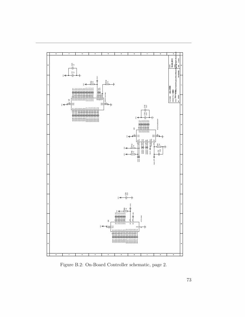
AB
CD
EF
GH
JK
BC
DE
FG
HJ
KA
FILE NAME:
BY:
DATE:
PAGE:
obc.DSN
Memories
19.06.2011
<NONE>
C:\Users\Tablet\Dropbox\Skole\Master\Rapport\CD\On-Board Contro
PATH:
2of
2
REV: <NONE>
TIME:
13:06:00
DESIGN TITLE:OBC
0 1 2 4 5 6 7 8 9
0 1 2 3 4 5 6 7 8
3
9
I/O7
I/O6
I/O5
I/O4
I/O3
I/O2
I/O1
I/O0
NANDWE
NCS2
NANDOE
ADDR21
ADDR22
NWAIT
NAND_WP
R1
10k
C2
100nF
R8
10k
VCC
A0
20
A1
19
A2
18
A3
17
A4
16
A5
15
A6
14
A7
13
A8
3
A9
2
A10
31
A11
1
A12
12
A13
4
A14
5
A15
11
A16
10
A17
6
A18
7
O0
21
O1
22
O2
23
O3
25
O4
26
O5
27
O6
28
O7
29
CE
30
OE
32
GND24VPP
9
VCC8
U4
AT27LV040A
ADDR0
ADDR1
ADDR2
ADDR3
ADDR4
ADDR5
ADDR6
ADDR7
ADDR8
ADDR9
ADDR10
ADDR11
ADDR12
ADDR13
ADDR14
ADDR15
ADDR16
ADDR17
ADDR18
I/O0
I/O1
I/O2
I/O3
I/O4
I/O5
I/O6
I/O7
VCC
NCS0
NRD
R9
10k
VCC
C18
100nF
C19
100nF
C20
100nF
VCC
VCC
A0
5
A1
4
A2
3
A3
2
A4
1
A5
48
A6
47
A7
46
A8
45
A9
30
A10
29
A11
28
A12
27
A13
26
A14
25
A15
24
A16
23
A17
22
A18
21
A19
20
I/O0
8
I/O1
9
I/O2
10
I/O3
11
I/O5
15
I/O4
14
I/O6
16
I/O7
17
I/O8
32
I/O9
33
I/O10
34
I/O11
35
I/O12
38
I/O13
39
I/O14
40
I/O15
41
CE
7
OE
44
WE
18
UB
43
LB
42
VDD12
GND13
GND37
VDD36
U2
IS61WV102416BLL
VCC
I/O0
I/O1
I/O2
I/O3
I/O4
I/O5
I/O6
I/O7
I/O8
I/O9
I/O10
I/O11
I/O12
I/O13
I/O14
I/O15
ADDR0
ADDR1
ADDR2
ADDR3
ADDR4
ADDR5
ADDR6
ADDR7
ADDR8
ADDR9
ADDR10
ADDR11
ADDR12
ADDR13
ADDR14
ADDR15
ADDR16
ADDR17
ADDR18
ADDR19
NCS1
NRD
NWR
R2
10k
VCC
R10
10k
C1
1nF
C21
1nF
VCC
ALE
17
CLE
16
CE
9
CE2
10
RE
8
WE
18
WP
19
R/B
7
R/B2
6
VCC12
VCC37
GND13
GND36
I/O0
29
I/O1
30
I/O2
31
I/O3
32
I/O4
41
I/O5
42
I/O6
43
I/O7
44
U3
MT29F16G08DAAWP
R12
10k
NCS3
VCC
VCC
Figure B.2: On-Board Controller schematic, page 2.
73

74

Appendix C
Wireless InternalCommunication Module
The source drawings for the hardware of the design is located in this section.
75

Appendix C. Wireless Internal Communication Module
P0.1
1
VDD2
DEC1
3DEC2
4
PROG
5
VSS6
VDD18
VSS17
ANT2
16
ANT1
15
VDD_PA
14
RESET
13
P0.0
24
XC1
23
XC2
22
VDD21
VSS20
IREF
19
VDD7
P0.2
8
P0.3
9
P0.4
10
P0.5
11
P0.6
12
VSS25
U1
NRF24LE1D
C1
1.5pF
L1
8.2nHL2
3.9nH
L3
2.7nH
C2
1.0pF
C3
4.7pF
C4
2.2nF
VCC
C5
33nF
C6
100nF
R1
22k
C7
18pF
C8
18pF
R2
10k
R3
10k
PROG
RESET
P0.0
P0.1
P0.2
P0.3
P0.4
P0.5
P0.6
X2
ABM8G-16
ABM8H-16.000MHZ-B4Y-T
RESET
PROG
VCC
12
J2
CONN-SIL2
VCC
PROG
RESET
P0.2
P0.3
P0.4
P0.5
1 2
J1
CONN-SIL2
1 2 3 4 5 6
J3
CONN-SIL6
12
X1
CRYSTAL
FC-13F, 32.768kHz, 12.5pF
C9
10pF
C1010pF
P0.0
P0.1
C11
1nF
VCC
VCC
C12
100nF
VCC
1
A1
ANCV12G44SAA127
Figure C.1: Intra-satellite Communication Module schematic.
76