these specification sheets are the proprietary product of ... · ld-12x07-2 1. application this...
TRANSCRIPT


LD-12X07-1
These specification sheets are the proprietary product of SHARP CORPORATION(”SHARP) and include
materials protected under copyright of SHARP. Do not reproduce or cause any third party to reproduce them
in any form or by any means, electronic or mechanical, for any purpose, in whole or in part, without the
express written permission of SHARP.
The device listed in these specification sheets was designed and manufactured for use in OA equipment.
In case of using the device for applications such as control and safety equipment for transportation(aircraft,
trains, automobiles, etc. ), rescue and security equipment and various safety related equipment which require
higher reliability and safety, take into consideration that appropriate measures such as fail-safe functions and
redundant system design should be taken.
Do not use the device for equipment that requires an extreme level of reliability, such as aerospace
applications, telecommunication equipment(trunk lines), nuclear power control equipment and medical or
other equipment for life support.
SHARP assumes no responsibility for any damage resulting from the use of the device which does not
comply with the instructions and the precautions specified in these specification sheets.
Contact and consult with a SHARP sales representative for any questions about this device.
LD-12X07-2
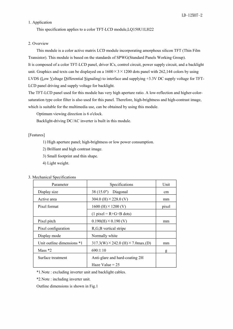
1. Application
This specification applies to a color TFT-LCD module,LQ150U1LH22
2. Overview
This module is a color active matrix LCD module incorporating amorphous silicon TFT (Thin Film
Transistor). This module is based on the standards of SPWG(Standard Panels Working Group).
It is composed of a color TFT-LCD panel, driver ICs, control circuit, power supply circuit, and a backlight
unit. Graphics and texts can be displayed on a 1600×3×1200 dots panel with 262,144 colors by using
LVDS (Low Voltage Differential Signaling) to interface and supplying +3.3V DC supply voltage for TFT-
LCD panel driving and supply voltage for backlight.
The TFT-LCD panel used for this module has very high aperture ratio. A low-reflection and higher-color-
saturation type color filter is also used for this panel. Therefore, high-brightness and high-contrast image,
which is suitable for the multimedia use, can be obtained by using this module.
Optimum viewing direction is 6 o'clock.
Backlight-driving DC/AC inverter is built in this module.
[Features]
1) High aperture panel; high-brightness or low power consumption.
2) Brilliant and high contrast image.
3) Small footprint and thin shape.
4) Light weight.
3. Mechanical Specifications
Parameter Specifications Unit
Display size 38 (15.0") Diagonal cm
Active area 304.0 (H)×228.0 (V) mm
Pixel format 1600 (H)×1200 (V) pixel
(1 pixel = R+G+B dots)
Pixel pitch 0.190(H)×0.190 (V) mm
Pixel configuration R,G,B vertical stripe
Display mode Normally white
Unit outline dimensions *1 317.3(W)×242.0 (H)×7.0max.(D) mm
Mass *2 690±10 g
Surface treatment Anti-glare and hard-coating 2H
Haze Value = 25
*1.Note : excluding inverter unit and backlight cables.
*2.Note : including inverter unit.
Outline dimensions is shown in Fig.1

LD-12X07-3
4. Input Terminals
4-1. TFT-LCD panel driving
CN1 (LVDS signals and +3.3V DC power supply)
Using connector : FI-XB30S-HF10 (JAE)
Corresponding connector : FI-X30M, or FI-X30H (JAE) Pin No. Symbol Function Remark
1 GND 2 Vcc +3.3V power supply 3 Vcc +3.3V power supply 4 Vedid DCC +3.3V power supply 5 NC Reserved 6 CLKedid DDC Clock 7 DATAedid DDC Data 8 R1IN0- Receiver signal of A side pixels (-) LVDS 9 R1IN0+ Receiver signal of A side pixels (+) LVDS 10 GND 11 R1IN1- Receiver signal of A side pixels (-) LVDS 12 R1IN1+ Receiver signal of A side pixels (+) LVDS 13 GND 14 R1IN2- Receiver signal of A side pixels (-) LVDS 15 R1IN2+ Receiver signal of A side pixels (+) LVDS 16 GND 17 CK1IN- Clock signal of A side pixels (-) LVDS 18 CK1IN+ Clock signal of A side pixels (+) LVDS 19 GND 20 R2IN0- Receiver signal of B side pixels (-) LVDS 21 R2IN0+ Receiver signal of B side pixels (+) LVDS 22 GND 23 R2IN1- Receiver signal of B side pixels (-) LVDS 24 R2IN1+ Receiver signal of B side pixels (+) LVDS 25 GND 26 R2IN2- Receiver signal of B side pixels (-) LVDS 27 R2IN2+ Receiver signal of B side pixels (+) LVDS 28 GND 29 CK2IN- Clock signal of B side pixels (-) LVDS 30 CK2IN+ Clock signal of B side pixels (+) LVDS
【Note 1】Relation between LVDS signals and actual data shows below section (4-2).
【Note 2】The shielding case is connected with signal GND.
.

LD-12X07-4
4-2 Interface block diagram
Using receiver:(THC63LVDF64A(THINE))、Corresponding Transmitter:THC63LVDM63A (THINE), DS90C363,DS90C383(National semiconductor)
TxIN12~TxIN17
TxIN 0~TxIN 5
TxIN 6~TxIN11
TxIN12~TxIN17
TxIN 0~TxIN 5
TxIN 6~TxIN11 R10~R15
B10~B15
(Hsync) (Vsync) ENAB
G10~G15
R20~R25
B20~B25
G20~G25
TTL parallel → LVDS
R1IN0+(9)
R1IN0-(8)
TxIN18
TxIN19
TxIN20
6
6
6
PLL
TxIN18
TxIN19
TxCLK IN
6
6
6
Controller
TTL parallel→ LVDS
PLL
THC63LVDM63A
THC63LVDM63A
LVDS → TTL parallel
LVDS → TTL parallel
PLL
THC63LVDF64A
PLL
THC63LVDF64A
R1IN1+(12)
R1IN1-(11)
R1IN2+(15)
R1IN2-(14)
CK1IN+(18)
CK1IN-(17)
R2IN0+(21)
R2IN0-(20)
R2IN1+(24)
R2IN1-(23)
R2IN2+(27)
R2IN2-(26)
CK2IN+(30)
CK2IN-(29)
6
6
6 RxOUT12~RxOUT17
RxOUT18
RxOUT19
RxOUT20
RxOUT 0~RxOUT 5
RxOUT 6~RxOUT11
6
6
6 RxOUT12~RxOUT17
RxOUT18
RxOUT19
RxOUT20
RxOUT 0~RxOUT 5
RxOUT 6~RxOUT11
R10~R15
B10~B15
(Hsync) (Vsync) ENAB1
G10~G15
R20~R25
B20~B25
Reserved Reserved (ENAB2)
G20~G25
Internal circuits
RxCLK OUT CK1
RxCLK OUT CK2
CLK TxCLK IN
Symbol of CN1 (Pin No.)
(Computer side)
A side pixels B side pixels
TxIN 18~20 must be fixed “Low”.
(TFT-LCD side)
TxIN20

LD-12X07-5
4-3. Inverter connector pin assign
CN2 : (Inverter signals and Inverter Power Supply)
Using connector : 52207-1690 (molex)
Pin no. Symbol Function
1,2,3 VIN Inverter power supply voltage
4,5,6 GND Gnd
7 VBB Base of Brightness control voltage
8 VBC Brightness control IC supply voltage
9 SDA Brightness control serial data signal
10 SCL Brightness control serial clock signal
11 FPVEE Backlighgt on/off signal
12 N.C. This is electrically opened
13 PANEL_ID3 Panel identity bit3 =0
14 PANEL_ID2 Panel identity bit2 =1
15 PANEL_ID1 Panel identity bit1 =0
16 PANEL_ID0 Panel identity bit0 =1
Applicable recommended FPC layout:
5. Absolute Maximum Ratings
Parameter Symbol Condition Ratings Unit Remark
Input voltage VI Ta=25℃ -0.3 ~ Vcc+0.3 V 【Note1】
+3.3V supply voltage Vcc Ta=25℃ 0 ~ + 4 V
Storage temperature Tstg - -25 ~ +60 ℃ 【Note2】
Operating temperature Topa - 0 ~ +50 ℃
Inverter supply voltage VIN Ta=25℃ 0 ~ +25 V
Inverter signals VBB,VBC
SDA,SCL
FPVEE
Ta=25℃ -0.3~ +6.8 V
2.7 min.
(N=16) All dimensions are in millimeters.

LD-12X07-6
【Note1】LVDS signals
【Note2】Humidity:95%RH Max. at Ta≦40℃.
Maximum wet-bulb temperature at 39℃ or less at Ta>40℃.
No condensation.
6. Electrical Characteristics
6-1.TFT-LCD panel driving Ta=25℃ Parameter Symbol Min. Typ. Max. Unit Remark
Vcc Supply voltage Vcc +3.0 +3.3 +3.6 V 【Note2】 Current dissipation Icc - 730 1210 mA 【Note3】 Permissive input ripple voltage VRP - - 100 mV p-p Vcc=+3.3V Input voltage range VI 0 - 2.4 V LVDS signal Differential input High VTH - - +100 mV VCM=+1.2V threshold voltage Low VTL –100 - - mV 【Note1】 Input current (High) IOH - - ±10 μA VI=2.4V Vcc=3.6V
Input current (Low) IOL - - ±10 μA VI=0V Vcc=3.6V
Terminal resistor RT - 100 - Ω Differential input
【Note1】 VCM : Common mode voltage of LVDS driver. 【Note2】 On-off conditions for supply voltage
Vcc rise time
t1≦10 ms
On time Vcc and signal
0≦t2≦50 ms
Off time signal and Vcc
0≦t3≦50 ms
Off time Vcc
400ms≦t4
On time lamp and signal
200ms≦t5
Power sequence for Backlight is not especially specified, however it is recommended to consider some
timing difference between LVDS input and Backlight input as shown above.
If the Backlight lights on before LCD starting, or if the Backlight is kept on after LCD stopping, the
screen may look white for a moment or abnormal image may be displayed.
This is caused by variation in output signal from timing generator at LVDS input on or off. It does not
cause the damage to the LCD module.
Vcc-dip conditions 1) 2.5 V≦Vcc<3.0 V
td≦10 ms 2) Vcc<2.5 V
Vcc-dip conditions should also follow the On-off conditions for supply voltage .
t1 t2
t5
0.9Vcc 0.9Vcc
Vcc
Valid
Backlight
Signal (LVDS Interface)
0.1Vcc 0.1Vcc
0.1Vcc
t3 t4
OFF OFF
Backlight ON (Lamp)
Vcc
td
3
.
0
V
20
. 5
V

LD-12X07-7
【Note3】 Typical current situation : 16-gray-bar pattern.
Vcc=+3.3V
6-2. Inverter driving
6-2-1. Backlight characteristic
The backlight system is an edge-lighting type with single CCFT (Cold Cathode Fluorescent Tube).
The life time of the lamp are shown in the following table.
Parameter Symbol Min. Typ. Max. Unit Remark
Lamp life time LL 10000 - - Hour 【Note】
【Note】 Lamp life time is defined as the time when ① occurs in the continuous
operation under the condition of Ta = 25℃ and SDA data=00HEX.
① Brightness becomes 50 % of the original value under standard condition.
6-2-2. Recommended Operating Condition
Parameter Symbol Min. Typ Max Unit
Inverter power supply VIN 9 - 21 V
Base of brightness control VBB 4.85 5.0 5.2 V
Brightness control IC
power supply
VBC 4.5 5.0 5.5 V
Logic signals SDA,SCL
FPVEE
0 5 V
6-2-3. DC Electrical Conditions Ta=25℃
Parameter Symbol Condition Min. Typ Max Unit Remark
VIN supply current IVIN VIN=9V,VBB=5V 330 - 590 mA 【Note】
VIN=21V,VBB=5V 160 280 mA
Brightness control IC
supply current
IVBC VBC =4.5~5.5V - - 200 uA
Input voltage
low VIL VBC =4.5~5.5V - -
0.3×
VBC V
SDA
SCL Input voltage
high VIH VBC =4.5~5.5V
0.7×
VBC - - V
Input voltage
low VIL VIN=12V 0.0 0.6 V
FPVEE Input voltage
high VIH VIN=12V 3.0 5.0 V
【Note】:Brightness control from minmum to maxmaum
R G B
G S 0
R G B
G S 4
R G B
G S 8
R G B
G S 5 6
R G B
G S 6 0. . . .

LD-12X07-8
6-2-4. Power ON/OFF sequence 9 V≦Vin<21 V 10 ms ≦td
6-2-5. FPVEE ON sequence Backlight power on/off is possible with FPVEE. Make sure to have more than 0.2 second-interval between each power-on.
0.2 s ≦t1
t2 ≦ 30ms
6-2-6. The Condition of Shut Down Please refer to the figure below for the conditions that will cause the inverter shut down. If the VIN voltage is higher than 7.0V and there is no enable signal, then the inverter will shut down. When the input voltage is less than 7.0V and lasts more than 150ms, the same will happen. The enable signal has to be reset to get the inverter started again.
6-2-7. Brightness Control
SDA data Brightness Notes
00HEX Maxmum Brightness Set on power-up
01~FEHEX ↓
FFHEX Minimum Brightness
td td
FPVEE
Vin
8.5V 8.5V
FPVEE
7.0V 150ms min VIN
GND
0.6V 0.6V
3.0V
t2 t1
0V(off)
on
LD-12X07-9
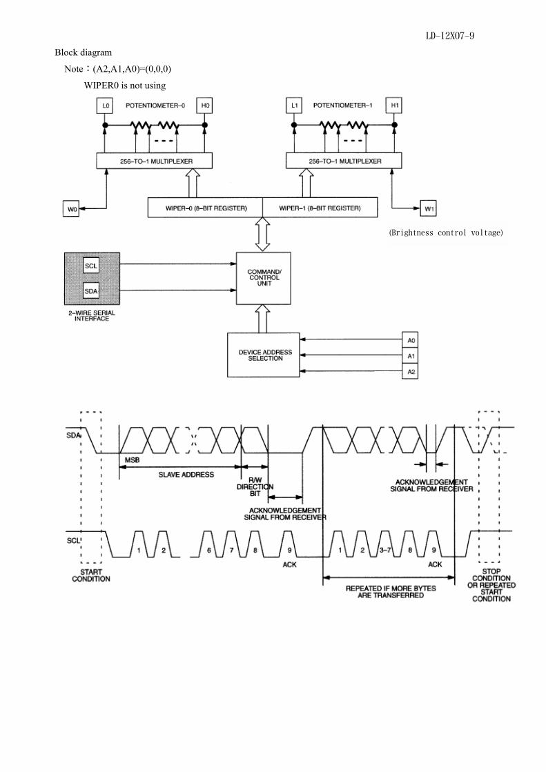
Block diagram
Note:(A2,A1,A0)=(0,0,0)
WIPER0 is not using
(Brightness control voltage)

LD-12X07-10
Brightness control byte
Brightness control data read protocols
Brightness control data wright protocols
Timing daigram

LD-12X07-11
6-2-8. AC Electrical Characteristic 0℃~50℃ VBC=5.0V
PARAMETER SYMBOL MIN. MAX UNIT NOTE
Pulse width of spikes tsp 50 ns
fast mode 0 400 1 SCL clock frequency
Standard mode fSCI
0 100 kHz
2
fast mode 1.3 BUS free time between
STOP and START condition Standard mode tBUF
4.7 us
fast mode 0.6 Hold time (Repeated)
START condition Standard mode tHD;STA
4.0 us 3
fast mode 1.3 Low Period of SCL CLOCK
Standard mode tLOW
4.7 us
fast mode 0.6 High Period of SCL
CLOCK Standard mode tHIGH
4.0 us
fast mode 0 Data hold time
Standard mode tHD;DAT
0 0.9 us
fast mode 100 Data setup time
Standard mode tSU;DAT
250 ns
fast mode 300 Rise time of both SDA and
SCL signals Standard mode tR
1000 ns
fast mode 300 Fall time of both SDA and
SCL signals Standard mode tr
300 ns
fast mode 0.6 Setup time for STOP
condition Standard mode tSU;STO
4.0 us
NOTES:
1. Fast mode.(400kHz clock rate)
2. Standard mode.(100kHz clock rate)
3. After this period, the first clock pulse is generated.
LD-12X07-12
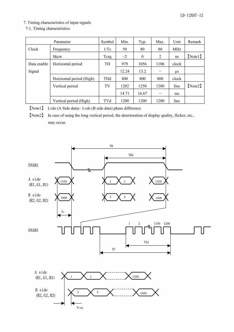
7. Timing characteristics of input signals 7-1. Timing characteristics
Parameter Symbol Min. Typ. Max. Unit Remark Clock Frequency 1/Tc 50 80 80 MHz Skew Tcsq –2 0 2 ns 【Note1】
Data enable 979 1056 1106 clock
Signal Horizontal period TH
12.24 13.2 - µs
Horizontal period (High) THd 800 800 800 clock
1202 1250 1280 line
Vertical period TV
14.71 16.67 - ms
【Note2】
Vertical period (High) TVd 1200 1200 1200 line 【Note1】 Lvds (A Side data)– Lvds (B side data) phase difference
【Note2】 In case of using the long vertical period, the deterioration of display quality, flicker, etc.,
may occur.
1599
1600
1 3
2 4
1599
1600
THd
TH
TVd
TV
Tc
1 2 1200
ENAB1
A side (R1,G1,B1)
B side (R2,G2,B2)
ENAB1 1199
1 3 1599
2 4 1600
Tcsq
A side (R1,G1,B1)
B side (R2,G2,B2)

LD-12X07-13
7-2. Input Data Signals and Display Position on the screen
1・1 1・2 1・3
2・1 2・2
3・1
1200・1
1・1600
RGB
1200・1600
R1 G1 B1 R2 G2 B2 (1・1) (1・2) Two pixels-data are sampled at the same time.
*A side : R10~R15, G10~G15, B10~B15 *B side : R20~R25, G20~G25, B20~B25
Display position of input data(V・H)

LD-12X07-14
8. Input Signals, Basic Display Colors and Gray Scale of Each Color
Colors & Data signal
Gray scale GrayScale R10 R11 R12 R13 R14 R15 G10 G11 G12 G13 G14 G15 B10 B11 B12 B13 B14 B15
R20 R21 R22 R23 R24 R25 G20 G21 G22 G23 G24 G25 B20 B21 B22 B23 B24 B25
Black - 0 0 0 0 0 0 0 0 0 0 0 0 0 0 0 0 0 0
Blue - 0 0 0 0 0 0 0 0 0 0 0 0 1 1 1 1 1 1
Green - 0 0 0 0 0 0 1 1 1 1 1 1 0 0 0 0 0 0
Cyan - 0 0 0 0 0 0 1 1 1 1 1 1 1 1 1 1 1 1
Red - 1 1 1 1 1 1 0 0 0 0 0 0 0 0 0 0 0 0
Magenta - 1 1 1 1 1 1 0 0 0 0 0 0 1 1 1 1 1 1
Yellow - 1 1 1 1 1 1 1 1 1 1 1 1 0 0 0 0 0 0
White - 1 1 1 1 1 1 1 1 1 1 1 1 1 1 1 1 1 1
Black GS0 0 0 0 0 0 0 0 0 0 0 0 0 0 0 0 0 0 0
! GS1 1 0 0 0 0 0 0 0 0 0 0 0 0 0 0 0 0 0
Darker GS2 0 1 0 0 0 0 0 0 0 0 0 0 0 0 0 0 0 0
! " " " "
# " " " "
Brighter GS61 1 0 1 1 1 1 0 0 0 0 0 0 0 0 0 0 0 0
# GS62 0 1 1 1 1 1 0 0 0 0 0 0 0 0 0 0 0 0
Red GS63 1 1 1 1 1 1 0 0 0 0 0 0 0 0 0 0 0 0
Black GS0 0 0 0 0 0 0 0 0 0 0 0 0 0 0 0 0 0 0
! GS1 0 0 0 0 0 0 1 0 0 0 0 0 0 0 0 0 0 0
Darker GS2 0 0 0 0 0 0 0 1 0 0 0 0 0 0 0 0 0 0
! " " " "
# " " " "
Brighter GS61 0 0 0 0 0 0 1 0 1 1 1 1 0 0 0 0 0 0
# GS62 0 0 0 0 0 0 0 1 1 1 1 1 0 0 0 0 0 0
Green GS63 0 0 0 0 0 0 1 1 1 1 1 1 0 0 0 0 0 0
Black GS0 0 0 0 0 0 0 0 0 0 0 0 0 0 0 0 0 0 0
! GS1 0 0 0 0 0 0 0 0 0 0 0 0 1 0 0 0 0 0
Darker GS2 0 0 0 0 0 0 0 0 0 0 0 0 0 1 0 0 0 0
! " " " "
# " " " "
Brighter GS61 0 0 0 0 0 0 0 0 0 0 0 0 1 0 1 1 1 1
# GS62 0 0 0 0 0 0 0 0 0 0 0 0 0 1 1 1 1 1
Blue GS63 0 0 0 0 0 0 0 0 0 0 0 0 1 1 1 1 1 1
0 : Low level voltage, 1 : High level voltage
Each basic color can be displayed in 64 gray scales from 6 bit data signals. According to the combination of
total 18 bit data signals, the 262,144-color display can be achieved on the screen.
Basic C
olor Gray
Scale of R
ed Gray
Scale of G
reen Gray
Scale of B
lue

LD-12X07-15
9. EDID data structure
This is the EDID(Extended Display Identification Data) data formats to support displays as defined in the VESA Plug & Display . Byte
(decimal)
Byte (hex)
Field Name and Comments Value (hex)
Value (binary)
0 00 Header 00 00000000
1 01 Header FF 11111111
2 02 Header FF 11111111
3 03 Header FF 11111111
4 04 Header FF 11111111
5 05 Header FF 11111111
6 06 Header FF 11111111
7 07 Header 00 00000000
8 08 EISA manufacture code = SHP 4D 01001101
9 09 EISA manufacture code (Compressed ASCII) 10 00010000
10 0A Product code (LQ150U1LH22 : ”5002”) 8A 10001010
11 0B Product code (hex,LSB first) 13 00010011
12 0C LCD module Serial No (fixed “0”) 00 00000000
13 0D LCD module Serial No (fixed “0”) 00 00000000
14 0E LCD module Serial No (fixed “0”) 00 00000000
15 0F LCD module Serial No (fixed “0”) 00 00000000
16 10 Week of manufacture (fixed “0”) 00 00000000
17 11 Year of manufacture - 1990 (ex 2000 – 1990 = 10) (fixed “0”) 00 00000000
18 12 EDID structure version # = 1 01 00000001
19 13 EDID revision # = 3 03 00000011
20 14 Video i/p definition = Digital i/p 80 10000000
21 15 Max H image size(cm) = 30cm 1E 00011110
22 16 Max V image size(cm) = 23cm 17 00010111
23 17 Display gamma (2.2×100) – 100 = 120 78 01111000
24 18 Feature support(stanby,suspend,RGB color/Prefer Time) CA 11001010
25 19 Red/Green Low bit(RxRy/GxGy) EC 11101100
26 1A Blue/White Low bit(BxBy/WxWy) 50 01010000
27 1B Red X(Rx) (written value “0.605”) 9A 10011010
28 1C Red Y(Ry) (written value “0.319”) 51 01010001
29 1D Green X(Gx) (written value “0.296”) 4B 01001011
30 1E Green Y(Gy) (written value “0.571”) 92 10010010
31 1F Blue X(Bx) (written value “0.138”) 23 00100011
32 20 Blue Y(By) (written value “0.134”) 22 00100010
33 21 White X(Wx) (written value “0.313”) 50 01010000
34 22 White Y(Wy) (written value “0.329”) 54 01010100
35 23 Established timings 1 (800×600@60Hz) 00 00000000
36 24 Established timings 2 (1024×768@60Hz) 00 00000000
37 25 Established timings 3(Manufacture’s reserved timing) 00 00000000
38 26 Standard timing ID1 (Horizontal active pixels) A9 10101001
39 27 Standard timing ID1 (Aspect ratio 4:3) 40 01000000

LD-12X07-16
40 28 Standard timing ID2 01 00000001
41 29 Standard timing ID2 01 00000001
42 2A Standard timing ID3 01 00000001
43 2B Standard timing ID3 01 00000001
44 2C Standard timing ID4 01 00000001
45 2D Standard timing ID4 01 00000001
46 2E Standard timing ID5 01 00000001
47 2F Standard timing ID5 01 00000001
48 30 Standard timing ID6 01 00000001
49 31 Standard timing ID6 01 00000001
50 32 Standard timing ID7 01 00000001
51 33 Standard timing ID7 01 00000001
52 34 Standard timing ID8 01 00000001
53 35 Standard timing ID8 01 00000001
54 36 Detailed timing descriptor#1 fck/10000 = 16000=3E80h 80 10000000
55 37 #1 fck 3E 00111110
56 38 #1 Horizontal active 1600 = 640h “40” 40 01000000
57 39 #1 Horizontal blanking 512 = 200h “00” 00 00000000
58 3A #1 Horizontal active/Horizontal blanking “62h” 62 01100010
59 3B #1 Vertical active 1200 = 4B0h “B0” B0 10110000
60 3C #1 Vertical blanking 50 = 032h “32” 32 00110010
61 3D #1 Vertical active/Vertical blanking “40h” 40 01000000
62 3E #1 Horizontal sync , offset 64 = 040h “40” 40 01000000
63 3F #1 Horizontal sync , width 192 = 0C0h “C0” C0 11000000
64 40 #1 Vertical sync,offset / Vertical sync,width 13 00010011
65 41 #1 Horizontal sync offset/width/Vertical sync offset/width 00 00000000
66 42 #1 Horizontal image size 304mm = 130h “30” 30 00110000
67 43 #1 Vertical image size 228mm = 0E4h “E4” E4 11100100
68 44 #1 Horizontal image size / Vertical image size 10 00010000
69 45 Horizontal boader 00 00000000
70 46 Vertical boader 00 00000000
71 47 Flags 18 00011000
72 48 Detailed timing descriptor #2 00 00000000
73 49 Flag 00 00000000
74 4A Reserved 00 00000000
75 4B Dummy Descriptor 10 00010000
76 4C Flag 00 00000000
77 4D 1st dummy 00 00000000
78 4E 2nd dummy 00 00000000
79 4F 3rd dummy 00 00000000
80 50 4th dummy 00 00000000
81 51 5th dummy 00 00000000
82 52 6th dummy 00 00000000
83 53 7th dummy 00 00000000
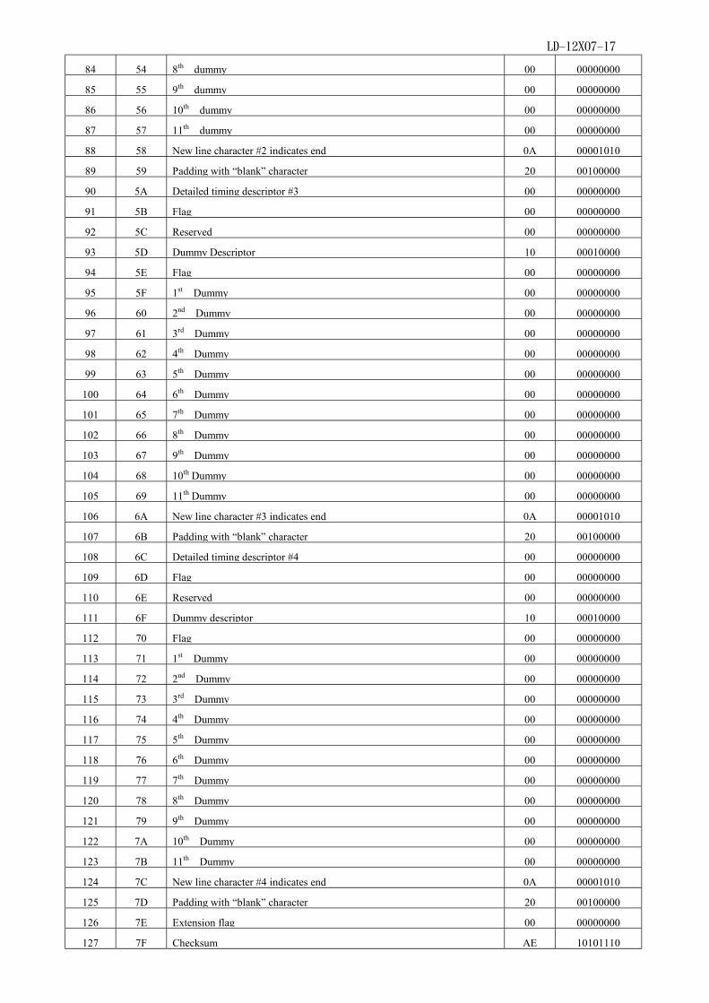
LD-12X07-17
84 54 8th dummy 00 00000000
85 55 9th dummy 00 00000000
86 56 10th dummy 00 00000000
87 57 11th dummy 00 00000000
88 58 New line character #2 indicates end 0A 00001010
89 59 Padding with “blank” character 20 00100000
90 5A Detailed timing descriptor #3 00 00000000
91 5B Flag 00 00000000
92 5C Reserved 00 00000000
93 5D Dummy Descriptor 10 00010000
94 5E Flag 00 00000000
95 5F 1st Dummy 00 00000000
96 60 2nd Dummy 00 00000000
97 61 3rd Dummy 00 00000000
98 62 4th Dummy 00 00000000
99 63 5th Dummy 00 00000000
100 64 6th Dummy 00 00000000
101 65 7th Dummy 00 00000000
102 66 8th Dummy 00 00000000
103 67 9th Dummy 00 00000000
104 68 10th Dummy 00 00000000
105 69 11th Dummy 00 00000000
106 6A New line character #3 indicates end 0A 00001010
107 6B Padding with “blank” character 20 00100000
108 6C Detailed timing descriptor #4 00 00000000
109 6D Flag 00 00000000
110 6E Reserved 00 00000000
111 6F Dummy descriptor 10 00010000
112 70 Flag 00 00000000
113 71 1st Dummy 00 00000000
114 72 2nd Dummy 00 00000000
115 73 3rd Dummy 00 00000000
116 74 4th Dummy 00 00000000
117 75 5th Dummy 00 00000000
118 76 6th Dummy 00 00000000
119 77 7th Dummy 00 00000000
120 78 8th Dummy 00 00000000
121 79 9th Dummy 00 00000000
122 7A 10th Dummy 00 00000000
123 7B 11th Dummy 00 00000000
124 7C New line character #4 indicates end 0A 00001010
125 7D Padding with “blank” character 20 00100000
126 7E Extension flag 00 00000000
127 7F Checksum AE 10101110

LD-12X07-18
10. Optical Characteristics
Ta=25℃, Vcc=+3.3V
Parameter Symbol Condition Min. Typ. Max. Unit Remark
Viewing Horizontal θ21,θ22 CR>10 45 - - Deg. 【Note1,4】
angle Vertical θ11 10 - - Deg.
range θ12 30 - - Deg.
Contrast ratio CRn θ=0° 150 - - 【Note2,4】
CRo Optimum viewing angle - 300 -
Response Rise Τr θ=0° - 15 ms 【Note3,4】
time Decay Τd - 30 ms
Chromaticity of x - 0.313 - 【Note4】
white y - 0.329 -
【Note4】 YL2 120 150 - cd/m2 Vin= 21V
SDA=00HEX
White Uniformity δW - - 1.45 【Note5】
※ The measurement shall be executed 30 minutes after lighting at rating. (typical condition: SDA=00HEX)
The optical characteristics shall be measured in a dark room or equivalent state with the method shown in Fig.2 below. Photodetector (BM-5A:TOPCON)
Fig.2 Optical characteristics measurement methodCenter of the screen
TFT-LCD module
400mm
Field=2°
LCD panel

LD-12X07-19
【Note1】Definitions of viewing angle range:
【Note2】Definition of contrast ratio:
The contrast ratio is defined as the following.
Contrast Ratio (CR) =
【Note3】Definition of response time:
The response time is defined as the following figure and shall be measured by
switching the input signal for "black" and "white" .
【Note4】This shall be measured at center of the screen.
【Note5】Definition of white uniformity:
White uniformity is defined as the
following with five measurements
(A~E).
Luminance (brightness) with all pixels white
Luminance (brightness) with all pixels black
Maximum Luminance of five points (brightness)Minimum Luminance of five points (brightness)
δw=
DDDD AAAA
CCCC
EEEE
BBBB
1200 pixel 800 400
300
600
Pixel 900

LD-12X07-20
11. Display Quality
The display quality of the color TFT-LCD module shall be in compliance with the Incoming
Inspection Standard.
12.Handling Precautions
a) Be sure to turn off the power supply when inserting or disconnecting the cable.
b) Be sure to design the cabinet so that the module can be installed without any extra stress such as
warp or twist.
c) Since the front polarizer is easily damaged, pay attention not to scratch it.
d) Wipe off water drop immediately. Long contact with water may cause discoloration or spots.
e) When the panel surface is soiled, wipe it with absorbent cotton or other soft cloth.
f) Since the panel is made of glass, it may break or crack if dropped or bumped on hard surface.
Handle with care.
g) Since CMOS LSI is used in this module, take care of static electricity and injure the human earth
when handling.
h) Observe all other precautionary requirements in handling components.
i) This module has its circuitry PCBs on the rear side and should be handled carefully in order not
to be stressed.
j) Laminated film is attached to the module surface to prevent it from being scratched . Peel the
film off slowly just before the use with strict attention to electrostatic charges. Ionized air shall
be blown over during the action. Blow off the 'dust' on the polarizer by using an ionized nitrogen
gun, etc..
13. Packing form ( See Fig.3)
a) Piling number of cartons : 5 cartons
b) Package quantity in one carton : 10 pcs
c) Carton size : 438(W)×372(D)×307(H)mm
d) Total mass of one carton filled with full modules : 8400g

LD-12X07-21
14.Reliability test items
No. Test item Conditions
1 High temperature storage test Ta = 60℃ 240h
2 Low temperature storage test Ta = -25℃ 240h
3 High temperature
& high humidity operation test
Ta = 40℃ ; 95 %RH 240h
(No condensation)
4 High temperature operation test Ta = 50℃ 240h
(The panel temp. must be less than 60℃)
5 Low temperature operation test Ta = 0℃ 240h
6 Vibration test
(non- operating)
Frequency : 10~57Hz/Vibration width (one side):0.075mm
: 58~500Hz/Gravity:9.8m/s2
Sweep time : 11 minutes
Test period : 3 hours
(1 hour for each direction of X,Y,Z)
7 Shock test
(non- operating)
Max. gravity : 490 m/s2
Pulse width : 11 ms, sine wave
Direction : ±X,±Y,±Z
once for each direction.
LD-12X07-22
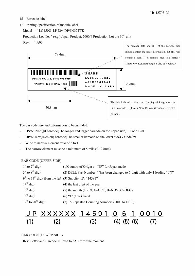
15.Bar code label
1) Printing Specification of module label
Model :LQ150U1LH22…DP/N037TTK
Production Lot No.:(e.g.) Japan Product, 2000/6 Production Lot the 10th unit
Rev. :A00
79.4mm
12.7mm
50.8mm
The bar code size and information to be included:
- DS/N: 20-digit barcode(The longer and larger barcode on the upper side):Code 128B
- DP/N: Rev(revision) barcode(The smaller barcode on the lower side):Code 39
- Wide to narrow element ratio of 3 to 1
- The narrow element must be a minimum of 5 mils (0.127mm)
BAR CODE (UPPER SIDE)
1st to 2th digit (1)Country of Origin : “JP” for Japan made
3st to 8th digit (2) DELL Part Number: “(has been changed to 6-digit with only 1 leading “0”)”
9th to 13th digit from the left (3) Supplier ID: “14591”
14th digit (4) the last digit of the year
15th digit (5) the month (1 to 9, A=OCT, B=NOV, C=DEC)
16th digit (6) “1” (One) fixed
17th to 20nd digit (7) 16 Repeated Counting Numbers (0000 to FFFF)
JPJPJPJP XXXXXXXXXXXXXXXXXXXXXXXX 14591145911459114591 0000 6666 1111 0010001000100010 (1) (2) (1) (2) (1) (2) (1) (2) (3) (4)(5)(6) (7) (3) (4)(5)(6) (7) (3) (4)(5)(6) (7) (3) (4)(5)(6) (7) BAR CODE (LOWER SIDE)
Rev: Letter and Barcode = Fixed to “A00” for the moment
SHARPSHARPSHARPSHARP LQ150U1LHLQ150U1LHLQ150U1LHLQ150U1LH22222222 DS/N JP-037TTK-14591-071-0010
DP/N 037TTK |C/0 JP|Rev.A00
The barcode data and HRI of the barcode data
should contain the same information, but HRI will
contain a dash (-) to separate each field. (HRI =
Times New Roman (Font) at a size of 7 points.)
The label should show the Country of Origin of the
LCD module. (Times New Roman (Font) at size of 8
points.)
*06Z00010A**06Z00010A**06Z00010A**06Z00010A*
MADEMADEMADEMADE ININININ JAPAJAPAJAPAJAPA

LD-12X07-23
The right side of the bar code label shows Sharp’s Specification:
SHARPSHARPSHARPSHARP
LQ150U1LH22 Model No. *06Z00001A* Production Lot No. MADE IN JAPAN
2) Printing Specification of packing label
[1] Supplier Name [HRI]
[2] Dell Part Number[HRI]
[3] Dell Part Number[Barcode]:Code128B
- LQ150U1LH22 037TTK
[4] Box Quantity[HRI]
[5] Box Quantity[Barcode(Lower Left Side)]:Code 128B
- LQ150U1LH22 10
[6] Country of Origin[HRI]
[7] Country of Origin[Barcode(Lower right Side)]:Code 128B
- Japan JP
16.Others
1) Adjusting volume have been set optimally before shipment, so do not change any adjusted value.
If adjusted value is changed, the technical literature may not be satisfied.
2) Disassembling the module can cause permanent damage and should be strictly avoided.
3) Please be careful since image retention may occur when a fixed pattern is displayed for a long time.
4) If any problem occurs in relation to the description of this specification, it shall be resolved through
discussion with spirit of cooperation.
76.2mm
76.2mm
SHARP CORPORATION
DP/N 037TTK
Box Qty 10 C/O – JP
[1]
[2]
[4]
[5]
[3]
[6]
[7]
LD-12X07-24
Fig3-1. Packing Form

LD-12X07-25
Fig3-2. Location of barcode label attachment
SHARP Package
Barcode Label Shipping carton
Japan product
TYPE
QUANTITY
LOT(DATE)
社内品番:(4S)LQ150U1LH22
LotNO.:1T)2000.10.01
Quantity:(Q)10 pcs
ユーザー品番:
シャープ物流用ラベルです。
Dell Package
Barcode Label

LD-12X07-26
Fig1. Outline Dimensions

