thermal conductivity of iii-v semiconductor...
TRANSCRIPT

Thermal conductivity of III-V semiconductor superlatticesS. Mei and I. Knezevic Citation: Journal of Applied Physics 118, 175101 (2015); doi: 10.1063/1.4935142 View online: http://dx.doi.org/10.1063/1.4935142 View Table of Contents: http://scitation.aip.org/content/aip/journal/jap/118/17?ver=pdfcov Published by the AIP Publishing Articles you may be interested in Thermal conduction in lattice–matched superlattices of InGaAs/InAlAs Appl. Phys. Lett. 105, 051909 (2014); 10.1063/1.4892575 Analytical expression for thermal conductivity of superlattices J. Appl. Phys. 107, 084303 (2010); 10.1063/1.3386464 Thermal conductivity of Si/SiGe superlattice films J. Appl. Phys. 104, 114301 (2008); 10.1063/1.3032602 Lattice thermal conductivity of group-IV and III–V semiconductor alloys J. Appl. Phys. 102, 063502 (2007); 10.1063/1.2779259 Thermoelectric figure of merit and maximum power factor in III–V semiconductor nanowires Appl. Phys. Lett. 84, 2652 (2004); 10.1063/1.1695629
[This article is copyrighted as indicated in the article. Reuse of AIP content is subject to the terms at: http://scitation.aip.org/termsconditions. Downloaded to ] IP:
104.159.208.7 On: Wed, 02 Dec 2015 02:00:47

Thermal conductivity of III-V semiconductor superlattices
S. Meia) and I. Knezevicb)
Department of Electrical and Computer Engineering, University of Wisconsin-Madison, Madison,Wisconsin 53706, USA
(Received 14 August 2015; accepted 22 October 2015; published online 3 November 2015)
This paper presents a semiclassical model for the anisotropic thermal transport in III-V semicon-
ductor superlattices (SLs). An effective interface rms roughness is the only adjustable parameter.
Thermal transport inside a layer is described by the Boltzmann transport equation in the relaxation
time approximation and is affected by the relevant scattering mechanisms (three-phonon, mass-
difference, and dopant and electron scattering of phonons), as well as by diffuse scattering from the
interfaces captured via an effective interface scattering rate. The in-plane thermal conductivity is
obtained from the layer conductivities connected in parallel. The cross-plane thermal conductivity
is calculated from the layer thermal conductivities in series with one another and with thermal
boundary resistances (TBRs) associated with each interface; the TBRs dominate cross-plane trans-
port. The TBR of each interface is calculated from the transmission coefficient obtained by interpo-
lating between the acoustic mismatch model (AMM) and the diffuse mismatch model (DMM),
where the weight of the AMM transmission coefficient is the same wavelength-dependent
specularity parameter related to the effective interface rms roughness that is commonly used to
describe diffuse interface scattering. The model is applied to multiple III-arsenide superlattices,
and the results are in very good agreement with experimental findings. The method is both simple
and accurate, easy to implement, and applicable to complicated SL systems, such as the active
regions of quantum cascade lasers. It is also valid for other SL material systems with high-quality
interfaces and predominantly incoherent phonon transport. VC 2015 AIP Publishing LLC.
[http://dx.doi.org/10.1063/1.4935142]
I. INTRODUCTION
Nanoscale thermal transport is of considerable impor-
tance in the operation of modern electronic, optoelectronic,
and thermoelectric devices.1,2 In superlattices (SLs), multiple
interfaces between different materials play a critical role in
the thermal transport.2,3 Advanced experimental techniques
have enabled the measurements of the in-plane4 and cross-
plane5,6 thermal conductivity in SLs. Experiments show that
the thermal conductivity of SLs is anisotropic and consider-
ably lower than that of the constituent bulk materials.7–16
Theoretical studies find that the diffuse interface scattering is
responsible for lowering of the in-plane (and, in part, the
cross-plane) thermal conductivity, while the thermal bound-
ary resistance (TBR) between adjacent layers is a key factor
in the cross-plane thermal-conductivity reduction.2,3,17,18
Superlattices based on III-V compound semiconductors
have widespread use in optoelectronics.19,20 In quantum cas-
cade lasers (QCLs), self-heating is the main issue limiting
the development of room-temperature (RT) continuous-wave
lasing, which is exacerbated by the poor thermal conduction
through hundreds of interfaces in a typical structure.14,21,22
A good understanding of the influence of interfaces on the
thermal conductivity tensor of III-V SLs would enable
advances in the design and modeling and optoelectronic
devices for enhanced reliability.
The interfacial transport behavior is largely dependent
on the material system and interface quality.2 The acoustic
mismatch model (AMM) and the diffuse mismatch model
(DMM) have been traditionally used to calculate the phonon
transmission coefficient and the resulting TBR of an inter-
face.23,24 These two models yield the lower and upper limits
of the TBR, respectively, but do not satisfactorily explain re-
alistic experimental results.3 Molecular dynamics simula-
tions25–30 have provided valuable insights into heat transport
across a number of solid-solid interfaces. The non-
equilibrium Green’s function technique (NEGF) has also
been applied to describe the phonon dynamics,31,32 generally
without phonon-phonon scattering. In general, atomistic sim-
ulations are limited by computation burden, which makes it
hard to study complicated SL structures, such as the active
region of solid-state lasers.19,20
In this paper, we present a semiclassical model describ-
ing the full thermal conductivity tensor of III-V compound
SL structures and apply it to III-arsenide systems. The pho-
non transport inside each layer is captured by solving the
phonon Boltzmann transport equation (PBTE) in the
relaxation-time approximation (RTA), with rates describing
the common internal scattering mechanisms as well as the
partially diffuse scattering from the interfaces.33 The in-
plane thermal conductivity is obtained from the layers
connected in parallel, while the cross-plane conductivity is
calculated from the layers and TBRs in series. The TBR of
each interfaces is calculated by interpolating between the
AMM and the DMM transmission coefficients at the
a)Electronic mail: [email protected])Electronic mail: [email protected]
0021-8979/2015/118(17)/175101/8/$30.00 VC 2015 AIP Publishing LLC118, 175101-1
JOURNAL OF APPLIED PHYSICS 118, 175101 (2015)
[This article is copyrighted as indicated in the article. Reuse of AIP content is subject to the terms at: http://scitation.aip.org/termsconditions. Downloaded to ] IP:
104.159.208.7 On: Wed, 02 Dec 2015 02:00:47
interface. Both the partially diffuse interface scattering and
the AMM-DMM interpolation are described with the aid of
the same momentum-dependent specularity parameter, in
which there is a single adjustable parameter—an effective
interface rms roughness. The model can effectively describe
complicated systems with an arbitrary number of interfaces
and random layer thicknesses. Despite the model simplicity,
the calculation results agree well with experimental data
from multiple studies by different groups.7–10,12,15,16 The
model is also quite general: it is applicable to SLs in
other material systems with good-quality interfaces and
semiclassical phonon transport.11,13,34
This paper is organized as follows. Section II describes
the SL thermal transport model in detail: the role of interface
roughness on the baseline layer conductivity that affects both
the cross-plane and in-plane conduction, as well as the addi-
tional effect it has on cross-plane transport through the TBR.
In Sec. III, we illustrate the robustness of the transport model
by comparing our calculation results with a number of
experiments on GaAs/AlAs and InGaAs/InAlAs superlattice
systems, and we also calculate the thermal conductivity ten-
sor in a quantum cascade laser active region. We conclude
with Sec. IV. This paper is accompanied by electronic
supplementary material.35
II. THERMAL CONDUCTIVITY OF III-VSUPERLATTICES
A semiconductor SL is a periodic structure, with each
period consisting of two or more thin layers of different
materials. III-V semiconductor SLs have been widely used
in electronic and photonic devices.19,20,36,37 Experimental
results on several material systems show that the thermal
conductivity of a SL is substantially lower than that of a
weighted average of the constituent bulk materials.7–13,15,16
The thermal transport in SLs also exhibits pronounced ani-
sotropy: the cross-plane thermal conductivity (the thermal
conductivity in the SL growth direction, normal to each pla-
nar layer) is much lower than the in-plane thermal conductiv-
ity.2 Theoretical studies show that the interfaces between
adjacent layers are responsible for both the overall reduction
and the anisotropy of thermal conductivity.17,18,25 Here, we
offer a model that quantitatively captures both effects of the
interfaces.
Even though a typical layer thickness in III-V SL struc-
tures is on the order of a few nanometers, we argue that
coherent phonon transport can be neglected and that the
semiclassical phonon Boltzmann equation provides an
appropriate framework for analyzing heat flow in these sys-
tems over a range of temperatures. The reasons for this asser-
tion are the following:
1. We are interested in the thermal conductivity of SLs near
room temperature, where the phonon-phonon interaction
is strong and breaks the phonon wave coherence.34 The
phonon coherence length in bulk GaAs at room tempera-
ture has been estimated to be smaller than 2 nm (Refs. 17
and 18), and this value will be even lower in ternary com-
pounds owing to alloy scattering. Several SL structures
we consider here7–10,12,15,16 have layers of thickness
greater than or comparable to the phase-breaking length
in individual layers, which implies that transport in them
is largely incoherent. Indeed, experiments find that
coherent transport features are important in GaAs/AlAs
SLs below T< 100 K.38 In the SLs with ternary III-V
compounds, coherent transport phenomena would be im-
portant at even lower temperatures.
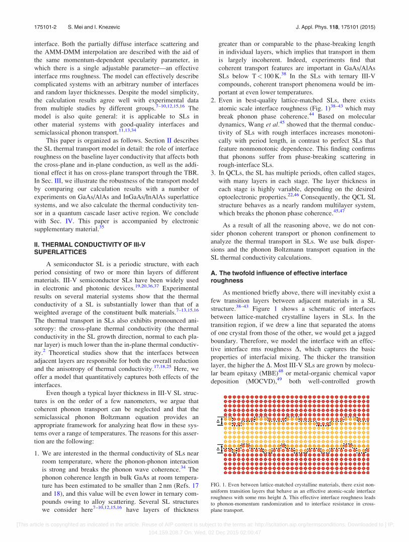
2. Even in best-quality lattice-matched SLs, there exists
atomic scale interface roughness (Fig. 1)38–43 which may
break phonon phase coherence.44 Based on molecular
dynamics, Wang et al.45 showed that the thermal conduc-
tivity of SLs with rough interfaces increases monotoni-
cally with period length, in contrast to perfect SLs that
feature nonmonotonic dependence. This finding confirms
that phonons suffer from phase-breaking scattering in
rough-interface SLs.
3. In QCLs, the SL has multiple periods, often called stages,
with many layers in each stage. The layer thickness in
each stage is highly variable, depending on the desired
optoelectronic properties.22,46 Consequently, the QCL SL
structure behaves as a nearly random multilayer system,
which breaks the phonon phase coherence.45,47
As a result of all the reasoning above, we do not con-
sider phonon coherent transport or phonon confinement to
analyze the thermal transport in SLs. We use bulk disper-
sions and the phonon Boltzmann transport equation in the
SL thermal conductivity calculations.
A. The twofold influence of effective interfaceroughness
As mentioned briefly above, there will inevitably exist a
few transition layers between adjacent materials in a SL
structure.38–43 Figure 1 shows a schematic of interfaces
between lattice-matched crystalline layers in SLs. In the
transition region, if we drew a line that separated the atoms
of one crystal from those of the other, we would get a jagged
boundary. Therefore, we model the interface with an effec-
tive interface rms roughness D, which captures the basic
properties of interfacial mixing. The thicker the transition
layer, the higher the D. Most III-V SLs are grown by molecu-
lar beam epitaxy (MBE)48 or metal-organic chemical vapor
deposition (MOCVD),49 both well-controlled growth
FIG. 1. Even between lattice-matched crystalline materials, there exist non-
uniform transition layers that behave as an effective atomic-scale interface
roughness with some rms height D. This effective interface roughness leads
to phonon-momentum randomization and to interface resistance in cross-
plane transport.
175101-2 S. Mei and I. Knezevic J. Appl. Phys. 118, 175101 (2015)
[This article is copyrighted as indicated in the article. Reuse of AIP content is subject to the terms at: http://scitation.aip.org/termsconditions. Downloaded to ] IP:
104.159.208.7 On: Wed, 02 Dec 2015 02:00:47

environments. As a result, all the interfaces in the SL should
be nearly identical. Therefore, we use a single roughness Dto model all the interfaces.
The probability of a phonon reflecting specularly from a
rough interface is represented by a wave-number-dependent
specularity parameter50
pspecð~qÞ ¼ expð�4D2j~qj2 cos2hÞ; (1)
where j~qj is the magnitude of the wave vector, and h repre-
sents the angle between ~q and the normal direction to the
interface. This expression is nominally derived in the limit
of uncorrelated roughness;50,51 but, considering that more
correlated surfaces scatter phonons more specularly,52
surface correlation can effectively be captured by using a
lowered D.53
The diffuse interface scattering affects all phonons in
the SL and influences phonon mode occupation inside each
layer.33 The effect on interface roughness on mode popula-
tion can be captured by solving the PBTE with appropriate
boundary conditions. The result is an effective interface scat-
tering rate33 that captures the interplay between internal
mechanisms (normal and umklapp three-phonon, isotope,
alloy, dopant, and electron scattering; see supplementary
material35) and interface roughness in a layer of thickness L
s�1interface ~qð Þ ¼
vb;? ~qð ÞL
Fp ~q; Lð Þ
1� sb;internal ~qð Þvb;? ~qð ÞL
Fp ~q; Lð Þ; (2a)
where
Fp ~q; Lð Þ ¼1� pspec ~qð Þ� �
f1� exp �L=sb;internal ~qð Þvb;?� �
g1� pspec ~qð Þexp �L=sb;internal ~qð Þvb;?
� � ;
(2b)
is a mode-dependent scaling factor. Here, b denotes the pho-
non branch and ~q its wave vector, vb,? is the component of
the phonon group velocity normal to the interface, and
sb;internalð~qÞ is the total relaxation time due to internal scatter-
ing mechanisms in the layer (see supplementary material35).
It is noteworthy that the effective rate of interface scattering
(2a) depends on both roughness and the relative size of the
layer thickness (L) to the mean free path for internal
scattering (sb;internalð~qÞvb;?): for very thin layers
(L=sb;internalð~qÞvb;? � 1), the phonon “sees” both interfaces
of a layer (s�1interfaceð~qÞ ! 2
vb;?ð~qÞL
1� pspecð~qÞ1þ pspecð~qÞ
, a well-known
expression derived by Ziman51), while for very thick layers
(L=sb;internalð~qÞvb;? � 1), the phonon will scatter many times
due to internal mechanisms between successive interactions
with interfaces, as if the interfaces were completely inde-
pendent (s�1interfaceð~qÞ !
vb;?ð~qÞL½1� pspecð~qÞ�). For details,
see Ref. 33. Through this additional effective scattering rate,
rough interfaces that bound each layer affect phonon popula-
tion and thus influence both the in-plane and cross-plane
thermal transport.33 This is the first aspect of interfacial
influence on the thermal transport in SLs.
The cross-plane thermal conductivity bears an additional
influence of the interfaces.24,54 In order to carry heat along
the cross-plane direction, phonons must cross interfaces. As
there are two different materials on the two sides of the inter-
face, the phonon transmission probability through the inter-
face is not unity, and a thermal boundary resistance emerges.
There have been two widely accepted models—the
AMM23,55 and the DMM—for the calculation of the phonon
transmission coefficient and the TBR.24
From the AMM point of view, the interface between
two isotropic media is treated as a perfect plane, and the pho-
nons are treated as plane waves. The AMM transmission
coefficient is the ratio of transmitted to injected heat flux and
is calculated upon solving the elastic continuum equation
with appropriate boundary conditions (continuity of the nor-
mal component of the wave number, which will yield a
Snell’s law analogue, and continuity of the velocity field and
tangential force). The AMM transmission coefficient for a
phonon going from material 1 to material 2 can be expressed
as
tAMMb;1!2 ~qð Þ ¼
4Z?b;1 ~qð ÞZ?b;2 ~qð Þ
Z?b;1 ~qð Þ þ Z?b;2 ~qð Þh i2
; (3)
where Z?b;1=2 ¼ q1=2v?b;1=2ð~qÞ are the perpendicular acoustic
impedances of sides 1 and 2. q is the mass density of a mate-
rial. Here, we work with full phonon dispersions, so it is
hard to achieve detailed balance, i.e., conserve both momen-
tum and energy for a phonon going through an interface.
However, the lattice structures and dispersion curves for III-
As are very similar, so we simply momentum and the result-
ing error in energy conservation is quite small.
On the other hand, in the DMM, the assumption is that
the coherence is completely destroyed at the interface: a pho-
non loses all memory about its velocity and randomly scat-
ters into another phonon with the same energy. The
transmission coefficient can be derived from the principle of
detailed balance as56
tDMM1!2 ~qð Þ ¼ vb;2 ~qð ÞD2 x1 ~qð Þð Þ
vb;2 ~qð ÞD2 x1 ~qð Þð Þ þ vb;1 ~qð ÞD1 x1 ~qð Þð Þ ; (4)
where D1(x) and D2(x) are the phonon densities of states in
materials 1 and 2, respectively.
In reality, for a high-quality interface like that in a III-V
SL structure, phonon interface scattering is neither purely
specular nor completely diffuse; consequently, the AMM
overestimates while the DMM underestimates the transmis-
sion coefficient.57 In order to accurately model the TBR in a
large temperature range and for various interfaces, we will
interpolate between the two models for the transmission
coefficient.18,58 We posit that the specularity parameter (1)can also be used to give weight to the probability of phonontransmission without momentum randomization, i.e., to theAMM transmission coefficient. In other words, we introduce
an effective phonon transmission coefficient as
tbð~qÞ ¼ pspecð~qÞ � tAMMb ð~qÞ þ ½1� pspecð~qÞ� � tDMM
b ð~qÞ: (5)
175101-3 S. Mei and I. Knezevic J. Appl. Phys. 118, 175101 (2015)
[This article is copyrighted as indicated in the article. Reuse of AIP content is subject to the terms at: http://scitation.aip.org/termsconditions. Downloaded to ] IP:
104.159.208.7 On: Wed, 02 Dec 2015 02:00:47

This coefficient captures both the acoustic mismatch and the
momentum randomization at a rough interface between two
media. The rougher the interface, the lower the specularity
parameter, and therefore the higher the TBR. The TBR will
only be picked up by the phonons trying to cross an inter-
face, thus having an influence on cross-plane transport only.
This is the second effect the roughness has on thermal
transport.
We note that the above discussion holds for acoustic
phonons, which are the dominant carriers of heat in semicon-
ductors. The role of optical phonons in bulk heat transport
has recently been highlighted,59 but they are relatively minor
contributors to bulk heat transport owing to the low occupa-
tion number and group velocity. It is also unclear how opti-
cal phonons behave when crossing boundaries, but it is
likely that their transmission is highly suppressed because
their existence hinges of good crystallinity. A recent paper
by Ong and Zhang supports this assertion.60 Therefore,
optical phonons are neglected in this study.
B. Calculation of in-plane and cross-plane thermalconductivities
First, each layer’s thermal conductivity is calculated in
the same way as the bulk thermal conductivity of a material
(see Sec. S-I in supplementary material35), but with an addi-
tional scattering rate (2a) due to the presence of interfaces.33
The layer thermal conductivity obtained this way will al-
ready be lower than the bulk thermal conductivity of the
same material.
Second, the TBR is calculated using a transmission
coefficient interpolated from the AMM and the DMM val-
ues. The TBR from material 1 to material 2, denoted R1!2,
is given by
R�11!2 ¼
1
2
Xb;~q
vb;1;? ~qð ÞCb;T ~qð Þt1!2 x1 ~qð Þð Þ1� 1
2ht1!2 x1 ~qð Þð Þ þ t2!1 x1 ~qð Þð Þi
: (6)
The denominator in the expression is a correction factor
introduced following the modified definition of temperature
of Simons61 and Zeng and Chen,62 as the phonon distribution
at the interface is far from equilibrium. The correction
ensures that the TBR vanishes at a fictitious interface inside
a material. Here, ht1!2ðx1ð~qÞÞ þ t2!1ðx1ð~qÞÞi represents
the average value of transmission coefficients over the
Brillouin zone.
With properly calculated layer thermal conductivity and
the TBR, the in-plane and cross-plane thermal conductivity
of a SL with two layers per period can be written as33,54
jin-plane ¼L1j1 þ L2j2
L1 þ L2
; (7a)
jcross-plane ¼L1 þ L2
L1
j1þ þL2
j2þ R1!2 þ R2!1ð Þ
; (7b)
where L1 and L2 are the layer thicknesses of materials 1 and
2, respectively, while j1 and j2 are the corresponding layer
thermal conductivities. R1!2 and R2!1 represent the TBRs
from layer 1 to layer 2 and from layer 2 to layer 1. The
expressions can be extended to the situation of a SL with nlayers of thicknesses Li (i¼ 1,…, n)
jin-plane ¼Pn
i¼1 LijiPni¼1 Li
; (7c)
jcross-plane ¼Pn
i¼1 LiPni¼1 Li=ji þ Ri!iþ1
; (7d)
with the understanding that Rn!nþ1�Rn!1, owing to peri-
odic boundary conditions (i.e., after the last layer n comes
layer 1 again). Considering that the TBRs are generally not
symmetric (Ri!j 6¼Rj!i), the cross-plane thermal conductiv-
ity is not the same in both directions, so SLs can exhibit ther-
mal rectification properties.
III. RESULTS AND COMPARISON WITH EXPERIMENTS
A. GaAs/AlAs superlattices
We have compared the results from our simple model
with several experimental results by different groups on both
the in-plane7,9,15 and cross-plane8,10,12,15,16 thermal conduc-
tivity of III-arsenide SLs and obtained good agreement.
Figure 2 shows the RT in-plane thermal conductivity of
GaAs/AlAs SLs with various layer thicknesses. To compare
with Yao’s data,7 we set the effective interface roughness to
6 A. The in-plane thermal conductivity should first increase
monotonically with increasing layer thickness, then saturate
at the average bulk value of roughly 66 W/mK. The measure-
ment is non-monotonic and appears to saturate at a lower
value, which Yao7 suggested stems from pronounced interfa-
cial mixing and thus considerable alloy scattering of phonons
between layers. We note that our model does not capture sig-
nificant interfacial mixing and is instead suitable for high
quality interfaces with only atomic-scale roughness.
Figure 3 shows the in-plane thermal conductivity of a
GaAs/AlAs SL with a layer thickness of 70 nm at various
temperatures. The symbols are the experimental results
FIG. 2. In-plane thermal conductivity of GaAs/AlAs superlattices as a func-
tion of layer thickness. Red dots are the experimental data from Ref. 7, and
blue diamonds are our calculated data with D¼ 6 A.
175101-4 S. Mei and I. Knezevic J. Appl. Phys. 118, 175101 (2015)
[This article is copyrighted as indicated in the article. Reuse of AIP content is subject to the terms at: http://scitation.aip.org/termsconditions. Downloaded to ] IP:
104.159.208.7 On: Wed, 02 Dec 2015 02:00:47

reported by Yu et al.,9 and the line is our calculation with
D¼ 3.7 A. The calculation agrees well with experiment over
a wide temperature range.
Figure 4 shows the cross-plane thermal conductivity of
GaAs/AlAs SLs with various layer thicknesses and from
100 K to 400 K. Symbols show the experimental results
reported by Capinski and Maris10 and Capinski et al.12 The
corresponding curves are obtained from our model. We first
set the layer thicknesses to those reported in experiments and
then vary the effective roughness to get the best fit; panels
(b1)–(b4) in Fig. 4 illustrate how sensitive thermal conduc-
tivity is to rms-roughness variation. The optimal-fit rms
roughness is 1.75 A, 1.65 A, 1.3 A, and 1.8 A for the 40� 40,
25� 25, 10� 10, and 12� 14 SLs, respectively [� is the
notation in these two experimental papers]. The small values
of the rms roughness are in keeping with high-quality
interfaces, featuring large-area atomically flat terraces. The
cross-plane thermal conductivity varies very little as the tem-
perature changes, indicating that the TBR indeed dominates
thermal transport across layers.
Luckyanova et al.15 recently measured both the in-plane
and the cross-plane thermal conductivity of a GaAs/AlAs
SL. Our calculation for the same structure and the experi-
mental results are shown in Table I. All the calculation
results used an effective interface rms roughness of 1.1 A for
the 2-nm system and 1.9 A for the 8-nm one, which results in
good agreement for the cross-plane conductivity; however,
the measured in-plane thermal conductivity is considerably
lower than the calculation. In fact, the experimental data
from Luckyanova et al.15 show a great discrepancy with all
the previous experiments on similar systems.7,9,10,12 For
example, the in-plane thermal conductivity of their 8-nm SL
is considerably smaller than that of the 5-nm SL in Yao’s pa-
per,7 which is counterintuitive and does not agree with well-
established trends of increasing thermal conductivity with
increasing layer thickness. Furthermore, the cross-plane ther-
mal conductivity (8.7 6 0.4 W/mK) is considerably smaller
than that of Capinski et al. (10.52 W/mK) with similar layer
thickness. The earlier experiments7,12 should have worse or
at best equivalent interface quality to the samples in the most
recent work,15 owing to the development in growth techni-
ques that happened over the past few decades; yet, older
FIG. 3. In-plane thermal conductivity of a GaAs/AlAs superlattice (layer
thickness 70 nm) as a function of temperature. Red symbols show the experi-
mental results of Yu et al.,9 and the blue curve shows the calculations from
our model with D¼ 3.7 A.
FIG. 4. (a) Cross-plane thermal conductivity of GaAs/AlAs superlattices as
a function of temperature. Blue circles, orange diamonds, and brown squares
show the measured cross-plane thermal conductivity data for 40� 40,
25� 25, and 10� 10 SLs from Ref. 12. Grey stars are the cross-plane ther-
mal conductivity data for a 12� 14 SL from Ref. 10. The corresponding
curves are calculated based on our model, with the optimal effective rms
roughness D denoted in the legend. (b1)–(b4) Sensitivity of the cross-plane
thermal conductivity to interface roughness. Each panel represents one set
of data from (a), along with the optimal fit based on our model [also given in
(a)], and a shaded area depicting the range of thermal conductivities that
would be obtained by varying rms roughness D by 0.5 A.
TABLE I. Comparison of experimental results from Ref. 15 and our calcu-
lated data for GaAs/AlAs SLs with layer thickness of 2 nm and 8 nm. In the
calculation, we assume an interface rms roughness of 1.1 A for the 2-nm sys-
tem and 1.9 A for the 8-nm one.
2 nm 8 nm
Layer thickness Expt. Cal. Expt. Cal.
jin-plane 8.05 6 0.48 25.03 11.4 6 0.46 22.78
jcross-plane 6.5 6 0.5 6.38 8.7 6 0.4 8.59
175101-5 S. Mei and I. Knezevic J. Appl. Phys. 118, 175101 (2015)
[This article is copyrighted as indicated in the article. Reuse of AIP content is subject to the terms at: http://scitation.aip.org/termsconditions. Downloaded to ] IP:
104.159.208.7 On: Wed, 02 Dec 2015 02:00:47

samples show higher conductivities. Luckyanova et al.15
also performed density functional perturbation theory
(DFPT) simulation, the results of which are about twice what
they measured.
B. InGaAs/InAlAs superlattices
Sood et al.16 studied the RT cross-plane thermal conduc-
tivity of lattice-matched InGaAs/InAlAs SLs
(In0.53Ga0.47As/In0.52Al0.48As) with varying layer thick-
nesses. They used the notation AmGn to represent a SL
structure with the InAlAs and InGaAs layer thicknesses of m
and n nanometers, respectively. Six different SL structures
(A2G2, A2G4, A2G6, A4G2, A4G4, and A6G2) were meas-
ured, and these experimental results are reproduced as blue
diamonds in Figure 5.
We show our calculation results in Figure 5. The green
circles are the results with our calculated bulk rates (see sup-
plementary material35). We assume very small roughness
D¼ 0.5 A, in keeping with the X-ray diffraction measure-
ments that show nearly perfect interface quality. We note
that the green data points are higher than the measurement,
but that the trend with the period length is the same as in
experiment. Indeed, increasing the interface roughness
would significantly and adversely affect the slope of the ther-
mal conductivity with increasing period length. Therefore,
we assert that the reason for the discrepancy has to do with
internal scattering in InAlAs.
Namely, from their data, Sood et al.16 extract the bulk
thermal conductivities of InGaAs and InAlAs to be 5 W/mK
and 1 W/mK, respectively. While our calculated bulk ther-
mal conductivity of InGaAs (5.17 W/mK) matches experi-
ment, we calculate the bulk conductivity of InAlAs to be
3.1 W/mK, considerably higher than what Sood et al.16
reported. Unfortunately, there is no direct experimental mea-
surement of the thermal conductivity of InAlAs.
In red squares, we artificially increase the internal
scattering rate of InAlAs so that its bulk thermal conduc-
tivity is around 1 W/mK, in keeping with Sood et al.,16
and we keep the interface scattering rate as before, corre-
sponding to very small D¼ 0.5 A for good-quality interfa-
ces. We see that the red squares agree very well with
experimental data, both quantitatively and in the trend
with increasing period length. Considering that the nor-
mally calculated thermal conductivity for InAs and AlAs
agrees with experiment, and that our calculation for
InGaAs agrees well with other measurements as well with
the value extracted by Sood et al.16 We believe there is a
nontrivial aspect of alloy scattering in InAlAs that leads
to much lower bulk conductivity of InAlAs than antici-
pated. Namely, the standard mass-difference scattering
model based on the work of Abeles63 and Adachi64 (see
supplementary material35 for details) is rooted in the per-
turbation theory. In InAlAs with nearly equal amounts of
InAs and AlAs, the difference between the cation masses
exceeds the average cation mass owing to the large
atomic-mass difference between In and Al, which we
believe makes a perturbative approach invalid. This is not
a problem in either AlGaAs or InGaAs, where the cation
mass disparity is not as dramatic as in InAlAs and the per-
turbative mass-difference calculation agrees well with
measurements (see supplementary material35). The hy-
pothesis that the perturbative mass-difference approach
fails in InAlAs would have to be tested in atomistic simu-
lations, which are beyond the scope of this work, and in
direct experimental measurements of the bulk thermal
conductivity of InAlAs.
C. Application to thermal modeling of a quantumcascade laser
The quantum cascade laser is a common application of
III-V SLs. The active region of a QCL consists of tens of
repeated stages, where each stage consists of tens of thin
layers.19 Thermal modeling of such devices has always been
challenging because of the great anisotropy in the thermal
transport caused by the SL structure.2,14 It is difficult to accu-
rately describe the in-plane and cross-plane thermal conduc-
tivity of such structures with existing simulation methods
because of the complicated layer structure inside one stage.
It is often assumed that the in-plane thermal conductiv-
ity of a SL structure is 75% of the corresponding bulk aver-
age in all temperature ranges. Under this assumption, a
constant cross-plane thermal conductivity is used as a tuna-
ble parameter to fit the measured temperature profile.22,65,66
We show below that the assumption about the in-plane ther-
mal conductivity being 75% of the weighted bulk value does
not generally hold. This ratio is lower and temperature de-
pendent, varying from 40% to 70% as the temperature rises
from 100 K to 400 K (inset of Fig. 6). Overestimating the in-
plane leads to somewhat underestimating the cross-plane
thermal conductivity based on a fit to a temperature
profile.22,65,66
FIG. 5. Cross-plane thermal conductivity of In0.53Ga0.47As/In0.52Al0.48As
SLs as a function of the period length. The notation AmGn represents a SL
structure with the InAlAs and InGaAs layer thicknesses of m and n nano-
meters, respectively. Blue diamonds show the experimental data from Ref.
16, green dots show our calculation with regular scattering rates, and red
squares show the calculation results with artificially increased bulk rates for
InAlAs. In both calculations, D is chosen to be 0.5 A, in keeping with the
perfect interface quality revealed in X-ray diffraction experiments.
175101-6 S. Mei and I. Knezevic J. Appl. Phys. 118, 175101 (2015)
[This article is copyrighted as indicated in the article. Reuse of AIP content is subject to the terms at: http://scitation.aip.org/termsconditions. Downloaded to ] IP:
104.159.208.7 On: Wed, 02 Dec 2015 02:00:47

Figure 6 shows our calculated in-plane and cross-plane
thermal conductivity for a typical QCL active region.65 A
single stage of the SL structure consists of 16 alternating
layers of In0.53Ga0.47As and In0.52Al0.48As, and the interface
roughness is set to 1 A. The in-plane thermal conductivity is
65% of the bulk value at RT, and the calculated cross-plane
thermal conductivity is 2.37 W/mK, close to but slightly
higher than the extracted experimental value of 2.2 W/mK. It
is reasonable because their estimated in-plane thermal con-
ductivity is slightly higher. Furthermore, the anisotropy of
thermal conductivity is not overly pronounced: the ratio
between the in- and cross- plane value is only about a factor
of 2 in InGaAs/InAlAs-based QCLs here. The ratio is greater
(5.5 at 100 K) for GaAs/AlGaAs-based QCLs,22 because
the in-plane thermal conductivity is much higher as GaAs is
a binary material. The cross-plane thermal conductivity is
fairly insensitive to temperature variation, which underscores
the dominance of the temperature-insensitive TBR on cross-
plane heat conduction. (We note that we have used the mass-
difference alloy scattering model, which as discussed above
(Sec. III B) may underestimate alloy scattering in InAlAs.)
Because there is no universal relationship between the
in-plane, cross-plane, and the weighted average of bulk ther-
mal conductivity, it is difficult to get a sense of what the
thermal conductivity would be for a new structure. In such
cases, the model we presented here can provide a fairly quick
calculation to help with thermal modeling of novel QCL
structures.67,68
IV. CONCLUSION
By solving the phonon Boltzmann transport equation
under the RTA, we analyzed thermal transport in III-As SL
structures. The calculation of the thermal conductivity tensor
in superlattices involves each layer’s conductivity, itself
affected by the impact of diffuse interface scattering on
phonon populations, as well as explicit thermal boundary re-
sistance that only affects the cross-plane thermal transport.
We calculate the TBR between interfaces based on interpo-
lating the transmission coefficient between the AMM and the
DMM, where the specularity parameter (traditionally used to
describe diffuse scattering) is also used as the AMM weight
in the interpolation. Therefore, with a single free parame-
ter—the effective interface rms roughness D (often ranging
from 0.5 A to 6 A for high-quality III-As interfaces)—we
captured the transport properties of multiple GaAs/AlAs and
InGaAs/InAlAs SL structures over a wide temperature range
(70 K to 400 K). We have also applied the model to a typical
QCL structure, in good agreement with experiment.
The presented model is fairly simple yet quite accurate,
especially when used with full phonon dispersions. It can be
very useful for thermal modeling complicated QCL struc-
tures, with many interfaces. The model is also applicable to
other material systems where SLs have good-quality interfa-
ces and phonon transport can be considered incoherent.
ACKNOWLEDGMENTS
The authors thank L. Mawst and D. Botez for their
comments on the manuscript, and L. N. Maurer for his help
with the revisions. This work was supported by the NSF
under Award No. 1201311. The simulation work was
performed using the compute resources and assistance of the
UW-Madison Center For High Throughput Computing
(CHTC) in the Department of Computer Sciences.
1E. Pop, Nano Res. 3, 147 (2010).2D. G. Cahill, P. V. Braun, G. Chen, D. R. Clarke, S. Fan, K. E. Goodson,
P. Keblinski, W. P. King, G. D. Mahan, A. Majumdar, H. J. Maris, S. R.
Phillpot, E. Pop, and L. Shi, Appl. Phys. Rev. 1, 011305 (2014).3D. G. Cahill, W. K. Ford, K. E. Goodson, G. D. Mahan, A. Majumdar, H.
J. Maris, R. Merlin, and S. R. Phillpot, J. Appl. Phys. 93, 793 (2003).4I. Hatta, Y. Sasuga, R. Kato, and A. Maesono, Rev. Sci. Instrum. 56, 1643
(1985).5D. G. Cahill and R. O. Pohl, Phys. Rev. B 35, 4067 (1987).6M. A. Panzer, M. Shandalov, J. Rowlette, Y. Oshima, Y. W. Chen, P. C.
McIntyre, and K. E. Goodson, IEEE Electron Device Lett. 30, 1269
(2009).7T. Yao, Appl. Phys. Lett. 51, 1798 (1987).8G. Chen, C. L. Tien, X. Wu, and J. S. Smith, J. Heat Transfer 116, 325
(1994).9X. Y. Yu, G. Chen, A. Verma, and J. S. Smith, Appl. Phys. Lett. 67, 3554
(1995).10W. Capinski and H. Maris, Physica B 219–220, 699 (1996).11S.-M. Lee, D. G. Cahill, and R. Venkatasubramanian, Appl. Phys. Lett. 70,
2957 (1997).12W. S. Capinski, H. J. Maris, T. Ruf, M. Cardona, K. Ploog, and D. S.
Katzer, Phys. Rev. B 59, 8105 (1999).13S. T. Huxtable, A. R. Abramson, C.-L. Tien, A. Majumdar, C. LaBounty,
X. Fan, G. Zeng, J. E. Bowers, A. Shakouri, and E. T. Croke, Appl. Phys.
Lett. 80, 1737 (2002).14M. Vitiello, G. Scamarcio, and V. Spagnolo, IEEE J. Sel. Top. Quantum
Electron. 14, 431 (2008).15M. N. Luckyanova, J. A. Johnson, A. A. Maznev, J. Garg, A. Jandl, M. T.
Bulsara, E. A. Fitzgerald, K. A. Nelson, and G. Chen, Nano Lett. 13, 3973
(2013).16A. Sood, J. A. Rowlette, C. G. Caneau, E. Bozorg-Grayeli, M. Asheghi,
and K. E. Goodson, Appl. Phys. Lett. 105, 051909 (2014).17G. Chen, J. Heat Transfer 119, 220 (1997).18G. Chen, Phys. Rev. B 57, 14958 (1998).19J. Faist, F. Capasso, D. L. Sivco, C. Sirtori, A. L. Hutchinson, and A. Y.
Cho, Science 264, 553 (1994).
FIG. 6. Thermal conductivity of a typical QCL active region65 as a function of
temperature. A single stage consists of 16 alternating layers of In0.53Ga0.47As
and In0.52Al0.48As. Blue solid curve, red dashed curve, and green dashed-
dotted curve are showing the calculated in-plane, cross-plane, and the
averaged bulk thermal conductivity, respectively. D¼ 1 A in the calcula-
tions. The inset shows the ratio between the calculated in-plane and the
averaged bulk thermal conductivities.
175101-7 S. Mei and I. Knezevic J. Appl. Phys. 118, 175101 (2015)
[This article is copyrighted as indicated in the article. Reuse of AIP content is subject to the terms at: http://scitation.aip.org/termsconditions. Downloaded to ] IP:
104.159.208.7 On: Wed, 02 Dec 2015 02:00:47

20R. K€ohler, A. Tredicucci, F. Beltram, H. E. Beere, E. H. Linfield,
A. G. Davies, D. A. Ritchie, R. C. Iotti, and F. Rossi, Nature 417, 156
(2002).21Y. Yao, A. J. Hoffman, and C. F. Gmachl, Nat. Photonics 6, 432 (2012).22C. Evans, D. Indjin, Z. Ikonic, P. Harrison, M. Vitiello, V. Spagnolo, and
G. Scamarcio, IEEE J. Quantum Electron. 44, 680 (2008).23I. M. Khalatnikov, Zh. Eksp. Teor. Fiz. 22, 687 (1952).24E. T. Swartz and R. O. Pohl, Rev. Mod. Phys. 61, 605 (1989).25P. K. Schelling, S. R. Phillpot, and P. Keblinski, Appl. Phys. Lett. 80,
2484 (2002).26R. J. Stevens, L. V. Zhigilei, and P. M. Norris, Int. J. Heat Mass Transfer
50, 3977 (2007).27E. S. Landry and A. J. H. McGaughey, Phys. Rev. B 80, 165304 (2009).28K. Termentzidis, P. Chantrenne, J.-Y. Duquesne, and A. Saci, J. Phys.:
Condens. Matter 22, 475001 (2010).29Y. Chalopin, K. Esfarjani, A. Henry, S. Volz, and G. Chen, Phys. Rev. B
85, 195302 (2012).30Z. Liang, K. Sasikumar, and P. Keblinski, Phys. Rev. Lett. 113, 065901
(2014).31W. Zhang, T. S. Fisher, and N. Mingo, Numer. Heat Transfer, Part B 51,
333 (2007).32P. E. Hopkins, P. M. Norris, M. S. Tsegaye, and A. W. Ghosh, J. Appl.
Phys. 106, 063503 (2009).33Z. Aksamija and I. Knezevic, Phys. Rev. B 88, 155318 (2013).34J. Ravichandran, A. K. Yadav, R. Cheaito, P. B. Rossen, A. Soukiassian,
S. J. Suresha, J. C. Duda, B. M. Foley, C.-H. Lee, Y. Zhu, A. W.
Lichtenberger, J. E. Moore, D. A. Muller, D. G. Schlom, P. E. Hopkins, A.
Majumdar, R. Ramesh, and M. A. Zurbuchen, Nat. Mater. 13, 168 (2014).35See supplementary material at http://dx.doi.org/10.1063/1.4935142 for a
description of internal scattering mechanisms in bulk III-V’s, comparison
of calculated to measured thermal conductivity in binary and ternary com-
pounds, and for simplified isotropic dispersions.36B. F. Levine, K. K. Choi, C. G. Bethea, J. Walker, and R. J. Malik, Appl.
Phys. Lett. 50, 1092 (1987).37S. Nakamura, M. Senoh, S.-I. Nagahama, N. Iwasa, T. Yamada, T.
Matsushita, H. Kiyoku, Y. Sugimoto, T. Kozaki, H. Umemoto, M. Sano,
and K. Chocho, Appl. Phys. Lett. 72, 211 (1998).38M. N. Luckyanova, J. Garg, K. Esfarjani, A. Jandl, M. T. Bulsara, A. J.
Schmidt, A. J. Minnich, S. Chen, M. S. Dresselhaus, Z. Ren, E. A.
Fitzgerald, and G. Chen, Science 338, 936 (2012).
39B. Jusserand, F. Mollot, J. Moison, and G. Le Roux, Appl. Phys. Lett. 57,
560 (1990).40T. Ruf, J. Spitzer, V. F. Sapega, V. I. Belitsky, M. Cardona, and K. Ploog,
Phys. Rev. B 50, 1792 (1994).41J. Belk, C. McConville, J. Sudijono, T. Jones, and B. Joyce, Surf. Sci. 387,
213 (1997).42M. R. Pillai, S.-S. Kim, S. T. Ho, and S. A. Barnett, J. Vac. Sci. Technol.,
B 18, 1232 (2000).43P. D. Robb and A. J. Craven, Ultramicroscopy 109, 61 (2008).44B. Yang and G. Chen, Phys. Rev. B 67, 195311 (2003).45Y. Wang, C. Gu, and X. Ruan, Appl. Phys. Lett. 106, 073104 (2015).46D. Botez, J. C. Shin, J. Kirch, C.-C. Chang, L. Mawst, and T. Earles, IEEE
J. Sel. Top. Quantum Electron. 19, 1200312 (2013).47Y. Wang, H. Huang, and X. Ruan, Phys. Rev. B 90, 165406 (2014).48K. Cheng, Proc. IEEE 85, 1694 (1997).49K. Goetz, D. Bimberg, H. J€urgensen, J. Selders, A. V. Solomonov, G. F.
Glinskii, and M. Razeghi, J. Appl. Phys. 54, 4543 (1983).50S. B. Soffer, J. Appl. Phys. 38, 1710 (1967).51J. M. Ziman, Electrons and Phonons: The Theory of Transport
Phenomena in Solids (Oxford University Press, 1960).52L. N. Maurer, Z. Aksamija, E. B. Ramayya, A. H. Davoody, and I.
Knezevic, Appl. Phys. Lett. 106, 133108 (2015).53A. A. Maznev, Phys. Rev. B 91, 134306 (2015).54M. V. Simkin and G. D. Mahan, Phys. Rev. Lett. 84, 927 (2000).55W. A. Little, Can. J. Phys. 37, 334 (1959).56P. Reddy, K. Castelino, and A. Majumdar, Appl. Phys. Lett. 87, 211908
(2005).57Y. K. Koh, Y. Cao, D. G. Cahill, and D. Jena, Adv. Funct. Mater. 19, 610
(2009).58M. Kazan, J. Heat Transfer 133, 112401 (2011).59L. Lindsay, D. A. Broido, and T. L. Reinecke, Phys. Rev. B 87, 165201 (2013).60Z.-Y. Ong and G. Zhang, Phys. Rev. B 91, 174302 (2015).61S. Simons, J. Phys. C: Solid State Phys. 7, 4048 (1974).62T. Zeng and G. Chen, Microelectron. J. 34, 201 (2003).63B. Abeles, Phys. Rev. 131, 1906 (1963).64S. Adachi, J. Appl. Phys. 54, 1844 (1983).65A. Lops, V. Spagnolo, and G. Scamarcio, J. Appl. Phys. 100, 043109 (2006).66H. Lee and J. Yu, Solid-State Electron. 54, 769 (2010).67Y. Shi, Z. Aksamija, and I. Knezevic, J. Comput. Electron. 11, 144 (2012).68M. S. Vitiello and G. Scamarcio, Appl. Phys. Lett. 96, 101101 (2010).
175101-8 S. Mei and I. Knezevic J. Appl. Phys. 118, 175101 (2015)
[This article is copyrighted as indicated in the article. Reuse of AIP content is subject to the terms at: http://scitation.aip.org/termsconditions. Downloaded to ] IP:
104.159.208.7 On: Wed, 02 Dec 2015 02:00:47